Slajd28 (135)
PIN FUNCTION DESCRIPTION
|
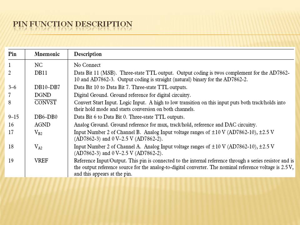
Pin |
Mnemonic |
Description |
|
1 |
NC |
No Connect |
|
2 |
DB11 |
Data Bit 11 (MSB). Tłiree-state TTL output. Output coding is twos complement for the AD7862-10 and AD7862-3. Output coding is straight (natural) binary for the AD7862-2. |
|
3-6 |
DB10-DB7 |
Data Bit 10 to Data Bit 7. Tłiree-state TTL outputs. |
|
7 |
DGND |
Digital Ground. Ground reference for digital circuitry. |
|
8 |
CONYST |
Convert Start Input. Logic Input. A high to Iow transition on this input puts both trackholds into their hołd modę and starts conversion on both channels. |
|
9-15 |
DB6-DB0 |
Data Bit 6 to Data Bit 0. Tłiree-state TTL outputs. |
|
16 |
AGND |
Analog Ground. Ground reference for mux, track/hold, reference and DAC circuitn*. |
|
17 |
VB2 |
Input Number 2 of Channel B. Analog Input voltage ranges of ± 10 V (AD7862-10), ±2.5 V (AD7862-3) and 0 Y-2.5 V (AD7862-2). |
|
18 |
Va2 |
Input Number 2 of Channel A. Analog Input voltage ranges of ± 10 V (AD7862-10), ±2.5 V (AD7862-3) and 0 Y-2.5 V (AD7862-2). |
|
19 |
VREF |
Reference Input/Output. This pin is connected to the internal reference tłirougłi a series resistor and is the output reference source for the analog-to-digital converter. Tlie nominał reference voltage is 2.5 V, and this appears at the pin. |
Wyszukiwarka
Podobne podstrony:
Slajd17 (161) AD5342 PIN FUNCTION DESCRIPTIONS Pin No. Mnemonic Function 1 GAIN Gain Control Pin.
48281 Slajd29 (127) PIN FUNCTION DESCRIPTION 20 A0 Multiplexer Select. This iuput is used in conju
IC AT500 c@@@o©@ ę©@©©©@
Slajd25 (147) AD7862 - FUNCTIONAŁ BŁOCK DIAGRAM VreF
Security Modę Modę Description Disabled No encryption set (not recommended!) WPA
70477 Slajd22 (135) Politechnika WrocławskaTOROWISKA TRAMWAJOWE Szerokość torowiska zależy od lokali
0bffa3cb534f1063 10. Znwmlolć piń< bnli.y w glebach INilsl:! wolut Kię w pr/.cd
18329 Slajd23 (135) Politechnika WrocławskaŁUKI KOŁOWE « wymagania Najmniejsze zalecane długości luk
s004 Short out pin-B 5 and •3 on the connector..1 1$-pin AL DL test pług
więcej podobnych podstron