Slajd17 (161)
AD5342 PIN FUNCTION DESCRIPTIONS
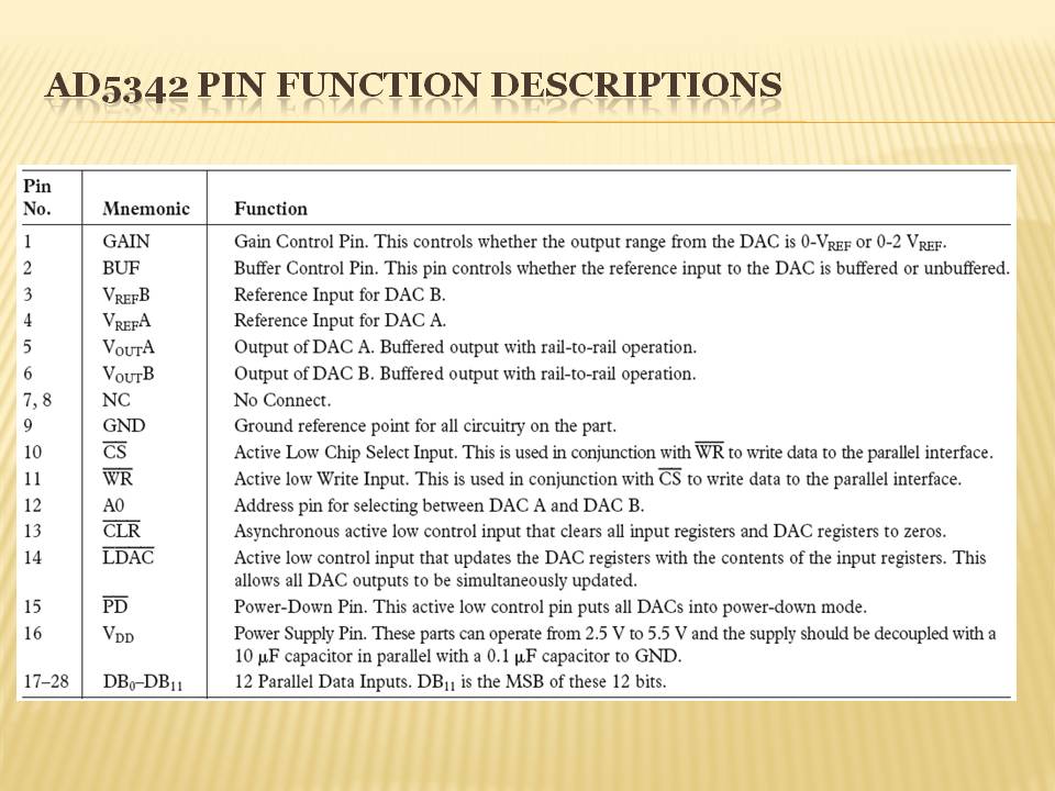
|
Pin No. |
Mnemonic |
Function |
|
1 |
GAIN |
Gain Control Pin. This Controls whether the output rangę from tłie DAG is 0-Vref ot 0-2 Vref. |
|
2 |
BUF |
Buffer Control Pin. This pin Controls whether the reference input to the DAC is buffered or unbuffered. |
|
3 |
VrefB |
Reference Input for DAC B. |
|
4 |
vrefA |
Reference Input for DAC A. |
|
5 |
VoutA |
Output of DAC A. Buffered output with rail-to-rail operation. |
|
6 |
VoutB |
Output of DAC B. Buffered output with rail-to-rail operation. |
|
7,8 |
NC |
No Connect. |
|
9 |
GND |
Ground reference point for all circuitry on the part. |
|
10 |
CŚ |
Active Low Chip Select Input. This is used in conjunction with WR to write data to the parallel interface. |
|
11 |
WR |
Active low Write Input. This is used in conjunction with CS to write data to the parallel interface. |
|
12 |
A0 |
Address pin for selecting between DAC A and DAC B. |
|
13 |
CLR |
Asynchronous active low control input that clears all input registers and DAC registers to zeros. |
|
14 |
LDAC |
Active low control input that updates the DAC registers with the contents of the input registers. This allows all DAC outputs to be simultaneously updated. |
|
15 |
PD |
Power-Down Pin. This active low control pin puts all DACs into power-down modę. |
|
16 |
Vdd |
Power Supply Pin. These parts can operate from 2.5 V to 5.5 V and the supply should be decoupled with a 10 jaF capacitor in parallel with a 0.1 \i¥ capacitor to GND. |
|
17-28 |
DBo-DBn |
12 Parallel Data Inputs. DBn is the MSB of these 12 bits. |
Wyszukiwarka
Podobne podstrony:
Slajd28 (135) PIN FUNCTION DESCRIPTION Pin Mnemonic Description 1 NC No Connect 2 DB11 Data Bit
63104 Slajd15 (172) AD5342GENERAL DESCRIPTION The AD5332/AD5333/AD5342/AD5343 are dual 8-, 10-, and
66065 Slajd15 (171) BQ4»02 - PARALLEL REAJL-TIME CLOCK TERMINAL 1/0 DESCRIPTION NAME NO. AO 10
Slajd18 (161) BQ48o2 - PARAJLLEL REAL-TIME CLOCK NOTES A WE isheld high for a read cycle. _ B Deyice
Slajd19 (160) AD5342 - TIMING CHARACTERISTICS Parameter Limit at Tmin, Tmax Unit Condition/Comment
Security Modę Modę Description Disabled No encryption set (not recommended!) WPA
Slajd16 (166) AI>5342 FUNCTIONAL BŁOCK DIAGRAM VREFa Vdd
Slajd18 (162) AD5342- PARALLELINTERFACETIMING DIAGRAM 2ASYNCHRONOUSlDaC update modę
więcej podobnych podstron