cdx 4250rv djvu
|
Model Name Using Similar Mechanism |
CDX-C570R/C580R |
|
CD Drive Mechanism Type |
MG-363T-121 |
|
Optical Pick-up Name |
KSS-521A |
|
CD player sectlon |
Power amplifier section | ||
|
System |
Compact disc digital audio |
Outputs |
Speaker outputs |
|
system |
(surę seal connectors) | ||
|
Signal-to-noise ratio |
90 dB |
Speaker impedance |
4-8 nłmis |
|
Freąuency response |
10 - 20,000 Hz |
Maximum power output 35 W x 4 (at 4 ohms) | |
|
Wow and flutter |
Below measurable limit | ||
|
General | |||
|
Tuner section |
Outputs |
Lineoutput(l) | |
|
FM |
Power aerial relay control | ||
|
Timing rangę |
87.5 -108.0 MHz |
lead | |
|
Aerial terminal |
Extemal aerial connector |
Power amplifier control | |
|
Intermediate freąuency |
10.7 MHz |
lead | |
|
Usable sensitivity |
12 dBf |
Telephone ATT control | |
|
Selectivity |
75 dBat 400 kHz |
lead | |
|
Signal-to-noise ratio |
65 dB (stereo), |
Tonę Controls |
Bass ±8 dB at 100 Hz |
|
68 dB (mono) |
Treble ±8 dB at 10 kHz | ||
|
Harmonie distordon at 1 |
kHz |
Power reąuirements |
12 V DC car battery |
|
0.8% (stereo), |
(negative ground) | ||
|
0.6% (mono) |
Dimensions |
Approx. 178 x 50 x 185 mm | |
|
Separation |
35 dB at 1 kHz |
(w/h/d) | |
|
Freąuency response |
30-15,000 Hz |
Mounting dimension |
Approx. 182 x 53 x 162 mm |
|
(w/h/d) | |||
|
MW/LW |
Mass |
Approx. 1.2 kg | |
|
Tuning rangę |
MW: 531 -1,602 kHz |
Supplied accessories |
Parts for installation and |
|
LW: 153-281 kHz |
connections (1 set) | ||
|
Aerial terminal |
Extemal aerial connector |
Front panel case (1) | |
|
Intermediate freąuency |
10.7 MHz/450 kHz | ||
|
Sensithrity |
MW: 30 iiV |
Design and specifications are subject to change without | |
|
LW:50^iV |
notice. | ||

MICROFILM
FMMWI1W COMPACT MSCPUNER
SONY.
®
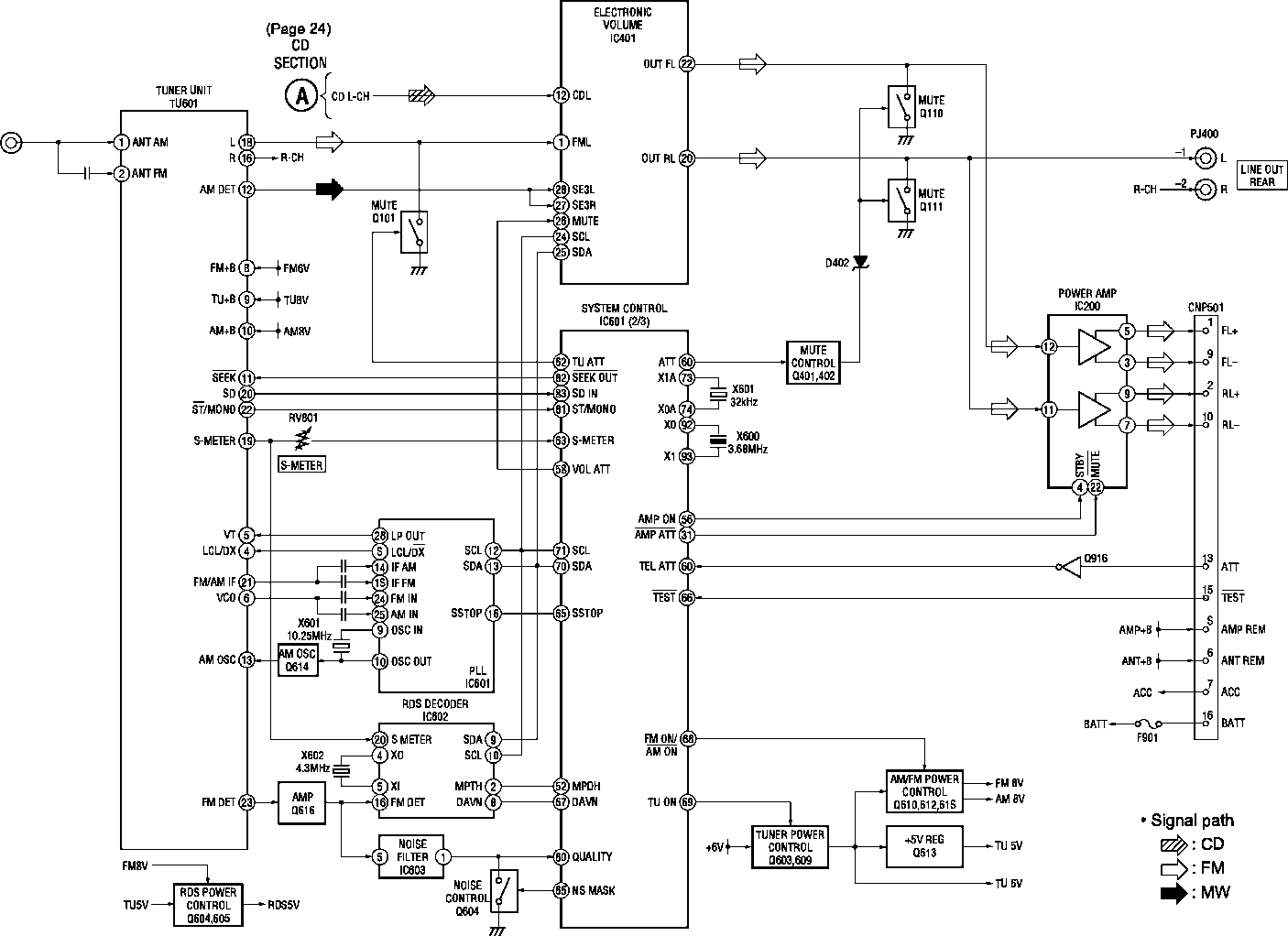
TUNER SECTION (Page 25)
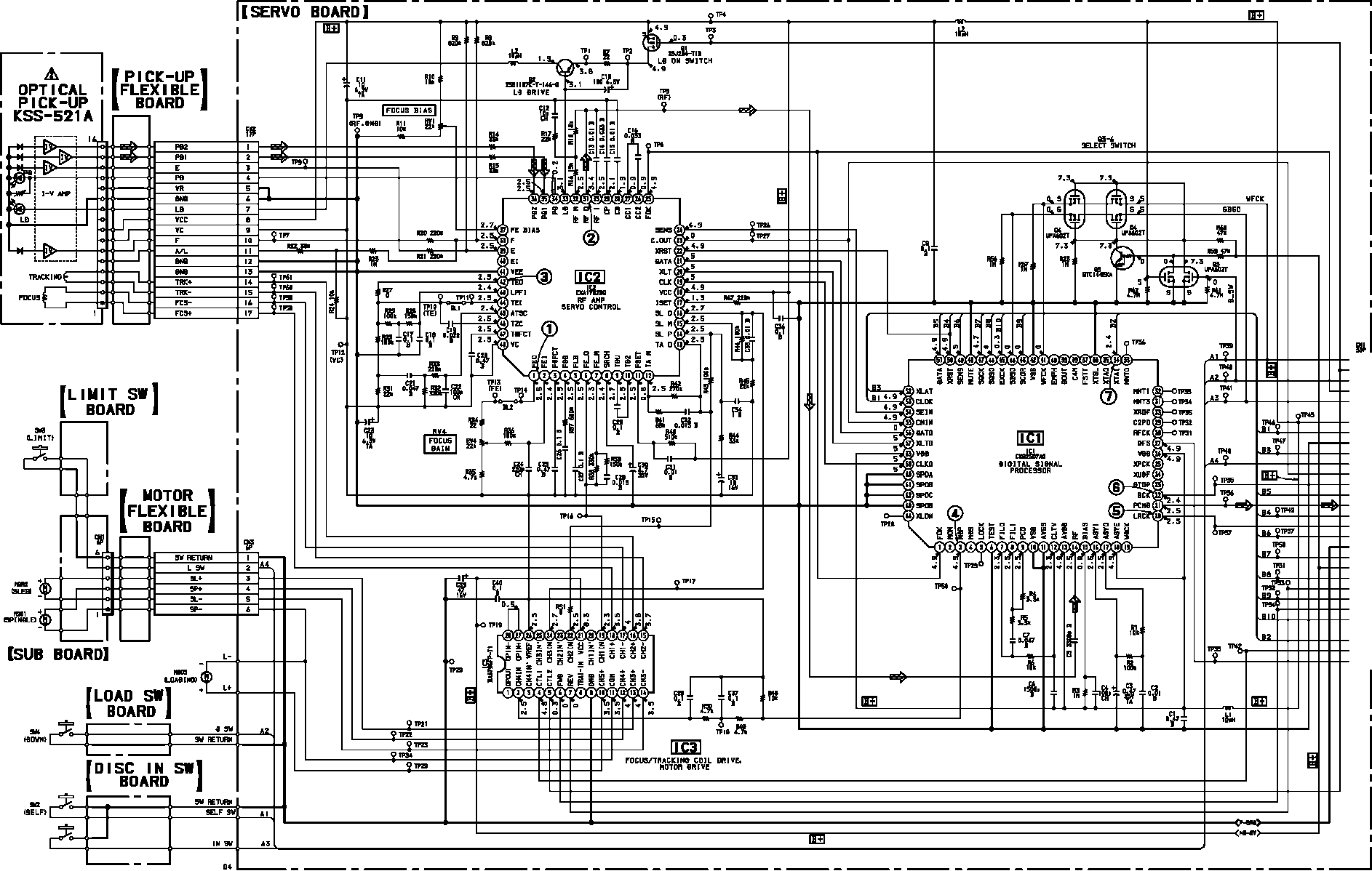
OPTICAL PICK-UP KSS-521A
RFAMP, SERV0 CONTROL IC2
DIGITAL SIGNAL PROESSOR IC1
D/A CONVERTER IC702
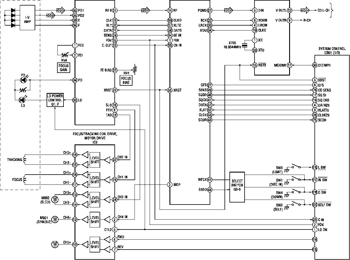
M903
(LOADING)
Signal path
^>: CD
04
CNJ600
(ANTENNA)
-25
26-
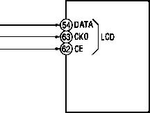
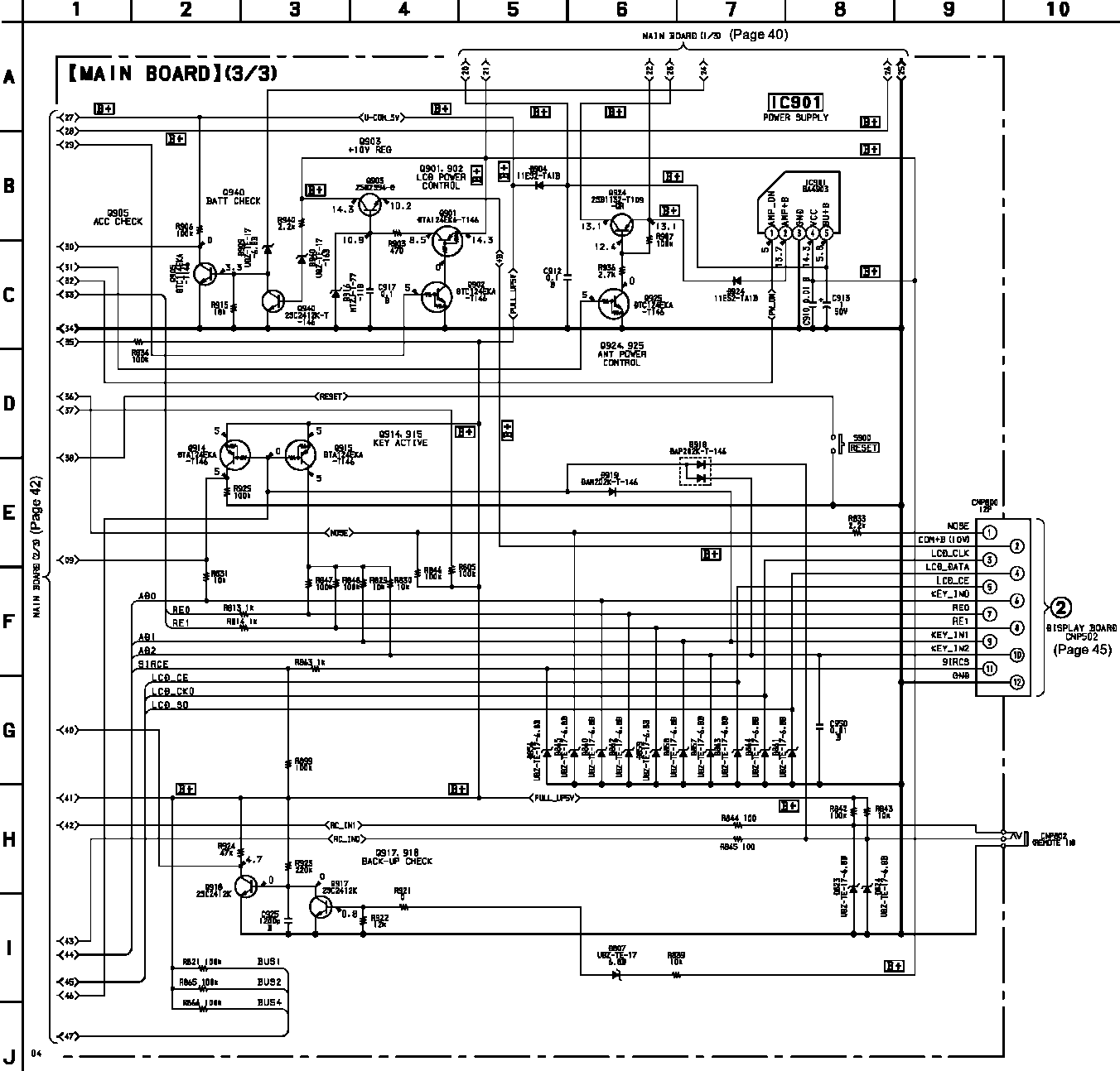
SYSTEM CONTROL IC601 (3/3)
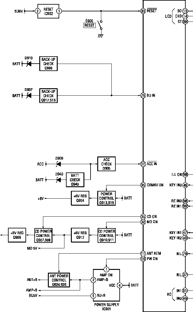
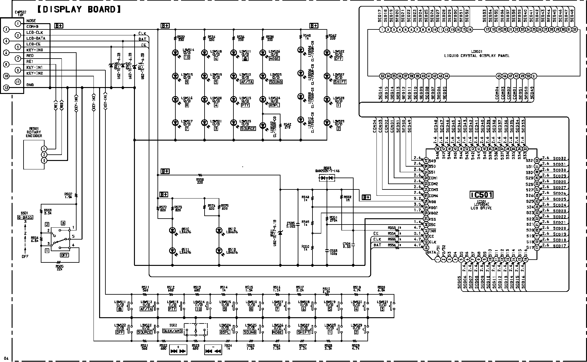
LCD DRIVE IC501
BAnf
LCD POWER CONTROL Q901,902
+10V REG Q903
LCDS01

LED502,604,606,S08,510 LSW511-529
D510,511
&
D512,513
+10V
KEY MATRIX LSWS11-S29 S502
KEY ACTIVE Q914,915
A
V.
D916
T\/ n CNP802 *-' N{REMOTEIN)
V-
4-5. CIRCUIT BOARDS LOCATION
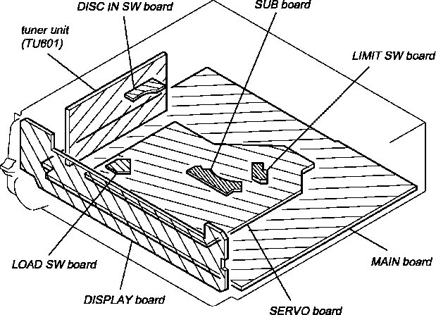
THIS NOTĘ IS COMMON FOR PRINTED WIRING BOARDS AND SCHEMATIC DIAGRAMS.
(In addition to thla, the necessary notę is prlnted In each błock.)
for schematic diagram:
• Ali capacitors are inp.Funlessotherwise noted. pF: jj+łF 50 WV or less are not indicated except for electrolytics and tantalums.
• Ali resistors are in O and 1A W or less unless otherwise specified.
• % : indicates tolerance.
• a : intemal component.
• i i : panel designation.
Notę: The components identified by mark A or dotted linę with mark A are critical for safety.
Replace only with part number specified.
• IB + I : B+ Linę.
• Power voltage isdc 14.4V and fed with regulated dc power supply from ACC and BATT cords.
• Voltages are taken with a VOM (Input impedance 10 MO). Voltage variations may be noted due to normal produc-tion tolerances.
• Waveforms are taken with a oscilloscope.
Voltage variations may be noted due to normal produc-tion tolerances.
• Circled numbers refer to waveforms.
• Signal path. c> : FM
: MW ^ : CD
• Abbreviation
G : German model.
for printed wiring boards:
• o : parts extracted from the component side.
• -: parts extracted from the conductor side.
• o ; Through hole.
• siiS: Pattem from the side which enables seeing.
(The other layer’s pattems are not indicated.)
Caution:
Pattem face side: Parts on the pattem face side seen from the (Side B) pattem face are indicated.
Parts face side: Parts on the parts face side seen from the (Side A) parts face are indicated.
• Abbreviation
G : German model.

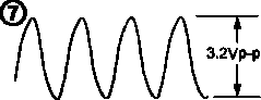
IC2 CD (FEO)
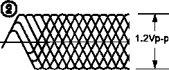

Approx. 2DDmVp-p
IC2 @ (TEO)
~~r
2.6Vp-p
7.6jisec
®
IJUliTr-
-|474nsec
6
8
9
11
12
J_13_L
14
J_15_L
16
9fl
(OISC IN)
|
1 |
SELF-SN/WFCK |
|
2 |
LfiON |
|
3 |
oc |
|
4 |
FOK |
|
5 |
IN_SW/SBS0 |
|
4 |
SERWO 5V |
|
7 |
SERWO SW |
|
B |
CL0K25 |
|
BNO | |
|
10 |
KLAT25 |
|
11 |
l_SV |
|
12 |
C.0UT |
|
13 |
bck eoun |
|
14 |
BATA25 |
|
15 |
PCNB |
|
14 |
XRST0 |
|
17 |
LRCK (HB2) |
|
18 |
SENS |
|
BNO <H0 | |
|
20 |
S0CK |
|
21 |
NB BW |
|
22 |
soso |
|
23 |
REW ILOAtt |
|
24 |
SCOB |
|
25 |
FWBEJECD |
|
24 |
EXCK |
|
27 |
CTL2 |
|
28 |
C14HIN |
|
29 |
CTLI |
|
30 |
OFS |
NAIN BOARS (Page 39)
XD
Notę:
• Voltage and wave1brms are dc with respect to ground under no-signal conditions. no mark : CD PLAY
* : Impossible to measure
-33
34-
4-9. SCHEMATIC DIAGRAM — MAIN SECTION (1/3) — • Refer to page 51 for IC Błock Diagrams. _]_I_?_|_3_|_4_|_5_|_6_|_7_|_8_L
J_lo_L
H
9
11
| 12 | 13 | 14 | 15 | 16 | 17 |
18
i
S°
S
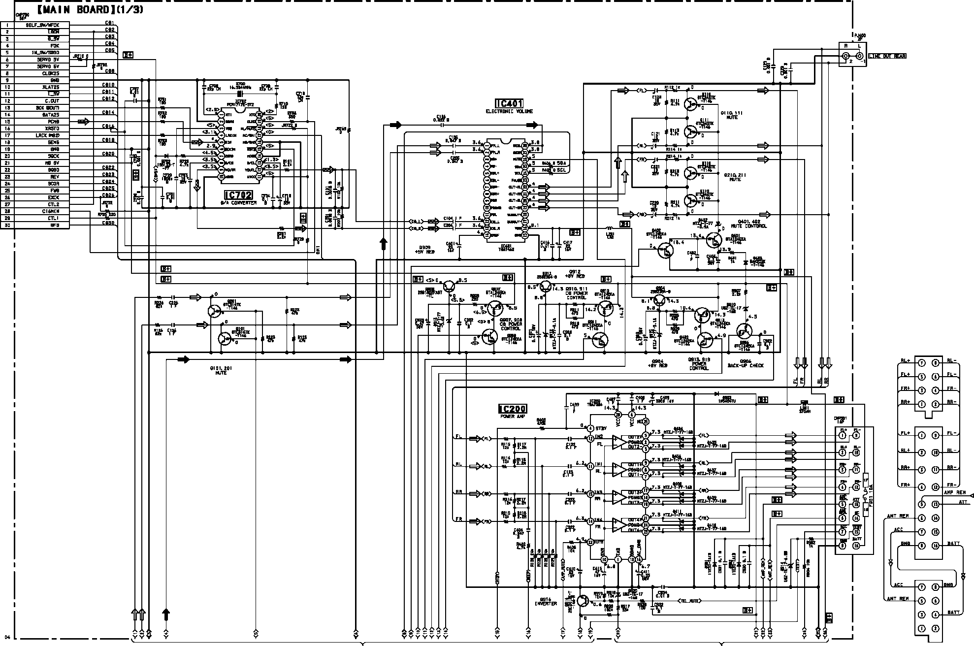
NAIN BOARB (2/9
(Page 42)
NAIN 90ARBB/9
(Page 43)
Notę:
• Voltage is dc with respect to ground under no-signal (detuned) condition. no mark : FM ( ) : MW
< > : CD PLAY
-39-
-40-
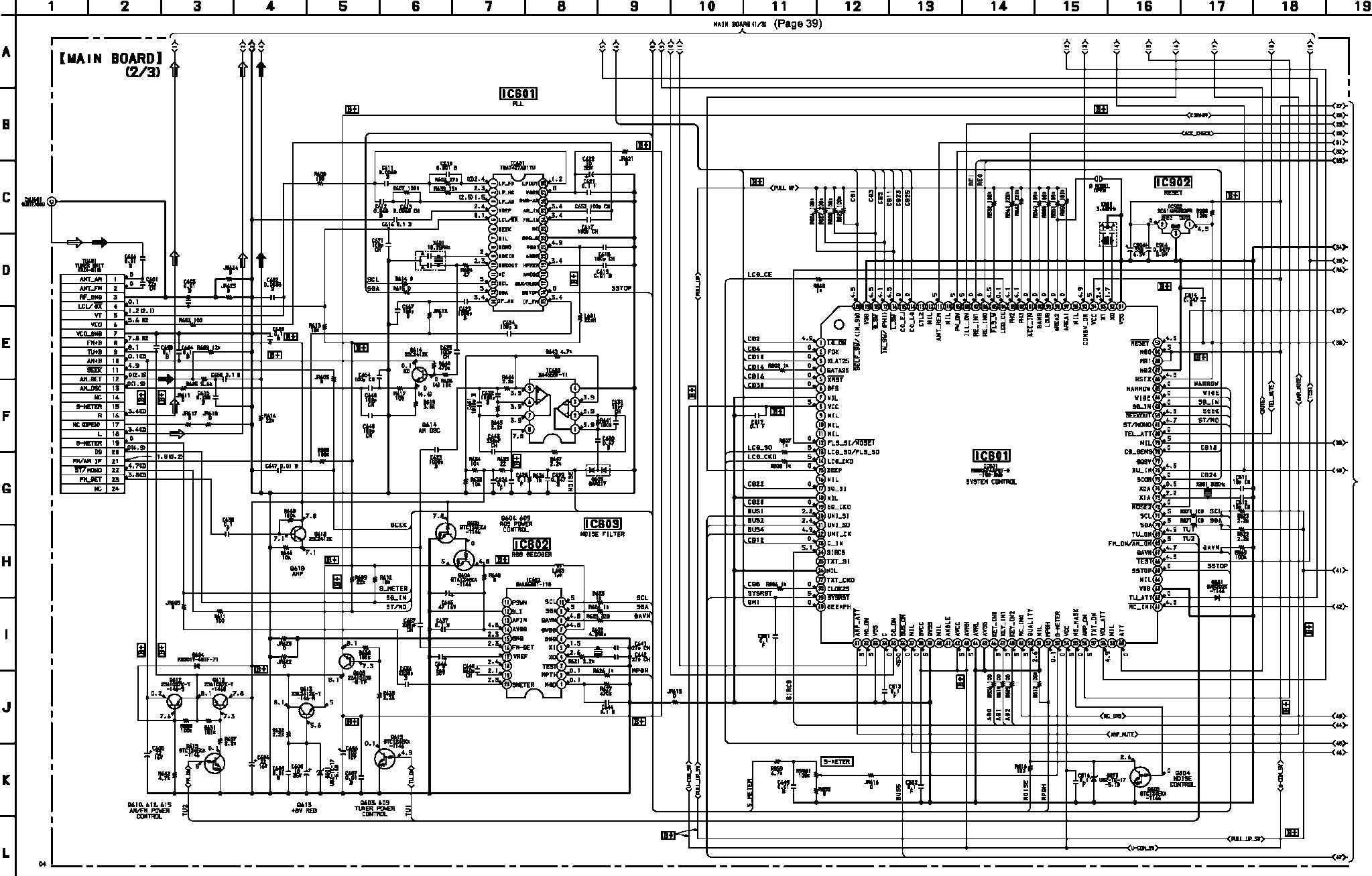
nain Bo*™ o/s (Page 43)
Notę:
• Voltage is dc with respect to ground under no-signal (detuned) condition. no mark : FM ( ): MW
< > : CD PLAY
Notę:
• Voltage is dc with respect to ground under no-signal (detuned) condition. no mark : FM ( ) : MW
< > : CD PLAY
8
10
11
12
13
B
H
MAlN BDARO (3/3 CNPGOO
(Page 44)
Notę:
• Voltage is dc with respect to ground under no-signal (detuned) condition. no mark : FM
-45 46-
Wyszukiwarka
Podobne podstrony:
cdx 3900 djvu CDX-3900R/4000R/4000RX AEP Model UK ModelSERVICE MANUAŁ Ver 1.2 2001.05 Model Name U
xr3550 1 tif ANTl Model Name Using Similar Machanism Tap* Transport Machanism Typa XR-3050/3062 MG-7
cdx 600 djvu CDX-600/606/626SERVICE MANUAŁUS Model CDX-600/606Canadian Model AEP Model UK Model
TV2050MK5 djvu CHASSIS SCHEMATIC DIAGRAM MODEL: TV2050MK5 ’ C3 JKK., 1 lE3The Shematic Diagram from
milliseconds and 1 microsecond (depending on frequency). Model 4110 is similar in all respects, exce
Pioneer KEH P4500R djvu PIONEER The Art of Entertainment ServiceManuał KEH-P4500R/X1M/EW ORDER NO. C
0 0173 LA 1311ATW02 Model Name : ATW02BŁOCK DIAGRAM "ramwrnr ■BismBnmnr
0 0173 LA 1311ATW02 Model Name : ATW02BŁOCK DIAGRAM "ramwrnr ■BismBnmnr
Model Standardowy - teoria pola Mechanika klasyczna - równania na wielkości takie jak pęd, energia p
0 0157 LA 1541BTS88 MODEL NAME :BTS88REV:0.3 Pentium4/Noi tliwood mPGA478 CPU CLOCK ICS950810 CRT &a
0 0163 LA 1432ATR60 MODEL NAME : ATR60 LA-1432REV:1.0 Northwood uF CBGA/uF CPGA CPU CRT & TY-OUT
0 0173 LA 1311ATW02 Model Name : ATW02BŁOCK DIAGRAM "ramwrnr ■BismBnmnr
Flashowanie ROM 1 plikowy M OdinB v3.04 X Odin3 Model Name :)mś PASS! 04:21 ID:COM Opti
Flashowanie ROM 3 plikowy Odin3 Model Name :) ID:COM 0:[COM7] Option
Audi bmp Audi model radia: RNS-E Aisin styk złącze główne złącze A (CD-C) złącze B 1 - MOST
więcej podobnych podstron