456719255

MICROPROCESSOR INTERFACE
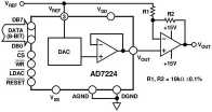
Mismatch between R1 and R2 causes gain and offset errors; therefore, these resistors must match and track over temperaturę. Once again, the AD7224 can be operated in single supply or ffom positive/negative supplies. Table III shows the digital codę versus output voltage relationship for the Circuit of Figurę 6 with R1 = R2.

Figurę 6. Bipolar Output Circuit
Table III. Bipolar (Offset Binary) Codę Table
DAC Register Contents MSB LSB

Figurę 8. AD7224 to 8085A/8088 Interface
Analog Output

Figurę 9. AD7224 to 6809/6502 Interface

1111 1111

Figurę 10. AD7224 to Z-80 Interface
AGND BIAS
The AD7224 AGND pin can be biased above system GND (AD7224 DGND) to provide an offset “zero” analog output voltage level. Figurę 7 shows a Circuit configuration to achieve this. The output voltage, V0UT, is expressed as:
V0ut =VBIA s + D-(Vm)
where D is a fractional representation of the digital word in DAC register and can vary ffom 0 to 255/256.
For a given increasing AGND above system GND will re-duce the effective Vdd~Vref which must be at least 4 V to en-sure specified operation. Notę that VDd and V$s for the AD7224 must be referenced to DGND.

Figurę 11. AD7224 to 68008 Interface
REV. B
-7-
Wyszukiwarka
Podobne podstrony:
vag interface R1-10k R2 - 2,2 k R3- 10 k RA- A, 5 k C2- 1uF/50V C3- 1uF/50 V&nbs
00090 ?d1d351fe584f51c4e23c939fd54473 89 A Very Simple Set of Process Control Rules ZONĘ SCORE b
00106 ?07bfb68ef5340d339a4e323754f6b8 106 McWilliams parameters such as the sample size, time betwe
4-18 4.8 Mounting and Dismounting the Module. CHAPTER 5 ASSIGNMENT I (MC PROTOCOL COMMUNICATION BETW
QUESTION NO: 10 When files are transferred between a host and an FTP server, the data is divided int
When comparing and contrasting the similarities and differences between bridges and switches, which
WIESŁAW SONCZYK ŁUKASZ SZURMIŃSKI KRZYSZTOF ŚWIREK RYSZARD TADEUSIEWICZ Research. Between West and
WIESŁAW SONCZYK ŁUKASZ SZURMIŃSKI KRZYSZTOF ŚWIREK RYSZARD TADEUSIEWICZ and Research. Between West a
więcej podobnych podstron