456719269
SELECTED PAGES ONLY!


FEATURES
8-Bit CMOS DAC with Output Amplifiers Operates with Single or Dual Supplies Low Total Unadjusted Error:
Less Than 1 LSB Over Temperaturę Extended Temperaturę Rangę Operation pP-Compatible with Double Buffered Inputs Standard 18-Pin DIPs, and 20-Terminal Surface Mount Package and SOIC Package
GENERAL DESCRIPTION
The AD7224 is a precision 8-bit voltage-output, digital-to-analog converter, with output amplifier and double buffered interface logie on a monolithic CMOS chip. No extemal trims are reąuired to achieve fuli specified performance for the part.
PRODUCT HIGHLIGHTS
1. DAC and Amplifier on CMOS Chip
The single-chip design of the 8-bit DAC and output amplifier is inherently morę reliable than multi-chip designs. CMOS fabrication means low power consumption (35 mW typical with single supply).
2. Low Total Unadjusted Error
The fabrication of the AD7224 on Analog Devices Linear Compatible CMOS (LC2MOS) process coupled with a novel DAC switch-pair arrangement, enables an excellent total unadjusted error of less than 1 LSB over the fuli operating temperaturę rangę.
3. Single or Dual Supply Operation
The voltage-mode configuration of the AD7224 allows operation from a single power supply raił. The part can also be op-erated with dual supplies giving enhanced performance for some parameters.
4. Versatile Interface Logic
The high speed logie allows direct interfacing to most microprocessors. Additionally, the double buffered interface enables simultaneous update of the AD7224 in multiple DAC systems. The part also features a zero override function.
REV. B
One Technology Way, P.O. Box 9106, Norwood. MA 02062-9106, U.S.A. Tel: 617/329-4700 Fax: 617/326-8703
Information furnished by Analog Devices is believed to be accurate and reliable. However, no responsibility Is assumed by Analog Deyices for its use, nor for any infringements of patents or other rights of third parties which may result from its use. No license is granted by implication or otherwise under any patent or patent rights of Analog Deyices.
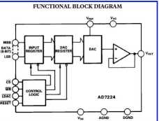
The double buffered interface logie consists of two 8-bit regis-ters-an input register and a DAC register. Only the data held in the DAC registers determines the analog output of the con-verter. The double buffering allows simultaneous update in a
system containing multiple AD7224S. Both registers may be_
madę transparent under control of three extemal lines, CS, \VR and LDAC. With both registers transparent, the RESET linę functions like a zero override; a useful funedon for system cali-brarion cycles. Ali logie inputs are TTL and CMOS (5 V) level compatible and the control logie is speed compatible with most 8-bit microprocessors.
Specified performance is guaranteed for input reference voltages from +2 V to +12.5 V when using dual supplies. The part is also specified for single supply operation using a reference of +10 V. The output amplifier is capable of developing +10 V across a
kfi load.
The AD7224 is fabricated in an all ion-implanted high speed Linear Compatible CMOS (LC2MOS) process which has been specifically developed to allow high speed digital logie circuits and precision analog circuits to be integrated on the same chip.
Wyszukiwarka
Podobne podstrony:
Compressed Table Characteristics Compressed storage format is a read-only format that is generated w
Measurements and Patterns pattern. For the patterns on the following pages, only half of the front&n
THE CUCKOO’S NEST Brand Style Guide
48281 Slajd29 (127) PIN FUNCTION DESCRIPTION 20 A0 Multiplexer Select. This iuput is used in conju
Select: f - quit, . - list users, 0x<RID> - User with
gallery settings type Gallery Settings Select the type of gallery you want to display. Set a feature
Preview Output Style Select a style and type of citation to preview. Output Style Sagę Vancouver * U
f4 12 Pioperty Page Wizard - Select the Pioperty Pages Choose the Property Page(s) you want to use w
Slajd14 (170) WYJŚCIA ANALOGOWE - AD5342 AD5343: Dual 12-Bit DAC iii 20-Lead TSSOP Low Power Operati
f9 5 lnbox Setup Wizard Select the information services(s] that you want to use with Microsoft Excha
Feature Reference 3 0 Open Task Select a task to open (? = any character, * = any String): ^ Open Ta
image001 analog * « The trouble with a humtn-model Computer it thatthe program it jo comph
image002 With u magtaine like Analog, you would. of ćoursc. e.tpect us to uxe computrn lor
więcej podobnych podstron