8155BS–AVR–07/09
Features
•
High-performance, Low-power AVR
®
8-bit Microcontroller
•
Advanced RISC Architecture
– 131 Powerful Instructions – Most Single-clock Cycle Execution
– 32 x 8 General Purpose Working Registers
– Fully Static Operation
– Up to 16 MIPS Throughput at 16 MHz
– On-chip 2-cycle Multiplier
•
High Endurance Non-volatile Memory segments
– 32K Bytes of In-System Self-programmable Flash program memory
– 1024 Bytes EEPROM
– 2K Byte Internal SRAM
– Write/Erase Cycles: 10,000 Flash/100,000 EEPROM
– Data retention: 20 years at 85°C/100 years at 25°C
– Optional Boot Code Section with Independent Lock Bits
• In-System Programming by On-chip Boot Program
• True Read-While-Write Operation
– Programming Lock for Software Security
•
JTAG (IEEE std. 1149.1 Compliant) Interface
– Boundary-scan Capabilities According to the JTAG Standard
– Extensive On-chip Debug Support
– Programming of Flash, EEPROM, Fuses, and Lock Bits through the JTAG Interface
•
Peripheral Features
– Two 8-bit Timer/Counters with Separate Prescalers and Compare Modes
– One 16-bit Timer/Counter with Separate Prescaler, Compare Mode, and Capture
Mode
– Real Time Counter with Separate Oscillator
– Four PWM Channels
– 8-channel, 10-bit ADC
• 8 Single-ended Channels
• 7 Differential Channels in TQFP Package Only
• 2 Differential Channels with Programmable Gain at 1x, 10x, or 200x
– Byte-oriented Two-wire Serial Interface
– Programmable Serial USART
– Master/Slave SPI Serial Interface
– Programmable Watchdog Timer with Separate On-chip Oscillator
– On-chip Analog Comparator
•
Special Microcontroller Features
– Power-on Reset and Programmable Brown-out Detection
– Internal Calibrated RC Oscillator
– External and Internal Interrupt Sources
– Six Sleep Modes: Idle, ADC Noise Reduction, Power-save, Power-down, Standby
and Extended Standby
•
I/O and Packages
– 32 Programmable I/O Lines
– 40-pin PDIP, 44-lead TQFP, and 44-pad QFN/MLF
•
Operating Voltages
– 2.7 - 5.5V for ATmega32A
•
Speed Grades
– 0 - 16 MHz for ATmega32A
•
Power Consumption at 1 MHz, 3V, 25
°C for ATmega32A
– Active: 0.6 mA
– Idle Mode: 0.2 mA
– Power-down Mode: < 1 µA
8-bit
Microcontroller
with 32K Bytes
In-System
Programmable
Flash
ATmega32A
Summary
2
8155BS–AVR–07/09
ATmega32A
1.
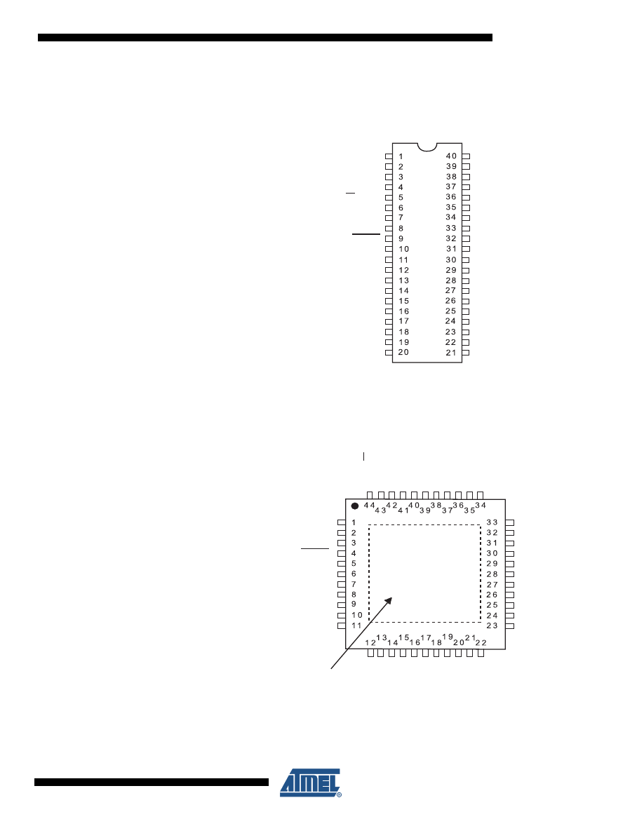
Pin Configurations
Figure 1-1.
Pinout ATmega32A
(XCK/T0) PB0
(T1) PB1
(INT2/AIN0) PB2
(OC0/AIN1) PB3
(SS) PB4
(MOSI) PB5
(MISO) PB6
(SCK) PB7
RESET
VCC
GND
XTAL2
XTAL1
(RXD) PD0
(TXD) PD1
(INT0) PD2
(INT1) PD3
(OC1B) PD4
(OC1A) PD5
(ICP1) PD6
PA0 (ADC0)
PA1 (ADC1)
PA2 (ADC2)
PA3 (ADC3)
PA4 (ADC4)
PA5 (ADC5)
PA6 (ADC6)
PA7 (ADC7)
AREF
GND
AVCC
PC7 (TOSC2)
PC6 (TOSC1)
PC5 (TDI)
PC4 (TDO)
PC3 (TMS)
PC2 (TCK)
PC1 (SDA)
PC0 (SCL)
PD7 (OC2)
PA4 (ADC4)
PA5 (ADC5)
PA6 (ADC6)
PA7 (ADC7)
AREF
GND
AVCC
PC7 (TOSC2)
PC6 (TOSC1)
PC5 (TDI)
PC4 (TDO)
(MOSI) PB5
(MISO) PB6
(SCK) PB7
RESET
VCC
GND
XTAL2
XTAL1
(RXD) PD0
(TXD) PD1
(INT0) PD2
(INT1) PD3
(OC1B) PD4
(OC1A) PD5
(ICP1) PD6
(OC2) PD7
VCC
GND
(SCL) PC0
(SDA) PC1
(TCK) PC2
(TMS) PC3
PB4 (SS)
PB3 (AIN1/OC0)
PB2 (AIN0/INT2)
PB1 (T1)
PB0 (XCK/T0)
GND
VCC
PA0 (ADC0)
PA1 (ADC1)
PA2 (ADC2)
PA3 (ADC3)
PDIP
TQFP/MLF
Note:
Bottom pad should
be soldered to ground.
3
8155BS–AVR–07/09
ATmega32A
2.
Overview
The ATmega32A is a low-power CMOS 8-bit microcontroller based on the AVR enhanced RISC
architecture. By executing powerful instructions in a single clock cycle, the ATmega32A
achieves throughputs approaching 1 MIPS per MHz allowing the system designer to optimize
power consumption versus processing speed.
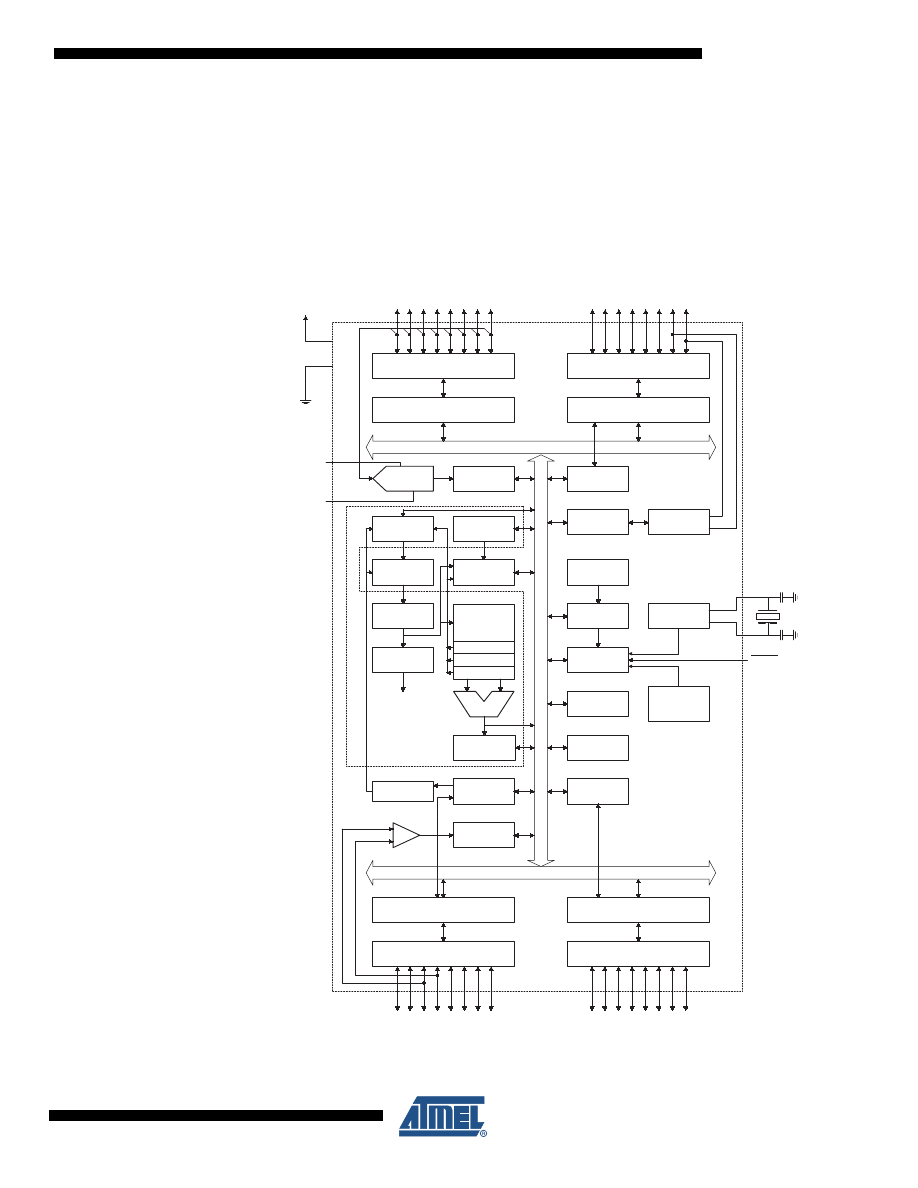
2.1
Block Diagram
Figure 2-1.
Block Diagram
INTERNAL
OSCILLATOR
OSCILLATOR
WATCHDOG
TIMER
MCU CTRL.
& TIMING
OSCILLATOR
TIMERS/
COUNTERS
INTERRUPT
UNIT
STACK
POINTER
EEPROM
SRAM
STATUS
REGISTER
USART
PROGRAM
COUNTER
PROGRAM
FLASH
INSTRUCTION
REGISTER
INSTRUCTION
DECODER
PROGRAMMING
LOGIC
SPI
ADC
INTERFACE
COMP.
INTERFACE
PORTA DRIVERS/BUFFERS
PORTA DIGITAL INTERFACE
GENERAL
PURPOSE
REGISTERS
X
Y
Z
ALU
+
-
PORTC DRIVERS/BUFFERS
PORTC DIGITAL INTERFACE
PORTB DIGITAL INTERFACE
PORTB DRIVERS/BUFFERS
PORTD DIGITAL INTERFACE
PORTD DRIVERS/BUFFERS
XTAL1
XTAL2
RESET
CONTROL
LINES
VCC
GND
MUX &
ADC
AREF
PA0 - PA7
PC0 - PC7
PD0 - PD7
PB0 - PB7
AVR CPU
TWI
AVCC
INTERNAL
CALIBRATED
OSCILLATOR

4
8155BS–AVR–07/09
ATmega32A
The AVR core combines a rich instruction set with 32 general purpose working registers. All the
32 registers are directly connected to the Arithmetic Logic Unit (ALU), allowing two independent
registers to be accessed in one single instruction executed in one clock cycle. The resulting
architecture is more code efficient while achieving throughputs up to ten times faster than con-
ventional CISC microcontrollers.
The ATmega32A provides the following features: 32K bytes of In-System Programmable Flash
Program memory with Read-While-Write capabilities, 1024 bytes EEPROM, 2K byte SRAM, 32
general purpose I/O lines, 32 general purpose working registers, a JTAG interface for Boundary-
scan, On-chip Debugging support and programming, three flexible Timer/Counters with com-
pare modes, Internal and External Interrupts, a serial programmable USART, a byte oriented
Two-wire Serial Interface, an 8-channel, 10-bit ADC with optional differential input stage with
programmable gain (TQFP package only), a programmable Watchdog Timer with Internal Oscil-
lator, an SPI serial port, and six software selectable power saving modes. The Idle mode stops
the CPU while allowing the USART, Two-wire interface, A/D Converter, SRAM, Timer/Counters,
SPI port, and interrupt system to continue functioning. The Power-down mode saves the register
contents but freezes the Oscillator, disabling all other chip functions until the next External Inter-
rupt or Hardware Reset. In Power-save mode, the Asynchronous Timer continues to run,
allowing the user to maintain a timer base while the rest of the device is sleeping. The ADC
Noise Reduction mode stops the CPU and all I/O modules except Asynchronous Timer and
ADC, to minimize switching noise during ADC conversions. In Standby mode, the crystal/reso-
nator Oscillator is running while the rest of the device is sleeping. This allows very fast start-up
combined with low-power consumption. In Extended Standby mode, both the main Oscillator
and the Asynchronous Timer continue to run.
The device is manufactured using Atmel’s high density nonvolatile memory technology. The On-
chip ISP Flash allows the program memory to be reprogrammed in-system through an SPI serial
interface, by a conventional nonvolatile memory programmer, or by an On-chip Boot program
running on the AVR core. The boot program can use any interface to download the application
program in the Application Flash memory. Software in the Boot Flash section will continue to run
while the Application Flash section is updated, providing true Read-While-Write operation. By
combining an 8-bit RISC CPU with In-System Self-Programmable Flash on a monolithic chip,
the Atmel ATmega32A is a powerful microcontroller that provides a highly-flexible and cost-
effective solution to many embedded control applications.
The ATmega32A AVR is supported with a full suite of program and system development tools
including: C compilers, macro assemblers, program debugger/simulators, in-circuit emulators,
and evaluation kits.
2.2
Pin Descriptions
2.2.1
VCC
Digital supply voltage.
2.2.2
GND
Ground.
2.2.3
Port A (PA7:PA0)
Port A serves as the analog inputs to the A/D Converter.
Port A also serves as an 8-bit bi-directional I/O port, if the A/D Converter is not used. Port pins
can provide internal pull-up resistors (selected for each bit). The Port A output buffers have sym-

5
8155BS–AVR–07/09
ATmega32A
metrical drive characteristics with both high sink and source capability. When pins PA0 to PA7
are used as inputs and are externally pulled low, they will source current if the internal pull-up
resistors are activated. The Port A pins are tri-stated when a reset condition becomes active,
even if the clock is not running.
2.2.4
Port B (PB7:PB0)
Port B is an 8-bit bi-directional I/O port with internal pull-up resistors (selected for each bit). The
Port B output buffers have symmetrical drive characteristics with both high sink and source
capability. As inputs, Port B pins that are externally pulled low will source current if the pull-up
resistors are activated. The Port B pins are tri-stated when a reset condition becomes active,
even if the clock is not running.
Port B also serves the functions of various special features of the ATmega32A as listed on
page
59
.
2.2.5
Port C (PC7:PC0)
Port C is an 8-bit bi-directional I/O port with internal pull-up resistors (selected for each bit). The
Port C output buffers have symmetrical drive characteristics with both high sink and source
capability. As inputs, Port C pins that are externally pulled low will source current if the pull-up
resistors are activated. The Port C pins are tri-stated when a reset condition becomes active,
even if the clock is not running. If the JTAG interface is enabled, the pull-up resistors on pins
PC5(TDI), PC3(TMS) and PC2(TCK) will be activated even if a reset occurs.
The TD0 pin is tri-stated unless TAP states that shift out data are entered.
Port C also serves the functions of the JTAG interface and other special features of the
ATmega32A as listed on
page 62
.
2.2.6
Port D (PD7:PD0)
Port D is an 8-bit bi-directional I/O port with internal pull-up resistors (selected for each bit). The
Port D output buffers have symmetrical drive characteristics with both high sink and source
capability. As inputs, Port D pins that are externally pulled low will source current if the pull-up
resistors are activated. The Port D pins are tri-stated when a reset condition becomes active,
even if the clock is not running.
Port D also serves the functions of various special features of the ATmega32A as listed on
page
64
.
2.2.7
RESET
Reset Input. A low level on this pin for longer than the minimum pulse length will generate a
reset, even if the clock is not running. The minimum pulse length is given in
Table 27-1 on page
299
. Shorter pulses are not guaranteed to generate a reset.
2.2.8
XTAL1
Input to the inverting Oscillator amplifier and input to the internal clock operating circuit.
2.2.9
XTAL2
Output from the inverting Oscillator amplifier.

6
8155BS–AVR–07/09
ATmega32A
2.2.10
AVCC
AVCC is the supply voltage pin for Port A and the A/D Converter. It should be externally con-
nected to V
CC
, even if the ADC is not used. If the ADC is used, it should be connected to V
CC
through a low-pass filter.
2.2.11
AREF
AREF is the analog reference pin for the A/D Converter.
3.
Resources
A comprehensive set of development tools, application notes and datasheets are available for
download on http://www.atmel.com/avr.
Note:
1.
4.
Data Retention
Reliability Qualification results show that the projected data retention failure rate is much less
than 1 PPM over 20 years at 85°C or 100 years at 25°C.
7
8155BS–AVR–07/09
ATmega32A
5.
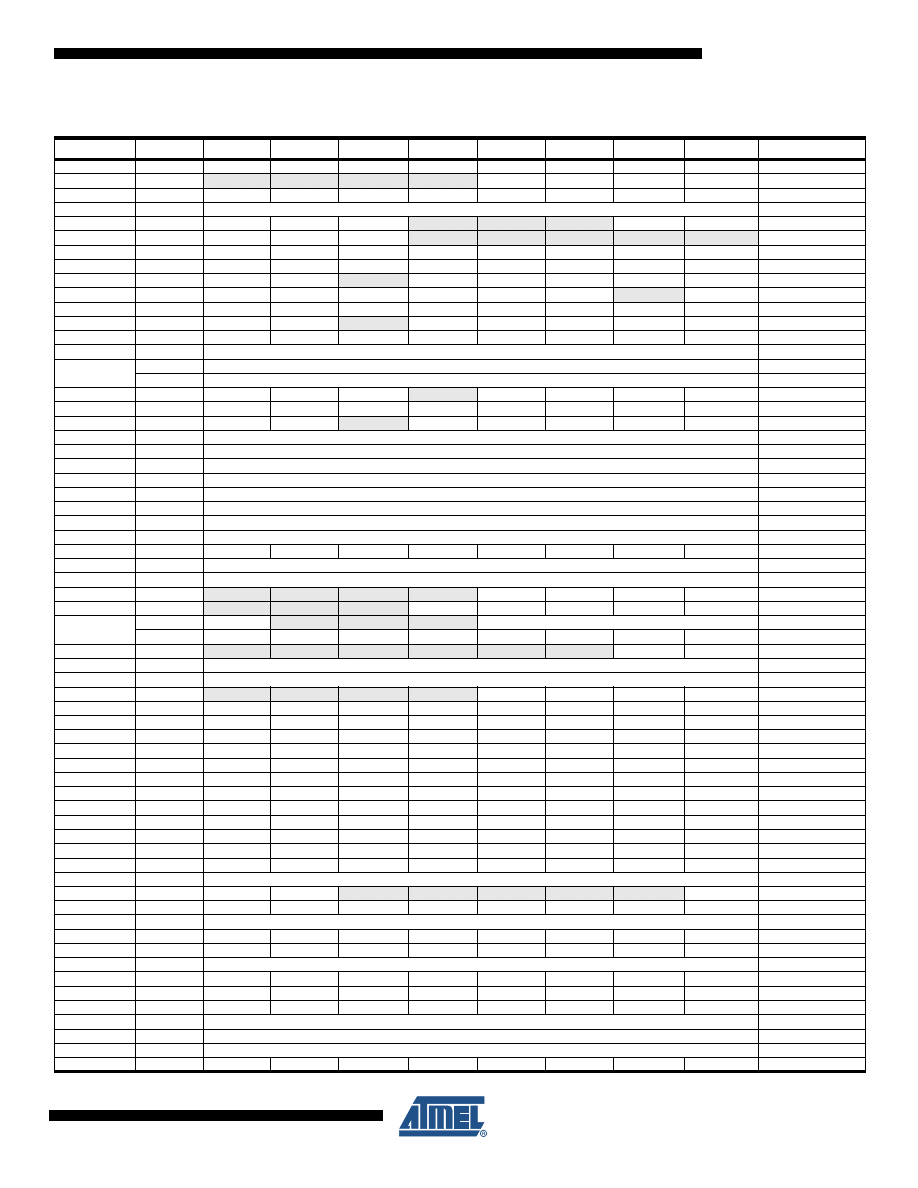
Register Summary
Address
Name
Bit 7
Bit 6
Bit 5
Bit 4
Bit 3
Bit 2
Bit 1
Bit 0
Page
$3F ($5F)
SREG
I
T
H
S
V
N
Z
C
8
$3E ($5E)
SPH
–
–
–
–
SP11
SP10
SP9
SP8
11
$3D ($5D)
SPL
SP7
SP6
SP5
SP4
SP3
SP2
SP1
SP0
11
$3C ($5C)
OCR0
Timer/Counter0 Output Compare Register
86
$3B ($5B)
GICR
INT1
INT0
INT2
–
–
–
IVSEL
IVCE
48, 71
$3A ($5A)
GIFR
INTF1
INTF0
INTF2
–
–
–
–
–
71
$39 ($59)
TIMSK
OCIE2
TOIE2
TICIE1
OCIE1A
OCIE1B
TOIE1
OCIE0
TOIE0
87, 117, 136
$38 ($58)
TIFR
OCF2
TOV2
ICF1
OCF1A
OCF1B
TOV1
OCF0
TOV0
87, 117, 136
$37 ($57)
SPMCR
SPMIE
RWWSB
–
RWWSRE
BLBSET
PGWRT
PGERS
SPMEN
264
$36 ($56)
TWCR
TWINT
TWEA
TWSTA
TWSTO
TWWC
TWEN
–
TWIE
202
$35 ($55)
MCUCR
SE
SM2
SM1
SM0
ISC11
ISC10
ISC01
ISC00
36, 69
$34 ($54)
MCUCSR
JTD
ISC2
–
JTRF
WDRF
BORF
EXTRF
PORF
42, 70, 251
$33 ($53)
TCCR0
FOC0
WGM00
COM01
COM00
WGM01
CS02
CS01
CS00
84
$32 ($52)
TCNT0
Timer/Counter0 (8 Bits)
86
$31
($51)
OSCCAL
Oscillator Calibration Register
32
OCDR
On-Chip Debug Register
232
$30 ($50)
SFIOR
ADTS2
ADTS1
ADTS0
–
ACME
PUD
PSR2
PSR10
66,90,137,206,226
$2F ($4F)
TCCR1A
COM1A1
COM1A0
COM1B1
COM1B0
FOC1A
FOC1B
WGM11
WGM10
112
$2E ($4E)
TCCR1B
ICNC1
ICES1
–
WGM13
WGM12
CS12
CS11
CS10
114
$2D ($4D)
TCNT1H
Timer/Counter1 – Counter Register High Byte
116
$2C ($4C)
TCNT1L
Timer/Counter1 – Counter Register Low Byte
116
$2B ($4B)
OCR1AH
Timer/Counter1 – Output Compare Register A High Byte
116
$2A ($4A)
OCR1AL
Timer/Counter1 – Output Compare Register A Low Byte
116
$29 ($49)
OCR1BH
Timer/Counter1 – Output Compare Register B High Byte
116
$28 ($48)
OCR1BL
Timer/Counter1 – Output Compare Register B Low Byte
116
$27 ($47)
ICR1H
Timer/Counter1 – Input Capture Register High Byte
116
$26 ($46)
ICR1L
Timer/Counter1 – Input Capture Register Low Byte
116
$25 ($45)
TCCR2
FOC2
WGM20
COM21
COM20
WGM21
CS22
CS21
CS20
132
$24 ($44)
TCNT2
Timer/Counter2 (8 Bits)
135
$23 ($43)
OCR2
Timer/Counter2 Output Compare Register
135
$22 ($42)
ASSR
–
–
–
–
AS2
TCN2UB
OCR2UB
TCR2UB
135
$21 ($41)
WDTCR
–
–
–
WDTOE
WDE
WDP2
WDP1
WDP0
43
$20
($40)
UBRRH
URSEL
–
–
–
UBRR[11:8]
171
UCSRC
URSEL
UMSEL
UPM1
UPM0
USBS
UCSZ1
UCSZ0
UCPOL
170
$1F ($3F)
EEARH
–
–
–
–
–
–
EEAR9
EEAR8
20
$1E ($3E)
EEARL
EEPROM Address Register Low Byte
20
$1D ($3D)
EEDR
EEPROM Data Register
21
$1C ($3C)
EECR
–
–
–
–
EERIE
EEMWE
EEWE
EERE
21
$1B ($3B)
PORTA
PORTA7
PORTA6
PORTA5
PORTA4
PORTA3
PORTA2
PORTA1
PORTA0
66
$1A ($3A)
DDRA
DDA7
DDA6
DDA5
DDA4
DDA3
DDA2
DDA1
DDA0
66
$19 ($39)
PINA
PINA7
PINA6
PINA5
PINA4
PINA3
PINA2
PINA1
PINA0
66
$18 ($38)
PORTB
PORTB7
PORTB6
PORTB5
PORTB4
PORTB3
PORTB2
PORTB1
PORTB0
67
$17 ($37)
DDRB
DDB7
DDB6
DDB5
DDB4
DDB3
DDB2
DDB1
DDB0
67
$16 ($36)
PINB
PINB7
PINB6
PINB5
PINB4
PINB3
PINB2
PINB1
PINB0
67
$15 ($35)
PORTC
PORTC7
PORTC6
PORTC5
PORTC4
PORTC3
PORTC2
PORTC1
PORTC0
67
$14 ($34)
DDRC
DDC7
DDC6
DDC5
DDC4
DDC3
DDC2
DDC1
DDC0
67
$13 ($33)
PINC
PINC7
PINC6
PINC5
PINC4
PINC3
PINC2
PINC1
PINC0
67
$12 ($32)
PORTD
PORTD7
PORTD6
PORTD5
PORTD4
PORTD3
PORTD2
PORTD1
PORTD0
67
$11 ($31)
DDRD
DDD7
DDD6
DDD5
DDD4
DDD3
DDD2
DDD1
DDD0
67
$10 ($30)
PIND
PIND7
PIND6
PIND5
PIND4
PIND3
PIND2
PIND1
PIND0
68
$0F ($2F)
SPDR
SPI Data Register
145
$0E ($2E)
SPSR
SPIF
WCOL
–
–
–
–
–
SPI2X
145
$0D ($2D)
SPCR
SPIE
SPE
DORD
MSTR
CPOL
CPHA
SPR1
SPR0
143
$0C ($2C)
UDR
USART I/O Data Register
167
$0B ($2B)
UCSRA
RXC
TXC
UDRE
FE
DOR
PE
U2X
MPCM
168
$0A ($2A)
UCSRB
RXCIE
TXCIE
UDRIE
RXEN
TXEN
UCSZ2
RXB8
TXB8
169
$09 ($29)
UBRRL
USART Baud Rate Register Low Byte
171
$08 ($28)
ACSR
ACD
ACBG
ACO
ACI
ACIE
ACIC
ACIS1
ACIS0
206
$07 ($27)
ADMUX
REFS1
REFS0
ADLAR
MUX4
MUX3
MUX2
MUX1
MUX0
222
$06 ($26)
ADCSRA
ADEN
ADSC
ADATE
ADIF
ADIE
ADPS2
ADPS1
ADPS0
224
$05 ($25)
ADCH
ADC Data Register High Byte
225
$04 ($24)
ADCL
ADC Data Register Low Byte
225
$03 ($23)
TWDR
Two-wire Serial Interface Data Register
203
$02 ($22)
TWAR
TWA6
TWA5
TWA4
TWA3
TWA2
TWA1
TWA0
TWGCE
204

8
8155BS–AVR–07/09
ATmega32A
Notes:
1. When the OCDEN Fuse is unprogrammed, the OSCCAL Register is always accessed on this address. Refer to the debug-
ger specific documentation for details on how to use the OCDR Register.
2. Refer to the USART description for details on how to access UBRRH and UCSRC.
3. For compatibility with future devices, reserved bits should be written to zero if accessed. Reserved I/O memory addresses
should never be written.
4. Some of the Status Flags are cleared by writing a logical one to them. Note that the CBI and SBI instructions will operate on
all bits in the I/O Register, writing a one back into any flag read as set, thus clearing the flag. The CBI and SBI instructions
work with registers $00 to $1F only.
$01 ($21)
TWSR
TWS7
TWS6
TWS5
TWS4
TWS3
–
TWPS1
TWPS0
203
$00 ($20)
TWBR
Two-wire Serial Interface Bit Rate Register
201
Address
Name
Bit 7
Bit 6
Bit 5
Bit 4
Bit 3
Bit 2
Bit 1
Bit 0
Page
9
8155BS–AVR–07/09
ATmega32A
6.
Instruction Set Summary
Mnemonics
Operands
Description
Operation
Flags
#Clocks
ARITHMETIC AND LOGIC INSTRUCTIONS
ADD
Rd, Rr
Add two Registers
Rd
← Rd + Rr
Z,C,N,V,H
1
ADC
Rd, Rr
Add with Carry two Registers
Rd
← Rd + Rr + C
Z,C,N,V,H
1
ADIW
Rdl,K
Add Immediate to Word
Rdh:Rdl
← Rdh:Rdl + K
Z,C,N,V,S
2
SUB
Rd, Rr
Subtract two Registers
Rd
← Rd - Rr
Z,C,N,V,H
1
SUBI
Rd, K
Subtract Constant from Register
Rd
← Rd - K
Z,C,N,V,H
1
SBC
Rd, Rr
Subtract with Carry two Registers
Rd
← Rd - Rr - C
Z,C,N,V,H
1
SBCI
Rd, K
Subtract with Carry Constant from Reg.
Rd
← Rd - K - C
Z,C,N,V,H
1
SBIW
Rdl,K
Subtract Immediate from Word
Rdh:Rdl
← Rdh:Rdl - K
Z,C,N,V,S
2
AND
Rd, Rr
Logical AND Registers
Rd
← Rd • Rr
Z,N,V
1
ANDI
Rd, K
Logical AND Register and Constant
Rd
← Rd • K
Z,N,V
1
OR
Rd, Rr
Logical OR Registers
Rd
← Rd v Rr
Z,N,V
1
ORI
Rd, K
Logical OR Register and Constant
Rd
← Rd v K
Z,N,V
1
EOR
Rd, Rr
Exclusive OR Registers
Rd
← Rd ⊕ Rr
Z,N,V
1
COM
Rd
One’s Complement
Rd
← $FF − Rd
Z,C,N,V
1
NEG
Rd
Two’s Complement
Rd
← $00 − Rd
Z,C,N,V,H
1
SBR
Rd,K
Set Bit(s) in Register
Rd
← Rd v K
Z,N,V
1
CBR
Rd,K
Clear Bit(s) in Register
Rd
← Rd • ($FF - K)
Z,N,V
1
INC
Rd
Increment
Rd
← Rd + 1
Z,N,V
1
DEC
Rd
Decrement
Rd
← Rd − 1
Z,N,V
1
TST
Rd
Test for Zero or Minus
Rd
← Rd • Rd
Z,N,V
1
CLR
Rd
Clear Register
Rd
← Rd ⊕ Rd
Z,N,V
1
SER
Rd
Set Register
Rd
← $FF
None
1
MUL
Rd, Rr
Multiply Unsigned
R1:R0
← Rd x Rr
Z,C
2
MULS
Rd, Rr
Multiply Signed
R1:R0
← Rd x Rr
Z,C
2
MULSU
Rd, Rr
Multiply Signed with Unsigned
R1:R0
← Rd x Rr
Z,C
2
FMUL
Rd, Rr
Fractional Multiply Unsigned
R1:R0
← (Rd x Rr)
<< 1
Z,C
2
FMULS
Rd, Rr
Fractional Multiply Signed
R1:R0
← (Rd x Rr)
<< 1
Z,C
2
FMULSU
Rd, Rr
Fractional Multiply Signed with Unsigned
R1:R0
← (Rd x Rr)
<< 1
Z,C
2
BRANCH INSTRUCTIONS
RJMP
k
Relative Jump
PC
← PC + k + 1
None
2
IJMP
Indirect Jump to (Z)
PC
← Z
None
2
JMP
k
Direct Jump
PC
← k
None
3
RCALL
k
Relative Subroutine Call
PC
← PC + k + 1
None
3
ICALL
Indirect Call to (Z)
PC
← Z
None
3
CALL
k
Direct Subroutine Call
PC
← k
None
4
RET
Subroutine Return
PC
← Stack
None
4
RETI
Interrupt Return
PC
← Stack
I
4
CPSE
Rd,Rr
Compare, Skip if Equal
if (Rd = Rr) PC
← PC + 2 or 3
None
1 / 2 / 3
CP
Rd,Rr
Compare
Rd
− Rr
Z, N,V,C,H
1
CPC
Rd,Rr
Compare with Carry
Rd
− Rr − C
Z, N,V,C,H
1
CPI
Rd,K
Compare Register with Immediate
Rd
− K
Z, N,V,C,H
1
SBRC
Rr, b
Skip if Bit in Register Cleared
if (Rr(b)=0) PC
← PC + 2 or 3
None
1 / 2 / 3
SBRS
Rr, b
Skip if Bit in Register is Set
if (Rr(b)=1) PC
← PC + 2 or 3
None
1 / 2 / 3
SBIC
P, b
Skip if Bit in I/O Register Cleared
if (P(b)=0) PC
← PC + 2 or 3
None
1 / 2 / 3
SBIS
P, b
Skip if Bit in I/O Register is Set
if (P(b)=1) PC
← PC + 2 or 3
None
1 / 2 / 3
BRBS
s, k
Branch if Status Flag Set
if (SREG(s) = 1) then PC
←PC+k + 1
None
1 / 2
BRBC
s, k
Branch if Status Flag Cleared
if (SREG(s) = 0) then PC
←PC+k + 1
None
1 / 2
BREQ
k
Branch if Equal
if (Z = 1) then PC
← PC + k + 1
None
1 / 2
BRNE
k
Branch if Not Equal
if (Z = 0) then PC
← PC + k + 1
None
1 / 2
BRCS
k
Branch if Carry Set
if (C = 1) then PC
← PC + k + 1
None
1 / 2
BRCC
k
Branch if Carry Cleared
if (C = 0) then PC
← PC + k + 1
None
1 / 2
BRSH
k
Branch if Same or Higher
if (C = 0) then PC
← PC + k + 1
None
1 / 2
BRLO
k
Branch if Lower
if (C = 1) then PC
← PC + k + 1
None
1 / 2
BRMI
k
Branch if Minus
if (N = 1) then PC
← PC + k + 1
None
1 / 2
BRPL
k
Branch if Plus
if (N = 0) then PC
← PC + k + 1
None
1 / 2
BRGE
k
Branch if Greater or Equal, Signed
if (N
⊕ V= 0) then PC ← PC + k + 1
None
1 / 2
BRLT
k
Branch if Less Than Zero, Signed
if (N
⊕ V= 1) then PC ← PC + k + 1
None
1 / 2
BRHS
k
Branch if Half Carry Flag Set
if (H = 1) then PC
← PC + k + 1
None
1 / 2
BRHC
k
Branch if Half Carry Flag Cleared
if (H = 0) then PC
← PC + k + 1
None
1 / 2
BRTS
k
Branch if T Flag Set
if (T = 1) then PC
← PC + k + 1
None
1 / 2
10
8155BS–AVR–07/09
ATmega32A
BRTC
k
Branch if T Flag Cleared
if (T = 0) then PC
← PC + k + 1
None
1 / 2
BRVS
k
Branch if Overflow Flag is Set
if (V = 1) then PC
← PC + k + 1
None
1 / 2
BRVC
k
Branch if Overflow Flag is Cleared
if (V = 0) then PC
← PC + k + 1
None
1 / 2
BRIE
k
Branch if Interrupt Enabled
if ( I = 1) then PC
← PC + k + 1
None
1 / 2
BRID
k
Branch if Interrupt Disabled
if ( I = 0) then PC
← PC + k + 1
None
1 / 2
DATA TRANSFER INSTRUCTIONS
MOV
Rd, Rr
Move Between Registers
Rd
← Rr
None
1
MOVW
Rd, Rr
Copy Register Word
Rd+1:Rd
← Rr+1:Rr
None
1
LDI
Rd, K
Load Immediate
Rd
← K
None
1
LD
Rd, X
Load Indirect
Rd
← (X)
None
2
LD
Rd, X+
Load Indirect and Post-Inc.
Rd
← (X), X ← X + 1
None
2
LD
Rd, - X
Load Indirect and Pre-Dec.
X
← X - 1, Rd ← (X)
None
2
LD
Rd, Y
Load Indirect
Rd
← (Y)
None
2
LD
Rd, Y+
Load Indirect and Post-Inc.
Rd
← (Y), Y ← Y + 1
None
2
LD
Rd, - Y
Load Indirect and Pre-Dec.
Y
← Y - 1, Rd ← (Y)
None
2
LDD
Rd,Y+q
Load Indirect with Displacement
Rd
← (Y + q)
None
2
LD
Rd, Z
Load Indirect
Rd
← (Z)
None
2
LD
Rd, Z+
Load Indirect and Post-Inc.
Rd
← (Z), Z ← Z+1
None
2
LD
Rd, -Z
Load Indirect and Pre-Dec.
Z
← Z - 1, Rd ← (Z)
None
2
LDD
Rd, Z+q
Load Indirect with Displacement
Rd
← (Z + q)
None
2
LDS
Rd, k
Load Direct from SRAM
Rd
← (k)
None
2
ST
X, Rr
Store Indirect
(X)
← Rr
None
2
ST
X+, Rr
Store Indirect and Post-Inc.
(X)
← Rr, X ← X + 1
None
2
ST
- X, Rr
Store Indirect and Pre-Dec.
X
← X - 1, (X) ← Rr
None
2
ST
Y, Rr
Store Indirect
(Y)
← Rr
None
2
ST
Y+, Rr
Store Indirect and Post-Inc.
(Y)
← Rr, Y ← Y + 1
None
2
ST
- Y, Rr
Store Indirect and Pre-Dec.
Y
← Y - 1, (Y) ← Rr
None
2
STD
Y+q,Rr
Store Indirect with Displacement
(Y + q)
← Rr
None
2
ST
Z, Rr
Store Indirect
(Z)
← Rr
None
2
ST
Z+, Rr
Store Indirect and Post-Inc.
(Z)
← Rr, Z ← Z + 1
None
2
ST
-Z, Rr
Store Indirect and Pre-Dec.
Z
← Z - 1, (Z) ← Rr
None
2
STD
Z+q,Rr
Store Indirect with Displacement
(Z + q)
← Rr
None
2
STS
k, Rr
Store Direct to SRAM
(k)
← Rr
None
2
LPM
Load Program Memory
R0
← (Z)
None
3
LPM
Rd, Z
Load Program Memory
Rd
← (Z)
None
3
LPM
Rd, Z+
Load Program Memory and Post-Inc
Rd
← (Z), Z ← Z+1
None
3
SPM
Store Program Memory
(Z)
← R1:R0
None
-
IN
Rd, P
In Port
Rd
← P
None
1
OUT
P, Rr
Out Port
P
← Rr
None
1
PUSH
Rr
Push Register on Stack
Stack
← Rr
None
2
POP
Rd
Pop Register from Stack
Rd
← Stack
None
2
BIT AND BIT-TEST INSTRUCTIONS
SBI
P,b
Set Bit in I/O Register
I/O(P,b)
← 1
None
2
CBI
P,b
Clear Bit in I/O Register
I/O(P,b)
← 0
None
2
LSL
Rd
Logical Shift Left
Rd(n+1)
← Rd(n), Rd(0) ← 0
Z,C,N,V
1
LSR
Rd
Logical Shift Right
Rd(n)
← Rd(n+1), Rd(7) ← 0
Z,C,N,V
1
ROL
Rd
Rotate Left Through Carry
Rd(0)
←C,Rd(n+1)← Rd(n),C←Rd(7)
Z,C,N,V
1
ROR
Rd
Rotate Right Through Carry
Rd(7)
←C,Rd(n)← Rd(n+1),C←Rd(0)
Z,C,N,V
1
ASR
Rd
Arithmetic Shift Right
Rd(n)
← Rd(n+1), n=0:6
Z,C,N,V
1
SWAP
Rd
Swap Nibbles
Rd(3:0)
←Rd(7:4),Rd(7:4)←Rd(3:0)
None
1
BSET
s
Flag Set
SREG(s)
← 1
SREG(s)
1
BCLR
s
Flag Clear
SREG(s)
← 0
SREG(s)
1
BST
Rr, b
Bit Store from Register to T
T
← Rr(b)
T
1
BLD
Rd, b
Bit load from T to Register
Rd(b)
← T
None
1
SEC
Set Carry
C
← 1
C
1
CLC
Clear Carry
C
← 0
C
1
SEN
Set Negative Flag
N
← 1
N
1
CLN
Clear Negative Flag
N
← 0
N
1
SEZ
Set Zero Flag
Z
← 1
Z
1
CLZ
Clear Zero Flag
Z
← 0
Z
1
SEI
Global Interrupt Enable
I
← 1
I
1
CLI
Global Interrupt Disable
I
← 0
I
1
SES
Set Signed Test Flag
S
← 1
S
1
CLS
Clear Signed Test Flag
S
← 0
S
1
SEV
Set Twos Complement Overflow.
V
← 1
V
1
CLV
Clear Twos Complement Overflow
V
← 0
V
1
Mnemonics
Operands
Description
Operation
Flags
#Clocks

11
8155BS–AVR–07/09
ATmega32A
SET
Set T in SREG
T
← 1
T
1
CLT
Clear T in SREG
T
← 0
T
1
SEH
Set Half Carry Flag in SREG
H
← 1
H
1
CLH
Clear Half Carry Flag in SREG
H
← 0
H
1
MCU CONTROL INSTRUCTIONS
NOP
No Operation
None
1
SLEEP
Sleep
(see specific descr. for Sleep function)
None
1
WDR
Watchdog Reset
(see specific descr. for WDR/timer)
None
1
BREAK
Break
For On-Chip Debug Only
None
N/A
Mnemonics
Operands
Description
Operation
Flags
#Clocks
12
8155BS–AVR–07/09
ATmega32A
7.
Ordering Information
Notes:
1. This device can also be supplied in wafer form. Please contact your local Atmel sales office for detailed ordering information
and minimum quantities.
2. Pb-free packaging complies to the European Directive for Restriction of Hazardous Substances (RoHS directive). Also
Halide free and fully Green.
Speed (MHz)
Power Supply
Ordering Code
Package
Operational Range
16
2.7 - 5.5V
ATmega32A-AU
ATmega32A-PU
ATmega32A-MU
44A
40P6
44M1
Industrial
(-40
o
C to 85
o
C)
Package Type
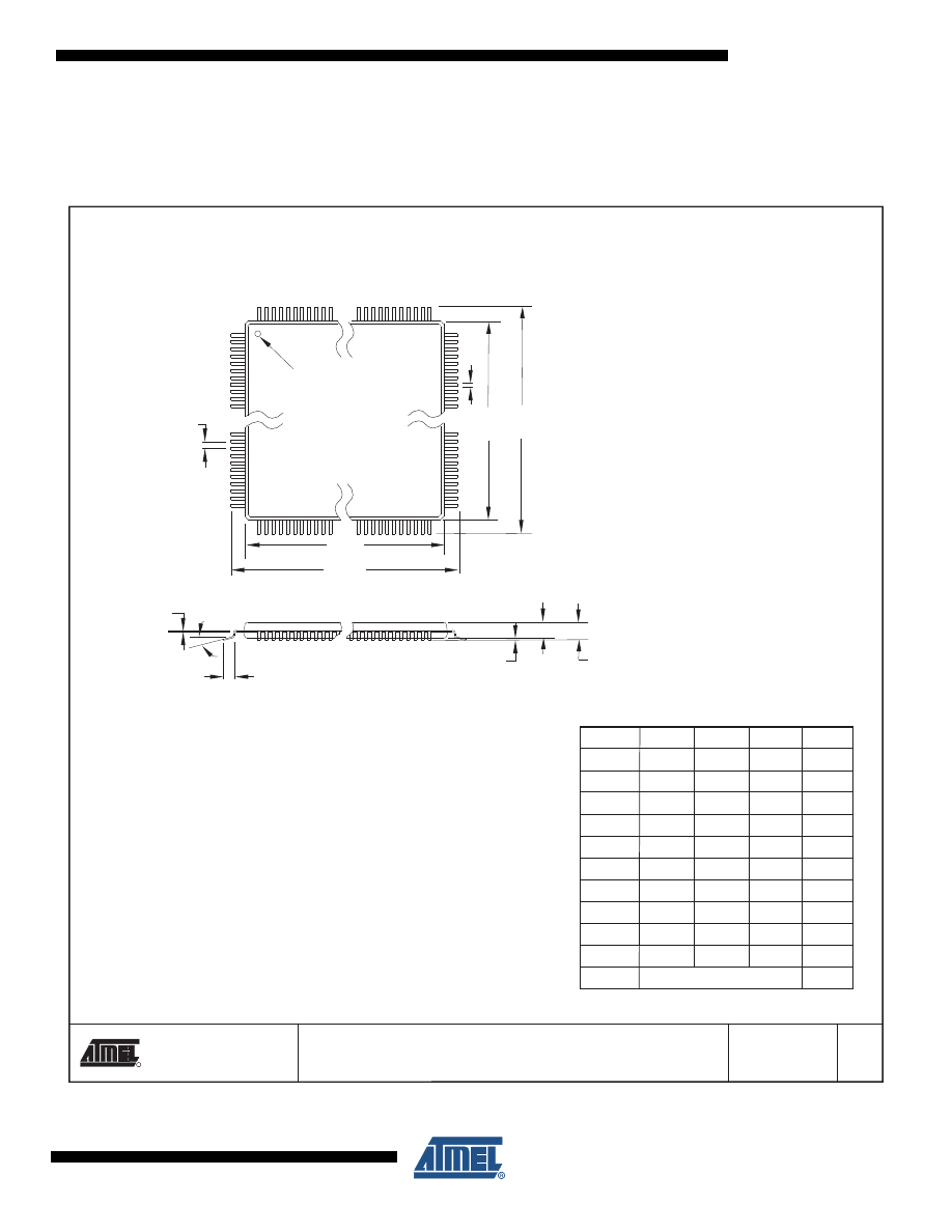
44A
44-lead, 10 x 10 x 1.0 mm, Thin Profile Plastic Quad Flat Package (TQFP)
40P6
40-pin, 0.600” Wide, Plastic Dual Inline Package (PDIP)
44M1
44-pad, 7 x 7 x 1.0 mm, Quad Flat No-Lead/Micro Lead Frame Package (QFN/MLF)
13
8155BS–AVR–07/09
ATmega32A
8.
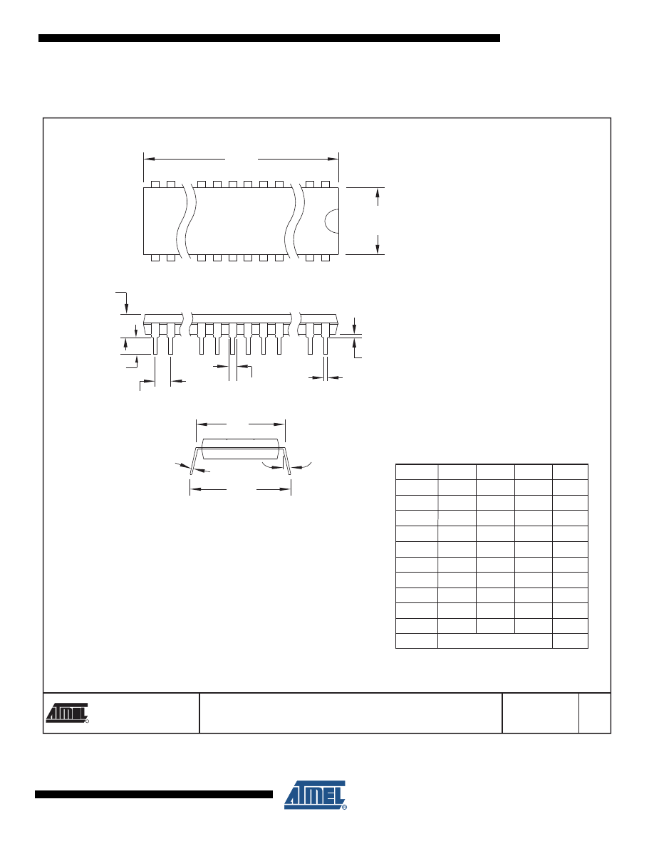
Packaging Information
8.1
44A
2325 Orchard Parkway
San Jose, CA 95131
TITLE
DRAWING NO.
R
REV.
44A, 44-lead, 10 x 10 mm Body Size, 1.0 mm Body Thickness,
0.8 mm Lead Pitch, Thin Profile Plastic Quad Flat Package (TQFP)
B
44A
10/5/2001
PIN 1 IDENTIFIER
0˚~7˚
PIN 1
L
C
A1
A2
A
D1
D
e
E1
E
B
COMMON DIMENSIONS
(Unit of Measure = mm)
SYMBOL
MIN
NOM
MAX
NOTE
Notes:
1. This package conforms to JEDEC reference MS-026, Variation ACB.
2. Dimensions D1 and E1 do not include mold protrusion. Allowable
protrusion is 0.25 mm per side. Dimensions D1 and E1 are maximum
plastic body size dimensions including mold mismatch.
3. Lead coplanarity is 0.10 mm maximum.
A
–
–
1.20
A1
0.05
–
0.15
A2
0.95
1.00
1.05
D
11.75
12.00
12.25
D1
9.90
10.00
10.10
Note 2
E
11.75
12.00
12.25
E1
9.90
10.00
10.10
Note 2
B 0.30
–
0.45
C
0.09
–
0.20
L
0.45
–
0.75
e
0.80 TYP
14
8155BS–AVR–07/09
ATmega32A
8.2
40P6
2325 Orchard Parkway
San Jose, CA 95131
TITLE
DRAWING NO.
R
REV.
40P6, 40-lead (0.600"/15.24 mm Wide) Plastic Dual
Inline Package (PDIP)
B
40P6
09/28/01
PIN
1
E1
A1
B
REF
E
B1
C
L
SEATING PLANE
A
0º ~ 15º
D
e
eB
COMMON DIMENSIONS
(Unit of Measure = mm)
SYMBOL
MIN
NOM
MAX
NOTE
A
–
–
4.826
A1
0.381
–
–
D
52.070
–
52.578
Note 2
E
15.240
–
15.875
E1
13.462
–
13.970
Note 2
B
0.356
–
0.559
B1
1.041
–
1.651
L
3.048
–
3.556
C
0.203
–
0.381
eB
15.494
–
17.526
e
2.540 TYP
Notes:
1. This package conforms to JEDEC reference MS-011, Variation AC.
2. Dimensions D and E1 do not include mold Flash or Protrusion.
Mold Flash or Protrusion shall not exceed 0.25 mm (0.010").
15
8155BS–AVR–07/09
ATmega32A
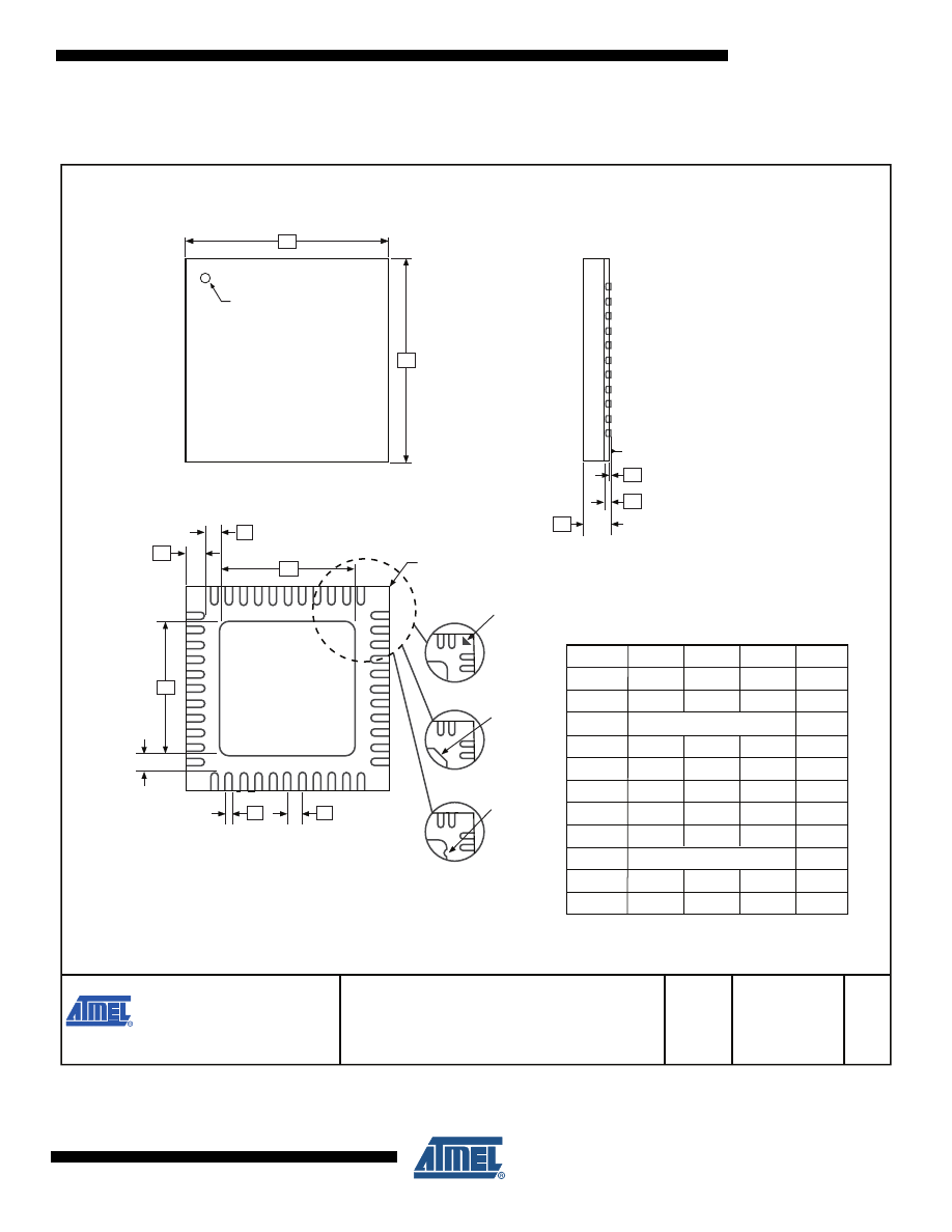
8.3
44M1
TITLE
DRAWING NO.
GPC
REV.
Package Drawing Contact:
packagedrawings@atmel.com
44M1
ZWS
H
44M1, 44-pad, 7 x 7 x 1.0 mm Body, Lead
Pitch 0.50 mm, 5.20 mm Exposed Pad, Thermally
Enhanced Plastic Very Thin Quad Flat No
Lead Package (VQFN)
9/26/08
COMMON DIMENSIONS
(Unit of Measure = mm)
SYMBOL
MIN
NOM
MAX
NOTE
A
0.80 0.90 1.00
A1
–
0.02
0.05
A3
0.20
REF
b 0.18
0.23
0.30
D
D2
5.00
5.20
5.40
6.90
7.00
7.10
6.90
7.00
7.10
E
E2
5.00
5.20
5.40
e
0.50 BSC
L
0.59
0.64
0.69
K
0.20
0.26
0.41
Note: JEDEC Standard MO-220, Fig. 1 (SAW Singulation) VKKD-3.
TOP VIEW
SIDE VIEW
BOTTOM VIEW
D
E
Marked Pin# 1 ID
E2
D2
b
e
Pin #1 Corner
L
A1
A3
A
SEATING PLANE
Pin #1
Triangle
Pin #1
Chamfer
(C 0.30)
Option A
Option B
Pin #1
Notch
(0.20 R)
Option C
K
K
1
2
3

16
8155BS–AVR–07/09
ATmega32A
9.
Errata
9.1
ATmega32A, rev. G to rev. I
•
First Analog Comparator conversion may be delayed
•
Interrupts may be lost when writing the timer registers in the asynchronous timer
•
IDCODE masks data from TDI input
•
Reading EEPROM by using ST or STS to set EERE bit triggers unexpected interrupt request.
1.
First Analog Comparator conversion may be delayed
If the device is powered by a slow rising V
CC
, the first Analog Comparator conversion will
take longer than expected on some devices.
Problem Fix/Workaround
When the device has been powered or reset, disable then enable theAnalog Comparator
before the first conversion.
2.
Interrupts may be lost when writing the timer registers in the asynchronous timer
The interrupt will be lost if a timer register that is synchronous timer clock is written when the
asynchronous Timer/Counter register (TCNTx) is 0x00.
Problem Fix/Workaround
Always check that the asynchronous Timer/Counter register neither have the value 0xFF nor
0x00 before writing to the asynchronous Timer Control Register (TCCRx), asynchronous
Timer Counter Register (TCNTx), or asynchronous Output Compare Register (OCRx).
3.
IDCODE masks data from TDI input
The JTAG instruction IDCODE is not working correctly. Data to succeeding devices are
replaced by all-ones during Update-DR.
Problem Fix / Workaround
– If ATmega32A is the only device in the scan chain, the problem is not visible.
– Select the Device ID Register of the ATmega32A by issuing the IDCODE instruction
or by entering the Test-Logic-Reset state of the TAP controller to read out the
contents of its Device ID Register and possibly data from succeeding devices of the
scan chain. Issue the BYPASS instruction to the ATmega32A while reading the
Device ID Registers of preceding devices of the boundary scan chain.
– If the Device IDs of all devices in the boundary scan chain must be captured
simultaneously, the ATmega32A must be the fist device in the chain.
4.
Reading EEPROM by using ST or STS to set EERE bit triggers unexpected interrupt
request.
Reading EEPROM by using the ST or STS command to set the EERE bit in the EECR reg-
ister triggers an unexpected EEPROM interrupt request.
Problem Fix / Workaround
Always use OUT or SBI to set EERE in EECR.

17
8155BS–AVR–07/09
ATmega32A
10. Datasheet Revision History
Please note that the referring page numbers in this section are referred to this document. The
referring revision in this section are referring to the document revision.
10.1
Rev. 8155B – 07/09
10.2
Rev. 8155A – 06/08
1. Updated
“Errata” on page 343
.
2.
Updated the last page with Atmel’s new addresses.
1.
Initial revision (Based on the ATmega32/L datasheet 2503N-AVR-06/08)
Changes done compared ATmega32/L datasheet 2503N-AVR-06/08:
- Updated description in
“Stack Pointer” on page 11
.
- All Electrical characteristics is moved to
“Electrical Characteristics” on page 296
.
- Register descriptions are moved to sub sections at the end of each chapter.
- Test limits of Reset Pull-up Resistor (R
RST
) in
“DC Characteristics” on page 296
.
- New graphs in
“Typical Characteristics” on page 306
.
- New
“Ordering Information” on page 339
.

8155BS–AVR–07/09
Headquarters
International
Atmel Corporation
2325 Orchard Parkway
San Jose, CA 95131
USA
Tel: 1(408) 441-0311
Fax: 1(408) 487-2600
Atmel Asia
Unit 1-5 & 16, 19/F
BEA Tower, Millennium City 5
418 Kwun Tong Road
Kwun Tong, Kowloon
Hong Kong
Tel: (852) 2245-6100
Fax: (852) 2722-1369
Atmel Europe
Le Krebs
8, Rue Jean-Pierre Timbaud
BP 309
78054 Saint-Quentin-en-
Yvelines Cedex
France
Tel: (33) 1-30-60-70-00
Fax: (33) 1-30-60-71-11
Atmel Japan
9F, Tonetsu Shinkawa Bldg.
1-24-8 Shinkawa
Chuo-ku, Tokyo 104-0033
Japan
Tel: (81) 3-3523-3551
Fax: (81) 3-3523-7581
Product Contact
Web Site
www.atmel.com
Technical Support
avr@atmel.com
Sales Contact
www.atmel.com/contacts
Literature Requests
www.atmel.com/literature
Disclaimer: The information in this document is provided in connection with Atmel products. No license, express or implied, by estoppel or otherwise, to any
intellectual property right is granted by this document or in connection with the sale of Atmel products. EXCEPT AS SET FORTH IN ATMEL’S TERMS AND CONDI-
TIONS OF SALE LOCATED ON ATMEL’S WEB SITE, ATMEL ASSUMES NO LIABILITY WHATSOEVER AND DISCLAIMS ANY EXPRESS, IMPLIED OR STATUTORY
WARRANTY RELATING TO ITS PRODUCTS INCLUDING, BUT NOT LIMITED TO, THE IMPLIED WARRANTY OF MERCHANTABILITY, FITNESS FOR A PARTICULAR
PURPOSE, OR NON-INFRINGEMENT. IN NO EVENT SHALL ATMEL BE LIABLE FOR ANY DIRECT, INDIRECT, CONSEQUENTIAL, PUNITIVE, SPECIAL OR INCIDEN-
TAL DAMAGES (INCLUDING, WITHOUT LIMITATION, DAMAGES FOR LOSS OF PROFITS, BUSINESS INTERRUPTION, OR LOSS OF INFORMATION) ARISING OUT OF
THE USE OR INABILITY TO USE THIS DOCUMENT, EVEN IF ATMEL HAS BEEN ADVISED OF THE POSSIBILITY OF SUCH DAMAGES. Atmel makes no
representations or warranties with respect to the accuracy or completeness of the contents of this document and reserves the right to make changes to specifications
and product descriptions at any time without notice. Atmel does not make any commitment to update the information contained herein. Unless specifically provided
otherwise, Atmel products are not suitable for, and shall not be used in, automotive applications. Atmel’s products are not intended, authorized, or warranted for use
as components in applications intended to support or sustain life.
© 2009 Atmel Corporation. All rights reserved. Atmel
®
, Atmel logo and combinations thereof, AVR
®
and others are registered trademarks or
trademarks of Atmel Corporation or its subsidiaries. Other terms and product names may be trademarks of others.
Document Outline
- Features
- 1. Pin Configurations
- 2. Overview
- 3. Resources
- 4. Data Retention
- 5. Register Summary
- 6. Instruction Set Summary
- 7. Ordering Information
- 8. Packaging Information
- 9. Errata
- 10. Datasheet Revision History
Wyszukiwarka
Podobne podstrony:
Atmega fusebit doctor (HVPP+HVSP) – napraw fusebity
ATmega16
ATMega8535 id 71672 Nieznany (2)
atmega16mmr
LCD ATMEGAlmc ssc2a16 03 1263
Atmega 8 opis
Zablokowana Atmega1, elektronika, mikroprocesory, Różne
ATmega8 vs ATmegaXX8
atmega8 panfi
06 atmega16
Porównanie Atmega8 Atmega8A Atmega88 Atmega88PA
AtMega32 AVRISP id 71658 Nieznany
atmega8 test board sciezki
atmega8 test board opis
atmega16a
atmega128 id 71652 Nieznany
atmega8 podsumowanie
więcej podobnych podstron