
Features
•
High-performance, Low-power AVR
®
8-bit Microcontroller
•
Advanced RISC Architecture
– 130 Powerful Instructions – Most Single-clock Cycle Execution
– 32 x 8 General Purpose Working Registers
– Fully Static Operation
– Up to 16 MIPS Throughput at 16 MHz
– On-chip 2-cycle Multiplier
•
High Endurance Non-volatile Memory segments
– 8K Bytes of In-System Self-programmable Flash program memory
– 512 Bytes EEPROM
– 1K Byte Internal SRAM
– Write/Erase Cycles: 10,000 Flash/100,000 EEPROM
– Data retention: 20 years at 85°C/100 years at 25°C
(1)
– Optional Boot Code Section with Independent Lock Bits
In-System Programming by On-chip Boot Program
True Read-While-Write Operation
– Programming Lock for Software Security
•
Peripheral Features
– Two 8-bit Timer/Counters with Separate Prescaler, one Compare Mode
– One 16-bit Timer/Counter with Separate Prescaler, Compare Mode, and Capture
Mode
– Real Time Counter with Separate Oscillator
– Three PWM Channels
– 8-channel ADC in TQFP and QFN/MLF package
Eight Channels 10-bit Accuracy
– 6-channel ADC in PDIP package
Six Channels 10-bit Accuracy
– Byte-oriented Two-wire Serial Interface
– Programmable Serial USART
– Master/Slave SPI Serial Interface
– Programmable Watchdog Timer with Separate On-chip Oscillator
– On-chip Analog Comparator
•
Special Microcontroller Features
– Power-on Reset and Programmable Brown-out Detection
– Internal Calibrated RC Oscillator
– External and Internal Interrupt Sources
– Five Sleep Modes: Idle, ADC Noise Reduction, Power-save, Power-down, and
Standby
•
I/O and Packages
– 23 Programmable I/O Lines
– 28-lead PDIP, 32-lead TQFP, and 32-pad QFN/MLF
•
Operating Voltages
– 2.7 - 5.5V (ATmega8L)
– 4.5 - 5.5V (ATmega8)
•
Speed Grades
– 0 - 8 MHz (ATmega8L)
– 0 - 16 MHz (ATmega8)
•
Power Consumption at 4 Mhz, 3V, 25
°C
– Active: 3.6 mA
– Idle Mode: 1.0 mA
– Power-down Mode: 0.5 µA
8-bit
with 8K Bytes
In-System
Programmable
Flash
ATmega8
ATmega8L
Summary
2
2486TS–AVR–05/08
ATmega8(L)
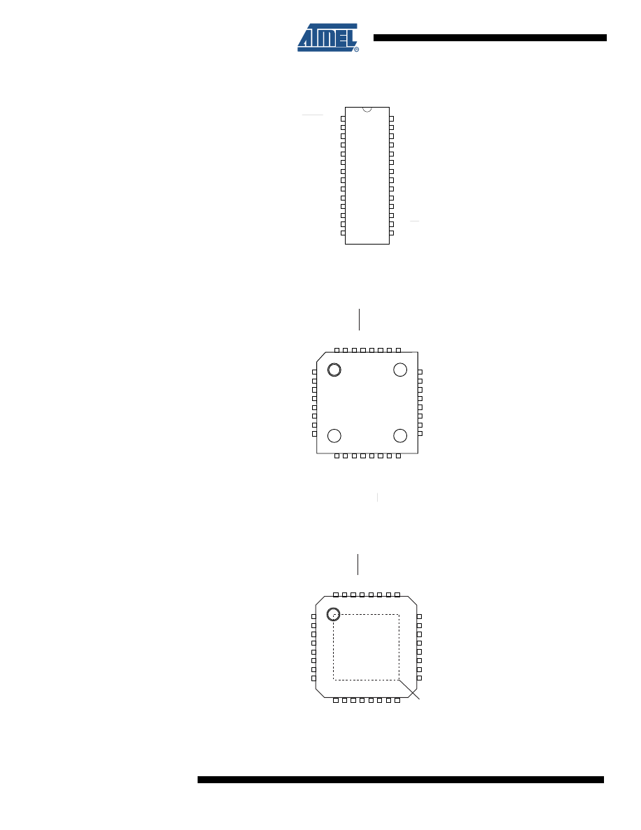
Pin
Configurations
1
2
3
4
5
6
7
8
24
23
22
21
20
19
18
17
(INT1) PD3
(XCK/T0) PD4
GND
VCC
GND
VCC
(XTAL1/TOSC1) PB6
(XTAL2/TOSC2) PB7
PC1 (ADC1)
PC0 (ADC0)
ADC7
GND
AREF
ADC6
AVCC
PB5 (SCK)
32
31
30
29
28
27
26
25
9
10
11
12
13
14
15
16
(T1) PD5
(AIN0) PD6
(AIN1) PD7
(ICP1) PB0
(OC1A) PB1
(SS/OC1B) PB2
(MOSI/OC2) PB3
(MISO) PB4
PD2 (INT0)
PD1 (TXD)
PD0 (RXD)
PC6 (RESET)
PC5 (ADC5/SCL)
PC4 (ADC4/SDA)
PC3 (ADC3)
PC2 (ADC2)
TQFP Top View
1
2
3
4
5
6
7
8
9
10
11
12
13
14
28
27
26
25
24
23
22
21
20
19
18
17
16
15
(RESET) PC6
(RXD) PD0
(TXD) PD1
(INT0) PD2
(INT1) PD3
(XCK/T0) PD4
VCC
GND
(XTAL1/TOSC1) PB6
(XTAL2/TOSC2) PB7
(T1) PD5
(AIN0) PD6
(AIN1) PD7
(ICP1) PB0
PC5 (ADC5/SCL)
PC4 (ADC4/SDA)
PC3 (ADC3)
PC2 (ADC2)
PC1 (ADC1)
PC0 (ADC0)
GND
AREF
AVCC
PB5 (SCK)
PB4 (MISO)
PB3 (MOSI/OC2)
PB2 (SS/OC1B)
PB1 (OC1A)
PDIP
1
2
3
4
5
6
7
8
24
23
22
21
20
19
18
17
32
31
30
29
28
27
26
25
9
10
11
12
13
14
15
16
MLF Top View
(INT1) PD3
(XCK/T0) PD4
GND
VCC
GND
VCC
(XTAL1/TOSC1) PB6
(XTAL2/TOSC2) PB7
PC1 (ADC1)
PC0 (ADC0)
ADC7
GND
AREF
ADC6
AVCC
PB5 (SCK)
(T1) PD5
(AIN0) PD6
(AIN1) PD7
(ICP1) PB0
(OC1A) PB1
(SS/OC1B) PB2
(MOSI/OC2) PB3
(MISO) PB4
PD2 (INT0)
PD1 (TXD)
PD0 (RXD)
PC6 (RESET)
PC5 (ADC5/SCL)
PC4 (ADC4/SDA)
PC3 (ADC3)
PC2 (ADC2)
NOTE:
The large center pad underneath the MLF
packages is made of metal and internally
connected to GND. It should be soldered
or glued to the PCB to ensure good
mechanical stability. If the center pad is
left unconneted, the package might
loosen from the PCB.
3
2486TS–AVR–05/08
ATmega8(L)
Overview
The ATmega8 is a low-power CMOS 8-bit microcontroller based on the AVR RISC architecture.
By executing powerful instructions in a single clock cycle, the ATmega8 achieves throughputs
approaching 1 MIPS per MHz, allowing the system designer to optimize power consumption ver-
sus processing speed.
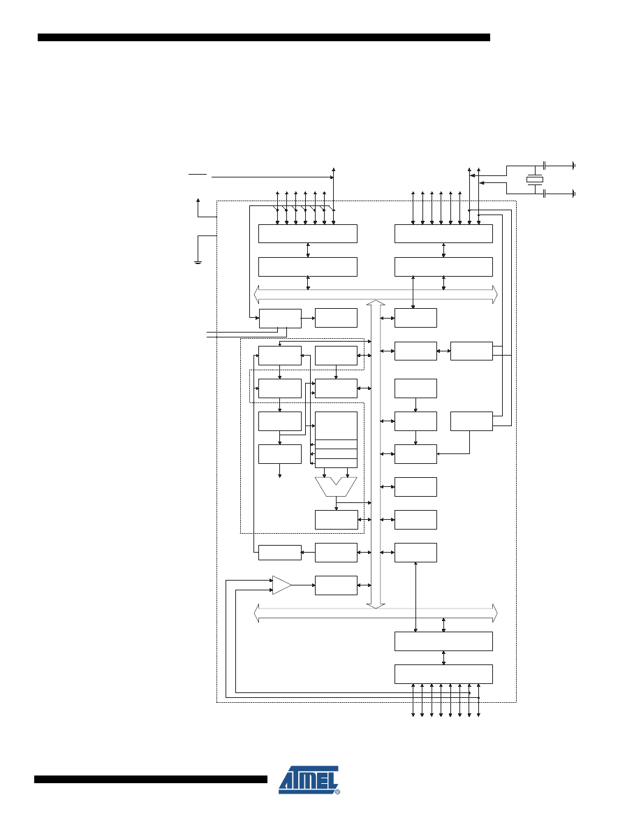
Block Diagram
Figure 1. Block Diagram
INTERNAL
OSCILLATOR
OSCILLATOR
WATCHDOG
TIMER
MCU CTRL.
& TIMING
OSCILLATOR
TIMERS/
COUNTERS
INTERRUPT
UNIT
STACK
POINTER
EEPROM
SRAM
STATUS
REGISTER
USART
PROGRAM
COUNTER
PROGRAM
FLASH
INSTRUCTION
REGISTER
INSTRUCTION
DECODER
PROGRAMMING
LOGIC
SPI
ADC
INTERFACE
COMP.
INTERFACE
PORTC DRIVERS/BUFFERS
PORTC DIGITAL INTERFACE
GENERAL
PURPOSE
REGISTERS
X
Y
Z
ALU
+
-
PORTB DRIVERS/BUFFERS
PORTB DIGITAL INTERFACE
PORTD DIGITAL INTERFACE
PORTD DRIVERS/BUFFERS
XTAL1
XTAL2
CONTROL
LINES
VCC
GND
MUX &
ADC
AGND
AREF
PC0 - PC6
PB0 - PB7
PD0 - PD7
AVR CPU
TWI
RESET

4
2486TS–AVR–05/08
ATmega8(L)
The AVR core combines a rich instruction set with 32 general purpose working registers. All the
32 registers are directly connected to the Arithmetic Logic Unit (ALU), allowing two independent
registers to be accessed in one single instruction executed in one clock cycle. The resulting
architecture is more code efficient while achieving throughputs up to ten times faster than con-
ventional CISC microcontrollers.
The ATmega8 provides the following features: 8K bytes of In-System Programmable Flash with
Read-While-Write capabilities, 512 bytes of EEPROM, 1K byte of SRAM, 23 general purpose
I/O lines, 32 general purpose working registers, three flexible Timer/Counters with compare
modes, internal and external interrupts, a serial programmable USART, a byte oriented Two-
wire Serial Interface, a 6-channel ADC (eight channels in TQFP and QFN/MLF packages) with
10-bit accuracy, a programmable Watchdog Timer with Internal Oscillator, an SPI serial port,
and five software selectable power saving modes. The Idle mode stops the CPU while allowing
the SRAM, Timer/Counters, SPI port, and interrupt system to continue functioning. The Power-
down mode saves the register contents but freezes the Oscillator, disabling all other chip func-
tions until the next Interrupt or Hardware Reset. In Power-save mode, the asynchronous timer
continues to run, allowing the user to maintain a timer base while the rest of the device is sleep-
ing. The ADC Noise Reduction mode stops the CPU and all I/O modules except asynchronous
timer and ADC, to minimize switching noise during ADC conversions. In Standby mode, the
crystal/resonator Oscillator is running while the rest of the device is sleeping. This allows very
fast start-up combined with low-power consumption.
The device is manufactured using Atmel’s high density non-volatile memory technology. The
Flash Program memory can be reprogrammed In-System through an SPI serial interface, by a
conventional non-volatile memory programmer, or by an On-chip boot program running on the
AVR core. The boot program can use any interface to download the application program in the
Application Flash memory. Software in the Boot Flash Section will continue to run while the
Application Flash Section is updated, providing true Read-While-Write operation. By combining
an 8-bit RISC CPU with In-System Self-Programmable Flash on a monolithic chip, the Atmel
ATmega8 is a powerful microcontroller that provides a highly-flexible and cost-effective solution
to many embedded control applications.
The ATmega8 AVR is supported with a full suite of program and system development tools,
including C compilers, macro assemblers, program debugger/simulators, In-Circuit Emulators,
and evaluation kits.
Disclaimer
Typical values contained in this datasheet are based on simulations and characterization of
other AVR microcontrollers manufactured on the same process technology. Min and Max values
will be available after the device is characterized.

5
2486TS–AVR–05/08
ATmega8(L)
Pin Descriptions
VCC
Digital supply voltage.
GND
Ground.
Port B (PB7..PB0)
XTAL1/XTAL2/TOSC1/
TOSC2
Port B is an 8-bit bi-directional I/O port with internal pull-up resistors (selected for each bit). The
Port B output buffers have symmetrical drive characteristics with both high sink and source
capability. As inputs, Port B pins that are externally pulled low will source current if the pull-up
resistors are activated. The Port B pins are tri-stated when a reset condition becomes active,
even if the clock is not running.
Depending on the clock selection fuse settings, PB6 can be used as input to the inverting Oscil-
lator amplifier and input to the internal clock operating circuit.
Depending on the clock selection fuse settings, PB7 can be used as output from the inverting
Oscillator amplifier.
If the Internal Calibrated RC Oscillator is used as chip clock source, PB7..6 is used as TOSC2..1
input for the Asynchronous Timer/Counter2 if the AS2 bit in ASSR is set.
The various special features of Port B are elaborated in
“Alternate Functions of Port B” on page
58
and
“System Clock and Clock Options” on page 25
.
Port C (PC5..PC0)
Port C is an 7-bit bi-directional I/O port with internal pull-up resistors (selected for each bit). The
Port C output buffers have symmetrical drive characteristics with both high sink and source
capability. As inputs, Port C pins that are externally pulled low will source current if the pull-up
resistors are activated. The Port C pins are tri-stated when a reset condition becomes active,
even if the clock is not running.
PC6/RESET
If the RSTDISBL Fuse is programmed, PC6 is used as an I/O pin. Note that the electrical char-
acteristics of PC6 differ from those of the other pins of Port C.
If the RSTDISBL Fuse is unprogrammed, PC6 is used as a Reset input. A low level on this pin
for longer than the minimum pulse length will generate a Reset, even if the clock is not running.
The minimum pulse length is given in
Table 15 on page 38
. Shorter pulses are not guaranteed to
generate a Reset.
The various special features of Port C are elaborated on
page 61
.
Port D (PD7..PD0)
Port D is an 8-bit bi-directional I/O port with internal pull-up resistors (selected for each bit). The
Port D output buffers have symmetrical drive characteristics with both high sink and source
capability. As inputs, Port D pins that are externally pulled low will source current if the pull-up
resistors are activated. The Port D pins are tri-stated when a reset condition becomes active,
even if the clock is not running.
Port D also serves the functions of various special features of the ATmega8 as listed on
page
63
.
RESET
Reset input. A low level on this pin for longer than the minimum pulse length will generate a
reset, even if the clock is not running. The minimum pulse length is given in
Table 15 on page
38
. Shorter pulses are not guaranteed to generate a reset.

6
2486TS–AVR–05/08
ATmega8(L)
AV
CC
AV
CC
is the supply voltage pin for the A/D Converter, Port C (3..0), and ADC (7..6). It should be
externally connected to V
CC
, even if the ADC is not used. If the ADC is used, it should be con-
nected to V
CC
through a low-pass filter. Note that Port C (5..4) use digital supply voltage, V
CC
.
AREF
AREF is the analog reference pin for the A/D Converter.
ADC7..6 (TQFP and
QFN/MLF Package
Only)
In the TQFP and QFN/MLF package, ADC7..6 serve as analog inputs to the A/D converter.
These pins are powered from the analog supply and serve as 10-bit ADC channels.

7
2486TS–AVR–05/08
ATmega8(L)
Resources
A comprehensive set of development tools, application notes and datasheets are available for
download on http://www.atmel.com/avr.
Note:
1.
Data Retention
Reliability Qualification results show that the projected data retention failure rate is much less
than 1 PPM over 20 years at 85°C or 100 years at 25°C.
8
2486TS–AVR–05/08
ATmega8(L)
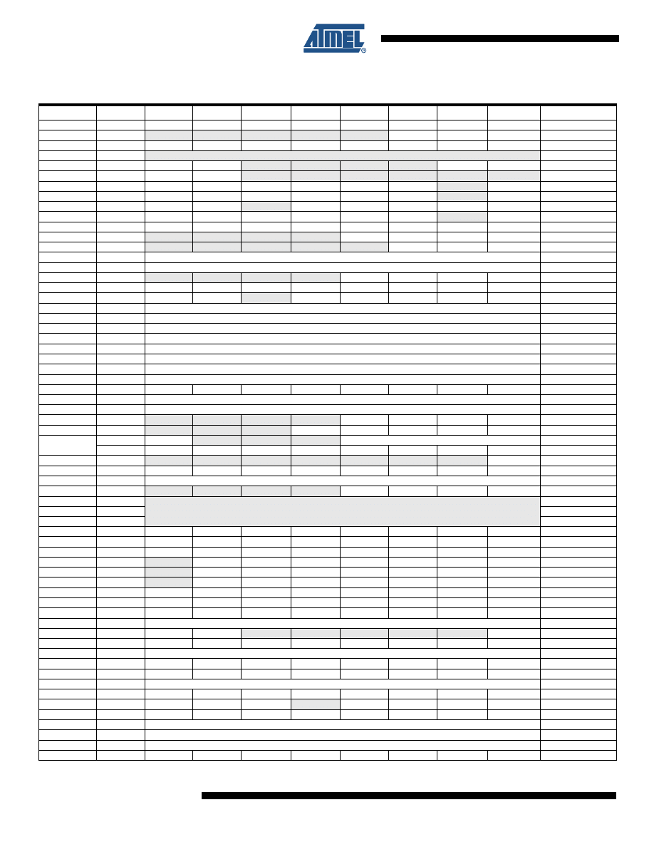
Register Summary
Address
Name
Bit 7
Bit 6
Bit 5
Bit 4
Bit 3
Bit 2
Bit 1
Bit 0
Page
0x3F (0x5F)
SREG
I
T
H
S
V
N
Z
C
11
0x3E (0x5E)
SPH
–
–
–
–
–
SP10
SP9
SP8
13
0x3D (0x5D)
SPL
SP7
SP6
SP5
SP4
SP3
SP2
SP1
SP0
13
0x3C (0x5C)
Reserved
0x3B (0x5B)
GICR
INT1
INT0
–
–
–
–
IVSEL
IVCE
49, 67
0x3A (0x5A)
GIFR
INTF1
INTF0
–
–
–
–
–
–
68
0x39 (0x59)
TIMSK
OCIE2
TOIE2
TICIE1
OCIE1A
OCIE1B
TOIE1
–
TOIE0
72, 102, 122
0x38 (0x58)
TIFR
OCF2
TOV2
ICF1
OCF1A
OCF1B
TOV1
–
TOV0
73, 102, 122
0x37 (0x57)
SPMCR
SPMIE
RWWSB
–
RWWSRE
BLBSET
PGWRT
PGERS
SPMEN
213
0x36 (0x56)
TWCR
TWINT
TWEA
TWSTA
TWSTO
TWWC
TWEN
–
TWIE
171
0x35 (0x55)
MCUCR
SE
SM2
SM1
SM0
ISC11
ISC10
ISC01
ISC00
33, 66
0x34 (0x54)
MCUCSR
–
–
–
–
WDRF
BORF
EXTRF
PORF
41
0x33 (0x53)
TCCR0
–
–
–
–
–
CS02
CS01
CS00
72
0x32 (0x52)
TCNT0
Timer/Counter0 (8 Bits)
72
0x31 (0x51)
OSCCAL
Oscillator Calibration Register
31
0x30 (0x50)
SFIOR
–
–
–
–
ACME
PUD
PSR2
PSR10
58, 75, 123, 193
0x2F (0x4F)
TCCR1A
COM1A1
COM1A0
COM1B1
COM1B0
FOC1A
FOC1B
WGM11
WGM10
96
0x2E (0x4E)
TCCR1B
ICNC1
ICES1
–
WGM13
WGM12
CS12
CS11
CS10
100
0x2D (0x4D)
TCNT1H
Timer/Counter1 – Counter Register High byte
101
0x2C (0x4C)
TCNT1L
Timer/Counter1 – Counter Register Low byte
101
0x2B (0x4B)
OCR1AH
Timer/Counter1 – Output Compare Register A High byte
101
0x2A (0x4A)
OCR1AL
Timer/Counter1 – Output Compare Register A Low byte
101
0x29 (0x49)
OCR1BH
Timer/Counter1 – Output Compare Register B High byte
101
0x28 (0x48)
OCR1BL
Timer/Counter1 – Output Compare Register B Low byte
101
0x27 (0x47)
ICR1H
Timer/Counter1 – Input Capture Register High byte
102
0x26 (0x46)
ICR1L
Timer/Counter1 – Input Capture Register Low byte
102
0x25 (0x45)
TCCR2
FOC2
WGM20
COM21
COM20
WGM21
CS22
CS21
CS20
117
0x24 (0x44)
TCNT2
Timer/Counter2 (8 Bits)
119
0x23 (0x43)
OCR2
Timer/Counter2 Output Compare Register
119
0x22 (0x42)
ASSR
–
–
–
–
AS2
TCN2UB
OCR2UB
TCR2UB
119
0x21 (0x41)
WDTCR
–
–
–
WDCE
WDE
WDP2
WDP1
WDP0
43
0x20
(1)
(0x40)
(1)
UBRRH
URSEL
–
–
–
UBRR[11:8]
158
UCSRC
URSEL
UMSEL
UPM1
UPM0
USBS
UCSZ1
UCSZ0
UCPOL
156
0x1F (0x3F)
EEARH
–
–
–
–
–
–
–
EEAR8
20
0x1E (0x3E)
EEARL
EEAR7
EEAR6
EEAR5
EEAR4
EEAR3
EEAR2
EEAR1
EEAR0
20
0x1D (0x3D)
EEDR
EEPROM Data Register
20
0x1C (0x3C)
EECR
–
–
–
–
EERIE
EEMWE
EEWE
EERE
20
0x1B (0x3B)
Reserved
0x1A (0x3A)
Reserved
0x19 (0x39)
Reserved
0x18 (0x38)
PORTB
PORTB7
PORTB6
PORTB5
PORTB4
PORTB3
PORTB2
PORTB1
PORTB0
65
0x17 (0x37)
DDRB
DDB7
DDB6
DDB5
DDB4
DDB3
DDB2
DDB1
DDB0
65
0x16 (0x36)
PINB
PINB7
PINB6
PINB5
PINB4
PINB3
PINB2
PINB1
PINB0
65
0x15 (0x35)
PORTC
–
PORTC6
PORTC5
PORTC4
PORTC3
PORTC2
PORTC1
PORTC0
65
0x14 (0x34)
DDRC
–
DDC6
DDC5
DDC4
DDC3
DDC2
DDC1
DDC0
65
0x13 (0x33)
PINC
–
PINC6
PINC5
PINC4
PINC3
PINC2
PINC1
PINC0
65
0x12 (0x32)
PORTD
PORTD7
PORTD6
PORTD5
PORTD4
PORTD3
PORTD2
PORTD1
PORTD0
65
0x11 (0x31)
DDRD
DDD7
DDD6
DDD5
DDD4
DDD3
DDD2
DDD1
DDD0
65
0x10 (0x30)
PIND
PIND7
PIND6
PIND5
PIND4
PIND3
PIND2
PIND1
PIND0
65
0x0F (0x2F)
SPDR
SPI Data Register
131
0x0E (0x2E)
SPSR
SPIF
WCOL
–
–
–
–
–
SPI2X
131
0x0D (0x2D)
SPCR
SPIE
SPE
DORD
MSTR
CPOL
CPHA
SPR1
SPR0
129
0x0C (0x2C)
UDR
USART I/O Data Register
153
0x0B (0x2B)
UCSRA
RXC
TXC
UDRE
FE
DOR
PE
U2X
MPCM
154
0x0A (0x2A)
UCSRB
RXCIE
TXCIE
UDRIE
RXEN
TXEN
UCSZ2
RXB8
TXB8
155
0x09 (0x29)
UBRRL
USART Baud Rate Register Low byte
158
0x08 (0x28)
ACSR
ACD
ACBG
ACO
ACI
ACIE
ACIC
ACIS1
ACIS0
194
0x07 (0x27)
ADMUX
REFS1
REFS0
ADLAR
–
MUX3
MUX2
MUX1
MUX0
205
0x06 (0x26)
ADCSRA
ADEN
ADSC
ADFR
ADIF
ADIE
ADPS2
ADPS1
ADPS0
207
0x05 (0x25)
ADCH
ADC Data Register High byte
208
0x04 (0x24)
ADCL
ADC Data Register Low byte
208
0x03 (0x23)
TWDR
Two-wire Serial Interface Data Register
173
0x02 (0x22)
TWAR
TWA6
TWA5
TWA4
TWA3
TWA2
TWA1
TWA0
TWGCE
174

9
2486TS–AVR–05/08
ATmega8(L)
Notes:
1. Refer to the USART description for details on how to access UBRRH and UCSRC.
2. For compatibility with future devices, reserved bits should be written to zero if accessed. Reserved I/O memory addresses
should never be written.
3. Some of the Status Flags are cleared by writing a logical one to them. Note that the CBI and SBI instructions will operate on
all bits in the I/O Register, writing a one back into any flag read as set, thus clearing the flag. The CBI and SBI instructions
work with registers 0x00 to 0x1F only.
0x01 (0x21)
TWSR
TWS7
TWS6
TWS5
TWS4
TWS3
–
TWPS1
TWPS0
173
0x00 (0x20)
TWBR
Two-wire Serial Interface Bit Rate Register
171
Register Summary (Continued)
Address
Name
Bit 7
Bit 6
Bit 5
Bit 4
Bit 3
Bit 2
Bit 1
Bit 0
Page
10
2486TS–AVR–05/08
ATmega8(L)
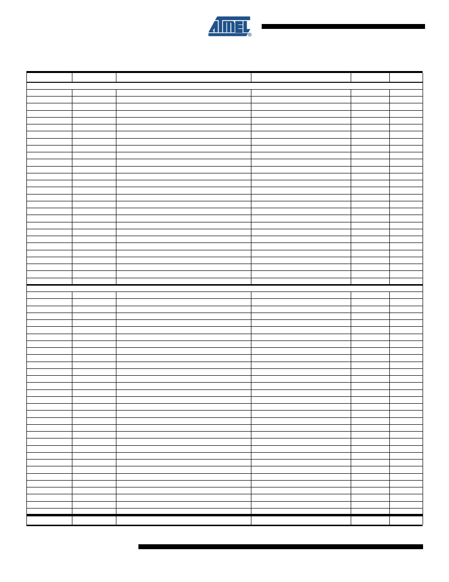
Instruction Set Summary
Mnemonics
Operands
Description
Operation
Flags
#Clocks
ARITHMETIC AND LOGIC INSTRUCTIONS
ADD
Rd, Rr
Add two Registers
Rd
← Rd + Rr
Z,C,N,V,H
1
ADC
Rd, Rr
Add with Carry two Registers
Rd
← Rd + Rr + C
Z,C,N,V,H
1
ADIW
Rdl,K
Add Immediate to Word
Rdh:Rdl
← Rdh:Rdl + K
Z,C,N,V,S
2
SUB
Rd, Rr
Subtract two Registers
Rd
← Rd - Rr
Z,C,N,V,H
1
SUBI
Rd, K
Subtract Constant from Register
Rd
← Rd - K
Z,C,N,V,H
1
SBC
Rd, Rr
Subtract with Carry two Registers
Rd
← Rd - Rr - C
Z,C,N,V,H
1
SBCI
Rd, K
Subtract with Carry Constant from Reg.
Rd
← Rd - K - C
Z,C,N,V,H
1
SBIW
Rdl,K
Subtract Immediate from Word
Rdh:Rdl
← Rdh:Rdl - K
Z,C,N,V,S
2
AND
Rd, Rr
Logical AND Registers
Rd
← Rd • Rr
Z,N,V
1
ANDI
Rd, K
Logical AND Register and Constant
Rd
← Rd • K
Z,N,V
1
OR
Rd, Rr
Logical OR Registers
Rd
← Rd v Rr
Z,N,V
1
ORI
Rd, K
Logical OR Register and Constant
Rd
← Rd v K
Z,N,V
1
EOR
Rd, Rr
Exclusive OR Registers
Rd
← Rd ⊕ Rr
Z,N,V
1
COM
Rd
One’s Complement
Rd
← 0xFF − Rd
Z,C,N,V
1
NEG
Rd
Two’s Complement
Rd
← 0x00 − Rd
Z,C,N,V,H
1
SBR
Rd,K
Set Bit(s) in Register
Rd
← Rd v K
Z,N,V
1
CBR
Rd,K
Clear Bit(s) in Register
Rd
← Rd • (0xFF - K)
Z,N,V
1
INC
Rd
Increment
Rd
← Rd + 1
Z,N,V
1
DEC
Rd
Decrement
Rd
← Rd − 1
Z,N,V
1
TST
Rd
Test for Zero or Minus
Rd
← Rd • Rd
Z,N,V
1
CLR
Rd
Clear Register
Rd
← Rd ⊕ Rd
Z,N,V
1
SER
Rd
Set Register
Rd
← 0xFF
None
1
MUL
Rd, Rr
Multiply Unsigned
R1:R0
← Rd x Rr
Z,C
2
MULS
Rd, Rr
Multiply Signed
R1:R0
← Rd x Rr
Z,C
2
MULSU
Rd, Rr
Multiply Signed with Unsigned
R1:R0
← Rd x Rr
Z,C
2
FMUL
Rd, Rr
Fractional Multiply Unsigned
R1:R0
← (Rd x Rr)
<< 1
Z,C
2
FMULS
Rd, Rr
Fractional Multiply Signed
R1:R0
← (Rd x Rr)
<< 1
Z,C
2
FMULSU
Rd, Rr
Fractional Multiply Signed with Unsigned
R1:R0
← (Rd x Rr)
<< 1
Z,C
2
BRANCH INSTRUCTIONS
RJMP
k
Relative Jump
PC
← PC + k + 1
None
2
IJMP
Indirect Jump to (Z)
PC
← Z
None
2
RCALL
k
Relative Subroutine Call
PC
← PC + k + 1
None
3
ICALL
Indirect Call to (Z)
PC
← Z
None
3
RET
Subroutine Return
PC
← STACK
None
4
RETI
Interrupt Return
PC
← STACK
I
4
CPSE
Rd,Rr
Compare, Skip if Equal
if (Rd = Rr) PC
← PC + 2 or 3
None
1 / 2 / 3
CP
Rd,Rr
Compare
Rd
− Rr
Z, N,V,C,H
1
CPC
Rd,Rr
Compare with Carry
Rd
− Rr − C
Z, N,V,C,H
1
CPI
Rd,K
Compare Register with Immediate
Rd
− K
Z, N,V,C,H
1
SBRC
Rr, b
Skip if Bit in Register Cleared
if (Rr(b)=0) PC
← PC + 2 or 3
None
1 / 2 / 3
SBRS
Rr, b
Skip if Bit in Register is Set
if (Rr(b)=1) PC
← PC + 2 or 3
None
1 / 2 / 3
SBIC
P, b
Skip if Bit in I/O Register Cleared
if (P(b)=0) PC
← PC + 2 or 3
None
1 / 2 / 3
SBIS
P, b
Skip if Bit in I/O Register is Set
if (P(b)=1) PC
← PC + 2 or 3
None
1 / 2 / 3
BRBS
s, k
Branch if Status Flag Set
if (SREG(s) = 1) then PC
←PC+k + 1
None
1 / 2
BRBC
s, k
Branch if Status Flag Cleared
if (SREG(s) = 0) then PC
←PC+k + 1
None
1 / 2
BREQ
k
Branch if Equal
if (Z = 1) then PC
← PC + k + 1
None
1 / 2
BRNE
k
Branch if Not Equal
if (Z = 0) then PC
← PC + k + 1
None
1 / 2
BRCS
k
Branch if Carry Set
if (C = 1) then PC
← PC + k + 1
None
1 / 2
BRCC
k
Branch if Carry Cleared
if (C = 0) then PC
← PC + k + 1
None
1 / 2
BRSH
k
Branch if Same or Higher
if (C = 0) then PC
← PC + k + 1
None
1 / 2
BRLO
k
Branch if Lower
if (C = 1) then PC
← PC + k + 1
None
1 / 2
BRMI
k
Branch if Minus
if (N = 1) then PC
← PC + k + 1
None
1 / 2
BRPL
k
Branch if Plus
if (N = 0) then PC
← PC + k + 1
None
1 / 2
BRGE
k
Branch if Greater or Equal, Signed
if (N
⊕ V= 0) then PC ← PC + k + 1
None
1 / 2
BRLT
k
Branch if Less Than Zero, Signed
if (N
⊕ V= 1) then PC ← PC + k + 1
None
1 / 2
BRHS
k
Branch if Half Carry Flag Set
if (H = 1) then PC
← PC + k + 1
None
1 / 2
BRHC
k
Branch if Half Carry Flag Cleared
if (H = 0) then PC
← PC + k + 1
None
1 / 2
BRTS
k
Branch if T Flag Set
if (T = 1) then PC
← PC + k + 1
None
1 / 2
BRTC
k
Branch if T Flag Cleared
if (T = 0) then PC
← PC + k + 1
None
1 / 2
BRVS
k
Branch if Overflow Flag is Set
if (V = 1) then PC
← PC + k + 1
None
1 / 2
BRVC
k
Branch if Overflow Flag is Cleared
if (V = 0) then PC
← PC + k + 1
None
1 / 2
Mnemonics
Operands
Description
Operation
Flags
#Clocks
11
2486TS–AVR–05/08
ATmega8(L)
BRIE
k
Branch if Interrupt Enabled
if ( I = 1) then PC
← PC + k + 1
None
1 / 2
BRID
k
Branch if Interrupt Disabled
if ( I = 0) then PC
← PC + k + 1
None
1 / 2
DATA TRANSFER INSTRUCTIONS
MOV
Rd, Rr
Move Between Registers
Rd
← Rr
None
1
MOVW
Rd, Rr
Copy Register Word
Rd+1:Rd
← Rr+1:Rr
None
1
LDI
Rd, K
Load Immediate
Rd
← K
None
1
LD
Rd, X
Load Indirect
Rd
← (X)
None
2
LD
Rd, X+
Load Indirect and Post-Inc.
Rd
← (X), X ← X + 1
None
2
LD
Rd, - X
Load Indirect and Pre-Dec.
X
← X - 1, Rd ← (X)
None
2
LD
Rd, Y
Load Indirect
Rd
← (Y)
None
2
LD
Rd, Y+
Load Indirect and Post-Inc.
Rd
← (Y), Y ← Y + 1
None
2
LD
Rd, - Y
Load Indirect and Pre-Dec.
Y
← Y - 1, Rd ← (Y)
None
2
LDD
Rd,Y+q
Load Indirect with Displacement
Rd
← (Y + q)
None
2
LD
Rd, Z
Load Indirect
Rd
← (Z)
None
2
LD
Rd, Z+
Load Indirect and Post-Inc.
Rd
← (Z), Z ← Z+1
None
2
LD
Rd, -Z
Load Indirect and Pre-Dec.
Z
← Z - 1, Rd ← (Z)
None
2
LDD
Rd, Z+q
Load Indirect with Displacement
Rd
← (Z + q)
None
2
LDS
Rd, k
Load Direct from SRAM
Rd
← (k)
None
2
ST
X, Rr
Store Indirect
(X)
← Rr
None
2
ST
X+, Rr
Store Indirect and Post-Inc.
(X)
← Rr, X ← X + 1
None
2
ST
- X, Rr
Store Indirect and Pre-Dec.
X
← X - 1, (X) ← Rr
None
2
ST
Y, Rr
Store Indirect
(Y)
← Rr
None
2
ST
Y+, Rr
Store Indirect and Post-Inc.
(Y)
← Rr, Y ← Y + 1
None
2
ST
- Y, Rr
Store Indirect and Pre-Dec.
Y
← Y - 1, (Y) ← Rr
None
2
STD
Y+q,Rr
Store Indirect with Displacement
(Y + q)
← Rr
None
2
ST
Z, Rr
Store Indirect
(Z)
← Rr
None
2
ST
Z+, Rr
Store Indirect and Post-Inc.
(Z)
← Rr, Z ← Z + 1
None
2
ST
-Z, Rr
Store Indirect and Pre-Dec.
Z
← Z - 1, (Z) ← Rr
None
2
STD
Z+q,Rr
Store Indirect with Displacement
(Z + q)
← Rr
None
2
STS
k, Rr
Store Direct to SRAM
(k)
← Rr
None
2
LPM
Load Program Memory
R0
← (Z)
None
3
LPM
Rd, Z
Load Program Memory
Rd
← (Z)
None
3
LPM
Rd, Z+
Load Program Memory and Post-Inc
Rd
← (Z), Z ← Z+1
None
3
SPM
Store Program Memory
(Z)
← R1:R0
None
-
IN
Rd, P
In Port
Rd
← P
None
1
OUT
P, Rr
Out Port
P
← Rr
None
1
PUSH
Rr
Push Register on Stack
STACK
← Rr
None
2
POP
Rd
Pop Register from Stack
Rd
← STACK
None
2
BIT AND BIT-TEST INSTRUCTIONS
SBI
P,b
Set Bit in I/O Register
I/O(P,b)
← 1
None
2
CBI
P,b
Clear Bit in I/O Register
I/O(P,b)
← 0
None
2
LSL
Rd
Logical Shift Left
Rd(n+1)
← Rd(n), Rd(0) ← 0
Z,C,N,V
1
LSR
Rd
Logical Shift Right
Rd(n)
← Rd(n+1), Rd(7) ← 0
Z,C,N,V
1
ROL
Rd
Rotate Left Through Carry
Rd(0)
←C,Rd(n+1)← Rd(n),C←Rd(7)
Z,C,N,V
1
ROR
Rd
Rotate Right Through Carry
Rd(7)
←C,Rd(n)← Rd(n+1),C←Rd(0)
Z,C,N,V
1
ASR
Rd
Arithmetic Shift Right
Rd(n)
← Rd(n+1), n=0..6
Z,C,N,V
1
SWAP
Rd
Swap Nibbles
Rd(3..0)
←Rd(7..4),Rd(7..4)←Rd(3..0)
None
1
BSET
s
Flag Set
SREG(s)
← 1
SREG(s)
1
BCLR
s
Flag Clear
SREG(s)
← 0
SREG(s)
1
BST
Rr, b
Bit Store from Register to T
T
← Rr(b)
T
1
BLD
Rd, b
Bit load from T to Register
Rd(b)
← T
None
1
SEC
Set Carry
C
← 1
C
1
CLC
Clear Carry
C
← 0
C
1
SEN
Set Negative Flag
N
← 1
N
1
CLN
Clear Negative Flag
N
← 0
N
1
SEZ
Set Zero Flag
Z
← 1
Z
1
CLZ
Clear Zero Flag
Z
← 0
Z
1
SEI
Global Interrupt Enable
I
← 1
I
1
CLI
Global Interrupt Disable
I
← 0
I
1
SES
Set Signed Test Flag
S
← 1
S
1
CLS
Clear Signed Test Flag
S
← 0
S
1
SEV
Set Twos Complement Overflow.
V
← 1
V
1
CLV
Clear Twos Complement Overflow
V
← 0
V
1
SET
Set T in SREG
T
← 1
T
1
Mnemonics
Operands
Description
Operation
Flags
#Clocks
Instruction Set Summary (Continued)

12
2486TS–AVR–05/08
ATmega8(L)
CLT
Clear T in SREG
T
← 0
T
1
SEH
Set Half Carry Flag in SREG
H
← 1
H
1
CLH
Clear Half Carry Flag in SREG
H
← 0
H
1
MCU CONTROL INSTRUCTIONS
NOP
No Operation
None
1
SLEEP
Sleep
(see specific descr. for Sleep function)
None
1
WDR
Watchdog Reset
(see specific descr. for WDR/timer)
None
1
Instruction Set Summary (Continued)
13
2486TS–AVR–05/08
ATmega8(L)
Ordering Information
Notes:
1. This device can also be supplied in wafer form. Please contact your local Atmel sales office for detailed ordering information
and minimum quantities.
2. Pb-free packaging complies to the European Directive for Restriction of Hazardous Substances (RoHS directive). Also
Halide free and fully Green.
Speed (MHz)
Power Supply
Ordering Code
Package
(1)
Operation Range
8
2.7 - 5.5
ATmega8L-8AU
(2)
ATmega8L-8PU
(2)
ATmega8L-8MU
(2)
32A
28P3
32M1-A
Industrial
(-40
°
C to 85
°
C)
16
4.5 - 5.5
ATmega8-16AU
(2)
ATmega8-16PU
(2)
ATmega8-16MU
(2)
32A
28P3
32M1-A
Industrial
(-40
°
C to 85
°
C)
Package Type
32A
32-lead, Thin (1.0 mm) Plastic Quad Flat Package (TQFP)
28P3
28-lead, 0.300” Wide, Plastic Dual Inline Package (PDIP)
32M1-A
32-pad, 5 x 5 x 1.0 body, Lead Pitch 0.50 mm Quad Flat No-Lead/Micro Lead Frame Package (QFN/MLF)
14
2486TS–AVR–05/08
ATmega8(L)
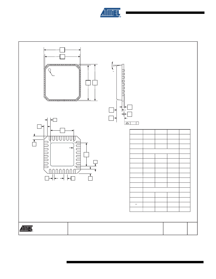
Packaging Information
32A
2325 Orchard Parkway
San Jose, CA 95131
TITLE
DRAWING NO.
R
REV.
32A, 32-lead, 7 x 7 mm Body Size, 1.0 mm Body Thickness,
0.8 mm Lead Pitch, Thin Profile Plastic Quad Flat Package (TQFP)
B
32A
10/5/2001
PIN 1 IDENTIFIER
0˚~7˚
PIN 1
L
C
A1
A2
A
D1
D
e
E1
E
B
Notes:
1. This package conforms to JEDEC reference MS-026, Variation ABA.
2. Dimensions D1 and E1 do not include mold protrusion. Allowable
protrusion is 0.25 mm per side. Dimensions D1 and E1 are maximum
plastic body size dimensions including mold mismatch.
3. Lead coplanarity is 0.10 mm maximum.
A
–
–
1.20
A1
0.05
–
0.15
A2
0.95
1.00
1.05
D
8.75
9.00
9.25
D1
6.90
7.00
7.10
Note 2
E
8.75
9.00
9.25
E1
6.90
7.00
7.10
Note 2
B 0.30
–
0.45
C
0.09
–
0.20
L
0.45
–
0.75
e
0.80 TYP
COMMON DIMENSIONS
(Unit of Measure = mm)
SYMBOL
MIN
NOM
MAX
NOTE
15
2486TS–AVR–05/08
ATmega8(L)
28P3
2325 Orchard Parkway
San Jose, CA 95131
TITLE
DRAWING NO.
R
REV.
28P3, 28-lead (0.300"/7.62 mm Wide) Plastic Dual
Inline Package (PDIP)
B
28P3
09/28/01
PIN
1
E1
A1
B
REF
E
B1
C
L
SEATING PLANE
A
0º ~ 15º
D
e
eB
B2
(4 PLACES)
COMMON DIMENSIONS
(Unit of Measure = mm)
SYMBOL
MIN
NOM
MAX
NOTE
A
–
–
4.5724
A1
0.508
–
–
D
34.544
– 34.798 Note 1
E
7.620
–
8.255
E1
7.112
–
7.493
Note 1
B
0.381
–
0.533
B1
1.143
–
1.397
B2
0.762
–
1.143
L
3.175
–
3.429
C
0.203
–
0.356
eB
–
–
10.160
e 2.540 TYP
Note:
1. Dimensions D and E1 do not include mold Flash or Protrusion.
Mold Flash or Protrusion shall not exceed 0.25 mm (0.010").
16
2486TS–AVR–05/08
ATmega8(L)
32M1-A
2325 Orchard Parkway
San Jose, CA 95131
TITLE
DRAWING NO.
R
REV.
32M1-A, 32-pad, 5 x 5 x 1.0 mm Body, Lead Pitch 0.50 mm,
E
32M1-A
5/25/06
3.10 mm Exposed Pad, Micro Lead Frame Package (MLF)
COMMON DIMENSIONS
(Unit of Measure = mm)
SYMBOL
MIN
NOM
MAX
NOTE
D1
D
E1
E
e
b
A3
A2
A1
A
D2
E2
0.08 C
L
1
2
3
P
P
0
1
2
3
A
0.80
0.90
1.00
A1
–
0.02
0.05
A2
–
0.65
1.00
A3
0.20 REF
b
0.18
0.23
0.30
D
D1
D2
2.95
3.10
3.25
4.90
5.00
5.10
4.70
4.75
4.80
4.70
4.75
4.80
4.90
5.00
5.10
E
E1
E2
2.95
3.10
3.25
e
0.50 BSC
L
0.30
0.40
0.50
P
–
–
0.60
–
–
12
o
Note: JEDEC Standard MO-220, Fig. 2 (Anvil Singulation), VHHD-2.
TOP VIEW
SIDE VIEW
BOTTOM VIEW
0
Pin 1 ID
Pin #1 Notch
(0.20 R)
K
0.20
–
–
K
K

17
2486TS–AVR–05/08
ATmega8(L)
Errata
The revision letter in this section refers to the revision of the ATmega8 device.
ATmega8
Rev. D to I
•
First Analog Comparator conversion may be delayed
•
Interrupts may be lost when writing the timer registers in the asynchronous timer
•
Signature may be Erased in Serial Programming Mode
•
CKOPT Does not Enable Internal Capacitors on XTALn/TOSCn Pins when 32 KHz Oscillator is
Used to Clock the Asynchronous Timer/Counter2
•
Reading EEPROM by using ST or STS to set EERE bit triggers unexpected interrupt request
1.
First Analog Comparator conversion may be delayed
If the device is powered by a slow rising V
CC
, the first Analog Comparator conversion will
take longer than expected on some devices.
Problem Fix / Workaround
When the device has been powered or reset, disable then enable theAnalog Comparator
before the first conversion.
2.
Interrupts may be lost when writing the timer registers in the asynchronous timer
If one of the timer registers which is synchronized to the asynchronous timer2 clock is writ-
ten in the cycle before a overflow interrupt occurs, the interrupt may be lost.
Problem Fix / Workaround
Always check that the Timer2 Timer/Counter register, TCNT2, does not have the value 0xFF
before writing the Timer2 Control Register, TCCR2, or Output Compare Register, OCR2
3.
Signature may be Erased in Serial Programming Mode
If the signature bytes are read before a chiperase command is completed, the signature may
be erased causing the device ID and calibration bytes to disappear. This is critical, espe-
cially, if the part is running on internal RC oscillator.
Problem Fix / Workaround:
Ensure that the chiperase command has exceeded before applying the next command.
4.
CKOPT Does not Enable Internal Capacitors on XTALn/TOSCn Pins when 32 KHz
Oscillator is Used to Clock the Asynchronous Timer/Counter2
When the internal RC Oscillator is used as the main clock source, it is possible to run the
Timer/Counter2 asynchronously by connecting a 32 KHz Oscillator between XTAL1/TOSC1
and XTAL2/TOSC2. But when the internal RC Oscillator is selected as the main clock
source, the CKOPT Fuse does not control the internal capacitors on XTAL1/TOSC1 and
XTAL2/TOSC2. As long as there are no capacitors connected to XTAL1/TOSC1 and
XTAL2/TOSC2, safe operation of the Oscillator is not guaranteed.
Problem Fix / Workaround
Use external capacitors in the range of 20 - 36 pF on XTAL1/TOSC1 and XTAL2/TOSC2.
This will be fixed in ATmega8 Rev. G where the CKOPT Fuse will control internal capacitors
also when internal RC Oscillator is selected as main clock source. For ATmega8 Rev. G,
CKOPT = 0 (programmed) will enable the internal capacitors on XTAL1 and XTAL2. Cus-
tomers who want compatibility between Rev. G and older revisions, must ensure that
CKOPT is unprogrammed (CKOPT = 1).
5.
Reading EEPROM by using ST or STS to set EERE bit triggers unexpected interrupt
request.
Reading EEPROM by using the ST or STS command to set the EERE bit in the EECR reg-
ister triggers an unexpected EEPROM interrupt request.

18
2486TS–AVR–05/08
ATmega8(L)
Problem Fix / Workaround
Always use OUT or SBI to set EERE in EECR.

19
2486TS–AVR–05/08
ATmega8(L)
Datasheet
Revision
History
Please note that the referring page numbers in this section are referred to this document. The
referring revision in this section are referring to the document revision.
Changes from Rev.
2486S- 08/07 to
Rev. 2486T- 05/08
1.
Updated
Table 98 on page 240
.
2.
Updated
“Ordering Information” on page 292
.
- Commercial Ordering Code removed.
- No Pb-free packaging option removed.
Changes from Rev.
2486R- 07/07 to
Rev. 2486S- 08/07
1.
Updated
“Features” on page 1
.
2.
Added
“Data Retention” on page 7
.
3.
Updated
“Errata” on page 17
.
4.
Updated
“Slave Mode” on page 129
.
Changes from Rev.
2486Q- 10/06 to
Rev. 2486R- 07/07
1.
Added text to
Table 81 on page 218
.
2.
Fixed typo in
“Peripheral Features” on page 1
.
3.
Updated
Table 16 on page 42
.
4.
Updated
Table 75 on page 206
.
5.
Removed redundancy and updated typo in Notes section of
“DC Characteristics” on
page 242
.
Changes from Rev.
2486P- 02/06 to
Rev. 2486Q- 10/06
1.
Updated
“Timer/Counter Oscillator” on page 32
.
2.
Updated
“Fast PWM Mode” on page 89
.
3.
Updated code example in
“USART Initialization” on page 138
.
4.
Updated
Table 37 on page 97
,
Table 39 on page 98
,
Table 42 on page 117
,
Table 44 on
page 118
, and
Table 98 on page 240
.
5.
Updated
“Errata” on page 17
.
Changes from Rev.
2486O-10/04 to
Rev. 2486P- 02/06
1.
Added
“Resources” on page 7
.
2.
Updated
“External Clock” on page 32
.
3.
Updated
“Serial Peripheral Interface – SPI” on page 124
.
4.
Updated Code Example in
“USART Initialization” on page 138
.

20
2486TS–AVR–05/08
ATmega8(L)
5.
Updated Note in
“Bit Rate Generator Unit” on page 170
.
6.
Updated
Table 98 on page 240
.
7.
Updated Note in
Table 103 on page 248
.
8.
Updated
“Errata” on page 17
.
Changes from Rev.
2486N-09/04 to
Rev. 2486O-10/04
1.
Removed to instances of “analog ground”. Replaced by “ground”.
2.
Updated
Table 7 on page 29
,
Table 15 on page 38
, and
Table 100 on page 244
.
3.
Updated
“Calibrated Internal RC Oscillator” on page 30
with the 1 MHz default value.
4.
Table 89 on page 225
and
Table 90 on page 225
moved to new section
“Page Size” on
page 225
.
5.
Updated descripton for bit 4 in
“Store Program Memory Control Register – SPMCR”
on page 213
.
6.
Updated
“Ordering Information” on page 13
.
Changes from Rev.
2486M-12/03 to
Rev. 2486N-09/04
1.
Added note to MLF package in
“Pin Configurations” on page 2
.
2.
Updated
“Internal Voltage Reference Characteristics” on page 42
.
3.
Updated
“DC Characteristics” on page 242
.
4.
ADC4 and ADC5 support 10-bit accuracy. Document updated to reflect this.
Updated features in
“Analog-to-Digital Converter” on page 196
.
Updated
“ADC Characteristics” on page 248
.
5.
Removed reference to “External RC Oscillator application note” from
“External RC
Oscillator” on page 28
.
Changes from Rev.
2486L-10/03 to
Rev. 2486M-12/03
1.
Updated
“Calibrated Internal RC Oscillator” on page 30
.
Changes from Rev.
2486K-08/03 to
Rev. 2486L-10/03
1.
Removed “Preliminary” and TBDs from the datasheet.
2.
Renamed ICP to ICP1 in the datasheet.
3.
Removed instructions CALL and JMP from the datasheet.
4.
Updated t
RST
in
Table 15 on page 38
, V
BG
in
Table 16 on page 42
,
Table 100 on page
244
and
Table 102 on page 246
.
5.
Replaced text “XTAL1 and XTAL2 should be left unconnected (NC)” after
Table 9
in
“Calibrated Internal RC Oscillator” on page 30
. Added text regarding XTAL1/XTAL2
and CKOPT Fuse in
“Timer/Counter Oscillator” on page 32
.

21
2486TS–AVR–05/08
ATmega8(L)
6.
Updated Watchdog Timer code examples in
“Timed Sequences for Changing the
Configuration of the Watchdog Timer” on page 45
.
7.
Removed bit 4, ADHSM, from
“Special Function IO Register – SFIOR” on page 58
.
8.
Added note 2 to
Figure 103 on page 215
.
9.
Updated item 4 in the
“Serial Programming Algorithm” on page 238
.
10. Added t
WD_FUSE
to
Table 97 on page 239
and updated Read Calibration Byte, Byte 3, in
Table 98 on page 240
.
11. Updated Absolute Maximum Ratings* and DC Characteristics in
“Electrical Character-
istics” on page 242
.
Changes from Rev.
2486J-02/03 to
Rev. 2486K-08/03
1.
Updated V
BOT
values in
Table 15 on page 38
.
2.
Updated
“ADC Characteristics” on page 248
.
3.
Updated
“ATmega8 Typical Characteristics” on page 249
.
4.
Updated
“Errata” on page 17
.
Changes from Rev.
2486I-12/02 to Rev.
2486J-02/03
1.
Improved the description of
“Asynchronous Timer Clock – clkASY” on page 26
.
2.
Removed reference to the “Multipurpose Oscillator” application note and the “32 kHz
Crystal Oscillator” application note, which do not exist.
3.
Corrected OCn waveforms in
Figure 38 on page 90
.
4.
Various minor Timer 1 corrections.
5.
Various minor TWI corrections.
6.
Added note under
“Filling the Temporary Buffer (Page Loading)” on page 216
about
writing to the EEPROM during an SPM Page load.
7.
Removed ADHSM completely.
8.
Added section
“EEPROM Write during Power-down Sleep Mode” on page 23
.
9.
Removed XTAL1 and XTAL2 description on
page 5
because they were already
described as part of
“Port B (PB7..PB0) XTAL1/XTAL2/TOSC1/TOSC2” on page 5
.
10. Improved the table under
“SPI Timing Characteristics” on page 246
and removed the
table under
“SPI Serial Programming Characteristics” on page 241
.
11. Corrected PC6 in
“Alternate Functions of Port C” on page 61
.
12. Corrected PB6 and PB7 in
“Alternate Functions of Port B” on page 58
.
13. Corrected 230.4 Mbps to 230.4 kbps under
“Examples of Baud Rate Setting” on page
159
.

22
2486TS–AVR–05/08
ATmega8(L)
14. Added information about PWM symmetry for Timer 2 in
“Phase Correct PWM Mode”
on page 113
.
15. Added thick lines around accessible registers in
Figure 76 on page 169
.
16. Changed “will be ignored” to “must be written to zero” for unused Z-pointer bits
under
“Performing a Page Write” on page 216
.
17. Added note for RSTDISBL Fuse in
Table 87 on page 223
.
18. Updated drawings in
“Packaging Information” on page 14
.
Changes from Rev.
2486H-09/02 to
Rev. 2486I-12/02
1.
Added errata for Rev D, E, and F on
page 17
.
Changes from Rev.
2486G-09/02 to
Rev. 2486H-09/02
1.
Changed the Endurance on the Flash to 10,000 Write/Erase Cycles.
Changes from Rev.
2486F-07/02 to
Rev. 2486G-09/02
1.
Updated
Table 103, “ADC Characteristics,” on page 248
.
Changes from Rev.
2486E-06/02 to
Rev. 2486F-07/02
1.
Changes in
“Digital Input Enable and Sleep Modes” on page 55
.
2.
Addition of OCS2 in
“MOSI/OC2 – Port B, Bit 3” on page 59
.
3.
The following tables have been updated:
Table 51, “CPOL and CPHA Functionality,” on page 132
,
Table 59, “UCPOL Bit Settings,”
on page 158
,
Table 72, “Analog Comparator Multiplexed Input(1),” on page 195
,
Table 73,
“ADC Conversion Time,” on page 200
,
Table 75, “Input Channel Selections,” on page 206
,
and
Table 84, “Explanation of Different Variables used in Figure 103 and the Mapping to the
Z-pointer,” on page 221
.
4.
Changes in
“Reading the Calibration Byte” on page 234
.
5.
Corrected Errors in Cross References.
Changes from Rev.
2486D-03/02 to
Rev. 2486E-06/02
1.
Updated Some Preliminary Test Limits and Characterization Data
The following tables have been updated:
Table 15, “Reset Characteristics,” on page 38
,
Table 16, “Internal Voltage Reference Char-
acteristics,” on page 42
, DC Characteristics on
page 242
,
Table , “ADC Characteristics,” on
page 248
.
2.
Changes in External Clock Frequency
Added the description at the end of
“External Clock” on page 32
.
Added period changing data in
Table 99, “External Clock Drive,” on page 244
.
3.
Updated TWI Chapter

23
2486TS–AVR–05/08
ATmega8(L)
More details regarding use of the TWI bit rate prescaler and a
Table 65, “TWI Bit Rate Pres-
caler,” on page 173
.
Changes from Rev.
2486C-03/02 to
Rev. 2486D-03/02
1.
Updated Typical Start-up Times.
The following tables has been updated:
Table 5, “Start-up Times for the Crystal Oscillator Clock Selection,” on page 28
,
Table 6,
“Start-up Times for the Low-frequency Crystal Oscillator Clock Selection,” on page 28
,
Table 8, “Start-up Times for the External RC Oscillator Clock Selection,” on page 29
, and
Table 12, “Start-up Times for the External Clock Selection,” on page 32
.
2.
Added
“ATmega8 Typical Characteristics” on page 249
.
Changes from Rev.
2486B-12/01 to
Rev. 2486C-03/02
1.
Updated TWI Chapter.
More details regarding use of the TWI Power-down operation and using the TWI as Master
with low TWBRR values are added into the datasheet.
Added the note at the end of the
“Bit Rate Generator Unit” on page 170
.
Added the description at the end of
“Address Match Unit” on page 170
.
2.
Updated Description of OSCCAL Calibration Byte.
In the datasheet, it was not explained how to take advantage of the calibration bytes for 2, 4,
and 8 MHz Oscillator selections. This is now added in the following sections:
Improved description of
“Oscillator Calibration Register – OSCCAL” on page 31
and
“Cali-
bration Byte” on page 225
.
3.
Added Some Preliminary Test Limits and Characterization Data.
Removed some of the TBD’s in the following tables and pages:
Table 3 on page 26
,
Table 15 on page 38
,
Table 16 on page 42
,
Table 17 on page 44
,
“TA =
-40×C to 85×C, VCC = 2.7V to 5.5V (unless otherwise noted)” on page 242
,
Table 99 on
page 244
, and
Table 102 on page 246
.
4.
Updated Programming Figures.
Figure 104 on page 226
and
Figure 112 on page 237
are updated to also reflect that AV
CC
must be connected during Programming mode.
5.
Added a Description on how to Enter Parallel Programming Mode if RESET Pin is Dis-
abled or if External Oscillators are Selected.
Added a note in section
“Enter Programming Mode” on page 228
.

2486TS–AVR–05/08
Headquarters
International
Atmel Corporation
2325 Orchard Parkway
San Jose, CA 95131
USA
Tel: 1(408) 441-0311
Fax: 1(408) 487-2600
Atmel Asia
Room 1219
Chinachem Golden Plaza
77 Mody Road Tsimshatsui
East Kowloon
Hong Kong
Tel: (852) 2721-9778
Fax: (852) 2722-1369
Atmel Europe
Le Krebs
8, Rue Jean-Pierre Timbaud
BP 309
78054 Saint-Quentin-en-
Yvelines Cedex
France
Tel: (33) 1-30-60-70-00
Fax: (33) 1-30-60-71-11
Atmel Japan
9F, Tonetsu Shinkawa Bldg.
1-24-8 Shinkawa
Chuo-ku, Tokyo 104-0033
Japan
Tel: (81) 3-3523-3551
Fax: (81) 3-3523-7581
Product Contact
Web Site
www.atmel.com
Technical Support
avr@atmel.com
Sales Contact
www.atmel.com/contacts
Literature Requests
www.atmel.com/literature
Disclaimer: The information in this document is provided in connection with Atmel products. No license, express or implied, by estoppel or otherwise, to any
intellectual property right is granted by this document or in connection with the sale of Atmel products. EXCEPT AS SET FORTH IN ATMEL’S TERMS AND CONDI-
TIONS OF SALE LOCATED ON ATMEL’S WEB SITE, ATMEL ASSUMES NO LIABILITY WHATSOEVER AND DISCLAIMS ANY EXPRESS, IMPLIED OR STATUTORY
WARRANTY RELATING TO ITS PRODUCTS INCLUDING, BUT NOT LIMITED TO, THE IMPLIED WARRANTY OF MERCHANTABILITY, FITNESS FOR A PARTICULAR
PURPOSE, OR NON-INFRINGEMENT. IN NO EVENT SHALL ATMEL BE LIABLE FOR ANY DIRECT, INDIRECT, CONSEQUENTIAL, PUNITIVE, SPECIAL OR INCIDEN-
TAL DAMAGES (INCLUDING, WITHOUT LIMITATION, DAMAGES FOR LOSS OF PROFITS, BUSINESS INTERRUPTION, OR LOSS OF INFORMATION) ARISING OUT OF
THE USE OR INABILITY TO USE THIS DOCUMENT, EVEN IF ATMEL HAS BEEN ADVISED OF THE POSSIBILITY OF SUCH DAMAGES. Atmel makes no
representations or warranties with respect to the accuracy or completeness of the contents of this document and reserves the right to make changes to specifications
and product descriptions at any time without notice. Atmel does not make any commitment to update the information contained herein. Unless specifically provided
otherwise, Atmel products are not suitable for, and shall not be used in, automotive applications. Atmel’s products are not intended, authorized, or warranted for use
as components in applications intended to support or sustain life.
© 2008 Atmel Corporation. All rights reserved. Atmel
®
, logo and combinations thereof, AVR
®
and others are registered trademarks or trade-
marks of Atmel Corporation or its subsidiaries. Other terms and product names may be trademarks of others.
Document Outline
- Features
- Pin Configurations
- Overview
- Resources
- Data Retention
- Register Summary
- Instruction Set Summary
- Ordering Information
- Packaging Information
- Errata
- Datasheet Revision History
- Changes from Rev. 2486S- 08/07 to Rev. 2486T- 05/08
- Changes from Rev. 2486R- 07/07 to Rev. 2486S- 08/07
- Changes from Rev. 2486Q- 10/06 to Rev. 2486R- 07/07
- Changes from Rev. 2486P- 02/06 to Rev. 2486Q- 10/06
- Changes from Rev. 2486O-10/04 to Rev. 2486P- 02/06
- Changes from Rev. 2486N-09/04 to Rev. 2486O-10/04
- Changes from Rev. 2486M-12/03 to Rev. 2486N-09/04
- Changes from Rev. 2486L-10/03 to Rev. 2486M-12/03
- Changes from Rev. 2486K-08/03 to Rev. 2486L-10/03
- Changes from Rev. 2486J-02/03 to Rev. 2486K-08/03
- Changes from Rev. 2486I-12/02 to Rev. 2486J-02/03
- Changes from Rev. 2486H-09/02 to Rev. 2486I-12/02
- Changes from Rev. 2486G-09/02 to Rev. 2486H-09/02
- Changes from Rev. 2486F-07/02 to Rev. 2486G-09/02
- Changes from Rev. 2486E-06/02 to Rev. 2486F-07/02
- Changes from Rev. 2486D-03/02 to Rev. 2486E-06/02
- Changes from Rev. 2486C-03/02 to Rev. 2486D-03/02
- Changes from Rev. 2486B-12/01 to Rev. 2486C-03/02
Wyszukiwarka
Podobne podstrony:
atmega8 podsumowanie
Osteoporaza diag i lecz podsumow interna 2008
w2 podsumowanie
podsumowanie
Statystyka #13 Podsumowanie
podsumowanie zajec
podsumowanie Lycopodiophyta
Podsumowanie pracy Zespołu Informacji Publicznej i Współpracy z innymi za rok 2015, Documents, ip, s
Podsumowanie, 01 Wprowadzenie do sieci komputerowych
podsumowanie ćwiczeń, Administracja, I ROK, Konstytucja
podsumowanie wyników obserwacji dziecka
sprawozdanie, wpisz jednostki, zmien podsumowanie
Atmega fusebit doctor (HVPP+HVSP) – napraw fusebity
Materiały pomocne przy nauce podsumowanie powyższych wykładów wersja mini
Ministerstwo Infrastruktury podsumowuje inwestycje drogowe
ATmega16
ATMega8535 id 71672 Nieznany (2)
więcej podobnych podstron