
ircuit Cellar and the Computer
Applications
Journal have always
been at the forefront of
technology, not afraid to try new equipment, ideas, or
‘techniques.
When we first started putting together the
magazine, we entered the world of desktop publishing when it was still in its
infancy. We were one of the first regular publications to also run a BBS,
making article-related code available to download and providing a forum in
which readers, authors, and editorial staff could freely exchange ideas. Now,
we at Circuit Cellar make it easier for people from all over the world to
contact us at little or no expense: via the Internet.
Before you get too excited, I’m not talking about logging onto the
Circuit Cellar BBS using telnet or ftp. Right now, making the BBS available
through these services is just too expensive. Rather, the BBS now has full
Internet Email access.
Too busy to write up a formal letter to the editor, address an envelope,
and put it in a mailbox? Quickly jot down your ideas and Email them to us.
Do long-distance charges (especially from overseas) make you break out in
a sweat just thinking about them? If you have an Internet account, you can
send us mail or request article-related files without any phone calls. If you’ve
always wanted your own Internet address and mailbox, but didn’t want to
pay a commercial service for them, you automatically get them at no cost
when you call and use the Circuit Cellar BBS by modem.
We’re still in the early stages, so things may need ironing out, but we’re
very excited about this new service. To get more details, call the Circuit
Cellar BBS with your modem (203/871-1988,
8N1) and download the
information file, or send Email to ftpmail@circellar.com and include the
phrase “get help.txt” in the body of the message. The file will be mailed back
to you automatically.
Briefly summarizing our editorial offerings this month, we start out with
a design idea intended to speed up M68040 designs that use EPROMs.
Rather than using expensive, single-source parts, we show you how to use
standard, off-the shelf EPROMs in an interleaved bursting configuration.
Next, part one of a two-part article gives an introduction to field-
programmable gate arrays, what is available on the market, and how to
decide what to use. Part two will give a design example.
Our third feature presents a low-cost alternative to traditional EPROM
emulators that requires little or no extra hardware.
In our columns, Ed extends his discussion of BIOS extensions by
writing one in Micro C; Jeff uses DTMF over the phone in a way its original
designers probably never intended; Tom expands on last month’s all-in-one
chips with even more powerful versions; John takes a look at decoding credit
card magnetic stripes; and Russ picks out patents related to our theme:
Programmable Devices.
2 Issue
#40 November 1993 The Computer Applications Journal
CIRCUIT CELLAR
THE COMPUTER
APPLICATIONS
JOURNAL
FOUNDER/EDITORIAL DIRECTOR
Steve Ciarcia
EDITOR-IN-CHIEF
Ken Davidson
TECHNICAL EDITOR
Michael Swartzendruber
ASSOCIATE EDITOR
Rob Rojas
ENGINEERING STAFF
Jeff Bachiochi & Ed Nisley
WEST COAST EDITOR
Tom Cantrell
CONTRIBUTING EDITORS
John Dybowski & Russ Reiss
NEW PRODUCTS EDITOR
Harv Weiner
PUBLISHER
Daniel Rodrigues
PUBLISHER’S ASSISTANT
Susan McGill
CIRCULATION COORDINATOR
Rose Mansella
CIRCULATION ASSISTANT
Barbara Maleski
CIRCULATION CONSULTANT
Gregory Spitzfaden
BUSINESS MANAGER
Jeannette Walters
ADVERTISING COORDINATOR
Dan Gorsky
CIRCUIT CELLAR INK, THE COMPUTER APPLICA-
TIONS JOURNAL (ISSN 0896-8985) is published
monthly by Circuit Cellar Incorporated, 4 Park Street,
ART DIRECTOR
Lisa Ferry
GRAPHIC ARTIST
Joseph Quinlan
Suite 20, Vernon, CT 06066 (203) 675-2751. Second
class postagepaidatVernon, CT and additional offices.
One-year (12 ISSUES) subscription rate U.S.A. and pos-
sessions$21.95. Canada/Mexlco$31.95,allothercoun-
tries $49 95. All subscription orders payable
I
” U.S.
funds only. via international postal money order or
check drawn on US bank. Direct subscription orders
and subscription related questions to The Computer
Applications
Journal Subscriptions, P 0. Box 7694.
Riverton, NJ 06077 or call (609) 786-0409.
POSTMASTER
Please send address changes to The
CONTRIBUTORS:
Jon Elson
Tim McDonough
Frank Kuechmann
Pellervo Kaskinen
Cover Illustration by Bob Schuchman
PRINTED IN THE UNITED STATES
Computer Applications Journal, Circulation Dept., P.O.
Box 7694, Riverion. NJ 08077.
HAJAR ASSOCIATES
NATIONAL ADVERTISING REPRESENTATIVES
NORTHEAST SOUTHEAST
Debra Andersen Christa Collins
WEST COAST
Barbara Jones
(617) 769-8950
Fax: (617) 769-8982
MID-ATLANTIC
Barbara Best
(305) 966-3939
Fax: (305) 985-8457
MIDWEST
Nanette Traetow
&
Shelley Rainey
(714) 540-3554
Fax: (714) 540-7103
(908) 741-7744
Fax: (908) 741-6823
(708) 789-3080
Fax: (708) 789-3082
CircuitCellarBBS-24 Hrs 300112001240019600114 4k bps.6 bits, noparity,
:
slop bit, (203)871-1988;2400/
9600 bps Courier HST, (203) 871-0549
All programs and schematics in Circuit Cellar INK have been carefully reviewed to ensure their performance
transfer by subscribers.
Circuit Cellar lNK makes
no warranties and assmes no responslblllty or liabillty of any kind for
errors
in these
programs or schematics or for the consequences of any such errors Furthermore, because of possible variation
in the quality and condition of materials and workmanship of reader-assembled projects, Circuit Cellar
INK
disclaims any responsibilty for the safe and proper function of reader-assembled projects based upon or from
plans, descriptions, or information published in Circuit Cellar INK
Entire contents copyright 1993 by Circuit Cellar Incorporated All rights reserved. Reproduction of this
publication in whole or in part without written consent from Circuit Cellar Inc. is prohibited
1 4
Speed up Your M68040 with an
Interleaved Bursting EPROM Interface
by Ron Stence
2 6
Designing with FPGAs/Part 1:
An Overview
by Del Hatch
3 6
Loader31: A Pseudo EPROM Emulator
by Brad Hunting
4 2
q
Firmware Furnace
Booting C/Writing a Micro-C BIOS Extension
for the ‘386SX Project
Ed Nisley
5 6
q
From the Bench
Talk on the Phone Without a Word
Jeff
Bachiochi
6 2
q
Silicon Update
The Swiss Army Sends in the Special Forces
Tom Cantrell
6 8
q
Embedded
Techniques
Decoding Magnetics
John Dybowski
Editor’s INK
Ken Davidson
Circuit Cellar and
the Internet
Reader’s INK
Letters to the Editor
New Product News
edited by Harv Weiner
Patent Talk
Russ Reiss
ConnecTime
Excerpts from
the Circuit Cellar BBS
conducted by
Ken Davidson
Steve’s Own INK
Steve Ciarcia
Lest We Forget that
Chips Can...and Will
Advertiser’s Index
The Computer Applications Journal Issue #40 November 1993 3

DON’T TRY THIS AT HOME
I am the sort of person who reads Scientific Ameri-
The whimsy of Bob Schuchman’s artwork on the can for the “Amateur Scientist” column. Much the same
magazine’s covers is usually enjoyable and often evokes way I used to read BYTE for Steve’s column. When BYTE
a smile. However, the August cover is not one of these. became more consumer oriented with reviews and ads
I suspect it did not occur to you what message could be replacing its earlier construction articles, my only reason
sent to youngsters or others unfamiliar with the power for reading it was Steve’s column. When the column
of electricity by this picture. Would they stick their disappeared, I stopped regarding BYTE
as
a serious
fingers in light sockets? Maybe not, but it is amazing publication.
what young people can do once it is suggested to them. I am very pleasantly surprised to see that Circuit
I would suggest that you look at the covers in light Cellar has started its own magazine. After reading the
of all possible audiences-the unintended observers who complimentary issue you sent, I have decided to sub-
could drastically misinterpret what is shown as well as scribe. I feel that your magazine is destined to become
the professionals. the advanced hardware hacker’s/engineer’s equivalent of
Dr. Dobb’s /ournal.
H. Dick Breidenbach
W. Bloomfield, Mich.
I
am also interested in being a contributor to your
magazine. I find that there is not a shortage of applica-
tions, just a shortage of appliers. Ideas for applications
abound. Being an engineer with considerable experience
in a variety of industries puts me in a position where
I
A SATISFIED CUSTOMER
can draw on my experience for applications ideas.
I recently picked up a copy of the Computer Appli-
I look forward to working with you and hope to
cations /ournal, issue #38, September 1993, and wanted make significant contributions to our mutual benefit. I
to make some comments. also look forward to receiving my next issue of the
I have been working with electronics since 1959. My Computer Applications Journal.
interest in that field started as a young man interested in
Amateur Radio. I still hold an advanced class Amateur
Frank Kamp
Radio license
but found that operating a radio
Richardson, Tex.
station was not nearly as rewarding as building stuff. I
have been building “stuff” ever since.
Computers were a natural extension of my original
interest in electronics, and I got my first taste of their
COLLEGE COMMENTS CONTINUE
potential in the late 1970s. I built an 1802-based, tape In Steve’s editorial, “The Collegiate Challenge” in
programmable microcomputer that used tiny BASIC. the September 1993 issue, he suggests that the “.
.
.stu-
Later, I got an S-100 system running CP/M 2.2. Since dent who faces the same material as a personal chal-
then I have continued to progress through the various lenge, trying to learn all he can; trying to absorb as much
Intel processors. as he can; trying to rise to the best of his abilities” may
My involvement with personal computers reads like be the better student. I thought so too, but...
a history of that emerging industry over the last
15
years. I fell into that trap and did not realize I was wasting
My interest has not waned. If anything, it has intensified my energy. It was difficult for me to pass the exams
and become focused toward applications. Hands-on because I could not memorize well.
hardware projects have always been my first love; my By applying my engineering skills to the education
second love being the programming to make the hard-
process, “the piece of paper,” I found literature that
ware work in custom applications. suggested that people remember in a combination of
I am, and always have been, an avid reader. The three ways: visual, verbal, and kinesthetic. I then found
publications I find most enjoyable are those that deal ways to enhance the kinesthetic learning process.
with hands-on-project-oriented topics. In the ‘7Os,
Applying engineering methodology and medication,
15
Wayne Green’s 73 magazine was hard to beat. Then years later I graduated with a 4.0 in an associate’s degree
came BYTE, which was really superb in its earlier days. program and then an engineering program. Before that, I
It reached its zenith when “Ciarcia’s Circuit Cellar” was graduated with a 3.8 in my senior year of high school and
most active. It was information from BYTE that allowed had a
1.6
GPA after two years in college in an electrical
me to add a hard disk drive to my first S-100 system. engineering program.
6
Issue #40 November 1993 The Computer Applications Journal
That 1.6 GPA, I believe, was primarily a result of
Contacting Circuit Cellar
using too much energy to understand the concepts. I did
We at the Computer Applications
Journal
encourage
not realize at this point that I had to pass the exam
communication between our readers and our staff, so have made
without tools. I had to memorize the tools first. I could
every effort to make contacting us easy. We prefer electronic
not derive the tools because of time constraints during
communications, but feel free to use any of the following
the exam. I wasted energy.
methods:
Engineering is a methodology, not a course in what
you can memorize. The stupid education process of
Mail: Letters to the editor may be sent to Editor, The
“memorizing, examining without your tools (books,
Computer Applications Journal, 4 Park St., Vernon, CT 06066.
notes, etc.], and promptly forgetting” has got to stop. It
Phone: Direct all subscription inquiries to (609) 786-0409.
makes you wonder why some of the most successful
Contact our editorial offices at (203) 8752199.
people (entrepreneurs) didn’t go to college. Are they the
Fax: All faxes may be sent to (203) 872-2204.
smart ones?
BBS: All of our editors and regular authors frequent the
I
spent the summer working with a senior engineer-
Circuit Cellar BBS and are available to answer questions. Call
ing student. I had given him material to use as a guide. It
(203) 871-1988 with your modem (300-14.4k bps, 8Nl).
was
interesting to watch him apply it verbatim to a
Internet: Electronic mail may also be sent to our authors
problem. It would not work. Is this the engineer of the
and editors via the Internet. To determine a particular person’s
future? One of his greatest assets was realizing that after
Internet address, use their name as it appears in the masthead or
a 4-year engineering degree, he doesn’t know anything.
by-line, insert a period between their first and last names, and
append “@circellar.com” to the end. For example, to send
Ron Dozier Internet Email to Jeff Bachiochi, address it to
Wilmington, Del.
jeff.bachiochi@circeIlar.com.
No bugs on board.
Of
course, what else
would you expect from the acknowledged
leader in Intel
and NEC
embedded system
software development tools.
Start with the complete
and
C/C++
application templates from
Add your code and
check it out in your target system with the highly acclaimed
either stand-alone or with popular in-circuit
emulators from Intel, NEC, Applied Microsystems,
Microtek, ZAX, and others.
A
If you get stuck, call our toll-free
hotline for
support. Then rest assured
that your embedded application is rock-solid and free
from those embedded system
After all, life is short and you can’t play hard when you’re stuck in the
lab fixing bugs. Get
get bug-free, and get on with your life.
Proven Solutions for Embedded C/C++ Developers
Paradigm Systems 3301 Country Club Road, Suite 2214
NY 13760 (607) 748-5966 FAX: (607) 748-5968
All
trademarks are property of their respective holders.
The Computer Applications Journal Issue
November 1993 7
Edited by Harv Weiner
“CREDIT CARD”
STORAGE SYSTEM
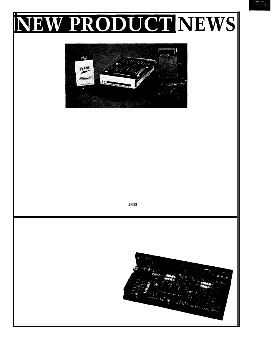
WinSystems has
introduced an alterna-
tive to the floppy disk.
The MCM-RSSD-J
Removable Solid-state
Disk Drive
is
designed
to replace conven-
tional rotating disk
memories in harsh
applications where
computers are subject
to extended temperature, magnetic fields, vibration,
dust, dirt, fumes, and so forth. The unit is totally devoid
of spindle and stepper motors, disks and bearings-
components that can fail under severe operating condi-
tions. It is designed to store programs and data for
applications such as data collection and logging, loading
program updates, diagnostics, portable instruments, and
in industrial environments where floppy disks cannot
survive.
The MCM-RSSD-J is ideal for STD bus-based
embedded systems and is compliant with the JEIDA
memory card standard. It supports the 68-pin PCMCIA
data cartridges for memory storage of up to 64 mega-
bytes. The IC memory card is small, light, and durable.
The drive will read SRAM, OTPROM, EEPROM and
flash memory cartridges, and will write SRAM and flash
memory cards.
The drive mounts directly on an STD bus card to
form a complete storage subsystem which plugs directly
into the STD bus card
cage. The drive is
equipped with panel
status LEDs which
include Low Battery
and Busy. The Low
Battery LED shows
the status of the
battery and indicates
when it needs to be
replaced. The Busy
LED indicates when
the card buffers are
enabled and that it is unsafe to insert an IC memory
cartridge.
The MCM-RSSD-J appears as an IDE interface to a
host STD bus microcomputer. An installable device
driver that supports both the DOS and ROM-DOS
operating systems is available, and the application
software then treats the MCM-RSSD as a disk drive. An
EPROM socket is on board to permit an optional BIOS
extension to enable STD bus XT- or AT-compatible
systems to boot from the MCM-RSSD-J. The MCM-
RSSD-J sells for $395.00. A CMOS STD bus version, the
LPM-RSSD-J, sells for $425.00.
WinSystems, Inc.
715 Stadium Dr., Ste. 100
l
Arlington, TX 76011-6225
(817) 274-7553 0 Fax: (817) 548-l 358
STEPPER MOTOR
and surface mount technol- MicroKinetics Corp.
DRIVER
ogy results in a very 1220-J Kennestone Cir.
l
Marietta, GA 30066
A new, high-power compact and reliable design. (404) 422-7845
l
Fax: (404) 422-7854
(lo-amp) stepper motor Overall measurements are #501
driver has been an- 6”x2.5”x1.5”.
nounced by
MicroKinetics Corpora-
tion. The DR8010
features full- and half-
stepping modes, equal-
ized torque half-stepping,
DIP-switch-selectable
current, automatic idle
current cutback, as well
as full antishorting and
thermal protection. The
use of multilayer printed
circuit board fabrication
Unique to this design is
the equalized torque half-
stepping, which smoothes
out the uneven power
difference between adjacent
steps in typical half-
stepping drives. The
DR8010 is suitable for
many CAD/CAM,
machining and manufac-
turing applications. The
DR8010 sells for
$345.00.
8 Issue
#40 November 1993 The Computer Applications Journal
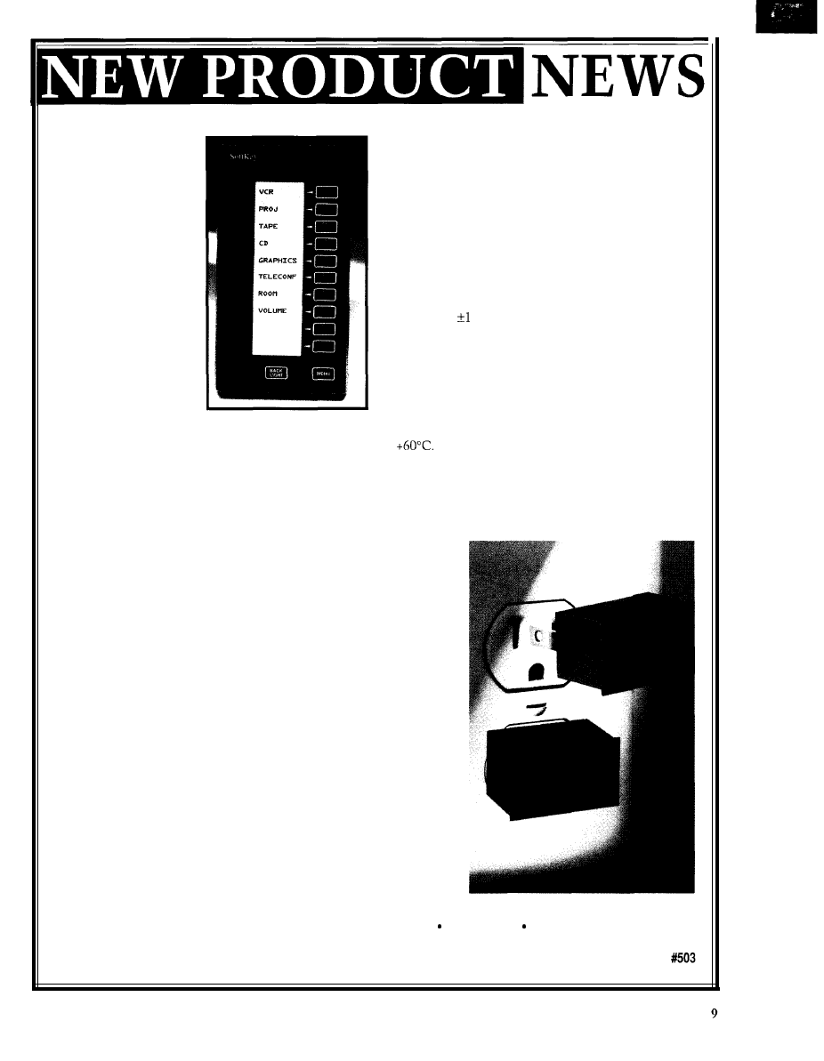
WIRELESS
PROGRAMMABLE
TRANSMITTER
capabilities and can also
The TX-SK+SoftKey
wireless transmitter from
AMX Corporation
transmit IR codes from other manufacturers. This
represents the latest
advance in program-
feature allows the SoftKey to act as a mini control
mable, menu-driven
wireless remote control.
system, directly controlling VCRs, audio components,
The SoftKey’s on-board
and video projectors.
microprocessor, multiple
control screens, and ten
function keys offer a
The hand-held SoftKey transmitter weighs approxi-
wide array of features.
mately 17 ounces and features an illuminated vertical
All transmitters
include radio frequency
(RF) and infrared (IR)
surface mount technology assure reliable trouble-free
operation. All units are overvoltage protected to 300
DIGITAL AC LINE MONITOR
DMS-20PC-l-LM is a component-sized, self-
contained, AC voltmeter for true stand-alone measure-
ments. It requires no additional components or auxiliary
power. Simply plug it into any wall outlet and instantly
read line voltages from 85 to 264 VAC (47-63 Hz). The
large (0.37”) bright-red LED display makes the unit
easily readable in virtually any lighting condition.
The DMS20PC- 1 -LM employs half-wave sinusoidal
averaging techniques (RMS calibrated) and has a sam-
pling rate of 2.5 samples per second. It features a display
resolution of VAC over the full input range of the
meter. The unit measures 1.38”xl .OO”xO.88” and is
packaged in a red filter case with integral bezel. Maxi-
mum power consumption is 0.5 W. The unit is fully
encapsulated for ruggedness. A low parts count and
liquid crystal display (LCD) that can display up to 30 text
lines.
A rechargeable NiCd battery pack is a standard
feature capable of approximately 14 hours of operation
with an S-hour charge. Low battery and charging indica-
tor messages flash across the bottom of the display
screen.
All aspects of SoftKey operation, including menus,
text, operation logic, and wireless code transmission are
programmable using AMX SKDESIGN graphical or
AXCESS software. The SoftKey has 24K of permanent
user program memory. Both compiled and source code
can be stored for most programs.
SoftKey can be programmed to provide bidirectional
RS-232 control commands via the unit’s Master/Control
port. The RS-232 port can be configured to operate as an
AXCESS Master port for program uploading and down-
loading, or as an RS-232 Control port. The TX-
SK+SoftKey suggested retail price is $1590.00.
AMX Corp.
l
11995
Forestgate Dr.
l
Dallas, TX 75243
(214) 644-3048
l
Fax: (214) 907-2053
#502
requiring
accurate AC
VAC, and the operating temperature range spans -25°C
line moni-
to
toring.
The
DMS20PC-
The DMS-20PC- 1 -LM can be used for industrial,
1 -LM AC
laboratory, office, and field service applications. Its
Line
Monitor
miniature size is perfect for design into high-end con-
sells for
$45.00 and
sumer electronics, laboratory instrumentation, and other
is available
with screw
products
terminals
for panel
mounting
and blade or
round
terminals
for socket
insertion.
Datel, Inc. 11 Cabot Blvd. Mansfield, MA 02048
(508) 339-3000
Fax: (508) 339-6356
The Computer Applications Journal Issue #40 November 1993
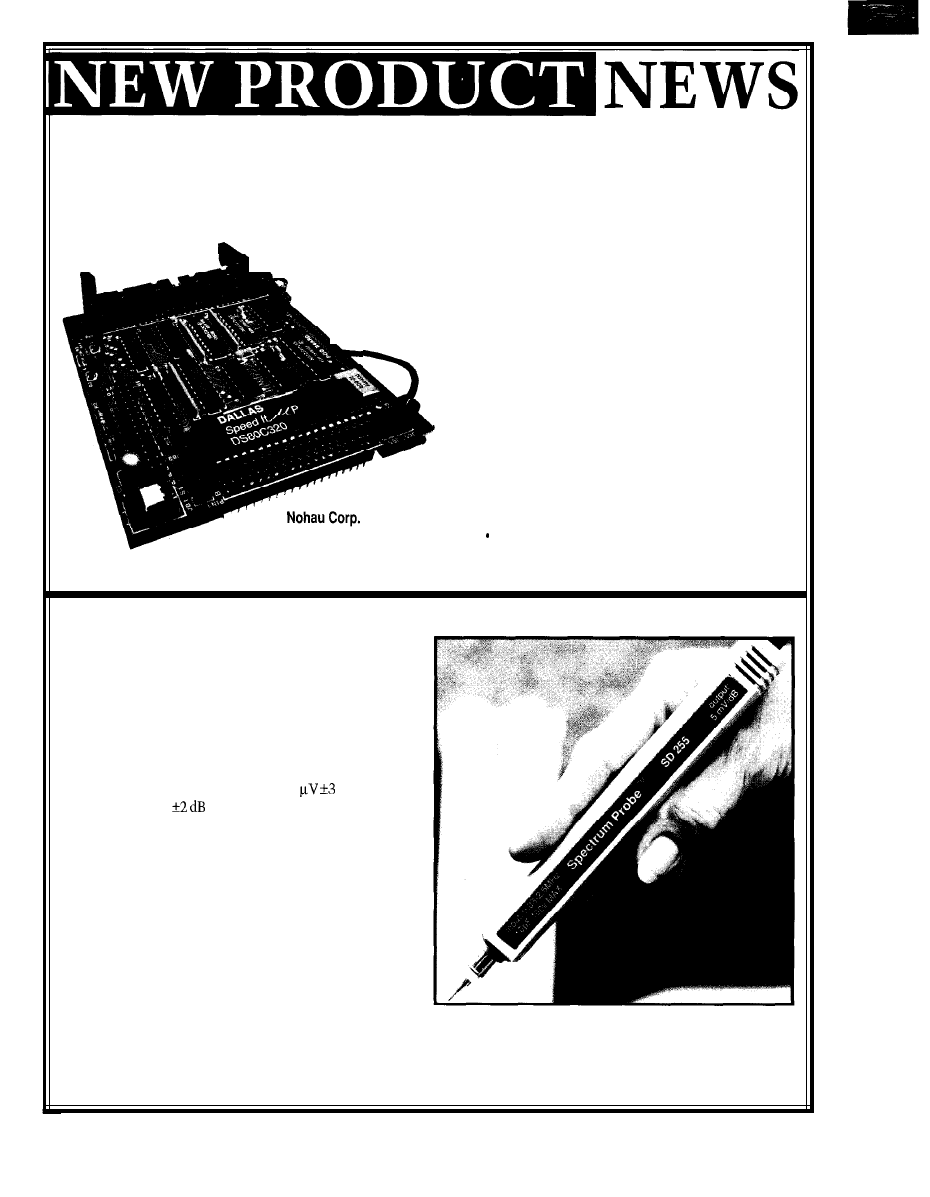
IN-CIRCUIT EMULATOR
The
EMUL5l-PC
from Nohau is a high-performance in-circuit emulator specifically designed to give an opti-
mized environment to develop 8051-family hardware and software. A special device from Dallas Semiconductor
enables Nohau to achieve emulation capabilities for the DS80C320.
The DS8OC320 is pin compatible with the 8OC32 and uses the standard 805 1 instruction set. The core is a
redesigned high-speed architecture which removes the 8051’s “dead cycles.” This
a
means that the DS80C320 will run instructions 1.5 to 3 times faster than if
they were run in a regular 8OC51 using the same clock frequency.
The EMUL5 1 -PC emulator consists of a board which plugs directly
into the IBM PC/XT/AT bus. It is also available in a box which commu-
.
nicates with the PC through a standard RS-232 channel at data
rates up to 115k bps.
.
An optional trace board holds up to 256K trace
records of 64 bits each. It has multiple trigger levels,
filtering, loop counting, on-the-fly timing, and time
stamp.
The EMUL51-PC/DS320 sells for $3595.00. The
DS80C320 probe, POD-C320 (shown), runs at speeds up to
25 MHz and sells for $995.00.
51 E. Campbell Ave.
l
Campbell, CA 95008 (408) 866-1820
l
Fax: (408) 378-7869
#504
SPECTRUM ANALYZER IN A PROBE
A low-cost scope accessory probe that can be used
for EM1 investigation is available from Smith Design.
The 255
Spectrum Probe
can be used to analyze undes-
ired signals radiated or conducted by equipment and to
view incoming signals that could cause interference.
The probe covers a frequency range from 30 kHz to
2.5 MHz and features a 60-dB [min.) dynamic range. It
features a tangential sensitivity of 40
dB at 1 MHz
with a flatness of from 0.05 to 2.5 MHz. Its input
loading is 10 pF and tip conducted radiation is nil. The
internally shielded 255 Spectrum Probe is 7.5” long, 0.9”
in diameter, and weighs only 2 oz.
The 255 Spectrum Probe can be used to measure RF
voltage or current entering or exiting electronic equip-
ment; estimate and reduce the field strength of emis-
sions; check the HF portion of infrared, ultrasonic, and
line-conducted remote controls; sniff for sources of EMI;
and indicate the source and path of RF voltages and
currents on PC boards. The conducted limits for FCC
Parts 15 and 18 and VDE 0871 fall mainly within the
range of the probe, so FCC compliance can be measured.
The 255 Spectrum Probe sells for $279. A model 107
Smith Design
Spectrum Probe is available to cover the 1 -MHz to lOO-
207 E. Prospect Ave.
l
N. Wales, PA 19454
MHz range and sells for $249 ($279 internally shielded).
Phone/fax: (215) 661-9107 #505
10
Issue #40 November 1993 The Computer Applications Journal
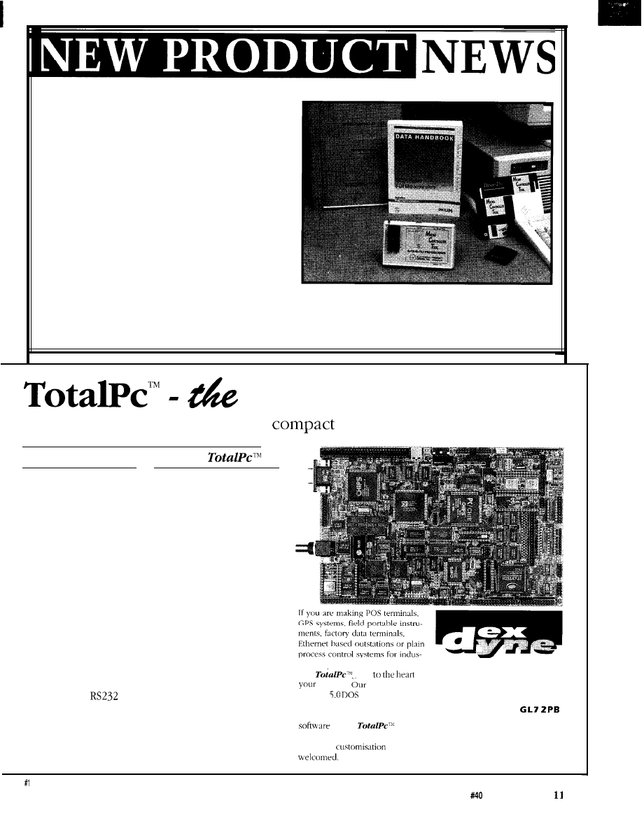
PC-BASED DEVELOPMENT SYSTEM
The MicroController Tool (MCT) is a complete,
low-cost, PC-based development system for the Signetics
87C751 and 87C752 single-chip microcontrollers. As an
optimized, integrated, and menu-driven package, MCT
includes a project manager, text editor, assembler, and
programmer. The global integration of MCT software
and features of the 87C751/752 enable the engineer and
small business to quickly develop and produce low-cost
microcontroller-based products.
The high-performance 87C751 features 64 bytes
RAM, 2K EPROM, and 19 I/O ports. The 87C752 offers
two additional I/O ports and a 5-channel, 8-bit ADC.
Both microcontrollers are derivatives of the 805 1 family
and share the same instruction set.
The MCT development system sells for $399.00 and prototyping kits are also available.
comes complete with a Microcontroller Handbook,
Operator’s Manual, software, and a Serial Programming
Electronic Product Design, Inc.
l
6963 Bluebelle Way
Module with AC adapter. MCT accessories including
Springfield, OR 97478
l
(503) 741-0778
#506
embedded system
High integration
PC controller.
l
14 MHz PC CPU with
CGA interface for
LCD/CRT display
l
Standard PC keyboard
I/F and 12 x 8 matrix
keypad interface
l
Memory space for up
to 2M byte EPROM,
4M byte of RAM and
4MBytes of FLASH
l
Watchdog timer, Time
of Day clock
l
Floppy, IDE, Printer
and 5 serial
interfaces, two with
optional isolated
RS485
l
Thin Ethernet I/F
l
VGA support for LCD
and CRT
l
PCMCIA-2 I/F with hot
insert capability
l
24 Opto 22 compatible
buffered industrial
parallel I/O lines
l
8 single or 4
differential input
12 bit ADC and 8
output 8 bit DAC
l
Fully buffered PC
Expansion slot
l
Single 5V operation.
Low power mode for
battery operation
STANDARD FEATURES OF
trial environments you will find
that
gets
of
D E X D Y N E L I M I T E D
problem.
EPROM based
Version
provides a
15
Market Place
known and proven development
Cirencester
environment for your application
Gloucestershire
on the
England
OEM and
enquiries
Tel: 0285 658122
Fax: 0285 655644
04
The Computer Applications Journal Issue
November 1993
IDE BIOS FOR EMBEDDED SYSTEMS MATH ACCELERATOR AND EMULATOR
An
Embedded BIOS IDE Development Kit
will en-
able embedded system developers to manufacture their
own IDE-compatible ROM BIOS and customize it to
meet the special needs of their embedded hardware has
been announced by General Software. Embedded BIOS
IDE comes with full source code (over 30,000 lines of
well-structured assembly language], over 112 configura-
tion options, a complete set of ROM building utilities, a
ROM disk BIOS extension module, remote disk soft-
ware, and General Software’s BIOS-aware debugger.
QuickWare has announced the release of Q387
Ver-
sion
3.5
Math Accelerator and Emulator. Q387
is a cost-
effective alternative to an 80x87 math coprocessor. The
program allows all owners of 486SX-, 486SLC-, 386DX-,
and 386SX-based PCs to run programs which normally
require a math coprocessor. Q387 is very fast, speeding
up coprocessor-optional graphics and CAD programs by
as much as 400%. Q387 is compatible with all DOS,
DOS extender, and Windows applications.
The new BIOS includes a setup screen that can be
routed to a PC screen or to a serial port using ANSI
escape sequences. Default setups are included for drive
types when no setup is possible. The primary focus of
Embedded BIOS IDE is the support of AT-compatible
BIOS functions in a real-time environment, with a low
interrupt latency of less than 10 instructions.
For laptop and notebook owners, Q387 extends
battery life by up to 25%. The program draws power
only when math operations are performed, as opposed to
a coprocessor, which drains battery power at all times.
Embedded BIOS IDE costs $1145.00. Royalties are
$1 .OO/copy, and a free product demo disk is available.
Q387 is distributed as an upgradable demo and may
be obtained free of charge by modem from CompuServe
in the IBMHW forum, America OnLine, the QuickWare
BBS at (512) 292-1212, the QuickWare Demo Line at
(512) 280-6707, or many local BBSs. Q387 registration is
$25.00 and may be accomplished toll free by phone.
General Software, Inc. P.O. Box 2571
l
Redmond, WA
98073
l
(206) 391-4285
l
Fax: (206) 557-0736
#507
QuickWare
l
P.O. Box 684652
l
Austin, TX 78658
(512) 280-1452
l
70750.2147@compuserve.com
#508
REMOTE POWER CARD!
CREATE
FILES
2 CHAN DAC
5 YEAR LIMITED WARRANTY
F R E E S H I P P I N G I N U S A
12 Issue
November 1993 The Computer Applications Journal
DUAL-BATTERY FAST CHARGE IC
The first integrated solution for fast charging one or
two nickel metal hydride (NiMH) or nickel cadmium
(NiCd) batteries is available from Benchmarq. The
CMOS
bq2005 Dual-battery Fast Charge IC
provides
comprehensive fast charge control functions with high-
speed switching power-control circuitry for one or two
independent battery-pack systems.
The bq2005 is the basis of a cost-effective solution
for sequentially charging two battery packs using flexible
control of constant-current or current-limited charging
supply. The 20-pin, 300-mil bq2005 PDIP or SOIC
package can be used as a frequency-modulated controller
operating up to 300 kHz for switched regulation of the
charging current. The bq2005 may alternatively be used
with a linear regulator or transistor to gate an external
supply.
The bq2005 supports both NiCd and NiMH batter-
ies, allowing upgrades from designs for NiCd to new
NiMH battery technology without redesign. The chip
supports charge rates of
1 to 1.5
hours for NiMH and as
fast as
10 to
20 minutes for appropriate NiCd batteries.
Fast charge begins with the application of the
charging supply or by replacement of the battery. For
safety, charge is inhibited until the battery temperature
and voltage are within configured limits. Temperature,
voltage, and time are monitored throughout fast charge.
The bq2005 includes a “top-off” charge at 12.5% of the
charge rate for NiMH batteries, as well as a user-
selectable pulsed trickle charge of
or
The bq2005 incorporates temperature slope
sensing for fast charge termination. It calculates the
slope of the battery temperature rise curve and uses the
rapid temperature increase associated with fully charged
batteries to terminate charging quickly when the rate of
temperature increase is outside predetermined accept-
able limits. In addition to
the bq2005 terminates
charge based on a sensitive negative delta voltage
detection. Fail-safe terminations include maximum
temperature, maximum charge time, and maximum
battery voltage. The bq2005 sells for $4.70 (PDIP) and
$4.80 (SOIC) in I k quantities.
Benchmarq Microelectronics, Inc.
2611 Westgrove Dr., Ste. 109
l
Carrollton, TX 75006
(214) 407-0011
l
Fax: (214) 407-9845
#509
Part5
Transceiver
C bus
256 byte RAM
Dual
stepper
50 2 A
C
quad
ADC.
DAC
controller
MT8808
HP
barcode
FCC
(full
street
phone
Firmware Furnace Embedded
pages or
Number (2
Development Board
8 parts (through
36)
72.50
5 00
8 4 0
Firmware
are
US
any pans order)
8051
(65
3
Introduction the
Set (46 pages)
8255 Cheat Sheet Reference Card
dual LED
beam)
diode controller
for
laser)
laser
controller
for
laser)
PH302
INK
Excellent
(opaque
35 mm
MC145030
LED.
8
Power op amp
supply. 3 5 A
stepper motor
8 latched 500
.
much more...
day $6 519 to 46 US slates, COD add $4 50. PO Boxes and Canadian orders $6
mail. Check, MO, COD
no credit cards.
add $50. call first NC
add 6% sales
Quantity
at
parts. Data sheets included with all parts.
Call/write/fax for seriously tempting catalog...
Pure Unobtainium
Your unusual
13109 Old Creedmoor Road
l
NC 27613
FAX/voice (919) 676-4525
2.10
2.30
2.85
Use our miniature controllers in your next product. in
your plant or in your test department. Get a wide range
of analog and digital inputs and outputs, relay and
solenoid drivers,
clocks and timers.
All our devices
provide serial communications
and
and
battery-backed
Options include
up to 40.
keypads, and expansion cards. Our easy-to-use. yet
powerful, Dynamic C development system is only
Prices start at $159, quantity one.
The Computer Applications Journal
Issue
November 1993
13
‘URES
Speed up Your M68040
with an Interleaved
Bursting EPROM
Interface
Ron
Stence
Designing with FPGAs
Loader 31: A Pseudo
EPROM Emulator
Speed upYour M68040 with
an Interleaved Bursting
EPROM Interface
EPROM memory
performance ratio for computer
systems that require high-perfor-
mance, EPROM-based program
storage. During this article, I will
explore the details of implementing an
interleaved EPROM memory for
systems based on the M68040 family
of devices and the MC68060 processor.
Since the MC68040, MC68LC040, and
MC68EC040 are each pin, bus, and
integer unit compatible, my discussion
will apply to each of these devices.
These processors will be referred to as
an M68040 integer unit or as an
M68040 processor.
In a design based on a 25MHz
M68040 integer unit, utilization of the
bursting capabilities causes a signifi-
cant improvement in performance
without more than an incremental
increase in the overall system cost.
Recently, I completed an evaluation of
various memory systems capable of
supporting the burst mode of the
M68040 processors. Currently, some
ROM manufacturers are focusing
development efforts toward creating
and marketing bursting EPROM
technology. The cost for these devices
is often prohibitive, while the memory
14 Issue #40 November 1993 The Computer Applications Journal
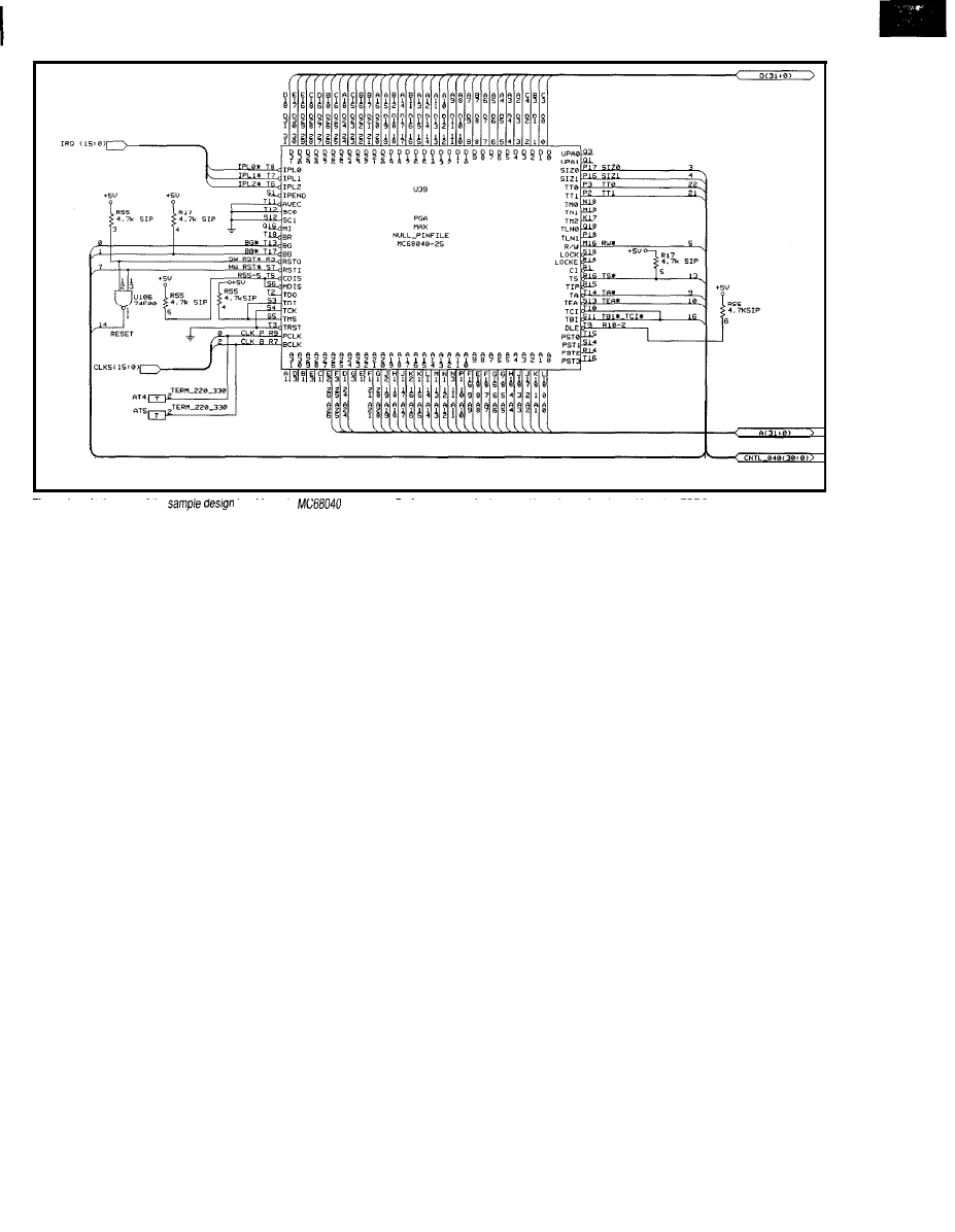
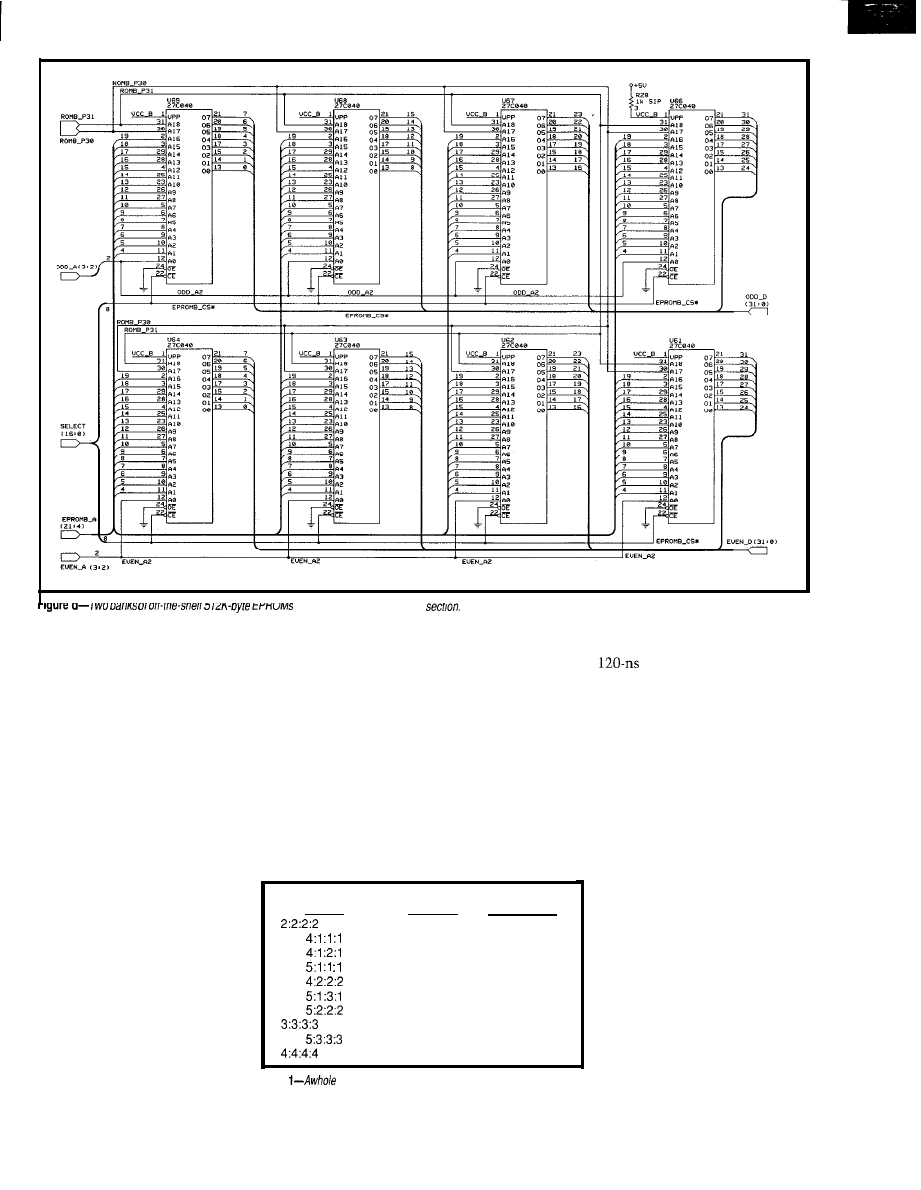
Figure la--At the core of the
IS
a Motorola
processor. Performance can be Improved by using an interleaved bursting EPROM interface.
provides a burst-enabled memory Typically, all data and instruc-
system. This system can be expanded tions benefit from bursting. However,
to create a four-way interleaved when data or instructions are highly
EPROM interface, which requires four fragmented, bursting can have a
banks of EPROMs. The more tradi-
negative effect. For example, if a
tional linear pattern uses a single bank pointer is generated to read a single
and does not allow for bursting. A value from a memory location, then
third nonbursting alternative worthy the other three accesses may never be
of consideration is to use a single used. In this situation, the unused
EPROM and an MC68 150 dynamic bus cycles can stall the integer unit while
size is limited when compared with
other EPROM devices. Costs are also
high because second sources for
bursting EPROMs are not typically
available. In this article, I will address
other methods that can be used to
create burst-enabled memory and
provide data to support the perfor-
mance improvements you may expect
from an interleaved-based design.
sizer to build the 32-bit word.
CONSIDERING THE
ALTERNATIVES
Several types of memory inter-
faces can be used to interface proces-
sors with today’s memory devices.
Most of these techniques are well
known since EPROM technology has
not changed much in the past few
years. Notable changes in this arena
have primarily focused on increasing
memory size and decreasing the access
time. Recently, several EPROM
manufacturers have begun releasing
bursting EPROMs. Designers should
be careful about specifying the current
offering of bursting EPROMs into their
products due to the lack of second
sources, limited memory size, and
higher costs of these devices.
Bursting refers to a method used
for memory accesses and also to a
microprocessor’s ability to make
multiple accesses quickly. A burst
begins with a read request to a single
address that is referred to as the initial
seed address. A memory system
capable of bursting should provide a
significant improvement in the access
time of subsequent accesses after the
initial seed has been accessed. Bursting
may not be able to provide a signifi-
cant improvement in performance if
the information, data, or instructions
are highly fragmented or if a zero-wait-
state memory system is available.
Bursting will have the greatest positive
impact when all memory references
are linear and then where the access
penalty is large for the initial access
and minimal for each subsequent burst
access.
the bus could have been used for other
required memory accesses. When a
zero-wait-state memory system is
used, the M68040 integer unit will
perform as well as, or better than,
when the bursting function is used.
BURSTING THE M68040
The M68040 integer unit has a
Harvard-style architecture that allows
the six-stage pipeline and two inte-
grated on-chip caches to operate
independently. The M68040 processor
has an integrated on-chip 4K-byte
instruction cache and a 4K-byte data
cache. Both caches are four-way-set-
associative caches composed of four
32-bit words per cache line.
Instead of using bursting
EPROMs, I have designed a two-way
interleaved EPROM system which
The relatively large instruction
and data caches can each sustain
approximately 90% hit rates. The hit
rate varies depending on the instruc-
tion and data mixes. With a bursting
The Computer Applications Journal Issue #40 November 1993 15
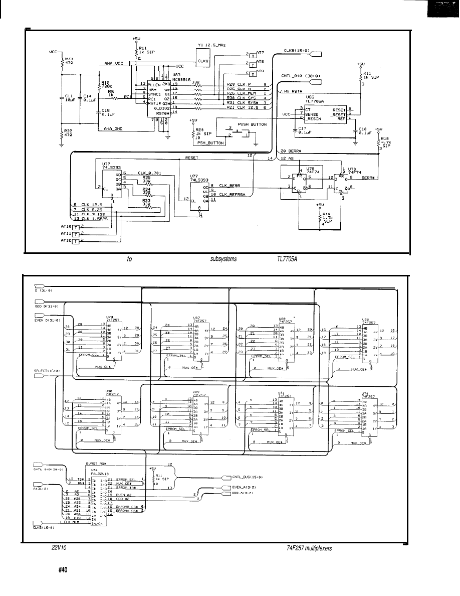
Figure 1 b--The MC88916 clock driver is used skew the main clock for the various
on fhe board. The
generates a clean reset for the board.
Figure 1 c-A
PAL implements both state machine and non-state machine signals. The state machine controls the
to switch banks of EPROMs.
16 Issue
November 1993 The Computer Applications Journal
I
rorm me core or me
memory
EPROM interface, the penalty for an the processor will supply the seed access) profile can be done by using
instruction or data cache miss is address $0000 1008. External hardware eight
EPROMs and eight
minimized. This is due to the signifi-
will be required to generate and supply multiplexers. The schematic in Figure
cant reduction in total bus traffic. the “artificial addresses” $lOOC,
1 demonstrates how to implement this
With the reduction, the instructions or $1000, and $1004. kind of memory system. No additional
data that are required to keep the The M68040 has a nonmulti-
address latches are required.
M68040 busy can be fetched from plexed address and data bus, reducing Due to the relatively high-speed
memory in a minimal amount of time. the difficulty and improving the bus on the M68040 integer unit and
The M68040 integer unit will efficiency of the interleaved design. the slow turn-off time of EPROMs, bus
access four 32-bit words for each single For example, a 25MHz bursting contention is highly possible. As a
burst sequence. The internal caches interface with a 5: 1:3: 1 (five-clock reminder, recall that bus contention
are organized to store four 32-bit words initial, one-clock second access, three-
occurs when two devices are attempt-
on a single cache line. The M68040 clock third access, and one-clock final ing to drive the bus at the same time.
integer unit will always begin
Bus contention can produce
with the access that will contain
Memory Total Number M68040
the data or instruction for which
Access of Clocks Performance
three problems: increased
the integer unit is waiting. A
bursting sequence will always
begin on a hex address ending
with any of the following values:
$0, $4, $8, or $C. Hardware is
required to increment address
No Burst
No Burst
8 clocks
7 clocks
8 clocks
8 clocks
10 clocks
9 clocks
11 clocks
12 clocks
100.0%
99.7%
97.9%
9 6 . 7 %
93.4%
92.9%
system noise, an increase in the
total system power, and system
failure when the bus drivers
blow out.
PERFORMANCE
90.1%
89.8 %
CONSIDERATIONS
bits A2 and A3 to obtain the
additional three addresses. For
No Burst
14 clocks
16 clocks
83.4%
8 0 . 2 %
The 5:1:3:1 bursting access
will yield about 93% of the
example, if hex address $0000
Table
range of bursting access
arrangements is possible.
1008 is the initial seed address,
Which you choose depends on your design.
18 Issue
#40 November 1993 The Computer Applications Journal
maximum sustained perfor-
mance available from the
M68040 Performance
0.9
Figure 2-A 2222
no burst yields the
best
performance while the performances of
ratios and numbers
of clocks off
M68040
integer unit. See Table
1
for
the memory interface derating chart. A
graphic representation of the informa-
tion contained in columns two and
three of the table is shown in Figure 2.
Three points should be considered
in making the entire burst access as
efficient as possible. The most impor-
tant part of the bursting sequence is
the first access. Insertion of an addi-
tional clock cycle will typically incur a
3% degradation in performance.
The next most critical point is the
second access. Often the M68040
M86040 Address Even Bank Odd Bank Multiplexer
0 0 0 0 Even Bank
1 1 Odd Bank
0 0 Even Bank
1 1 Odd Bank
0 1 1 0 Odd Bank
0 1 Even Bank
1 0 Odd Bank
0 1 Even Bank
1 0
1 1
integer unit will be starving for the
first access. Once that has been
accomplished, the M68040 integer
unit will typically accept the second
access into the first stages of the
instruction pipe. When the second
access is delayed by too many clocks, a
bubble
can occur in the instruction
pipe. This will degrade the possible
performance of the machine.
The third point to be considered is
the total number of clocks for the
complete burst transfer. The third and
fourth transfers can degrade the
possible performance by
one or two percent for
every additional clock
cycle that is added.
Typically, this is caused
by stalls in data or
nonsequential instruc-
tion fetches or data
writes that have filled
the write-back buffer.
The M68040 integer
unit is less susceptible
to memory degradation
than many other
processors available
today. This is due to
three factors: the
M68000 processors have
a relatively high code
1 1 Odd Bank
0 0 Even Bank
1 1 Odd Bank
0 0 Even Bank
0 1 Even Bank
1 0 Odd Bank
0 1 Even Bank
1 0 Odd Bank
Table
interleaved EPROM interface accesses two banks of
density;
code is
memory: an even bank and an odd bank. Depending on address bit A3 from
typically half the size of
processor, the interface access the even or odd bank first, followed
a
RISC processor; and a
by the
opposite bank.
RISC processor is a
TO
AR-16
INTERFACE . . . . . . . . . . . . . . . . . . . . . . . .
99.95
Two 8 channel relay output ports are
for control
up 16
to 128
ays
expansion
Each
output port connects a
relay card or terminal
A variety of relay cards and
for more info.
to
feet).
be used
AR-1 6 interfaces.
(up
lo 16.
REED
EX-16 RELAY
D I G I T A L
To
(terminal
and
sold separately)
ST-32 STATUS EXPANSION
79.96
on/off status of relays.
thermostats, security devices. smoke detectors and
devices including keypads and binary coded outputs.
32 statue inputs
isolators sold separately).
TE% TEMPERATURE INPUT CONVERSION . .
$49.66
temperature sensors 8 terminal block.
Temperature ran e minus
145
F.
PORT
(4
RS-422) . . .
converts an
4
AS-422
TOUCH TONE
end
interfacing
available.
for free information packet.
FULL TECHNICAL SUPPORT..
over the
telephone by our staff. EACH ORDER INCLUDES A
FREE DI
S
K
EXAMPLES
I N
BASIC, C AND ASSEMBLY LANGUAGE.
reference manual is also included.
for continuous 24
hour industrial applications.
socketed.
. Use
IBM
Tandy. A
other
with RS-232 or
All standard baud rates and protocols may be
used
19,200 baud).
Use our
number
order FREE INFORMATION
PACKET. Technical
(614)
24 HOUR ORDER
Visa-Mastercard-American Express-COD
International Domestic FAX (614)
Use for information,
support orders
ELECTRONIC ENERGY
INC.
South
Street,
604
43215
The Computer
Journal Issue
November 1993 19
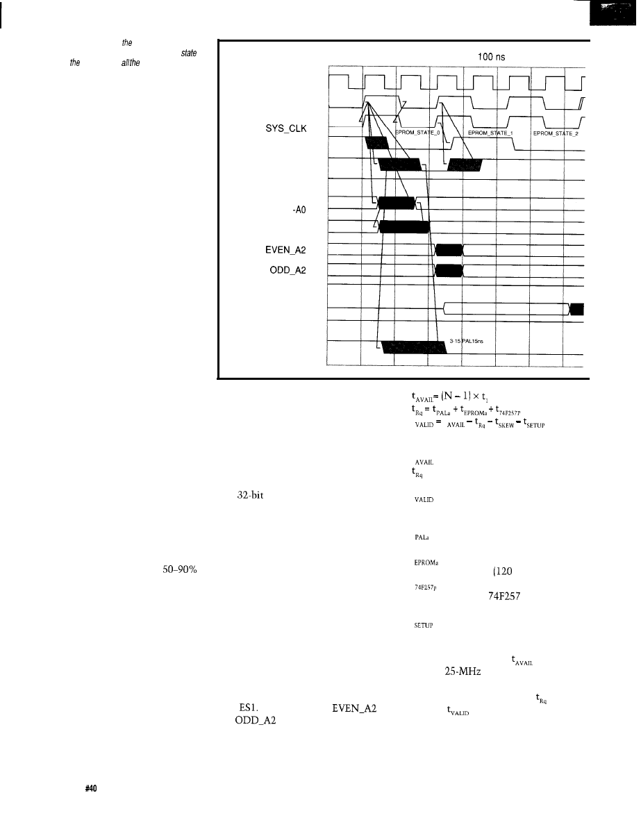
Figure
3-Precise timing of interleaved EPROM
interface is critical for successful operation. The
machine in PAL handles tricky timing
sequences.
store based architecture, which does
not have the ability to modify memory
directly.
On a RISC processor, all instruc-
tions are a fixed length, resulting in
wasted bits in the instruction fields.
M68000 instructions can be 16 bits or
larger, depending on the addressing
mode or immediate data fields that are
included in the instruction. This
results in very dense instruction
fetches and more efficient utilization
of the instruction cache. The second
factor is the relatively large instruction
and data caches integrated on-chip.
The third factor is the bursting
interface coupled to the six-stage
integer instruction pipe.
When a burst is initiated, a
potential data write is delayed while
the instruction(s) are fetched. Because
data writes can be delayed, the
M68040 can fetch instructions or data
that are needed to keep the instruction
pipeline full. The M68040 integer unit
requests the required instruction first
and bursts in the remaining three
fetches. Typically, the M68040 integer
unit will need the next instruction
within one to four clocks after fetching
the first instruction.
After bursting, the M68040 integer
unit has four or more clock cycles
when the integer unit will not require
the data bus for instruction fetches.
This allows the processor to update
memory or fetch new data. The
M68040 integer unit will use
of the total available bus bandwidth.
The lower bus utilization allows other
devices such as DRAM refresh, DMA,
or slow peripherals to take advantage
of the available bandwidth without
impacting performance.
The interleaved EPROM interface
accesses two banks of memory-an
even bank and an odd bank. Depending
on address bit A3 from the M68040
processor, the interleaved EPROM
interface will access the even or odd
bank first, followed by the opposite
bank. See Table 2 for the incremental
burst-sequence decode. The interleave
PCLK
BCLK
STATE-MACHINE
TS*
TA*
A31
BUFFER_ADDR
MUX-DIR
EPROM-DATA
MUX_OE*
EPROM_CS*
0
ns
20ns
40ns 60ns 80ns
1 2 0 n s 1 4 0 n s
control PAL decodes the state of the
M68040 integer unit’s address bits A3
and A2 to decode which bank of
memory (the even or odd bank]
should be selected for the M68040
integer unit’s data bus. During a
bursting sequence, both banks of
memory are each accessed twice. The
four
words fill a cache line. The
interleaved control PAL increments
the even A2 and the odd A2 signals to
provide the two accesses with different
addresses for each EPROM bank. The
computation of the timing required for
the interleaved EPROM memory
system is greatly simplified by the
synchronous bus on the M68040
integer unit.
TIMING CONSIDERATIONS
The first access begins at the
rising edge of the BCLK. The signal
TS* is asserted for 10 ns or more. This
condition causes the state machine in
the interleaved control PAL to go to
state
Assertion of the
and
to the correct logic
levels occurs between 2 ns and 15 ns
after the rising edge of the BCLK when
a 15 ns PAL is used.
t
t
where:
t
= total time available
= time required by interface logic
and memory
t
= time available remaining
N = number of clock cycles
t, = time period of the bus clock
t
= PAL logic access time to
valid outputs (15 ns)
t
=
EPROM access time to
data valid
ns)
t
= maximum propagation
delay for
(7 ns)
tSKEW = maximum clock skew
t
= maximum setup time on
M68040 (5 ns)
Computation of equation
is 160
ns when a
M68040 integer
unit with a five-clock initial access is
used. Computation of equation is
142 ns and
is 18 ns (specification
16 of the M68040).
The hold time
requires that data be held valid for a
minimum of 4 ns after the rising edge
of BCLK.
2 0
Issue
November 1993
The Computer Applications Journal
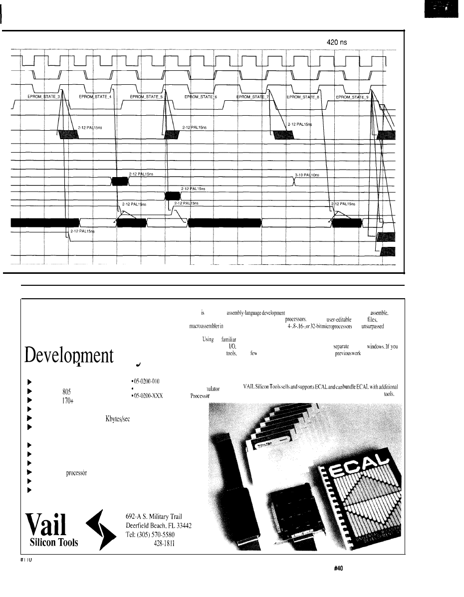
160ns 180ns 200ns 220ns 240ns 260ns 280ns 300ns 320ns 340ns 360ns 380ns 400ns
440ns 460ns
ECAL Universal
Assembly Language
Product Information
Svstem
ECAL a complete
system that provides all the tools needed to
Imk,
load. run, and debug your project for over 170
By using
control
the ECAL
its full configuration can handle
with
speed
and consistency.
the
DOS-bated text windows. you can edit, assemble. set breakpoint,. trace execution,
watch registers and
and communicate with your target’s serial port in
closable
prefer to use other
with a
keystrokes. ECAL will incorporate your
into its consistent
and intuitive environment.
Ordering Information
Alternative to Real-Time Emulator
ECAL OAS
Support for
1.8096, and 186
05-0200-020 ECAL with EPROM En
Support for
additional processors
ECAL Single
User control of syntax and instructions
Extremely fast assembly--?
Integrated split-screen editor or command-line
assembly supported
Integrated linker/loader
Instruction trace and I/O windows
Monitor and RS-232 corn. windows
Single micro
versions available
Optional EPROM emulator and programmer
Source-level debugger
Contact
Vail Silicon Tools
The free ECAL evaluation program features all of the ECAL tools for all ot the
supported micros. giving you a true sampling of ECAL development cycle (source and
object length limited).
hardware and software to satisfy your need for economical project development
Fax: (305)
The Computer Applications Journal
Issue
November 1993
2 1
HOLD =
t
+
+
where:
t
= PAL logic minimum propaga-
tion time (2 ns)
t
= EPROM hold time (0.0 ns)
t
= minimum propagation
delay for
(2 ns)
Calculation of equation
is 0.0
ns for all four accesses. Refer to the
hold time timing diagram, shown in
Figure 3 for additional information.
The 0.0 ns of margin on the hold time
does not cause a problem when the
following considerations are taken into
account.
First, the EPROM manufacturers
specify 0.0 ns hold time from chip
select negation to data invalid. This is
not very realistic and some EPROM
vendors are beginning to specify 4 ns
(or more) hold time. Second, the clock
driver should be placed near the
M68040 integer unit to reduce trans-
mission line effects and
noise.
This results in the BCLK trace to the
M68040 integer unit being signifi-
cantly shorter than the trace to the
interleaved control PAL which adds to
the total data hold time.
The clock driver chosen can make
a significant difference in the clock
skew time. When using a MC889 15 or
MC88916 clock driver, the output
chosen can further reduce the skew
between the BCLK and the clock pin of
the interleaved control PAL. For
example, the MC88915 clock driver’s
Q4 clocks 34
or more (up
to 275 ps) before QO. When the Q4
output from the MC88915 is used to
drive the M68040 BCLK pin and the
QO is used to drive the interleaved
control PAL, the BCLK will always
lead the PAL logic output. When using
the MC88915 to drive the system
clock, the clock skew becomes 0.034
ns positive. If the
integer unit
cannot be used with the MC88915 or
MC88916 in this configuration, a delay
can be introduced into the interleaved
control PAL clock. A typical delay
device might be a
where the
low-to-high specification is 3.0 ns
minimum and 6.6 ns maximum. The
interleaved control PAL clock should
not exceed an
delay because the
Figure
EPROM
Machine
Diagram
interleaved control PAL could miss the
TS
l
signal from the M68040 integer
unit.
Finally, the trace length and
capacitance of the control signals and
data bus need to be at a minimum to
require any calculations to be per-
formed on the trace or wire delay.
Furthermore, the trace and device
capacitance contribute to the total
hold time. The hold time of 0.0 ns
should not be a problem when a
resolution clock driver is used. The
maximum clock skew should never
exceed 1 ns or BCLK will lead the
interleaved control PAL clock.
The second access has one
additional clock period to access the
EPROM. The second access setup time
(t.
is 240 ns and the
is 63 ns.
An additional quick check should be
performed on
when the multi-
plexer is changed from one input to
the other. The minimum multiplexer
select time is 3 ns. The interleaved
control PAL clock-to-state change is 2
ns. When using the MC88915 or
MC88915 clock driver described
above, the clock skew is negligible and
the
time is 1 ns.
The third access has timing that is
similar to the first and second ac-
cesses. The for the third access is
142 ns, so
is 18 ns. A similar
argument can be made for the fourth
and final access.
THE PROCESSOR’S PAL
The PAL equations to control the
interleaved EPROM interface fit into a
single 22VIO device. The code used to
program this device is shown in
Listing 1. The inputs to the PAL are a
system clock, TS*, R/W*, and
address signals from the M68040
processor. The last input is a combina-
tion of several signals to create the
BURSTRQ’ signal. The BURSTRQ
l
signal is asserted low when the
M68040 processor attempts to burst,
indicated by the assertion of SIZE1
and SIZE0 signals to a high logic level.
can be derived inside the
with an equation, or a
can be used to conserve input pins.
The outputs of the interleaved
EPROM PAL are in two groups. The
first group is the non-state machine
outputs and the second group contains
the state machine outputs. The signals
in the non-state machine group are the
EPROM chip select (EPROM_CS*) and
the even and odd address bit 2
and
The signal
* will assert when the
address is valid and the TS* signal is
asserted. The
signal
remains asserted until the state
machine returns to the
or the
starting state. The chip select signal
will assert only during a read opera-
tion. A write causes the EPROM_CS’
signal to negate and the state machine
to go to ESO.
The
and
signals begin the toggling process
based on the original value of the A3
and A2 address bits from the M68040
processor. For this discussion, an
address will be considered “even”
when the address from the M68040
processor decodes to the even bank
first. An “odd” address will decode to
the odd bank first. All first accesses
beginning with a $0 or $C will begin
with the even bank. All first accesses
beginning with a $4 or $8 will begin in
the odd bank of EPROM. For example,
the address $0000 0004 causes the first
access to occur in the odd bank. If the
first access were memory location
$0000 OOOC, the access would be even.
2 2
Issue
November 1993
The Computer Applications Journal
Listing l--The
handles both state machine and non-state machine signals. contains fhe main
logic for interface.
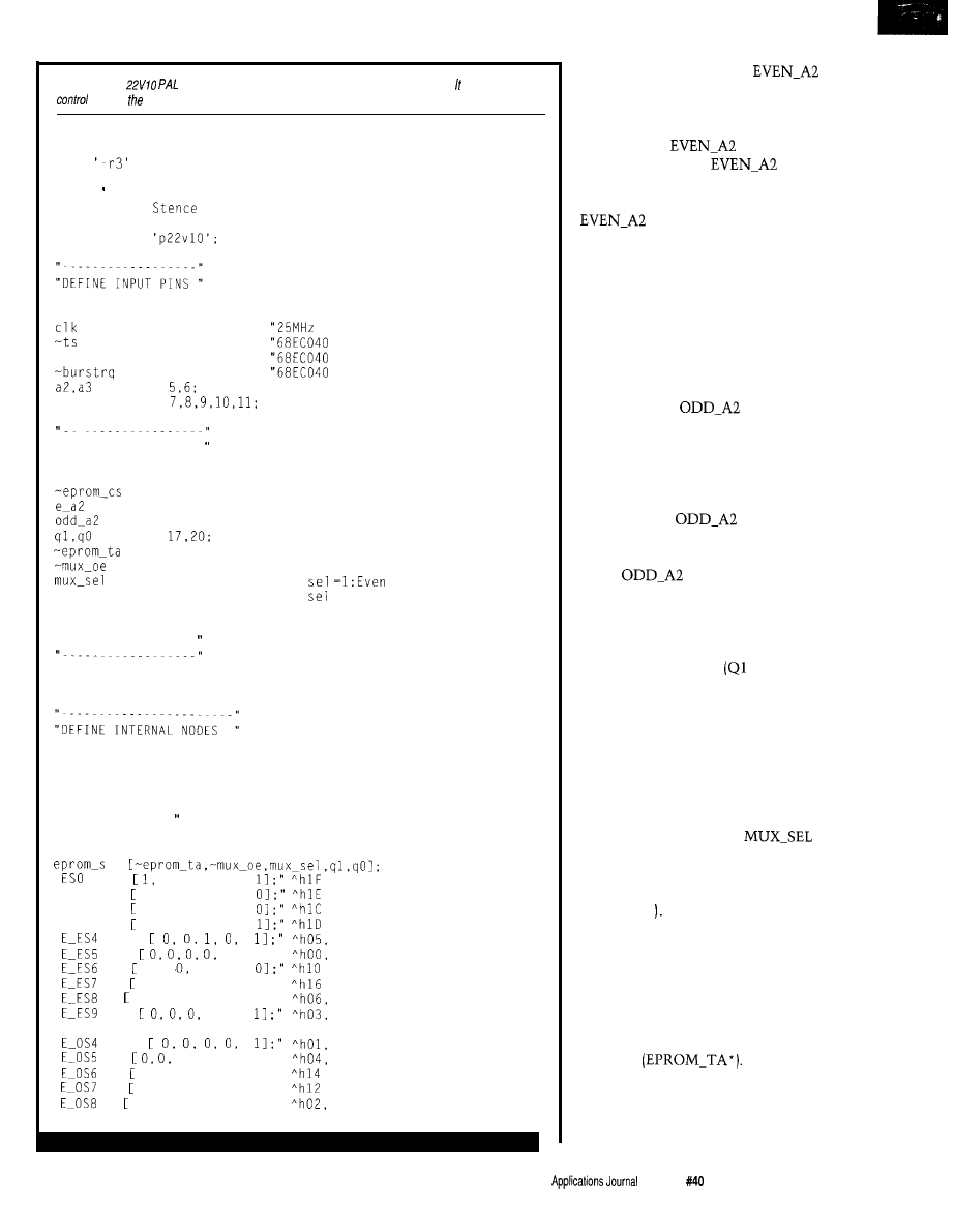
MODULE INTERLEAVED-EPROM:
flag
TITLE Interleaved EPROM PAL Eq.
Ron
Motorola Inc.'
inter device
pin 1;
system clock
pin 2:
transfer start
read pin 3;
read-write
pin 4;
wants to burst
pin
"address bus
Address pin
"address bus
"DEFINE OUTPUT PINS
pin 16; "EPROM Chip Select
pin 19; "even EPROM A2
pin 18; "odd EPROM A2
pin
"state machine outputs
pin 21: "EPROM Transfer Acknowledge
pin 22; "EPROM data MUX output enable
pin 23; "mux
EPROM
"mux
=O:Odd EPROM
"DEFINE CONSTANTS
X,C,Z,K =.X.,.C.,.Z.,.K.:
RESET node 25: "A Write to EPROM will Reset this state machine!
"DEFINE VECTORS
=
=
1, 1, 1,
ES1 = 1, 1, 1, 1,
ES2 = 1, 1. 1, 0,
ES3 = 1, 1, 1, 0,
=
assert TA to even EPROM
=
01:"
assert TA to odd EPROM
= 1, 0, 0,
= 1, 0, 1, 1, 01;"
= 0, 0, 1, 1, 01;"
assert TA to even EPROM
=
1,
assert TA to odd EPROM
=
assert TA to odd EPROM
=
1, 0, 01;"
assert TA to even EPROM
= 1, 0, 1, 0, 01;"
= 1, 0, 0, 1, 01;"
= 0, 0, 0, 1, 01;"
assert TA to odd EPROM
(continued)
The PAL equation for
begins with the signal asserted to a
low logic level when the address is
“even.” The basis of the PAL equation
for the signal
is an exclu-
sive-OR. The signal
is used
for the first and third accesses when
the address is “even.” Therefore,
will be toggled immediately
following the first access to allow the
even EPROM bank to begin the next
access. Once the third access has been
terminated, the signal EVEN-A2
becomes a “don’t care.” When an
“odd” access is initiated, the signal
EVEN_A2 will begin with a high logic
level and the toggling will begin at the
end of the second access.
The signal
follows the
initial value of the signal A3 from the
M68040 processor for both “even” and
“odd” addresses. When the address is
“odd,” the first access will be to the
odd bank. At the end of the first and
third accesses,
will toggle.
When the address is “even,” the first
access will be to the even bank and the
signal
will toggle at the end
of the second access.
The EPROM state machine is
composed of five bits. Two bits were
used to create unique or distinctive
state machine outputs
and QO) so
a Grey code type of count could be
used. However, not all state changes
are true Grey code. This does not
cause a problem since all signals using
the state machine outputs are regis-
tered. The next bit is the multiplexer
select bit (MUX_SEL). When this bit is
a logic high, the multiplexer selects
the even bank. When the
bit is a logic low, the multiplexer
selects the odd bank. The fourth bit is
the multiplexer output enable bit
(MUX_OE* When this bit is asserted
to a logic low, the multiplexer drives
the data bus of the M68040 processor.
When the MUX_OE* bit is negated to
a logic high, the multiplexer becomes
a high-impedance output. The final
output of the EPROM state machine is
the acknowledge signal to the M68040
processor
The output pin EPROM_TA’ uses
an open-collector-type output. This
will reduce the number of inputs to
the acknowledge PAL equation and
The Computer
Issue
November 1993 2 3
allows other devices to be connected
together to drive EPROM_TA* to a
low logic level. Other signals that can
be connected to the EPROM_TA*
signal net are the acknowledge from
the interrupt PAL or from other
peripherals PALs. A pull-up resistor is
required when this configuration is
used.
STATE MACHINE CAVEATS
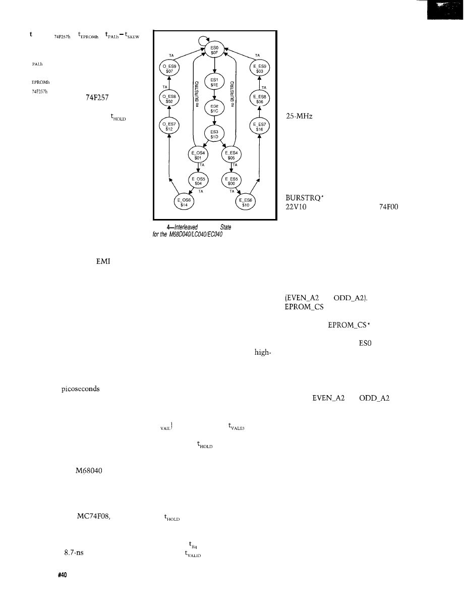
The state machine (refer to Figure
4) can be modified easily to increase or
decrease the number of wait states. To
increase the number of wait states, an
additional state should be added before
states ES3, E_ES7, and E_OS7. To
decrease the number of wait states,
remove states ES3, E_ES7, and E_OS7.
When changing the state machine,
two points must be considered. The
Grey code may need modification to
minimize state changes. The
Ql
and
QO outputs can be modified to mini-
mize the number of state changes
without impacting the operation of the
PAL equation. Second, the state
machine is running ahead of the
M68040 processor. For example, the
EPROM_TA’ is asserted during state
E_ES4. However, the M68040 proces-
sor will actually accept the data and
TA* signal on the rising edge of the
BCLK. The state machine will exit the
E-ES4 state at the same time. There-
fore, the modification to the state
machine should take place when the
state machine is going through wait
states.
USING THIS NEW TOOL
Several types of applications are
well suited to an interleaved-EPROM-
based design, such as laptop comput-
ers, low-power computers, embedded
controllers, and laser printers. A laser-
printer-based application can benefit
greatly from an interleaved EPROM
interface due to the cost sensitivity of
the laser printer market while being
driven to provide higher performance
for the same system cost. Laser
printers typically will not copy
instructions and fonts into DRAM.
The interleaved EPROM interface will
provide DRAM equivalent perfor-
mance without a significant increase
in the cost of the system.
Listing
1-confinued
= 0, 0, 1, 1, 11;"
assert TA to even EPROM
addr = [Address];
state-diagram
state ESO:
if
== Address)) then
else ESO:
state
state
E3;
state ES3:
if
then
else
state
"Assert TA, MUX
= 1
if
then
else ESO; "no burst
state
"Assert TA, MUX
= 0
state
state
"Assert TA, MUX
= 1
state
"Assert TA, MUX
= 0
state
ESO;
state
"Assert TA, MUX
= 0
if
then
else ESO: "no burst
state
"Assert TA, MUX
= 1
got0
state
state
"Assert TA, MUX
= 0
state
"Assert TA, MUX
= 1
state
ESO;
equations
RESET =
:=
==
==
==
==
==
==
==
==
==
==
==
==
==
==
==
:=
==
==
(a3
==
==
==
==
==
==
(continued)
24 Issue
November 1993
The Computer Applications Journal
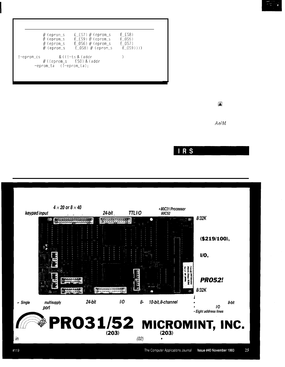
Listing
l-continued
==
==
==
==
==
==
==
==
= read
== Address)
!=
== Address)));
enable
=
end INTERLEAVED-EPROM;
The interleaved EPROM interface
has several positive points to be
considered. The most significant is a
dramatic increase in system perfor-
mance while reducing bus utilization
and memory latency on the M68040
integer unit. Second, the total system
power can be reduced when the
EPROMs do not have to be copied to a
higher-speed memory system. When
the EPROMs are not copied, power and
money can be saved while not support-
ing a second memory system. Third,
there will be a reduction of bus
contention between the EPROMs and
the M68040 integer unit. Finally,
when data bus buffers are required, the
change to multiplexers will have little
or no effect to the cost of the system.
An interleaved EPROM interface
does have several negative attributes
which should be considered before
using it in a design. First, there is an
increased number of EPROMs in-
cluded in the design. This technique
should not be considered when the
design will be using eight or more
EPROMs. Second, there is an increased
number of support devices such as
multiplexers. Third, the increased
complexity in the control logic could
result in an increase in the board size.
Finally, the potential increase in total
system cost should be considered.
The change to an interleaved
EPROM interface can be done with a
small increase in complexity and
system logic. The positive and nega-
tive attributes, such as total system
size, cost, and performance levels,
should be considered before changing
to an interleaved interface. A require-
ment to make a dramatic improve-
ment in the system performance could
make an interleaved-EPROM-based
design a wise solution.
Ron Stence holds a B.S. in Computer
Science from the Department of
Engineering at Texas
Univer-
sity. He is currently a senior systems
applications designer in Motorola’s
68000 marketing applications group.
401 Very Useful
402 Moderately Useful
403 Not Useful
PRO = Positively Rampant Optimization
CMOS
PROCESSORS
Hardware real-time clock
or
4 x 5
LCD display output
parallel
l
with BASIC52
Power inputs Auxiliary serial port
parallel TTL
&bit, I-channel
DAC
supply
or
option
or
A DC
Console serial
Hardware watchdog
RAM
PRO31 prices start
a5 low as $289
includes SK RAM,
watchdog, 56 bits
S-bit ADC,
and LCD interface.
And it only costs
$10 more for
ROM
EXPANSION HEADER
Port 1 processor
lines:
77L
Six decoded
address strobes
4 Park Street
l
Vernon, CT 06066
l
871-6170
l
Fax
872-2204
Europe: (44) 0285-658122
l
in Canada: (514) 336-9426
l
in Australia:
888-6401 Distributor Inquiries Welcome!
Designing
with FPGAs
Del Hatch
Part 1: An
Overview
0
here is no doubt
about it-today’s
electronic designs are
more complex and
contain more logic than ever before.
We all like to see lots of bells and
whistles in electronic products (even
those we design) and this requires
more and more logic to do the job.
However, this complexity causes a
variety of problems. Having lots of
chips in a design is expensive, and not
simply the cost of the parts. They
require a lot of board space and a lot of
traces on a printed circuit board to
interconnect them all [or sore wrists
and fingers if you wire-wrap your
designs). A board with a lot of logic
chips is almost always current-hungry
as well.
One solution to these problems is
to put more and more logic onto each
chip. Where only a little bit of logic is
required, programmable array logic
(PAL) chips can be used. The amount
of standard parts that can be replaced
by a typical PAL varies by size of the
PAL and the type of circuitry you’re
trying to replace, but for most cases
you can count on replacing around ten
TTL chips with one medium-sized
PAL. These programmable chips have
proven very useful because they are
inexpensive and can be programmed in
the lab or at home.
MY LOGIC GROWS AND GROWS
But what do you do if you have
more logic than can fit into a single
PAL? Of course! You use more PALs,
right? Not if you know how to use the
latest in digital integrated circuit
technology. The proper solution for
many designs is applying a field
programmable gate array (FPGA)
instead of a handful of PALs. “Field
programmable” means they can be
configured in a lab or home workshop
to perform custom functions.
This relatively new family of
chips is produced by a few different
companies, and can put the equivalent
of hundreds of gates into a single,
inexpensive chip. They are great for
prototyping designs that will eventu-
ally be made in large quantities, as
well as a “production run” of a single
breadboard.
Many engineers, as well as people
who like doing custom designs at
home, may feel these chips are too
exotic, or too hard to program, or too
expensive to use in designs, but
I
have
found the opposite to be true. When a
moderate-to-large amount of logic
needs to come together, FPGAs are a
quick, easy, almost fun solution. The
fun comes from seeing a design that
incorporates a lot of logic run in a
single chip on your board.
With the eventual goal of showing
you how to make something useful
with these chips, it is best to look at
them in more depth. To do this, I will
start by looking at the principles
behind programmable logic devices,
and then how some manufacturers use
these concepts in FPGAs. Then I will
look at other styles of FPGAs that
broke from the PAL mold and use
small “chunks” of logic that are
connected together to form a design.
In the article that will appear in
next month’s issue, I will show you
how to take a design from concept to
finished product, with a unique desk
clock as an example. But, this month
I’ll concentrate on the facts of the
matter.
PROGRAMMABILITY
Each of these families of products
falls under the more general classifica-
tion of a Programmable Logic Device,
or PLD for short. PLDs contain logic
gates just like any other digital chip,
but this logic is arranged differently.
Instead of prewired, fixed paths for
interconnecting the logic, PLDs use
programmable links to connect gates
together. In most PLDs, it is not the
logic inside the devices that is changed
26
Issue #40 November 1993 The Computer Applications Journal
INPUT
INPUT
Figure
of a
PAL shows the programmable connection matrix and the AND/OR logic structure.
two inputs A and B can be written two
w a y s :
inverted form. Each of the AND gates
(which are drawn just to the right of
the wiring array) is shown with only
one input, but this is only to simplify
the diagram. In reality, each AND gate
can operate on any of the signals that
run down the vertical tracks.
The OR gates that follow the
OUTPUT
AND gates do just what they look
like-they OR together each of the
seven signals coming from the AND
gates. In this way, logic equations can
be implemented directly from the
sum-of-products form.
For example, the XOR function of
during programming-just the inter-
connections.
will later see that
some
broke from this mold by
storing more than just interconnection
information.
The earliest and still very popular
method of programming an intercon-
nection was to blow a fuse-like
connection open, so that unwanted
connections are not made. When the
PLD is manufactured, all interconnec-
tions on the chip are already made, and
the user opens up those connections
that are not wanted.
There is another method of
determining how connections are
made. Some
use an
which is the opposite of a fuse, as the
name implies. A connection location
is manufactured in a high-resistance
state (as opposed to the low resistance
which an unblown fuse provides) and
the user can then program it to
become a low-resistance connection.
In other words, no connections are
premade during manufacturing.
Instead, the user creates “shorts” that
make the desired connections to
implement the proper logic functions.
Another kind of PLD technology
is similar to that
in EPROMs.
These
are based on EPROM
technology so the connection informa-
tion can be erased with ultraviolet
light. This allows the device to be
reprogrammed should the design
change. With fuse- or antifuse-based
a mistake causes the entire PLD
to become scrap. EPROM-based
can be used over and over.
Another connection technology
uses CMOS transistors in a pass-gate
configuration. The signals pass
through the connection depending on
the logic level applied to the gates of
the transistors. This logic level is not
stored permanently in the FPGA, but
instead read into the device every time
power is first applied. This also means
the FPGA itself is not programmed and
thus another external storage device is
needed.
PAL BASICS
The basic operation of a typical
PAL is easy to understand. Referring to
Figure
1,
input signals enter the
diagram from the left and are sent out
on the vertical rails in their true and
or as,
Y = AB’ A’B
The second form shows how the
output term is generated in a PAL-like
device. One AND gate will have two
inputs: the A signal and the inverted B
signal. These signals are available on
the vertical wiring paths as described
before. The second AND gate similarly
connects the inverted A input and the
noninverted B input. The OR gate that
follows the AND gates then takes
those two terms and generates the
final output Y.
The PAL quickly became the
standard for programmable logic due to
the simplicity and parts count
To
Block
Product Terms Clock Clear
ure
has a PAL-like structure of AND/OR gates but is more
me
be cleared and clocked from global or
generated signals.
The Computer Applications Journal Issue
November 1993 2 7
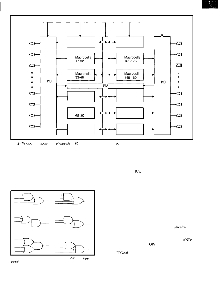
Controls
and
Clock
M a c r o c e l l s
Macrocells
l
1-16 177-l 92
Control
Block
M a c r o c e l l s
Macrocells
49-64 129-l 44
l
M a c r o c e l l s
Macrocells
113-128
Control
Block
M a c r o c e l l s
Macrocells
81-96 97-l 12
Figure
FPGAs
groups
and blocks which communicate through
P/A wiring resources.
tions that were possible. Another
necessary part of their success was due
to the software tools. It would be
tedious for a human to figure out all
the fuses that need to be blown, and so
PAL manufacturers developed pro-
grams that would automatically create
the necessary files. Without automated
software tools, all programmable
devices are virtually useless. A user
relies so heavily on software that the
tools available can often determine
which device to use.
For a long time, a PAL user
usually had very few options when it
came to entering the design into these
software tools. It usually required the
logic equations to be entered. The
program would then
generate a fuse map
that contained the
information on
which fuses to blow,
and then a special
programmer would
modify (program) the
chip with the proper
connections.
more logic to be incorporated into one
chip, thus requiring less space on a
circuit board. For most people, one of
the most painful things about
prototyping is wiring together all the
With an FPGA, the logic can often
be reduced to a small number of chips.
FPGAs also allow for rapid
changes in a design. Instead of rewiring
a lot of logic, changes are simply made
by programming another FPGA (or in
the case of reprogrammable devices,
simply reprogramming the same
device). This reduces the stress of
having to get it perfect the first time
and reduces the cost when you don’t.
It also makes it more desirable to add
functionality later because it is so
painless to add logic to an
completed design.
Figure 4-These
are a few typical multiple-gate functions
can be
in a sing/e ACT 1 logic module.
ENTER THE FPGA
Like their PAL predecessors, some
A major revolu- FPGAs use a wiring matrix that
tion began when and then
the input signals. The
field programmable most popular manufacturer of this
gate arrays
type of FPGA is Altera. (The term
were introduced. “manufacturer” is not entirely
FPGAs allow for a lot accurate. Like most FPGA companies,
28
Issue #40 November 1993 The Computer Applications Journal
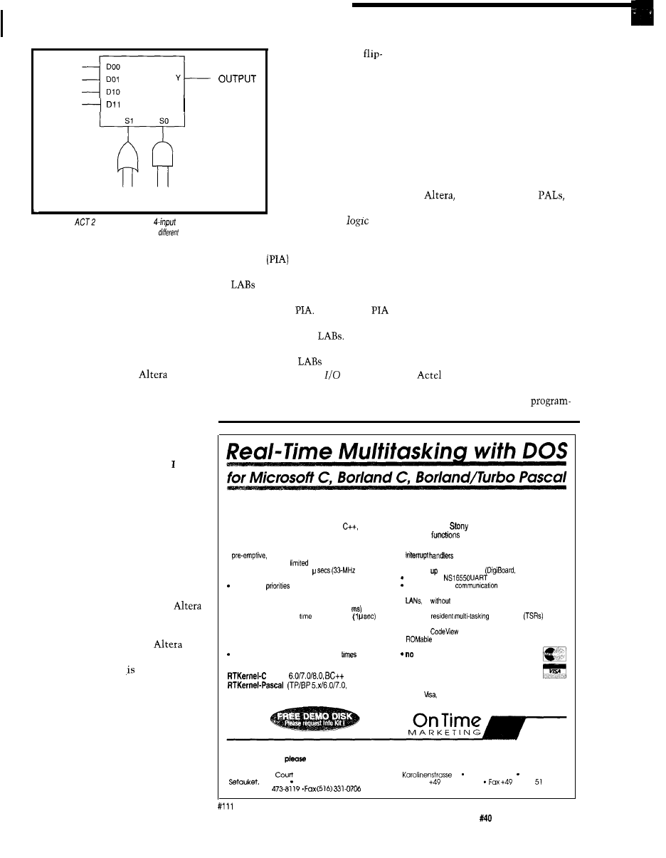
I N P U T S
I N P U T S
Figure 5-The
C-module uses a
multiplexer along with
gates
on the selection pins to implement
logic functions.
Altera designs the chips and does the
layouts and another company, the
“foundry,” actually manufactures the
ICS.)
Altera has developed a few
different families of FPGAs, starting
with the MAX (Multiple Array matrix)
5000 family, then continuing with the
MAX 7000 family, which is currently
very popular. Last year,
intro-
duced the FLEX (Flexible Logic
Element matrix) 8000 family, which is
not structured like a PAL, but instead
uses programmable blocks of logic
based on lookup tables. Those readers
familiar with Xilinx FPGAs will
perhaps recognize the concept. will
cover this later for those who are not
familiar with these chips.
Referring to Figure 3,
16 macrocells are
combined into larger
blocks called a
array block
(LAB). The
programmable intercon-
nect array
routes the necessary
signals between these LAB
S
. Because
all
have dedicated inputs and
routing resources, most signals will
not travel on the
Instead, the
is only used as necessary to share
signals with the other
I will not discuss the MAX 5000
here because it is similar to the MAX
7000 family, but not as powerful or
popular for new designs. The MAX
8000 family is somewhat similar to
the Xilinx family of FPGAs, which I
will discuss later. For now, let’s look
more closely at the MAX 7000 family.
As I mentioned previously,
FPGAs contain groupings of logic that
perform an AND-then-OR function
with certain other options.
calls
these PAL-like modules
macrocells.
Figure 2 shows what contained in
the MAX 7000 macrocell. Five product
terms can be generated in the logic
array, and the product-term select
matrix determines if these signals go
to the OR gate, XOR gate, or instead
are used as register control signals.
Signal inversion can be accom-
plished with the XOR gate and
registering of the signal is possible
using the included
flop. The clocking for
this flip-flop can be done
with the global clock or
from a signal generated
in the logic array section
of the macrocell. Simi-
larly, the flip-flop can be
cleared globally or
locally.
The entire FPGA is thus made up
of interconnected
and one other
type of block called the
control
block.
The I/O control blocks are used
to bring in signals from the external
pins of the FPGA or send signals from
the logic to the pins. The block
configures that pin as input, output, or
bidirectional.
The structure of this chip allows
for fast and predictable operation due
to the uniform structure of the
interconnects. You will see that with
other styles of FPGAs, it is harder to
know in advance what the worst-case
wiring delays will be.
unlike most early
chose not to rely on fuse-based
technology to program the intercon-
nections. They originally decided to
use EPROM-like technologies that
allow for the connections to be erased.
This allows for reuse of these FPGAs.
They now also offer chips that use
static-RAM cell based designs, as well
EEPROM technology.
DIFFERENT FPGA LOGIC
STRUCTURES
Meanwhile other companies such
as
and Xilinx (and later
Crosspoint, QuickLogic, and others)
took a different approach to
Develop Real-Time Multitasking Applications under MS-DOS with RTKernel!
RTKernel is a professional, high-performance real-time multitasking kernel. It runs under MS-DOS or in ROM
and supports Microsoft C, Borland
Borland/Turbo Pascal, and
Brook Pascal’. RTKernel is a
library you can link to your application. It lets you run several C
or Pascal procedures as parallel
tasks. RTKernel offers the following advanced features:
l
event/interrupt-driven scheduling
l
for keyboard, COM ports, and
l
number of tasks only
by available RAM network interrupts included with source code
l
task-switch time of approx. 6
466)
l
supports to 36 COM ports
Hostess boards)
l
performance is independent of the number of tasks
full support of
chip
use up to 64
to control your tasks
fast, inter-network
using Novell’s IPX
l
priorities changeable at run-time
l
runs under MS-DOS 3.0 to 6.0, DR-DOS,
l
time-slicing can be activated
or
operating system
l
programmable timer interrupt rate (0.1 to 55
l
DOS calls from several tasks without re-entrance problems
l
high-resolution timer for
measurement
l
supports
applications
l
activate or suspend tasks out of interrupt handlers
l
runs Windows or DOS Extenders as a task
l
programmable interrupt priorities
l
supports
and Turbo Debugger
l
supports math coprocessor and emulator
l
l
semaphores, mailboxes, and message-passing
l
full source code available
keyboard, hard disk, and floppy disk idle
run-time royalties
usable by other tasks
l
free technical support by phone or fax
(MSC
1.0/2.0/3.x) $495 (Source Code: add $445)
SBP 6.x) $445 (Source Code: add $375)
For international orders, add $30 for shipping and handling. Mastercard,
check, bank transfer, or COD accepted.
Professional Programming Tools
In North
America,
contact:
Outside
North America, please contact:
LEL Computer Systems On Time Marketing
20 Canterbury
32 20357 Homburg GERMANY
NY 1173.3 USA Phone
40 43 74 72
40 43 96
Phone (516)
CompuServe 100140,633
The Computer Applications Journal Issue
November 1993 2 9
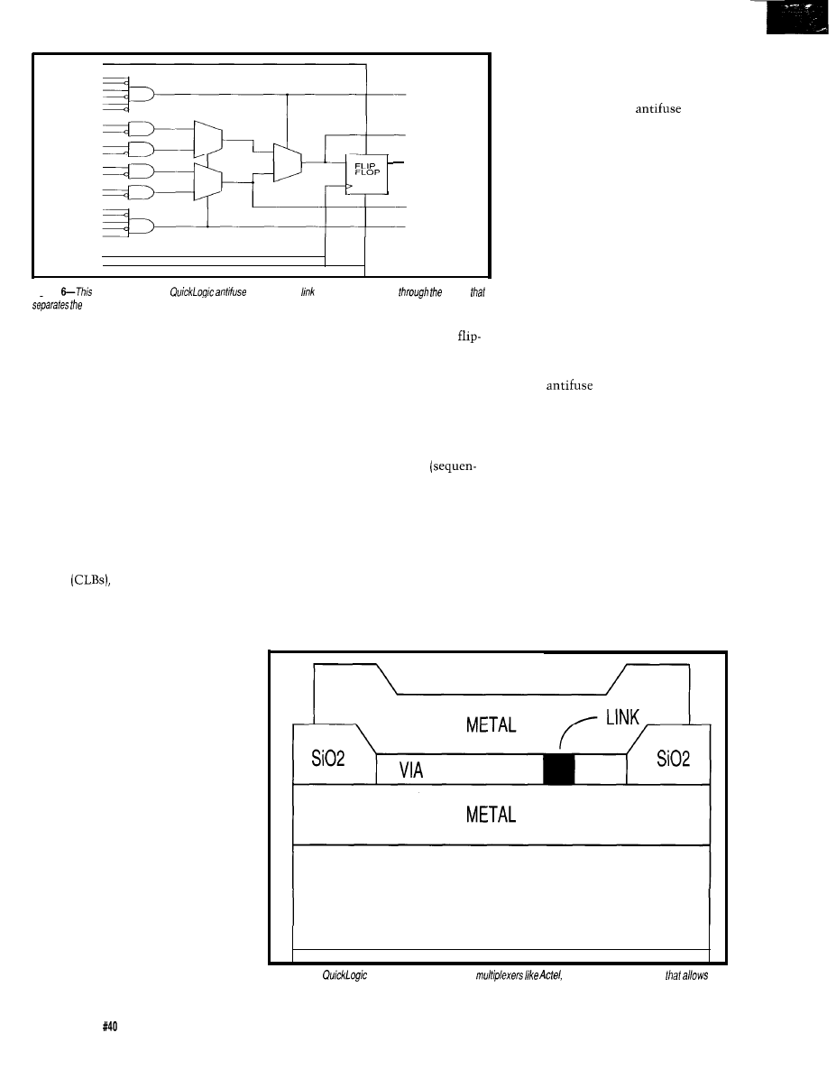
INPUTS O U P U T S
path where a connection is desired. In
this way, the logic cells are pro-
grammed for the function they will
perform and the wiring is set up to
interconnect them. The drawbacks in
some of the early chips concerned
their reliability and speed. The
the inputs and outputs. Registering of
signals in the I/O module is only
available in the ACT 3 family.
Actel chose to use
technology that uses a low-resistance
connections formed during program-
ming were not as reliable as many
Figure
cross-section of a
shows how a
is formed by burning
silicon
people wished. Also, the resistance of
two metal layers.
the connections coupled with the
mable logic. They decided that the
best way to implement programmable
logic is to get away from a matrix of
AND and OR gates and instead use
smaller groups of logic that can then
be wired together.
Each little logic block receives a
limited number of terms and generates
only one or two output terms. These
blocks are then placed in a matrix
pattern and programmable wiring that
runs in between them connects them
together to form the completed chip.
Actel calls their blocks modules,
Xilinx calls them configurable logic
blocks
and QuickLogic refers
to them as logic cells. The main
difference between them all is the
complexity of the logic blocks and
how many inputs can be operated on
simultaneously.
ACTEL
Actel started with the ACT 1
family of FPGAs and has since come
out with the ACT 2 and ACT 3
families. The biggest change occurred
with the ACT 2 family, which packs
more logic into each module.
The modules for the ACT 1 family
are multiplexer based and can imple-
ment any AND, NAND, OR, and
NOR gate possible (up to four inputs)
while inverting any or all of the
inputs. Each of these gates requires
only one module. Certain other
combinations of AND-then-OR and
OR-then-AND are also possible in
only one module. Some of these are
shown in Figure 4. D-type flip-flops,
JK-type flip-flops, and a two-input
multiplexer followed by a D-type
flop are possible, but these require two
modules each.
In the ACT 2 and ACT 3 families,
the modules were modified to allow
more flexibility. One of these is called
C-module (combinatorial module) and
is shown in Figure 5. Another type of
module called the S-module
tial module) is made of a C-module
followed by a flip-flop. These two
modules are supplied on the Actel
FPGAs in equal numbers in an array.
A medium-sized ACT 2 part (the
A1240) has
14
rows and 62 columns of
these modules with up to 104 I/O
lines. The I/O modules (not shown)
can implement bidirectional and
tristate functions as well as latching of
inherent capacitance of integrated
circuit paths created a limit on the
maximum speed at which the chips
could operate.
As
technology grew up,
reliability increased and the connec-
tion resistance fell, making it possible
to run the Actel chips faster and more
reliably than before.
QUICKLOGIC
QuickLogic FPGAs were devel-
oped to address the need for speed.
They accomplished this by using a
lower-resistance antifuse than Actel.
The antifuse structure is shown in
Figure 6. It requires an added process-
ing step to a standard 1 -micron CMOS
gate array process involving the
deposition of amorphous silicon into
Si02
Figure 7-The
logic cell uses gates and
but in a different structure
for
more inputs and outputs.
32 Issue
November 1993 The Computer Applications Journal

the gap between two metal layers.
During programming, this layer allows
for a metal-to-metal junction with a
typical resistance of less than 50 ohms.
The logic module shown in Figure
7 is called a logic cell. This cell from
the QuickLogic 1 family of FPGAs is
similar in structure to the Actel S-
module, but is more complex due to
the addition of logic on the input to
the multiplexers. It also can operate on
up to 14 terms at once, although in
practice this is rarely used. The size of
the array of cells in a QuickLogic
FPGA varies, but the FPGA with 104
has an array of 16 by 24 cells.
CROSSPOINT
Taking the concept of simple logic
modules to the extreme is the transis-
tor-pair-based module in Crosspoint’s
FPGAs. This module makes the
structure very similar to gate arrays,
where the logic is defined and imple-
mented at the transistor level. In fact,
a simple pair of p- and n-channel
transistors make up a transistor pair
tile
which is one of the two
types of “tiles” that form the FPGA. A
typical gate, like a 3-input NAND
gate, requires four of these tiles.
The other type of tile is a RAM-
logic tile (RLT) that is used to make
memory structures, multiplexers, and
exclusive OR and NOR gates.
The chip architecture is called a
channeled gate array structure. It
contains logic rows and routing
channels between these logic rows
where most cell-to-cell connections
are made. Just like the Actel and
QuickLogic FPGAs, Crosspoint uses
antifuse technology for one-time
programmability.
The Crosspoint FPGA structure is
defined on a very fined-grained level
and thus requires a lot of software
intelligence to determine the routing
of interconnections. At present, the
logic for the designs can be entered
into a PC, but the final steps require
software that at present only runs on
Sun or HP-Apollo workstations.
XILINX
Xilinx was one of the first FPGA
companies and is still the most
popular. They started with the Xilinx
2000 family and have since introduced
the 3000 and 4000 families. With each
generation, the logic modules (called
configurable logic blocks or
have become more and more complex
They also recently introduced a line of
FPGAs which have a structure similar
to the
FPGAs.
Figure 8 shows the configuration
of a 3000 family CLB. It looks very
complicated, but the basic operation is
simple to understand. The combinato-
rial function block implements any
function of the allowed variables that
feed it because it is based on a lookup
table. This means all combinations of
input signals have been prepro-
grammed to give the proper output.
In many cases, the combinatorial
logic block accepts five variables: A, B,
C, D, and E. However, the function
block may also use the output of the
flip-flops (QX and QY)-but at the
exclusion of other terms-for a
maximum total of five terms. The
combinatorial function block can also
implement two different functions of
four variables, as long as both func-
tions have certain input variables in
common.
I don’t want to find out how can save a lot of money using
ROM-DOS 5 instead of
in our 80x86 product line.
I don’t care if ROM-DOS 5 is compatible with
MS-DOS 5
but
costs much less.
like
spending much more than I have to.
It makes me feel like a philanthropist and besides Microsoft@
probably needs the money more than I do anyway.
q
IYes, I
want to know the facts about ROM-DOS 5.
Please send me information and a free bootable demo disk to
try with my software.
the
U.S.A.
or
fax this coupon to (206) 435-0253.
Name
Company
State
Phone Fax
Zip
307 N.
OLYMPIC. SUITE 201
l
ARLINGTON. WA 98223 USA
l
l
FAX:
trademarks of
Corporation
The Computer Applications Journal Issue
November 1993 3 3
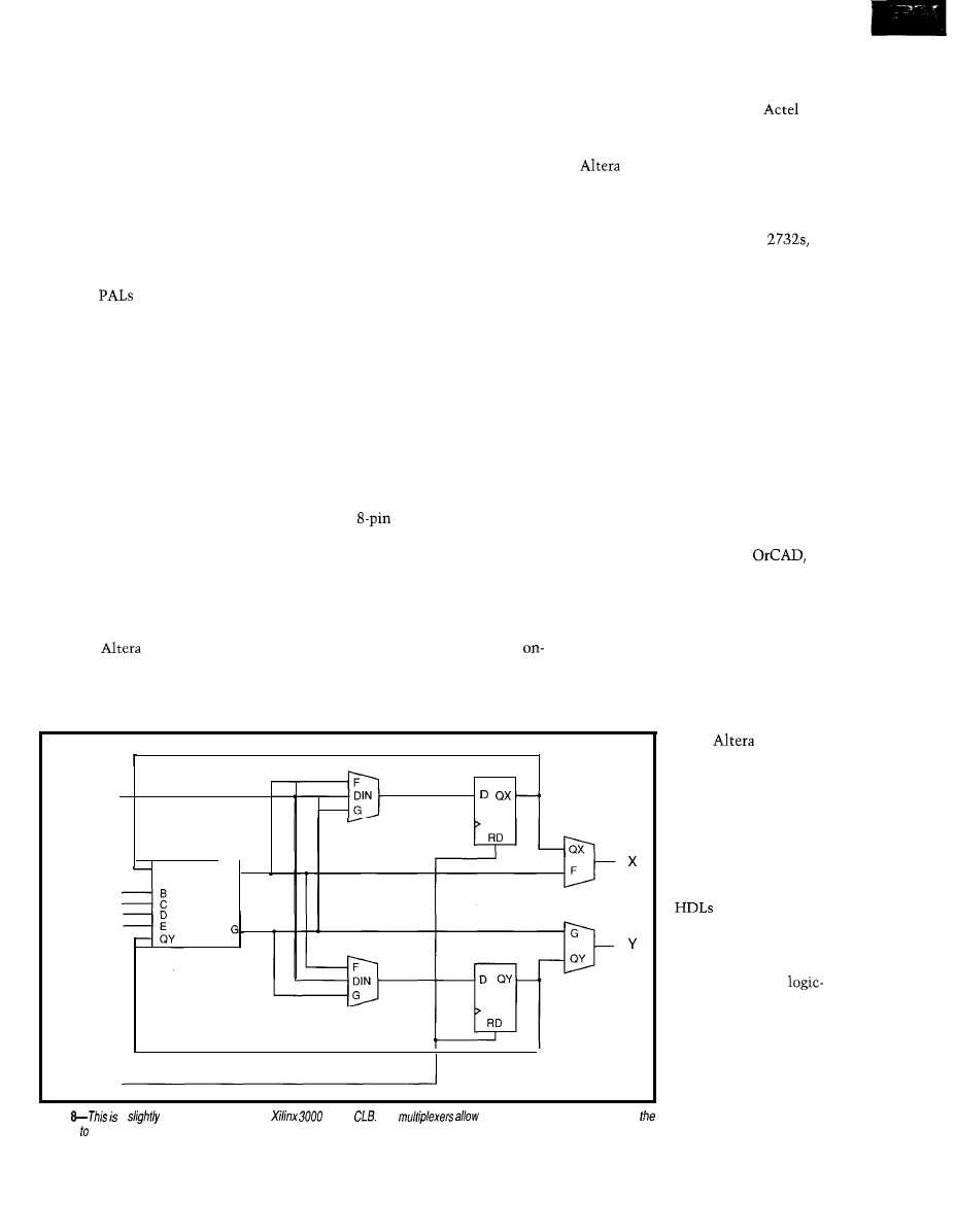
This can sound complex, and it is
a relief to know that as with all
FPGAs, a user does not have to make
decisions on how the block is ar-
ranged, what variables feed it, or even
what a CLB (or macrocell or module or
logic cell) does! The software is
designed to handle all the partitioning
of the logic, the placing of the logic
into different blocks, as well as doing
the routing when the design is fin-
ished.
Like
and other FPGAs, there
is a range of output options in each
Xilinx CLB such as registered outputs
[putting the output of the combinato-
rial function block through a flip-flop),
an inverted clock (so the outputs are
registered on the falling edge of the
clock), asynchronous resets for the
flip-flops, and others.
Xilinx interconnect technology
differs from all the previous FPGAs
discussed. The interconnections are
made by using CMOS transistors as
pass gates that either pass or block a
signal. They are not permanently
wired to do this-it always depends on
the logic level applied to the gates of
the transistors.
Xilinx and the newer FLEX 8000
family of
FPGAs use a static-
RAM based technology very similar to
the methods of a static-RAM chip. In
other words, they use flip-flops to hold
information. This information is
applied to the gates of the transistors
that determine the interconnections as
well as the logic itself.
Because it is static-RAM cell
based, when the power is removed
from the chip, all the interconnection
information is lost. As a result, some
external device (like an EPROM) must
contain this information and the data
must be loaded into the chips every
time the chip has power applied. This
is precisely why they are such good
chips for many applications! Because
they are not one-time programmable
devices, you don’t have to throw them
away everytime you decide to change
the internal logic. On the other hand,
the storage chip increases the board
space required as well as the chip
count.
Xilinx FPGAs have internal logic
that can load the necessary informa-
tion from a standard EPROM or a
special
DIP storage device. It can
also be sent this information from
another source such as a microproces-
sor (that may already be in the system)
with storage capabilities of its own.
This is an application where static-
RAM based devices can really shine.
By changing a single EPROM, an
board microcontroller can be updated
with new software and the logic in the
FPGAs can be changed as well!
Important for experimenters,
though, may be that an expensive
programmer is not required.
and
QuickLogic chips require a special
programmer to burn the antifuses, and
similarly uses an expensive
programmer to set up the EPROM-like
cells. All that is required for a Xilinx
design is a standard EPROM program-
mer capable of programming
2764s or other, similar devices.
DATA
IN
LOGIC
INPUTS
QX
-
A
F-
RESET
SOFTWARE TOOLS
Early programmable logic devices
became popular when the software
tools made it easy to use them, and
FPGAs also rely heavily on the
software tools that take a design and
generate the programming files.
Each FPGA company has its own
development tools, and many FPGA
manufactures also work closely with
third-party software vendors to provide
interfaces with commonly used design
entry tools so that implementing a
design is as painless as possible.
Interfaces are available for
Viewlogic, Mentor Graphic, and other
popular packages. The human-readable
source code for these components is
known as a Hardware Description
Language, or HDL.
Besides interfaces, FPGA compa-
nies and other vendors usually have
tools that allow for entry methods
other than schemati-
cally.
sells a
hardware description
language (AHDL) that
allows for a complete
design to be entered and
simulated without ever
placing a gate. Many
companies are providing
VHDL options as well.
are a great way to
enter a design because
the logic is generated for
you automatically. The
down side is that
generating software is
expensive.
Figure
a
simplified version of the
family
The
for either the combinatorial logic or
flip-flops be used alone. The flip-flops can be reset and clocked from either local or global signals.
Until very recently,
many thousands of
dollars could be spent to
buy the vendor-specific
software necessary to
compile a design, even
3 4 Issue MO November 1993 The Computer Applications Journal
if the design is initially entered into a
third-party schematic-entry program.
Some FPGA vendors such as
Xilinx and Actel realized that the
software tools need to be less expen-
sive for wider use, so they have come
out with basic starter packages for
under $1000 that provide all the
functionality required but some have
limitations on which chips they work
with. Even with the limitations, these
packages have started to open the
market to experimenters and smaller
companies to put these useful chips to
work.
SEE YA LATER, PAL
Having covered the basics of
we are now ready to look
seriously at implementing a design.
My personal requirements when I was
choosing which FPGA included the
need for a programmer that I already
had available at home (an EPROM
programmer), inexpensive software,
and an FPGA that would forgive my
lack of logic simulation and allow me
to reprogram it. Because Xilinx offers
some inexpensive software tools and
the design can use an EPROM to
contain the logic information,
I
selected a Xilinx 3000 family part.
In the next article, will go
through the complete procedure for
implementing a design in an FPGA.
The design will be entered into
and then compiled using
Xilinx software to complete the
design. The FPGA will be used to
create a unique clock with all the logic
on one chip!
Del Hatch is an electrical engineer at
Sandia National Laboratories. In
addition to tracking down project
funding, he has developed micropro-
cessor and FPGA applications for
control
Actel Corp.
955 E. Arques Ave.
Sunnyvale, CA 94086
(408) 739-1010
Fax: (408) 739-1540
Corp.
2610 Orchard Pkwy.
San Jose, CA 95
(408) 894-7000
Crosspoint
5000 Old Ironsides Dr.
Santa Clara, CA 95054
(408) 988-1584
Quick Logic
2933 Bunker Hill La.
Santa
CA 95054
(408) 98
Xilinx Corp.
2100 Logic Dr.
San Jose, CA 95124
(408) 559-7778
404 Very Useful
405 Moderately Useful
406 Not Useful
We’re Small We’re Powerful,
And
Cheaper.
MMT-188
E B
2
serial
ports
3 programmable parallel
RAM/ROM
capable
powerfail detect interrupt
and reset
counter-timers
watch dog timer
expansion connector
In fact, you’ll get the best product for about
half the price. If you’re interested in getting the
most out of your project, put the most into it.
For the least amount of money.
Call us
complete data sheets, CPU
options, prices and
Work
Welcome. Call or fax for
complete data sheets
2308
East Sixth Street
SD 57006
Phone
We offer a full line of low cost
embedded
controllers and software tools which are ideal for
developing products, test fixtures and prototypes.
Features Include:
Low
power
CMOS design
Up to
of code space and
up to 60K of data space
5 to
15 volt operation
Small form factor (3.5”
l
6.5”) with prototyping area
System diskette includes application notes
. Start at $100
Available Options:
Multifunction Board adds A/D, 24
lines and more!
l
BASIC-52 or Monitor/Debugger in EPROM,
l
C Compiler $100 or BASIC Compiler for $300
Iota Systems, Inc.
POB 8987
l
Incline Village, NV 89452
PH: 702-831-6302
l
FAX: 702 831-4629
The Computer Applications Journal
Issue
November 1993
3 5
Loader31
A Pseudo
EPROM
Emulator
Brad Hunting
developed embed-
you are familiar with the
code-burn-try-erase cycle of debugging.
The algorithms are well thought out
and thoroughly tested off-line. The
hardware timings are checked against
the data books. Now comes the time
to put the software and hardware
together and see what happens. You
burn a ROM and try it. Then you find
that subtle defect you missed in
testing. That’s okay, though, because
it’s easy to fix the bug, burn another
ROM, and try again, and again, and
again. After you have been through
this loop a few times you start to think
“there has to be a better way.”
Next you start thinking about
ROM emulators. ROM emulators are
hardware devices that plug into
existing ROM sockets and allow
downloading of hex code into the
emulator without burning an EPROM.
They usually have a serial or parallel
connection to a PC host and some
software to allow downloading of hex
code to the emulator. ROM emulators
are available in sizes from a few
kilobytes to multiple megabits and can
emulate most EPROMs. Prices range
from around a hundred dollars at the
low end to close to a thousand dollars
at the other extreme. Different
emulators will provide different added
features, including cases, power
supplies, the ability to daisy
but all provide the same basic ability
to download code.
LOADER31
An alternative to an expensive
ROM emulator is to use existing target
hardware, mix in a little custom
software, and duplicate the functional-
ity of a ROM emulator. This article
describes how to get the main func-
tionality of a ROM emulator-namely
the ability to download hex code-on
an 8031 system for only the cost of an
SRAM and a socket. I’ll present a
simple hardware target which imple-
ments the necessary memory decod-
ing, and I’ll follow up with a discus-
sion of the software that performs the
loading of the code under test.
Since this method will not work
for all situations I will mention a few
of the limitations first. The method of
ROM emulation I describe works by
mapping RAM space into code space
and then downloading hex code to the
RAM for execution. The main implica-
tion of this method is that the system
under test must have at least as much
unused RAM address space as the size
of the downloaded code. The system
must also be able to map RAM space
over ROM space and must be able to
execute instructions out of the
remapped RAM space. This second
criterion is easily accomplished on an
8031, but the first constraint is
entirely application dependent.
The final constraint for existing
systems is that there must be some
method of interfacing the new RAM
into the system. Therefore, this
method may work better for new
designs rather than as a solution for
existing designs.
The hardware design I presented
here implements the memory map
shown in Figure 1. The ROM area up
FFFF
RAM
8 0 0 0
c s 7 7 x x x
CS 6
c s 5 5 x x x
EPROM
c s 4 4 x x x
c s 3
c s 2 2 x x x
RAM
RAM
c s 0 o x x x
Figure l--The lower 32K
of code space contains the
loader code and any stable application code.
lower
32K
of data space contains the application
RAM
and decoding.
upper 32K of
memory is
used for code to be debugged.
36
Issue
November 1993
The Computer Applications Journal
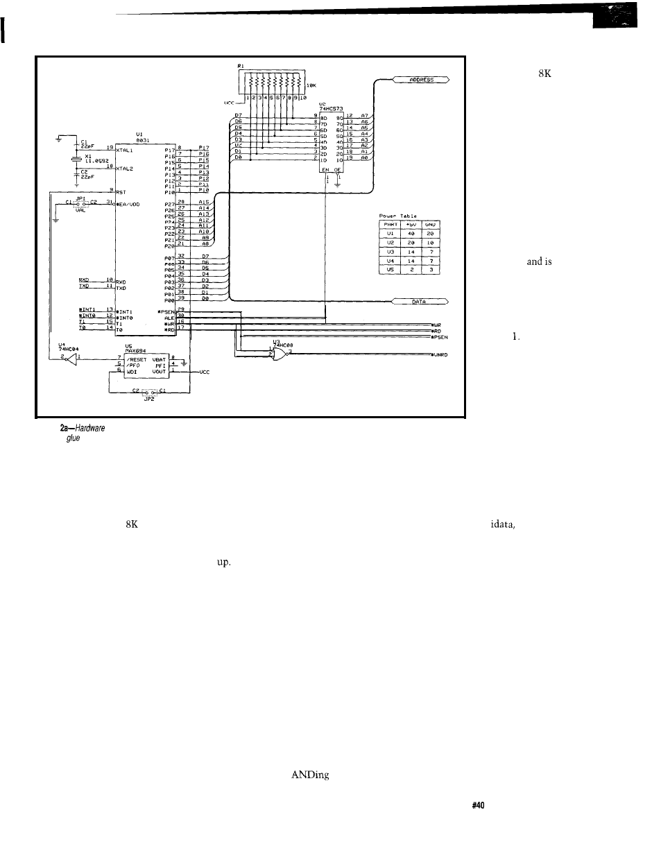
Figure
for loader331 consists of an 8031 microcontroller, a MAX694 for power monitoring and watchdog functions, and a
handful of
logic.
to
32K
is used for the system loader
and any application code that is
known to be stable and defect free.
The RAM area up to 8K is used for
system and application data space. The
RAM space between
and 32K is
decoded on 2K boundaries for external
I/O. The address space above 32K is
mapped with ROM and RAM occupy-
ing the same space and is used for
ROM emulation and code download-
ing.
HARDWARE
The first thing you’ll notice about
the hardware when you look at Figure
2 is that there is nothing particularly
noticeable. The hardware looks just
like the standard 803
1
target that has
been presented dozens of times before,
which is exactly the idea. This
technique is not about any special
hardware; it instead shows a way to
use familiar hardware more effectively.
The only particular item of any
interest is the MAX694 used for power
and RD lines
together. The
of
data RAM, located
at OOOOH, is ac-
cessed as xdata only.
ROM program space
starts at OOOOH and
extends for 32K.
SOFTWARE
It’s
the software
that turns this
average target
hardware into a
pseudo ROM
emulator. It is called
Loader31
available for down-
load from the
Circuit Cellar BBS.
The main routines
are written in C for
the 805 There is
one page of startup
code written in
assembler. The code
and
MAKE
files were
written to use the
Franklin 805 1 C
development tools.
The C code should
be portable to just
monitoring and watchdog timer
functions. I am a believer in watchdog
circuits for embedded controllers. I
have seen controllers lock up in the
field and as inconvenient as it is to
have a system restart in the middle of
a job, it is even more inconvenient to
have a system lock up and stay locked
A nice feature of the MAX694 is
that if the WDI input is left uncon-
nected (JP2 is open), the watchdog
timer function is disabled. If the WDI
input is pulled high or low and kept in
that state for more than
1.5
seconds,
then a reset will be generated. This
allows the watchdog to be disabled for
early development and later reenabled
for field deployment. Of course, for
low-cost systems, the reset circuit can
be replaced by a simple RC circuit.
The target presented in this article
has 32K of overlay RAM located at
8000H. Overlay RAM is accessed as
either xdata or program space. This is
accomplished by
the PSEN
about any C compiler.
Pointer implementation is the
only area that might cause some
problems when porting the code.
Given that the 8051 has five different
address spaces (data,
pdata,
xdata, and code), you must take care to
be sure that pointers are clearly
distinguishable and indicate the type
of memory accessed. This is usually
accomplished by using three byte-sized
pointers. Two of the bytes are used for
the address and the third byte contains
a number to indicate which memory
type the pointer points to.
Loader31
makes extensive use of
pointers, so pointer initialization and
use should be checked carefully when
porting the code. The startup code
might need minimal modification
depending on the naming convention
used by the C compiler for jumping to
the main routine. The
MAKE
file will
have to be modified for each individual
system to indicate the location of the
code and compiler tools.
The Computer Applications Journal
Issue
November 1993
3 7
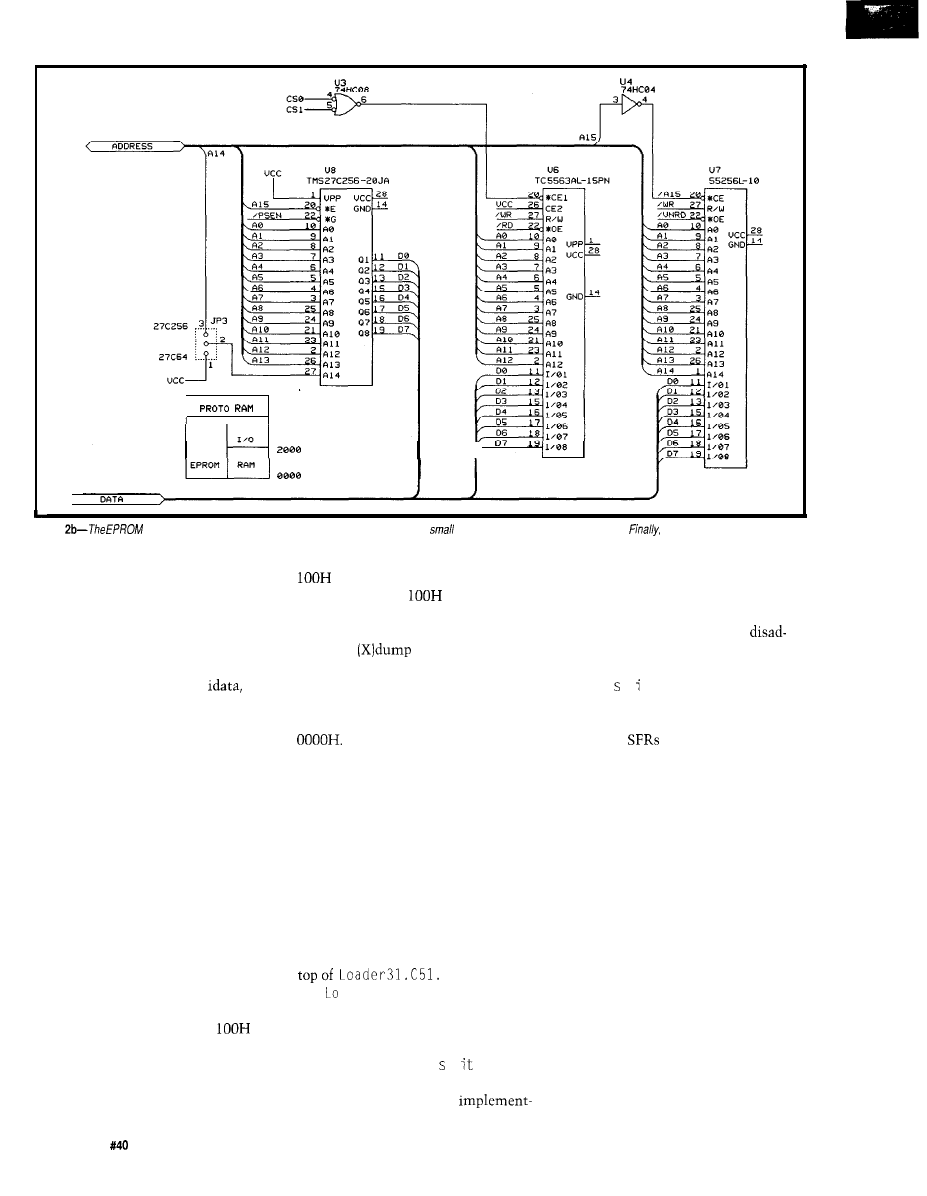
FFFF
I
8 0 0 0
MEMORY MAP
Figure
contains
the system loader and any stable application code. The
RAM chip contains application storage.
the large RAM chip holds the
code to be debugged.
Loader31 code provides the basic
features needed to confirm that a
target is up and functioning properly.
The loader provides the ability to
examine and modify xdata memory,
examine and modify the special
function registers, examine
download Intel hex code, and jump to
a specified address. See Figure 3 for a
list of menu options. Lo ad e r 3 1
occupies a little over 6K of ROM
space, so it will fit comfortably in a
2764 EPROM. Lo a de r 3 1 uses the first
256 bytes of the xdata RAM. Applica-
tion code should only use the RAM
space above 1 OOH.
When writing code to be down-
loaded to the overlay RAM, a few
specifics should be kept in mind. First,
the code must be relocated to start
above 8030H. The overlay RAM starts
at 8000H and Lo ad e r 3 1 uses the first
few bytes of RAM for interrupt
redirection.
The second fact to keep in mind is
that Loader31 uses the first
bytes of xdata RAM. Application code
should not use this area. If an error
occurs and Lo a de r 3 1 must be reen-
tered, Load e r 3 1 will write to the first
using the
command.
bytes. If the application variables
are located above
when
Lo a de r 3 1 is reentered, then the
application variables can be examined
Third, compiler initialization and
startup code must be examined to
ensure that there are no conflicts with
loading the application code above
vantage of this method is that overlay
ing the SFR modification is to write
memory must exist. The advantage of
using the
w t. c
h statement is that
mov and ret instructions out to
Loader31 can be used to start up a
fresh system without any overlay
overlay memory and then perform a
RAM, and
can still be modified.
c a 1 1 to overlay memory. The
Fourth, if interrupts are to be
An area of particular difficulty was
handled in higher levels of code, then
getting the jump to xdata address
care must be taken to initialize the
working. As I mentioned earlier,
memory area between 8000H and
working with pointers for the 805 1 can
8030H. Loader31 redirects interrupts
be a trial. The compiler keeps track of
to this area to enable the application
pointer types and will not allow
code to capture them. I’ll come back to
arithmetic operations of pointers with
this in a moment.
basic types.
Lo ad e r 3 1 is hardcoded to expect
the serial port to run at 9600 bps. This
can be changed by modifying values
placed in the timer1 register near the
INTERRUPT REDIRECTION
a de r 3 1 provides the ability to
display and modify the special func-
tion registers. Modification of the
special function registers is accom-
plished by using a large w c h
statement with an entry for each SFR.
An alternative method of
The 803 1 is hardwired in silicon
to jump to addresses within the first
35 bytes of program space in response
to different interrupts. This forces the
interrupt handler routines to reside in
low memory. In order to allow user
applications to handle interrupts,
Lo a de r 3 1 redirects the interrupts to
overlay RAM by placing a long jump at
each of the hardwired interrupt
38
Issue
November 1993
The Computer Applications Journal
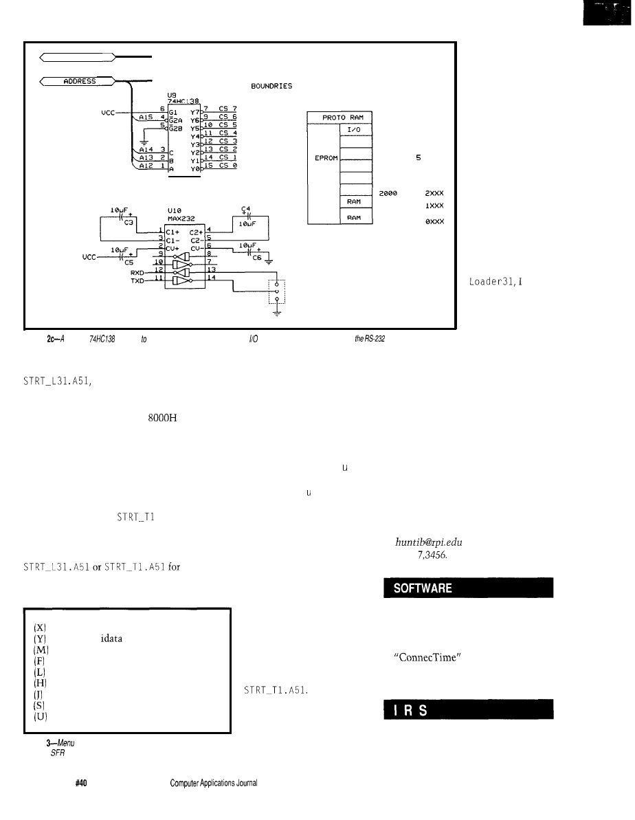
DATA
4K DECODE
FFFF
8000
0000
MEMORY MAP
JUMPER3
cs 7
CS 6
cs
cs 4
cs 3
cs 2
cs 1
cs 0
7xxx
6XXX
5xxx
4xxx
3xxx
Figure
simple
is used
decode the lower RAM and space, while a
MAX232
provides
drivers and receivers.
addresses. The loader startup code,
then writes a RET1 at
each of the targeted interrupt addresses
in overlay RAM. Interrupts are
redirected to RAM addresses
through 8020H on eight-byte bound-
aries. To process the interrupts in the
user application code, the user code
writes over the
RET I
instructions in
overlay RAM with calls or jumps to
interrupt handlers. This can be done
either at load or run time.
The example code,
. A51,
captures the interrupts at load time by
placing jump instructions at the
redirected interrupt locations. See
exact addresses to modify. Interrupt
handlers must end with a
RET I or
interrupts of equal or lower priority
will be blocked. If the interrupt
handlers are written in a high-level
language, a call to the high-level
routine can be placed at the interrupt
target address and a
RET I
placed after
the handler returns.
A special note applies to compilers
that support the keyword i
n t e r r p
t .
If the compiler used to develop the test
code allows the i
n t e r r p t
keyword,
that feature may not be usable in the
Lo a de r 3 1
environment. The compiler
may generate additional initialization
code when the
i n t e r r u p t
keyword is
used. This additional code tries to
initialize the low memory interrupt
vector table which already exists in
the
Loader31
ROM.
Check the output of the
compiler used. If the com-
piler generates the extra
initialization code, then the
method of interrupt handling
shown in the example test
code should be used. See
Tousethis
method, the interrupt
handler is written in the
high-level language as a
Dump xdata contents to terminal
Dump
contents to terminal
Modify xdata location
Fill xdata with a char
Load xdata from terminal
Load an Intel hex file
Jump to xdata address
Display SFR registers
Update SFR registers
Figure
options for Loader31 include displaying and
simple subroutine that
updating
registers.
neither receives nor returns
any values. An
LCA L L
is placed at
the target location
of the redirected
interrupt to call
the interrupt
processing subrou-
tine. When the
subroutine finishes
and returns, a
R ET I
is generated
to enable inter-
rupts and to return
to the interrupted
code.
CONCLUSION
During the
development of
ran
into some prob-
lems with the way
the Franklin
compiler handles
pointers. Luckily,
enough of
Loader31 was
working to allow
downloading of the loader code for
testing. I have already used Lo ad e r 3
1
on a couple of projects and it has
certainly helped reduce the develop-
ment cycle time.
q
Brad Hunting has industrial experi-
ence in embedded systems develop-
ment for equipment automation and
process control. He has recently
returned to school to complete a
graduate degree at Rensselaer Poly-
technic Institute. He can be reached
at
or on CompuServe
as 7265
Software for this article is avail-
able from the Circuit Cellar BBS
and on Software On Disk for this
issue. Please see the end of
in this issue for
downloading and ordering
information.
407 Very Useful
408 Moderately Useful
409 Not Useful
40
Issue
November 1993
The
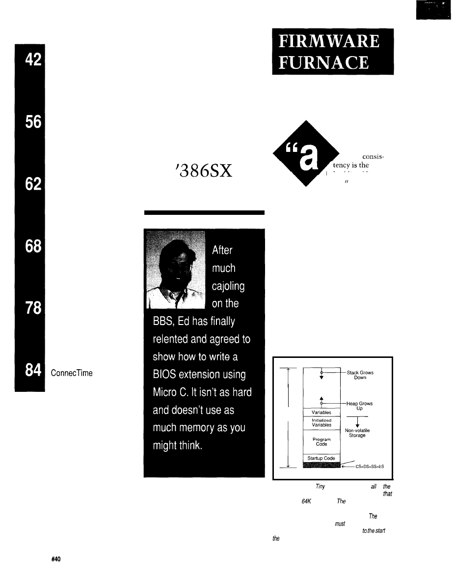
DEPARTMENTS
Firmware Furnace
From the Bench
Silicon Update
Embedded Techniques
Patent Talk
Booting C
Writing a
Micro-C BIOS
Extension for
the
Project
Ed Nisley
foolish
hobgoblin of little
minds..
may
be an
aphorism suitable for any occasion. In
this case, back in Issue 36 I opined that
writing BIOS extensions in C wasn’t
practical because of the Firmware
Development Board’s limited memory
address space. Emerson would smile,
as several conversations on the BBS
changed my mind.
The consensus seems to be that, if
you need just a smidge of code, you
may as well write it in C and be done
with it. After all, it doesn’t matter if
you have 3
1
K of C or 3K of carefully
tuned assembler.. the RAM still has
32K bytes. I can’t argue with that
logic, so this month we’ll explore the
gory details of turning a Micro-C
program into a BIOS extension.
64K
bytes
Maximum
0100 Unused bytes
Figure l--Micro-C’s
memory mode/puts of
program’s addressable storage in a sing/e segment
may be up to
bytes long.
program code and
initialized variables must either be in nonvolatile storage
or copied from diskette by a loader program.
variables, heap,
and stack
be in RAM (for obvious
reasons). All four segment registers point
of
segment.
42
Issue
November 1993
The Computer Applications Journal
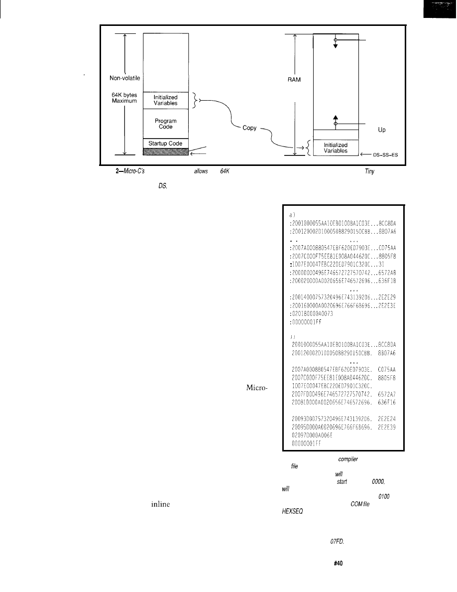
The complexities
along the way may
seem daunting, but
the end result should
help you get your
own code working..
and that’s what it’s
all about!
BASIC BIOS
BOOTING
Every PC goes
through much the
same ritual immedi-
ately after a hardware
reset: check the
hardware, find and
initialize any BIOS
extensions, and
finally boot a program
Storage
0100 Unused bytes
c s
64K bytes
Maximum
Stack Grows
Down
Heap Grows
Variables
Figure
Small memory model
up to
bytes of program code and initialized variables, which, as with
mode/, must
be in nonvolatile storage addressed by the CS register. The startup code, or loader, must copy the initialized variables into a separate RAM
segment addressed by the
SS, and ES registers. Because the initialized variables are copied to RAM they may be changed during the
program’s execution.
from disk. The first time a BIOS
extension gets control happens when
the BIOS searches for and calls each
BIOS extension in sequence. The
extensions must hook interrupt
vectors if they want to be part of the
action after the BIOS regains control.
The exact state of the system isn’t
predictable when your extension gets
control because each extension can
add features or change the BIOS setup
in nearly any way. In any given
system, of course, the same thing
happens (or should happen!) during
each boot, but you cannot assume all
systems respond the same way. For
example, you’d think the serial ports
would be set up before the extensions,
but on my ‘386SX that’s not the case.
After all the extensions are set up,
the BIOS finishes its own initialization
and issues an Int
19
(hex, remember).
Under normal circumstances, that
interrupt vector points back into the
BIOS code to a bootstrap loader routine
that handles booting from either
diskette or a hard disk. Any BIOS
extension, however, can hook Int 19 to
regain control just before BIOS
accesses the disk; the code may check
a serial number, verify a password, or
omit the disk boot entirely.
If the original BIOS Int
19 does get
control in a system with no bootable
disks, it will issue Int 18 after failing
to read the disks. In the Original IBM
PC, that interrupt fired up the built-in
Cassette BASIC interpreter, but clones
don’t have rights to that code, so most
of them simply display a message and
await a three-finger salute. Your BIOS
extension can hook Int 18 to get
control after the disk boot fails, so you
can load one program from diskette or
run another from the extension
without booting.
According to the references, the
system is completely ready for action
by the time Int 19 and, if needed, Int
18 occur. Your extension can take
control of a perfectly functional PC
without having to handle the grubby
setup work. The code this month has a
“your program goes here” note at the
appropriate spot so you can
complexicate it as needed.
MODELING MEMORY
So far we have been using
C’s Tiny memory model, but that
won’t work for a BIOS extension. The
reason, as with most things PC-ish,
involves the segmented memory in
80x86 real-mode programming.
Tiny memory model puts all of
the C program’s code and data into a
single 64K byte segment, as shown in
Figure
1.
All four of the segment
registers must contain the same value:
the paragraph address of that segment.
An assembly language function or
code can refer to memory
outside that segment by reloading the
segment registers as long as they are
restored whenever the C-level code has
control.
a d d i t i o n a l l i n e s
a d d i t i o n a l l i n e s
a d d i t i o n a l l i n e s
a d d i t i o n a l l i n e s
3 1
Figure 3-a) The Micro-C
produces a single
hex containing both the program code and initialized
variables. Because they
ultimately reside in different
segments, both sections
at address
but this
confuse most hex utility programs and file transfer
routines. The code section starts at address
because we are using the DOS
format. b) The
utility program reads the hex file and relocates
the initialized data addresses so it follows the code
section in memory. On/y the addresses and checksums
of the last group of lines must change; in this case the
data starts at address
The Computer Applications Journal
Issue
November 1993
4 3
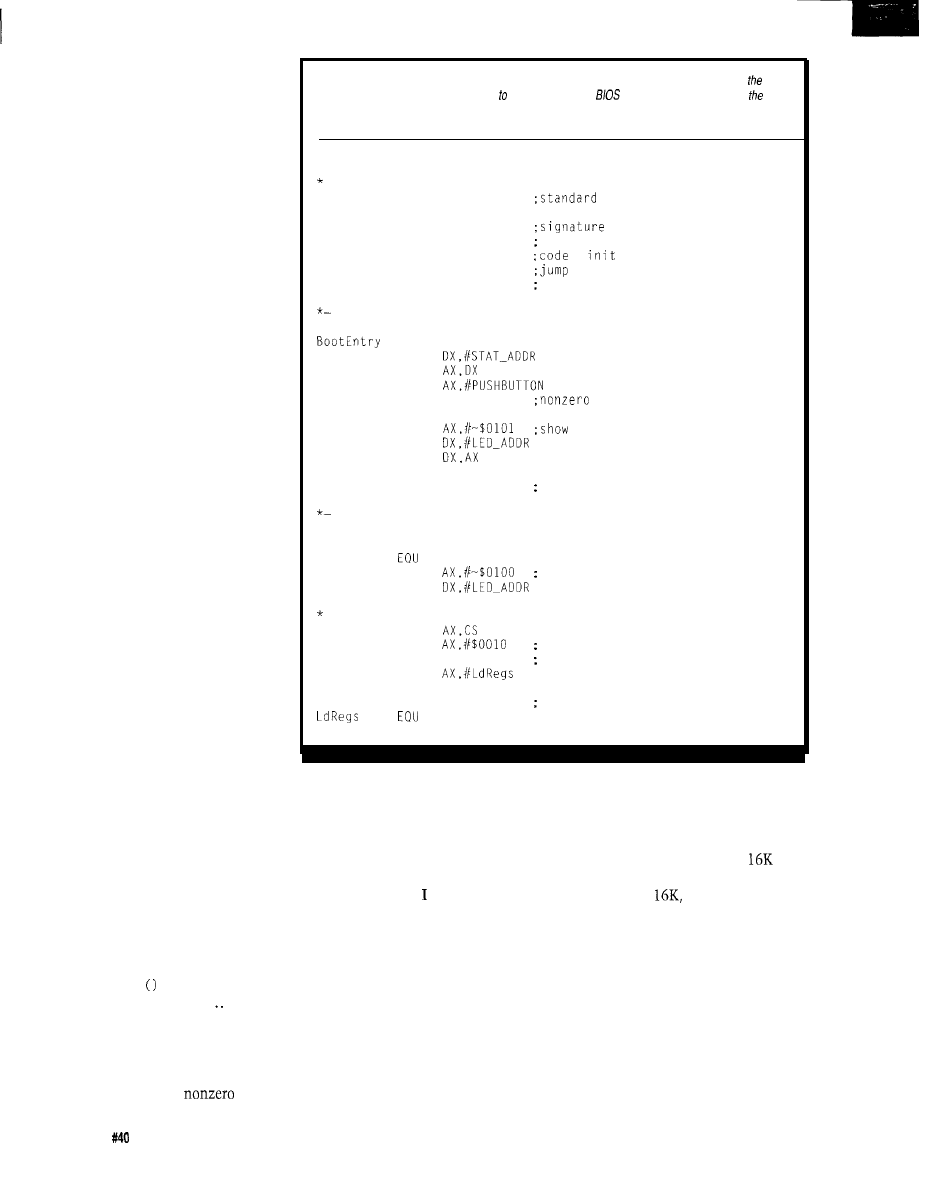
The program’s startup code begins
at offset 0100, followed by the com-
piled C code and library functions. All
of the initialized data, such as strings
and “constant” variables, come next.
Uninitialized variables follow, with
the heap beginning just after the last
variable. The stack grows downward
from the end of the segment, so the
heap and stack together use whatever
space is left beyond the program and
data.
Listing la--The ordinary Small-model Micro-C startup routine assumes it has complete control of
system, so several changes are required adapt it to use as a
extension. This listing shows
header bytes, the pushbutton test, and the CS adjustment needed to make the code offsets work out
correctly.
*
*
BIOS Extension header
ORG
$0100
COM offset
*
Recall that the first 256 bytes of
the segment are a legacy of the DOS
COM-format program structure. While
this format lets us produce and
manipulate the programs with ordi-
nary DOS utilities and compilers, it
wastes those 256 bytes. If you have (or
write!) the utilities to load the program
and set up the registers, Micro-C’s
startup code can begin at any offset.
DB
$55
DB
BAA
second byte
DB 16
+
data (512 byte units)
JMP
<BootEntry
around checksum
DB
$00
which goes here
*
if pushbutton is down, exit without doing much
*
E Q U *
MOV
IN
TEST
JNZ
<Continue
means not pushed
*
A single segment won’t suffice for
the BIOS extension, however, because
the FDB’s battery-backed RAM is
normally write-protected. Putting
variables in write-protected RAM is
bad enough, but trying to run a CPU
with a write-protected stack just won’t
work. The assembler code I presented
in Issue 38 controlled write protection
around each data access and used the
caller’s stack, but that’s impractical for
a C program.
MOV
to track our path
MOV
OUT
*
RETF
return to normal BIOS boot
*
pushbutton is up, so it is OK to continue
*
adjust CS so our offsets are correct
*
Continue
*
MOV
show single here
MOV
OUT
DX,AX
The most straightforward solution
uses Micro-C’s Small memory model,
which allows up to 64K bytes of
program code and initialized variables
in one segment. A second 64K byte
segment holds a copy of the initialized
variables, the ordinary variables, the
heap, and the stack. Figure 2 shows the
Small model segment layout.
MOV
SUB
add 0100 to offsets!
PUSH AX
simulate a FAR CALL
MOV
PUSH AX
RETF
to load the new values
*
*
How this works in our situation
should be evident. The code segment
is the FDB’s battery-backed RAM,
while the data segment resides in
system RAM below the 640K line. The
startup code must reserve the data
segment, copy the initialized variables,
and load the segment registers before
calling the ma i n C routine. It’s just
a simple matter of software..
starting values. In Micro-C’s Tiny
model, these variables are locked in
nonvolatile storage unless you are
booting from diskette into RAM, so
they behave like constants.
There are other ways to solve the
problem, of course. picked Small
model because it worked out quite
neatly and exploited an interesting
Micro-C feature, but another approach
may be more suited for your projects.
As always, take what you read here
and make your own improvements!
Incidentally, because the startup
You could duplicate the diskette
code copies the initialized variables
boot loader’s function for the BIOS
from nonvolatile storage into RAM,
extension: copy the C program from
the C program can treat them as
the FDB’s RAM to system RAM, then
ordinary variables with
execute it using Tiny memory model
just as before. The battery-backed
RAM can thus remain write-protected
during the whole operation.
You might also modify the FDB’s
circuitry to protect the lower
bytes of RAM while allowing writes
into the upper
but it seems a
shame to leave the entire system RAM
unused. Micro-C’s startup code
includes support for such “split”
memory segments, which are more
common in minimal 8086 systems
than PCs. This is, however, a nice
solution if you use a PAL to handle
memory decoding rather than the
FDB’s discrete logic.
For now, however, Small model
will do what we need without any
4 4
Issue
November 1993
The Computer Applications Journal
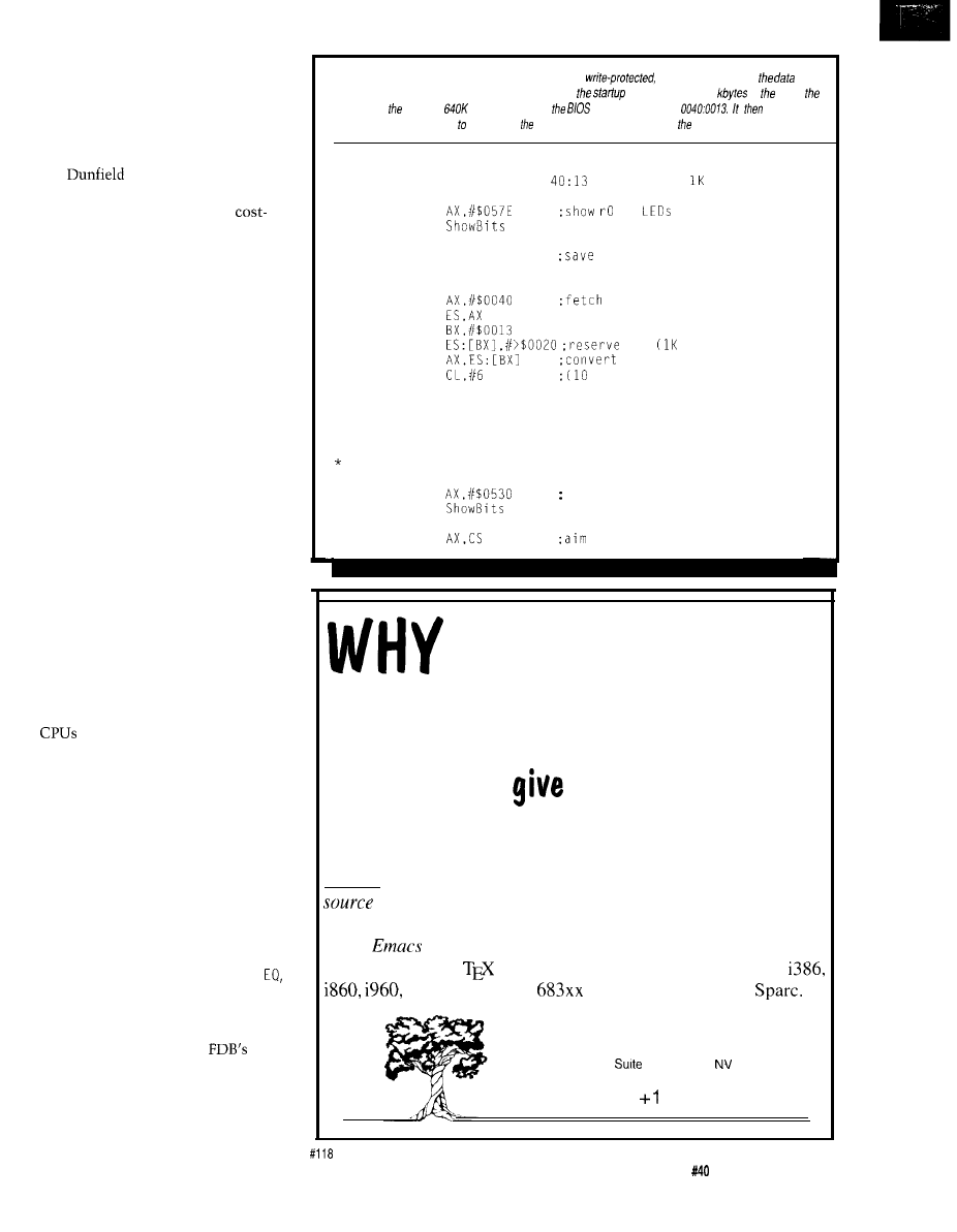
hardware modifications. There is only
one gotcha..
SHUFFLING SEGMENTS
Micro-C was designed as a simple,
portable C compiler for microcomput-
ers.
has adapted it to a wide
variety of micros with striking
success; it’s certainly the best
performance buy on the market. The
8086 CPU, however, stretches the
compiler’s architecture nearly to the
breaking point..
The end result of a Micro-C
compilation is a hex file in either Intel
or Motorola format. In either case, the
maximum file size is 64K bytes
because the address field is two bytes
wide and there is no way to specify
more than one segment. Dave is
planning support for Intel’s extended
hex file format, but the trick I’ll show
you may come in handy in other
situations.
The hex file for a Small model
program contains two sections:
program code and initialized data. The
code section starts at address 0100
because we are using the COM file
format, but the data section starts at
address 0000. The two address ranges
overlap without any way to indicate
that they are in two separate segments.
Figure 3a shows the raw compiler
output file.
Because Micro-C was designed for
without segmented memory,
there is no way for the compiler to tell
the assembler, “This data really has
two addresses: one in this segment and
another in that segment. Use the right
one, please!” The compiler simply
produces an assembler file with the
code and data at the appropriate
addresses in their ultimate segments.
That means we must process the hex
file produced by the assembler to get
what we need.
Rather than tweak the file
manually each time,’ I wrote
H E X S
a
DOS utility to modify the hex file’s
data segment addresses. Because the
initialized data should follow immedi-
ately after the code in the
battery-backed RAM, the job is quite
simple: just add the code’s length to
each data address. Figure 3b shows
what the output file looks like: note
Listing lb-Because the Micro-C exfension code is in
battery-backed RAM,
segmenf must be located elsewhere. This section of
routine reserves 32
at fop of
RAM below infamous
barrier by adjusting
RAM-Size
word at
copies
initialized variables RAM, clears uninitialized variables, and sets up segment registers.
*
locate the data segment at the top 32K of contiguous RAM
* the BIOS RAM size value at
has units of bytes
*
MOV
on
to mark entry
CALL
*
PUSH DS
BIOS seg regs
PUSH ES
;on the BIOS stack
*
MOV
memory size
MOV
MOV
SUB
32K
byte units)
MOV
RAM size to seg reg
MOV
bits left, 4 bits right
SHL
AX,CL
MOV
ES,AX
*
* copy the initialized data to the data segment
* the length is just the offset of ?temp...
as long as ?temp is the first uninitialized variable!
*
MOV
rl
CALL
*
MOV
at this segment
(continued)
are our cross
compilers so inexpensive???
Because we
them away
free!
We base our cross compilers on the GNU C/C++ compiler from the
Free Software Foundation.
We provide you with one year of
support*, and give you a ready-to-run cross compiler with complete
for DOS, Windows, OS/2 2.0 or UNIX for $495 per year.
Or, get the extended support package for $895, which includes
GNU
and make, the CVS and RCS source code control
utilities,
and the
typesetting system. Targets include
Motorola 680x0,
and 88000, MIPS and
Hundred Acre Consulting
5301 Longley Lane
D-144, Reno
89511
(800) 2452885 -702-829-9700
The Computer Applications Journal
Issue
November 1993
4 5
Users!
16 BIT DNA
ACQUISITION?
Settle
Less
Than The Cutting Edge...
HIGH PERFORMANCE
Guaranteed t 6 bit accuracy
6 Channel
Board
l
16 bit ND resolution
l
16 bit
throug put
l 6 lines di
I/O
l 3 channe counter/timer
LOW COST
$1295
16 bit
6 Channel
Board
l
16 bit
resolution
throughput
lines di
channe counter/timer
OPTIMUM CONVERSION
compatible
AID Board
l
16 bit
resolution
l
16 bit accuracy
l
DMA, Prog. Gain
$1395
l
16 lines
I/O
l 3 channel counter/timer
l 2 D/A channels
Cut through the specs each of
bit boards have been evaluated against
every competing model. On noise
performance, speed, ease of use, and price,
leading technology wins every time.
See for yourself Call for an evaluation
board today.
I - 8 0 0 - 6 4 8 - 6 5 8 9
We’ve been making data
acquisition boards for longer
than anyone in the world.
corporation
70 Tower Office Park, Woburn, MA 01801
FAX (617) 938-6553 TEL (617) 935-6668
Analog Digital
Industrial PCs,
and High Channel Count Systems
Listing
lb-continued
MOV
MOV
up offset as length
MOV
of
data in code seg
MOV
to our part of data seg
JCXZ
?nocopy
if zero (or 64 bytes long
REP
MOVSB
to
?nocopy
*
* clear the uninitialized data while we have the pointers at hand
* length is the difference between
and ?temp
* as long as
is just beyond the last variable
MOV
CALL
*
MOV
MOV
around for phase error bug
SUB
CX,AX
MOV
;get a zero (or a test value!)
REP
STOSB
*
* aim DS at the new data segment
*
MOV
MOV
* save the BIOS
registers
* begin using our stack in the new data segment
* store stack location in interruot vector for the C code
MOV
MOV
MOV
MOV
*
XOR
MOV
MOV
ADD
BX,BX
ADD
MOV
MOV
interrupt vector
MOV
ES
that
only the data addresses and
SEQUENCEDSTARTUP
checksums change.
H E
X S
E
is
The C startup code must convert
able on the BBS, but isn’t worth
the BIOS extension entry conventions
further discussion here.
into Micro-C’s
conventions,
The resulting hex file produces,
run the C program, and then return
once again, a simple binary
format program that can be loaded into
the
battery-backed RAM using
the
LOADEXT
boot loader from Issues
36 and 38. After the code is loaded,
BIOS will invoke it each time the
system restarts with no further
attention on our part.
Now, having the big picture in
mind, we can delve into the details of
writing a C-language BIOS extension.
control to the BIOS after the extension
is set up. Coupled with the segment
shuffling required by Small model
code, the startup code has some
interesting tricks.
The extension must start with the
signature required by the BIOS scan, so
Listing la is similar to the code
presented in Issue 38. The diskette
boot loader computes the checksum
on the contents of the disk file and the
46
Issue
November
1993
The Computer Applications Journal
Listing 1 c-Once
variables
segment registers are set up correctly, the remaining code
initializes the Micro-C heap and calls the
function. Unlike most embedded C programs,
must
return so the
can continue the boot sequence. This listing shows how the code restores the segment
registers and returns the BIOS.
now, for the main event..
*
MOV
CALL
*
MOV
CALL
main
*
restore regs and return
*
MOV
MOV
*
POP
ES
POP
*
MOV
CALL
*
RETF
Remainder of Micro-C startup code
up empty heap
main program
;aim back at BIOS stack
BIOS stack
rr to indicate the end
and continue with boot
is unchanged
Listing
2-The
function shown here moves the vector to so we can use if later, then
aims 19 at our own interrupt handler. displays a tracking number on the
but cannot send a
serial message because the
has yet to
the hardware
Because this function is called
during the B/OS extension scan, it must exit to
the PC to continue booting.
main0
move old handler
to new interrupt
return:
values in the battery-backed RAM
beyond the end of the program, so the
checksum byte must be zero in the
source code and disk file.
The extension bails out without
further action if the FDB’s push-button
switch is closed so you can boot the
system without loading the extension.
Recall that I rewired the keyboard lock
switch in parallel with the push
button so you can control this func-
tion without opening the case (assum-
ing, of course, that your case is closed
in the first place!).
The next step adjusts the CS and
IP registers to match the COM
program assumption. The
RAM
is
at
so the initial CS:IP is
The simulated FAR CA L L
reloads CS with
and adds 0100 to
IP so the offsets assumed by the
startup code are correct. Refer back to
Issue 38 for more details on this
trickery.
Next, the code reserves RAM for
the data segment. The BIOS power-on
self tests record the system’s RAM size
(in kilobytes) in the word at
This value does not include memory
above the
line, so a 2-MB
‘386SX system has a RAM size of only
0280 hex or 640 decimal. If your
system has an old CGA card, system
RAM can extend up to address
Data Acquisition
and Control
Without Compromise
Programmable Scan Burst
Advanced Industrial Control
boards set a new performance
standard for general purpose
industrial laboratory applications.
ADA2210 with
A
solution
ADA2210 features:
125
XT throughput
16 SE.
analog inputs
n
selectable input range
programmable auto channel scan
n programmable burst mode
n software external triggers, pacer clock
n on-demand DMA transfer
programmable gain:
000)
I3 cascadable
counters
n 16 programmable digital I/O lines
n two
analog outputs, selectable range
Universal TSR DOS driver
Notebook driver
HARDWARE SOLUTIONS
AIC family also includes AT
analog
boards,
only A/D control boards for
portable PCs, 4-20
current loopoutputs,
and opto-22 compatibility.
SOFTWARE SOLUTIONS
Select the power and performance of
or
from
library of application programs for moni-
toring, data acquisition and analysis, control,
DSP and 3D graphics.
For more
information on these and other
ISA
bus and
products,
call, write
us today!
Place your order now and receive
and
for
Real Time Devices, Inc.
P.O.
Box 906
State College, PA 16804
(814) 234-8087 Fax: (814) 234-5218
The Computer Applications Journal
Issue
November 1993
47
for 736K bytes of contigu-
ous memory, but that trick won’t
work with monochrome or the
standard VGA cards.
The most convenient location for
the data segment is at the top of
system memory. The code in Listing
subtracts 32K bytes from the RAM
size, so any subsequent extensions [or
the embedded program booted from
diskette) will find 608KB of RAM.
Admittedly, 32K bytes is more than
we need, but you can see the general
principle at work.
The next chunk of code copies the
initialized variables to RAM. The
startup code includes a work variable
called ? emp which is always the first
uninitialized variable, so the length of
the initialized block is simply the
address of ?
If there are no
initialized variables, this length will
be zero, so I check the CX register
before starting the REP MO V S B opera-
tion.
The standard Micro-C startup
code does not zero the uninitialized
variables, but I added that feature
because the registers already pointed
to the right place. The ? h
ea p
variable
marks the start of the heap, which
always follows the uninitialized
variables, so the length is just the
difference between
and
?temp.
There will always be at least two bytes
to clear because ?
emp
always exists.
The next step is critical. Up to
this point, the code has been using
whatever stack the BIOS passed to it,
but the C program should run with its
own stack to provide enough space for
nested function calls and interrupts.
The code stores the BIOS’s SS:SP
valuesinthe ?BIOS_SS and
variables so they can be restored on
exit, then reloads SS:SP with a pointer
to the end of the reserved RAM
segment.
Figure 2 shows that the stack
grows downward in the data segment,
so the initial stack pointer aims at the
end of the segment. Because I picked a
chunk of RAM, the initial SP
is 7FFE. If you need a
data
segment, use FFFE. The value should
be two bytes below the end of the
segment to avoid the dreaded trap:
Stack Fault Error.
Listing
macro
wrapper saves the caller’s registers, sets up the segment registers
for a Small-model
C handler, and restores the registers before returning. The code must also save and restore the Micro-C
compiler’s ?temp work location, but this can cause problems if the interrupted code isn’t a Micro-C function.
63
size of prologue code
start of prologue
#define
#define
asm
save bystanders on incoming stack \
fn
PUSH
AX
PUSH
BX
\
PUSH
cx
\
PUSH
ES
\
*- fetch pointer to
segment and stack
\
XOR
\
MOV
\
MOV
\
MOV
\
SUB
\
MOV
\
MOV
XCHG
\
PUSH
cx
\
PUSH
AX
\
*- save remaining bystanders and compiler temp on our stack \
PUSH
DX
\
PUSH
SI
\
PUSH
DI
\
MOV
AX,?temp
\
PUSH
AX
\
PUSH
DS
\
set up seg regs
\
MOV
AX,SS
\
MOV
MOV
\
*- invoke the Micro-C handler
\
CALL
\
restore OS, compiler temp. and bystanders from our stack \
POP
DS
\
POP
AX
\
MOV
\
POP
DI
\
POP
\
POP
DX
\
*- restore pointer to incoming stack
POP
AX
\
POP
cx
\
MOV
\
MOV
restore remaining bystanders
\
POP
ES
POP
cx
\
POP
BX
POP
AX
\
bypass
return
\
\
The next step may seem peculiar,
segment would begin at 9580:0000
but, because our BIOS extension may
rather than 9800:OOO0. But we can’t
not be the first or last extension
store the pointer to the data segment
installed, the data segment’s location
in the data segment..
cannot be hardcoded in the startup
Fortunately, the interrupt vectors
code. For example, if an earlier
between Int 60 and Int 67 are reserved
extension reserved
bytes, our 32K
for user functions. The code stores a
50
Issue
November 1993
The Computer
pointer to the top of the stack in Int
60’s vector. The extension can fetch
the Int 60 vector to find its data
segment, but actually executing an Int
60 is fatal because the vector does not
point to an interrupt handler.
The vector’s segment marks the
start of the initialized variables at
offset 0000. The end of the segment is
always two bytes beyond the top of the
empty stack, so a single vector can
supply three distinct values.
If you’re offended by this trick,
which has considerable precedent in
the BIOS and DOS world, you can put
the data segment pointer at a
coded location in the
backed RAM. That frees a user
interrupt vector, but does require
updating the FDB RAM during each
boot. Again, it’s up to you.
The remainder of the setup
routine is almost anticlimactic, as you
can see from Listing lc. The code
initializes the heap by writing a zero at
?
p, then calls the ma i n
func-
tion. When the routine returns, the
code restores the BIOS
values,
pops the saved registers from the
BIOS stack, and returns to the BIOS
with the obligatory FAR RET instruc-
tion.
Unlike all the other Micro-C
programs you’ve seen so far in this
column, this ma i n
function must
exit so the BIOS initialization can
continue. Because system setup is not
complete, the C program should do no
more than absolutely necessary. In
particular, on my system the BIOS
hasn’t loaded the serial port addresses
at
so ma i n
can’t even
send a “hello” message using the BIOS
serial functions!
If your system has a video card,
monitor, and keyboard, they’re ready
by the time your extension gets called,
so you can display status on the
glowing screen and read ordinary
keyboard input. I’m taking a minimal-
ist approach to this process, but don’t
let that discourage you.
If your extension controls hard-
ware similar to the Firmware Develop-
ment Board’s LCD panel, watchdog, or
serial number, now is the time to set
things up. Don’t go overboard; just do
the bare minimum and be done with
it. You can report error messages on
Listing 3 shows the macro
the LED digits, the heartbeat LED, the
wrapper for a Small model Micro-C
FDB LCD, or the CRT.
interrupt handler. It saves a few of the
Listing 2 shows a rudimentary
caller’s registers on the caller’s stack,
ma i n
function that saves the Int
recovers the extension’s
from an
Bootstrap-Loader vector and installs a
interrupt vector location, saves the
pointer to a customized Int 19 handler.
rest of the caller’s registers (including
Rather than create a separate storage
? emp) on the extension’s stack, and
location for the old vector, the code
then invokes the interrupt handler.
simply moves it to Int 61. This is also
When the handler returns, the wrapper
a time-honored PC technique, not a
undoes all that work and issues an
lowdown deceit: it allows you to
I RET
to
complete the process.
invoke the old handler with a simple
If your code can generate nested
software interrupt rather than a
interrupts, such as a hardware
convoluted indirect FAR CA L L through
rupt during a software interrupt, you
a pointer in the data segment. If you
must place each routine’s stack in a
must restore the registers before
different part of the data segment. The
calling the old handler, you’ll
third macro argument simplifies this
ate why this is a Good Thing.
process: it is subtracted from the stack
GETTING THE BOOT
pointer saved in the interrupt vector,
so you can allocate separate chunks
By intercepting Int 19, the BIOS
relative to the original stack top.
extension will regain control just
I can use the same stack for both
before the BIOS tries to boot from disk.
Int 19 and Int 18 because my Int 18
I covered interrupt handlers in Issue
handler never returns, but you may
37, but there are enough differences in
need to be more cautious. In
Small model to warrant another look
lar, make sure you allocate a different
at the subject.
stack area for each hardware interrupt
NEW 8031 FAMILY PRODUCTS from RIGEL
FUZZY-LOGIC CONTROL CODE GENERATOR
FLASH (Fuzzy-Logic Applications Software Helper) generates MCS-51 language
subroutines to perform fuzzy-logic control tasks from a high-level description of
fuzzy rules written with linguistic variables. An extensive tutorial and illustrative
examples are provided. ($100.)
R-5355 READS TRAINER
READS (Rigel’s Embedded
Applications Development System) and
the R-535J board constitute a complete
hardware/software development and
debugging system in one user-friendly
menu-driven environment which runs
on an IBM PC host. Programs in the
MCS-51 language may be written,
edited, assembled, downloaded and
debugged without leaving the
integrated environment. The
board uses the powerful
microcontroller. R-535J READS with
User’s Guide on disk and example
programs is priced at $150, $130 as a kit.
8031 FAMILY MICROCONTROLLERS EXPERIMENTER’S GUIDE
This
page textbook covers the MCS-51 assembly language, using the on-chip
facilities of the 8031 family microcontrollers, and software hardware experiments.
Programming nuggets are given for each instruction and each operating mode of
the family. Features of the
are highlighted. ($30.)
RIGEL CORPORATION
PO BOX 90040, GAINESVILLE FL, 32607
The Computer Applications Journal
Issue
November 1993
51
handler and make each stack area large
enough that no two stacks ever collide.
Although saving and restoring the
registers is routine, the ?
emp
com-
piler variable poses an interesting
problem. It must be saved to allow a
Micro-C interrupt handler to use that
data segment location, but if the
interrupted routine is not a Micro-C
function, that address is surely not the
?
emp
variable! In most cases, saving
and restoring a random byte of
memory has no effect, but there are
some peculiar situations where it can
kill your code stone dead.
If DS
emp
points to a location
that you change as part of the interrupt
handler, it will be restored when the
handler exits. Should that location be
in your stack, well, we pros call that
situation “taking a walk in the woods”
because a modified return address can
send your code nearly anywhere.
Worse things may occur if
DS
emp points to a memory-mapped
I/O device. These are quite uncommon
in PC-land, but the side effects of
reading or writing an I/O port can
knock the interrupted code off the
This problem is not unique to
rails.
Micro-C. It’s part and parcel of saving
and restoring any static location as
part of an interrupt handler. One way
around this is to verify that DS already
points to our data segment before
saving ?
.if it’s aimed elsewhere,
don’t touch that word!
Lest I leave you with a bad
impression, I must mention that the
8086 version of Micro-C makes
absolutely no use whatsoever of
? emp. You can eliminate the (small)
danger by simply commenting out the
sections of code that save and restore
? emp. However, future versions of
Micro-C may use ? emp, so the
before-saving approach is safer. Once
more, it’s your call.
Your Int 19 handler can take over
the world or continue booting as you
see fit. Listing 4 shows a simple
handler that hooks Int 18, displays a
message, and waits for a serial charac-
ter before continuing. Depending on
what you type, it will either invoke
the original Int 19 handler or issue an
Int 18 directly. If there are no diskettes
in the system, the BIOS Int 19 routine
will pass control to the customized Int
18 handler.
The sample Int 18 routine displays
a message and enters an endless loop
updating a counter on the
LED
display. Obviously you can be a lot
more clever than that. Remember that
this is the last chance you’ll have to
affect the system; I don’t know what
the BIOS will do if the Int 18 handler
returns, as there was no way out of
Cassette BASIC!
To summarize, the startup code
and
ma i n
function cooperate to
form a BIOS extension that is called
during the boot sequence. The ma i n
code may hook the Int 19 and Int 18
interrupts to get control before and
after the disk boot; those routines are
actually software interrupt handlers
rather than BIOS extensions, so they
should use the macro wrapper to save
and restore the registers.
Your code can hook other software
or hardware
to
EXPRESS CIRCUITS
MANUFACTURERS OF PROTOTYPE PRINTED CIRCUITS FROM YOUR CAD DESIGNS
TURN AROUND TIMES AVAILABLE FROM 24 HRS
2 WEEKS
Special Support For:
l
TANGO. PCB
l
TANGO SERIES II
l
TANGO PLUS
l
PROTEL AUTOTRAX
l
PROTEL EASYTRAX
l
l
l
II
l
EE DESIGNER I
l
EE DESIGNER III
l
ALL GERBER FORMATS
l
FULL TIME MODEM
l
GERBER PHOTO PLOTTING
WE CAN NOW WORK FROM
YOUR EXISTING ARTWORK BY
SCANNING. CALL FOR
DETAILS!
Express
Circuits
Quotes:
1150 Foster Street
l
Box 58
Industrial Park Road
Wilkesboro, NC 28697
l-800-426-5396
Phone: (919) 667-2100
Fax: (919) 667-0487
124
The Computer Applications Journal
Issue
November 1993
5 3
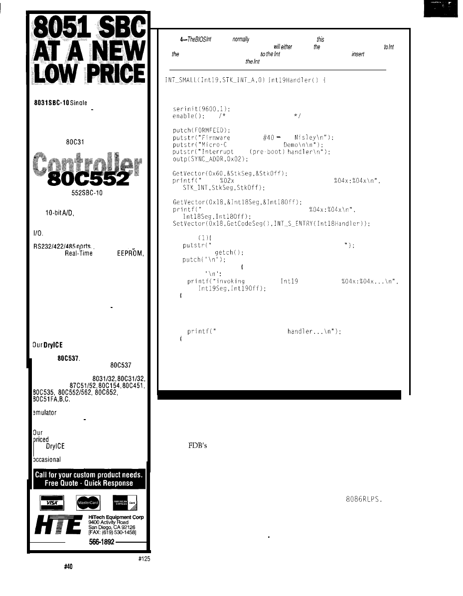
We are proud to offer our standard
Board Comouter
at a new, low price just $79 pei unit
or as low as $49 each for quantity pur-
chases. An 8031 with two JEDEC
sockets, one RS232, 5V regulator,
expansion connector. Optional second
serial port,
or 32.
At $149, our
has the price
and features you need right now! It’s an
8051 core processor with an eight chan-
nel,
two PWM outputs, cap-
ture/compare registers, one RS232, four
JEDEC memory sockets, and more digital
And we didn’t stop there! You can
add
options
like’
two
more
24 more dioital
I/O ports,
Clock,
and battery-backup for clock and RAM
right on board. Start with the Develop-
ment board; it has all the peripherals
plus a debug monitor for only $349.
Download and debug your code -right on
the SBC. then move to the OEM board
above fdr your production needs. We
also do custom design work call for our
reasonable prices.
New 8051 Family
Emulator Support
P l u s p r o d u c t h a s b e e n
expanded to include support for the
Siemens
The base emulation unit
IS
still only $299, with the
pod
priced at $199. Other 8051 family proces-
sors supported are
3 7 5 1 1 5 2 ,
a n d
Each of these pods is
priced at $149. Where else can you get an
with this much power and flexi-
bility for only $448 complete?
original stand-alone 8031 ICE is still
at
$199.
Though not as flexible as
the
Plus, it offers excellent
price/performance for learning or the
job need.
(619)
Listing
19 handler
boots a program from
disk, buf handler gives you a choice.
Depending on the serial input character if
boot using B/OS handler (which was moved 61
by startup code) or pass control directly 18 boot failure handler. You can
an entire
application program either here or in
18 handler!
int Option:
allow timer ticks
Furnace
Ed
BIOS Extension
19
Int
pointer to top of stack is
Capturing Int 18 vector, was
while
Press Enter to boot or Esc to skip:
Option =
switch (Option)
case
previous
handler at
asm
INT $61
break:
case ESC:
invoking our Int18
asm
INT $18
break:
replace, modify, or extend standard
module
8086RLXS. ASM.
You can
BIOS services. For example, you could
modify
BIOSEXT. LIB
toinclude
redirect the BIOS Int 10 video routines
specialized library files or exclude
to use the
character LCD
Micro-C library files as needed.
panel.. .it may be a mite cramped, but
The Micro-C CC86 Command
your applications could use a video
Coordinator has no way to specify a
display or the LCD with no changes.
Get the picture?
RELEASE NOTES
Because BIOS extensions require a
modified startup routine that isn’t
useful for normal C code, I created a
separate library file called B I 0 S E XT
L I B
that includes the startup code
library other than TINY or SMALL, so
I’ve been using my
MCCOMP
batch file
to create the extensions. You can
simply replace the
ASM
file
with (renamed) 8086RLXS.
ASM
and
use Small model if that is more
convenient.
The code on the BBS includes the
source files, the demo code,
MC C OM P,
54
Issue
November 1993
The Computer Applications Journal
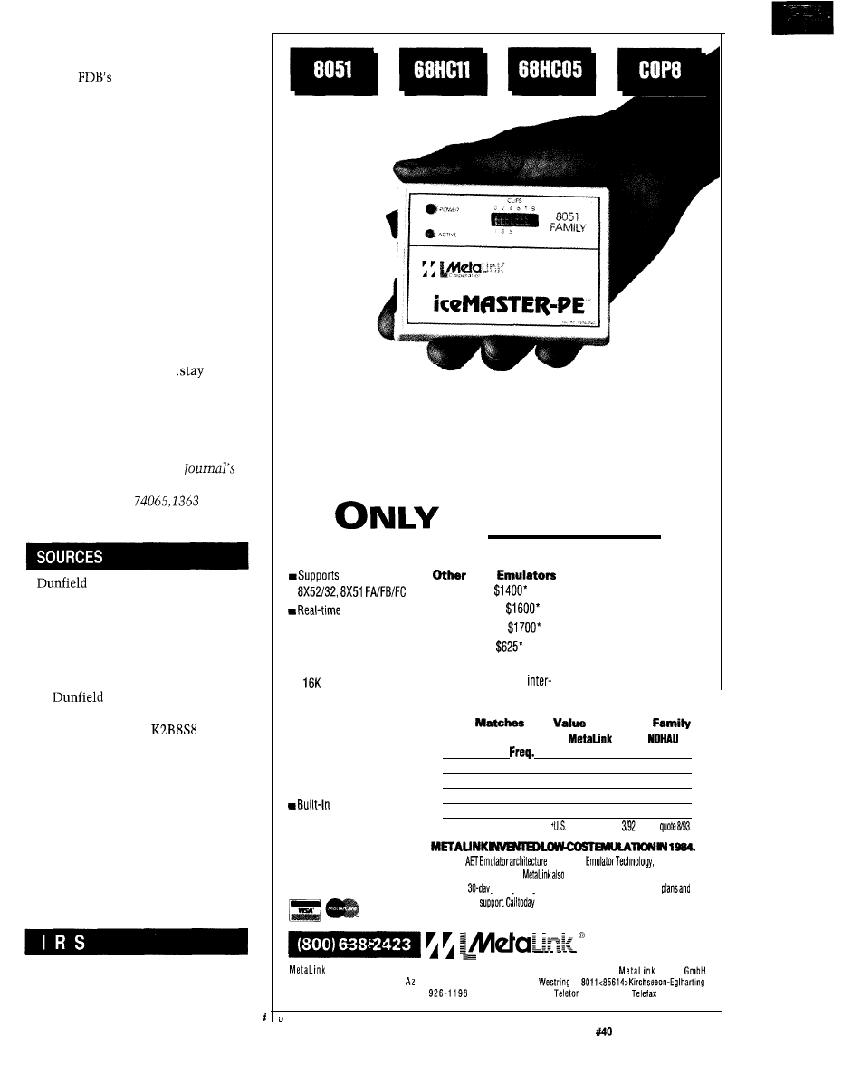
and the extension boot loader. You’ll
need the
battery-backed RAM
and write-protection circuitry to make
use of the loader, although you can use
EEPROM with an emulator instead.
I still think 32K bytes isn’t enough
room for a complete PC program, but
this month’s sample code should
provide a framework for building BIOS
extensions and diskless programs. Just
don’t get carried away and smash into
that 32K limit halfway through a
project!
Next month I plan to explore
Paradigm’s LOCATE and TDREM
programs. Although Micro-C is a great
cost-performer, I know many of you
have been eager to use your Borland or
Microsoft compilers with the Firm-
ware Development Board..
synched!
q
Ed Nisley, as Nisley Micro Engineer-
ing, makes small computers do
amazing things. He’s also a member of
the Computer Applications
engineering staff.
YOU
may reach him
on CompuServe at
or
through the Circuit Cellar BBS.
Development Services has
just released Micro-C 3.0, which
includes structures and unions as
well as a “DOS-less Utilities
Diskette” that automates some of
the hocus-pocus I’ve described
here. Contact:
Development Services
P.O. Box 31044
Nepean, Ontario
Canada
(613) 256-5820
Fax: (613) 256-5821
Pure Unobtainium has the com-
plete Firmware Development Board
schematic, as well as selected parts.
Write for a catalog:
13109 Old Creedmoor Rd.
Raleigh, NC 27613
Phone/fax: (919) 676-4525
410 Very Useful
411 Moderately Useful
412 Not Useful
T
HE
I
N C R E D I B L E
N
E W
PE-835
1
FX
I
N
- C
IRCUIT
E
M U L A T O R
$1451.00
8X51/31,
Fine
New Debugger
n
8051 From
Enhancement8
and Nonintrusive
n
68HCll From
n
Full support for structures,
n
64K Program Memory
n
68HC05 From
unions, arrays, pointers
64K Data Memory
n
COP8 From
n
Data structure
n
l28K Hardware Breakpoints
n
More than 100 devices
browser/editor
n
Frame Trace Buffer
supported through
n
True expression in watch
window-detect bad pointers
n
Transparent Trace
changeable probe cards
(View Trace and Execute
Nobody
the
of the PE
Simultaneously)
PE Product
Max
n
Fast, Easy Installation to
list Price*
List Price*+
RS232 Port of any D
OS
P C ,
8351 FX
1 6
$ 1 4 5 1
$4820
even Laptops!
8 3 7 5 1 1 7 5 2 1 6
8 5 1
4300
Self-Test
8032-24 24
8 5 1
4945
8032-42 42
999
7 1 9 5
n
Symbolic Debug
*U.S. Retail price.
Price
List dated verbal
n
Source-Level Debug
Our new
(Advanced
Pat. Pending)
provides unmatched value.
delivers leading edge
customer service,
including a
money back guarantee, 10 dav trial periods, rental
free technical
for FREE
demo
diskette.
C o r p o r a t i o n - - -
Corporation
Europe
325 E. Elliot Road, Chandler, 8 5 2 ’ 2 5
2,
Phone: (602) 926-0797 Fax: (602)
(08091) 2046,
(08091) 2386
The Computer Applications Journal
Issue
November 1993
5 5
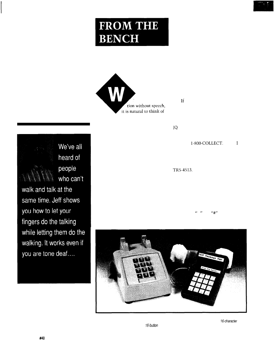
Talk on the
Phone
Without a
Word
Jeff Bachiochi
hen we visual-
ize communica-
the hearing and speech impaired who
use signing. But sign language is used
by many wherever aural communica-
tion is impractical.
The steel worker directs the
placement of mammoth girders by the
simplest of hand movements. His
distance from the crane operator
requires the use of signing to commu-
nicate.
Giant aircraft are shoehorned into
crowded terminals with the aid of sign
language. Our vocal cords are no
match for engine noise and sealed
cockpits.
A scuba diver must communicate
by gesture because there is something
else stuffed in his mouth that gets in
the way of talking..
The old saying “a picture is worth
a thousand words” may be true in
many situations, but in other situa-
tions, a word or two will do fine thank
you very much. Last month, I intro-
duced the new telephone interface for
the HCS II. Adding the speech synthe-
sizer option gives your HCS a voice.
This comes in handy if you wish a
report on your home’s status over the
phone. But what if you don’t have the
voice output option? Most of us can’t
interpret DTMF tones directly, but
what if we could?
BEEP ONCE FOR YES,
TWICE FOR NO
only we could make sense out of
those tones. Take a look at your
phone’s keypad. Notice that in
addition to the numerals, the buttons
labeled 2-9 also have letters on them
and W are missing, though). Today,
these alpha characters replace numer-
als as in the latest ad campaign, for
instance:
When
was younger, our town’s exchange
was identified by a two-letter prefix to
our five-digit local number. So, our
phone number was something like
The “TR” stood for
“TRemont’‘-the exchange’s ID-and
the digits “87.”
Although these alpha characters
can represent digits, it is a bit more
tricky to make digits identify charac-
ters. After all, each digit could be any
one of three possibilities. If we can
assume the * and
will not be
used to represent themselves, we can
reassign their use for “alpha pointing.”
Photo l--The Message Man interfaces with
the telephone through the handset. A microphone and speaker are held
onto the handset with strips of Velcro. The self-contained unit displays messages on a single-line
LCD
display while it accepts user input on a
keypad.
56
issue
November 1993
The Computer Applications Journal
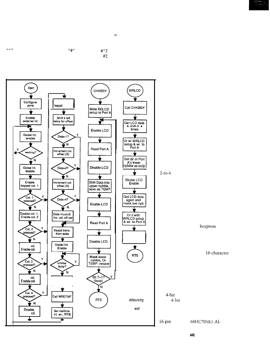
That is, any digit preceded by one or
both of these characters represents not
the digit, but one of that digit’s
characters. The actual character is
based on the pointer.
One possible scenario might be a
points to the left character, a
points to the right character, and when
both of them arrive together they point
to the center character. For example,
the following meanings could be
decoded from these sequences based
on the “2” button:
2
2
l
2 = A
l
#2 = B
= B
= c
This method does require up to
three tones per character, but it opens
Disable
2.
3
Disable
3.
4
keypad
4
Disable
Set F.
Global int
U
disable
Shift Data into
upper nybble,
save as TEMP
as
Strobe LCD
Enable
Figure l--This month’s
software uses two interrupt
routines
for
and
for tone defection and
transmission, as
as a
main loop that scans for a
keypress.
up a whole new approach in communi-
cations, that is, with the help of this
month’s project.
I’M ALL EARS
With a bit of computing power, we
can decode those blipity-bleeps into
real messages and display them on a
single-line LCD. For those times when
you may run into one of the last of a
dying breed-the rotary phone-a
keypad and DTMF encoder can be
added. The encoder provides access to
all sixteen DTMF tones, which you
may find adds a bit of security.
Remember, the typical Touch-Tone
phone only has twelve buttons and, as
such, twelve tone combinations.
The system consists of a keypad,
an LCD display, a DTMF encoder/
decoder, and a microcontroller.
Priority is given to the DTMF decoder
to ensure each decoded tone burst is
read, converted, and displayed prior to
the receipt of the next tone.
While a keypad decoder would
have eased the software burden, I
wanted to keep the parts cost to an
absolute minimum. So, I used a simple
line decoder as a keypad row
driver (actually, I used a ‘238 instead of
half of a ‘239). The rows are sequen-
tially enabled by the processor while
the columns are sampled for switch
closures. A switch closure is detected
when data other than zero is read. The
ideal chip here would have been a
tristate device, but since the ‘238 is
not,
I
added diodes to the column
lines. This prevents a
(which
connects the ‘238’s outputs directly to
the data bus) from interfering with
other operations during the times
when the ‘238 is disabled.
I chose a single-line,
LCD display for its small size and
availability. I got this one for less than
$10 from Timeline. It even came with
EL backlighting (minus the inverter).
The MT8888 DTMF decoder uses a
nybble-wide data bus, as would the
keypad’s columns, so using the LCD in
the
mode seemed appropriate.
A
data bus reduced the
number of signals necessary to 10 plus
an interrupt. I wanted to avoid exter-
nal RAM and ROM, so I turned to the
Motorola
The Computer Applications Journal
Issue
November 1993
57
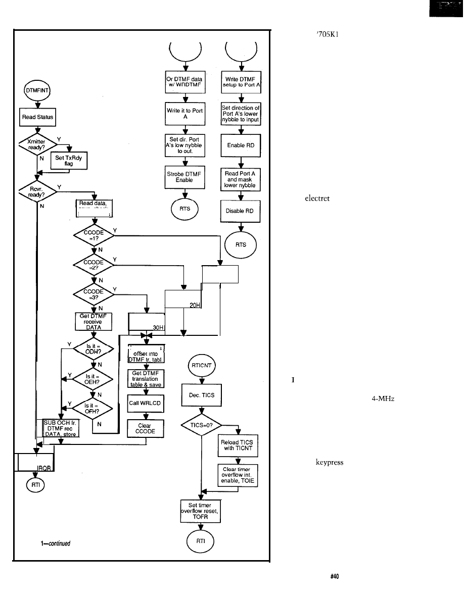
n
n
WRDTMF
RDDTMF
Read Status
save, check
kevor. codes
RTS
Get DTMF
rec. DATA,
ADD off. 1 OH
Get DTMF
rec. DATA,
ADD off.
Get DTMF
rec. DATA,
ADD off.
Put into X as
. . .
Figure
Set interrupt
request
reset.
though the
is not new technol-
ogy (really just an ‘05 core), it com-
petes pin for pin with the same size
PIC processor on price, power, and
speed.
ANALOG CONNECTION
To
make this project universal and
portable, and to avoid the expense of a
registered DAA (data access arrange-
ment), I made the audio connections
through the phone’s handset. This
eliminates direct connection hassles,
but does require you to attach a mic
and speaker to the handset during
communications. I used Velcro strips
to hold these on the handset like a
blood pressure cuff around your arm. I
used an
microphone to listen
to the DTMF tones because it needs
minimum amplification to reach the
maximum signal input to the DTMP
decoder (1 volt]. The encoder output
will not directly drive a speaker, so I
used an LM38.6 amplifier to get the
necessary power.
Because the phone is designed to
allow you to hear your side of the
conversation as well as your
counterpart’s, any button you press
that is encoded into a transmitted
DTMF tone will be received, decoded,
and displayed on the LCD as well. I’m
not sure whether to call it a benefit or
a shortfall, so let’s label it a feature. In
fact, it allows the unit to self test.
SOFTWARE OVERVIEW
used two interrupt routines in
this month’s project. The first is a real-
time interrupt. When using a
crystal on this processor, an RTI can
be produced every 33 ms. The RTI
routine controls a delay period which
debounces the switches and prevents
the unit from producing multiple
DTMF tones. The RTI is enabled
whenever a
is detected and
disabled immediately after the timeout
period.
The second interrupt is an
external interrupt from the DTMF
encoder/decoder. It signifies a tone has
been sent or received. If the status
register indicates a tone has been sent,
a software flag is set to indicate the
transmitter is empty. If the status
register indicates a DTMF tone has
The Computer Applications Journal
Issue
November 1993
59
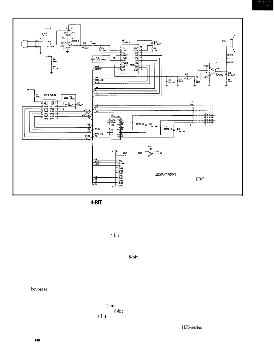
Figure 2-Hardware
is kept to a minimum by using an
processor and
doing most functions in
software. The one exception is
transmitting and
receiving, which is done using the MT6888 transceiver chip.
been received, the processor reads the
DTMF receive register. The data
corresponding to the decoded tone pair
received is translated into a printable
character through a lookup table and
sent to the display.
The main loop scans for a
keypress. This process is bus intensive
and often holds the bus active. If
interrupted during a scan, the chances
of data being passed successfully are
nil (since an active-high output on the
‘238 will be passed on to the data bus).
Therefore, interrupts are globally
disabled during these activities.
If the real-time interrupt has timed
out and a
is detected, the row
and column data are used to determine
a table offset. This table’s data is sent
to the DTMF encoder which produces
the appropriate tone pair output. Then
it’s back to look for another keypress.
See the flowcharts in Figure 1 for more
detail.
LCD MODE
The LCD display’s 4-bit mode is
not difficult to use, but it can be a bit
confusing. In 4-bit mode, only the
upper 4 bits of data are used, which
means all commands must be sent
using two
transfers. The first
transfer is the upper nybble and the
second is the lower nybble. Simple,
right? Well, mostly. You see, the
display comes up in
mode on
reset. If the first command sent to it is
“use 4-bit mode,” then successive
transfers will be two 4-bit transfers.
But we’ve only got a 4-bit bus, so how
do you send that first command?
This special command uses only
the upper nybble (the lower nybble is
ignored). The first command is sent as
a single
transfer, and is inter-
preted as an
transfer that selects
the
mode. Successive commands
are now done with two 4-bit transfers.
That goes for reading the display
registers as well. Two reads are
necessary to receive a full 8 bits.
One other note about the display
mode used here. I chose to have the
display scroll from the right to left
with new characters showing up on
the right side of the display, pushing
the existing characters one position to
the left. This is similar to a moving
banner style of sign. This differs from
the normal mode in which the cursor
moves from left to right.
PACKAGING
If you have a Touch Tone phone
and don’t need the keypad, DTMF
encoder, and audio source, then this
project will fit into a very small
package. But if you want a 16-button
interface or have only rotary dial
phones, you will want to build the
complete project, which needs a
slightly larger container. I used a
Pactec
enclosure.
6 0
Issue
November 1993
The Computer Applications Journal
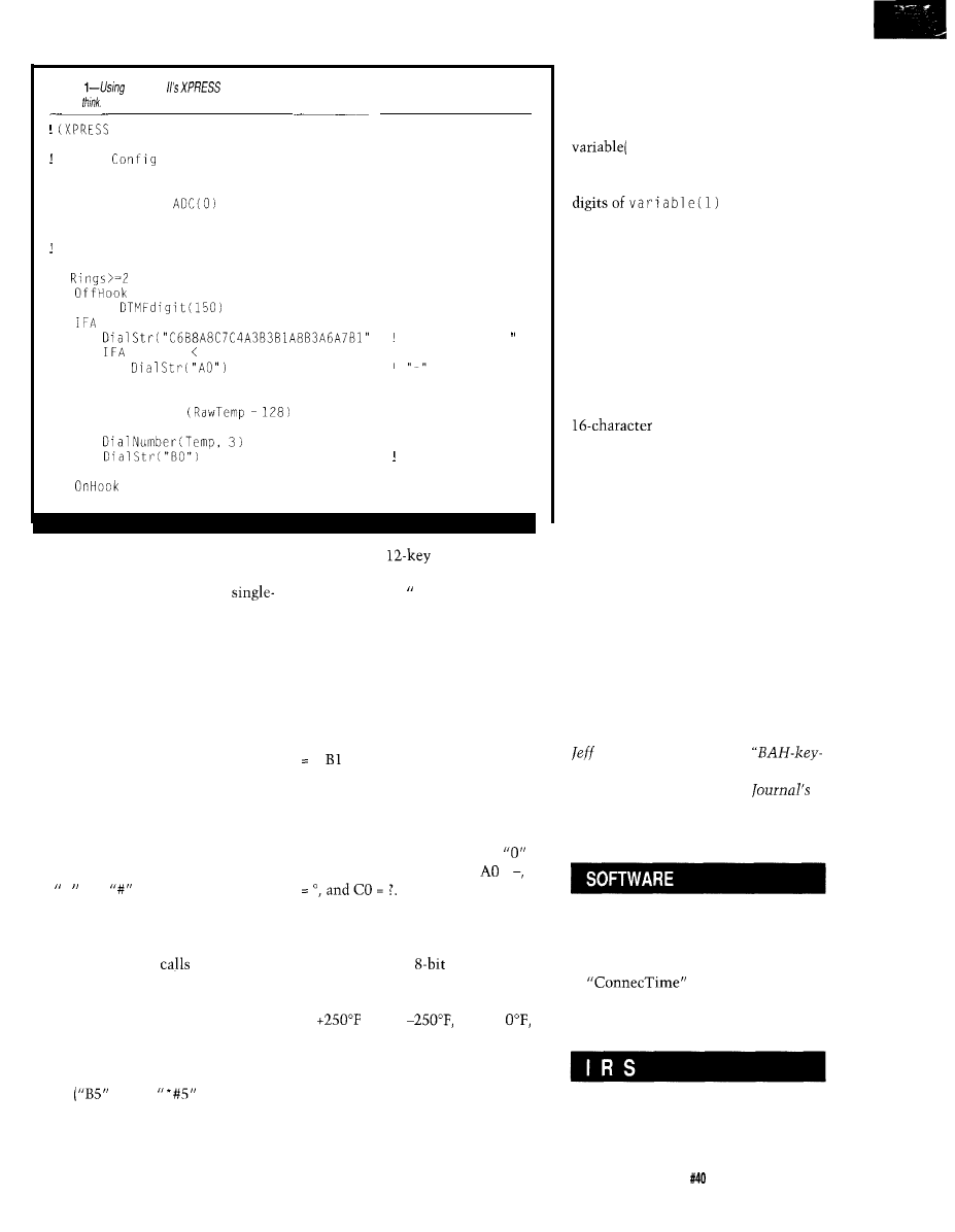
Listing
the HCS
language, conversing with the Message Man is easier
than you
might
syntax)
System
Section
DEFINE Key
= Variable(O)
DEFINE RawTemp =
DEFINE Temp
= Variable(l)
Program Section
IF
THEN
Key =
Key = 15 THEN
RawTemp 128 THEN
Temp = RawTemp * 2
ELSE
! Look for D button
"OUTSIDE TEMP
Temp =
* 2
END
! ADC Reading
Degree symbol
END
END
I made the keypad from discrete
push-button switches mounted on a
separate piece of protoboard. A
row, stick-pin connector mates this
keypad with a second piece of
prototyping material. The circuitry
shown in Figure 2 is mounted on the
second board.
Graphics for the “Message Man”
project cover the LCD display and
keypad portions. I printed these on
paper and glued them to the back side
of translucent mylar to keep the
graphics from being rubbed off.
IMPLEMENTATION
The “Total Phone” service offered
by our local telephone company uses
the
l
and
as special function
keys to indicate call forwarding and
other value-added features. Using
these keys as alpha pointers may
inadvertently cause
to be for-
warded to somewhere else or cause
some other problem. I chose instead to
use three of the additional DTMF
codes (A, B, and C) as alpha pointers.
This improves two things. First, the
maximum character sequence length
is two
versus
to indicate
the character “K”). Second, these
characters cannot be produced using
the standard
Touch Tone
phone, so there is a level of security.
Because the 1” and “0” digits do
not have any alpha characters assigned
to them, the lookup table can assign
any characters you want to them [or
any other key for that matter). Two
alpha characters-Q and Z-are not
included on the digits 2-9, so I’ve
arbitrarily assigned them and the space
character to the “1” key as follows:
Al
Q,
= space, and Cl = Z. I took
advantage of one of the special charac-
ters in the LCD’s character generator
when assigning characters to the “0”
key. This is a small elevated circle
used as a degree indicator. The
key
assignments are as follows:
=
BO
Listing 1 shows what is necessary
to send a typical message from the
HCS indicating the outside tempera-
ture. I assume an
ADC with a
temperature sensor output of O-5 volts
indicating temperatures from -250°F
to
(0 V =
2.5 V =
and 5 V = 250°F).
If the DTMF code for the “D” key
is received by the HCS, then a string of
DTMF codes is sent. This string
represents the characters “OUTSIDE
TEMP.” Next, channel 0 of the ADC is
compared to a constant
(128)
to
determine if the reading is a negative
temperature. If so, the DTMF code
“AO” is sent (the minus sign) and
1) is set to twice the difference
of the reading and the constant. The
next statement sends the last three
(which
contains room for four digits and the
actual temperature reading). Finally,
the string “BO” is sent, which repre-
sents the degree symbol.
At your end of the phone, pressing
the “D” key tells the HCS that you are
ready for a transmission. In turn, the
HCS blurts back tones which are
displayed as “OUTSIDE TEMP 84°F.”
Note that this message has more
characters than can be displayed on a
display. However, the
characters are scrolled in a right-to-left
fashion, which allows even rapidly
scrolled messages to be easily under-
stood thanks to the persistence of
vision.
“...PRESS ONE FOR MORE
OPTIONS...”
Now
it’s your turn to build one of
these and receive that coded status
report from your HCS without it
saying a word. Just don’t let the kids
see this project or you’ll end up
building a pair for them. Then again,
they may have never heard of Dick
Tracy.
q
Bachiochi (pronounced
AH-key”) is an electrical engineer on
the Computer Applications
engineering
staff.
His background
includes product design and manufac-
turing.
Software for this article is avail-
able from the Circuit Cellar BBS
and on Software On Disk for this
issue. Please see the end of
in this issue for
downloading and ordering
information.
413
Very Useful
414 Moderately Useful
415 Not Useful
The Computer Applications Journal
Issue November 1993
61
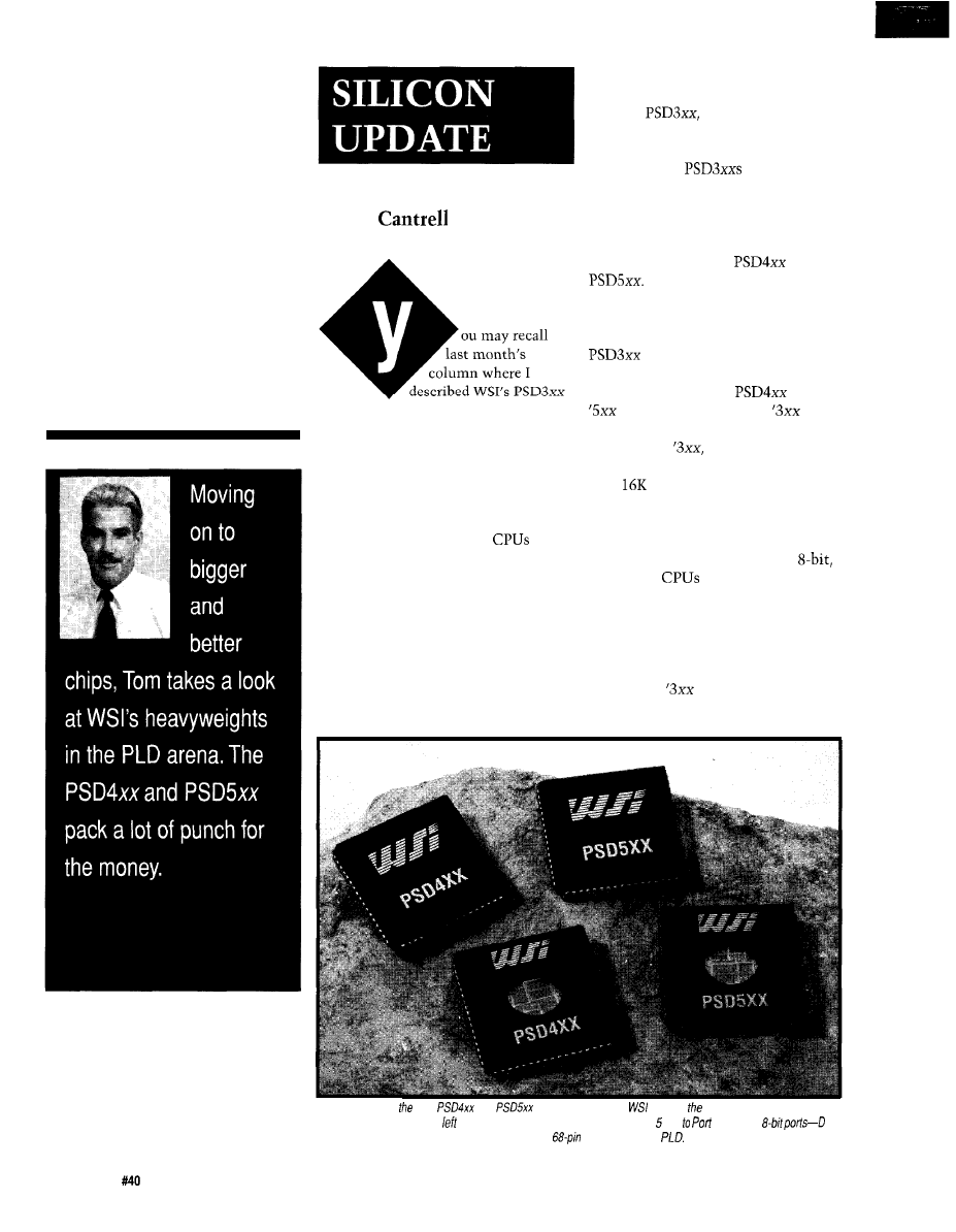
The Swiss
Army Sends
in the
Special
Forces
Tom
family of combo chips which combine
EPROM, RAM, and glue logic into a
single package.
I also described the marketing
theory and constraints behind the
combo-chip concept. Namely, the
niche for such a chip is the window
between where single-chip
top
out and where the brute-force pricing
of commodity chips kicks in. Failure
to stay between the lines spells doom,
as it did for the circa-‘70s first genera-
tion of combo chips.
The key point is that, as technol-
ogy evolves ever onward and upward,
the window moves as well. The harsh
realities of the ever-changing IC
market demand that combo chips
adapt-or die.
The
like your average GI,
does a good job holding ground. It
must, because according to WSI, more
than 1 million
have been
shipped to date. However, with further
attack on the combo chip niche
inevitable, it’s time to send the Special
Forces forward to prepare for the next
assault. Enter the new
and
BE MY PAL
Fortunately, having explained the
in detail last month makes
describing these new parts easier. As
shown in Figure 1, the
and
(Photo
1)
build on their
predecessor.
Like the
the new parts
combine up to one megabit of EPROM
with
bits of SRAM. I’m a little
surprised that WSI didn’t take the
opportunity to offer versions of the
new chips with more memory than
before. After all, some high-end,
single-chip
are starting to
encroach on entry-level PSD memory
density (i.e., 256K bits EPROM). On
the other hand, adding memory will be
easy-thanks to the on-board bank
selection logic-when the need arises.
As with the
family, versions of
the new chips are offered that support
Photo l--A/though new
and
series of chips from
present same amount of memory,
EPROM access times have their predecessors far behind. An additional bifs
C and two
and E-have made these chips info a more powerful
genera/-purpose
62
Issue
November 1993
The Computer Applications Journal
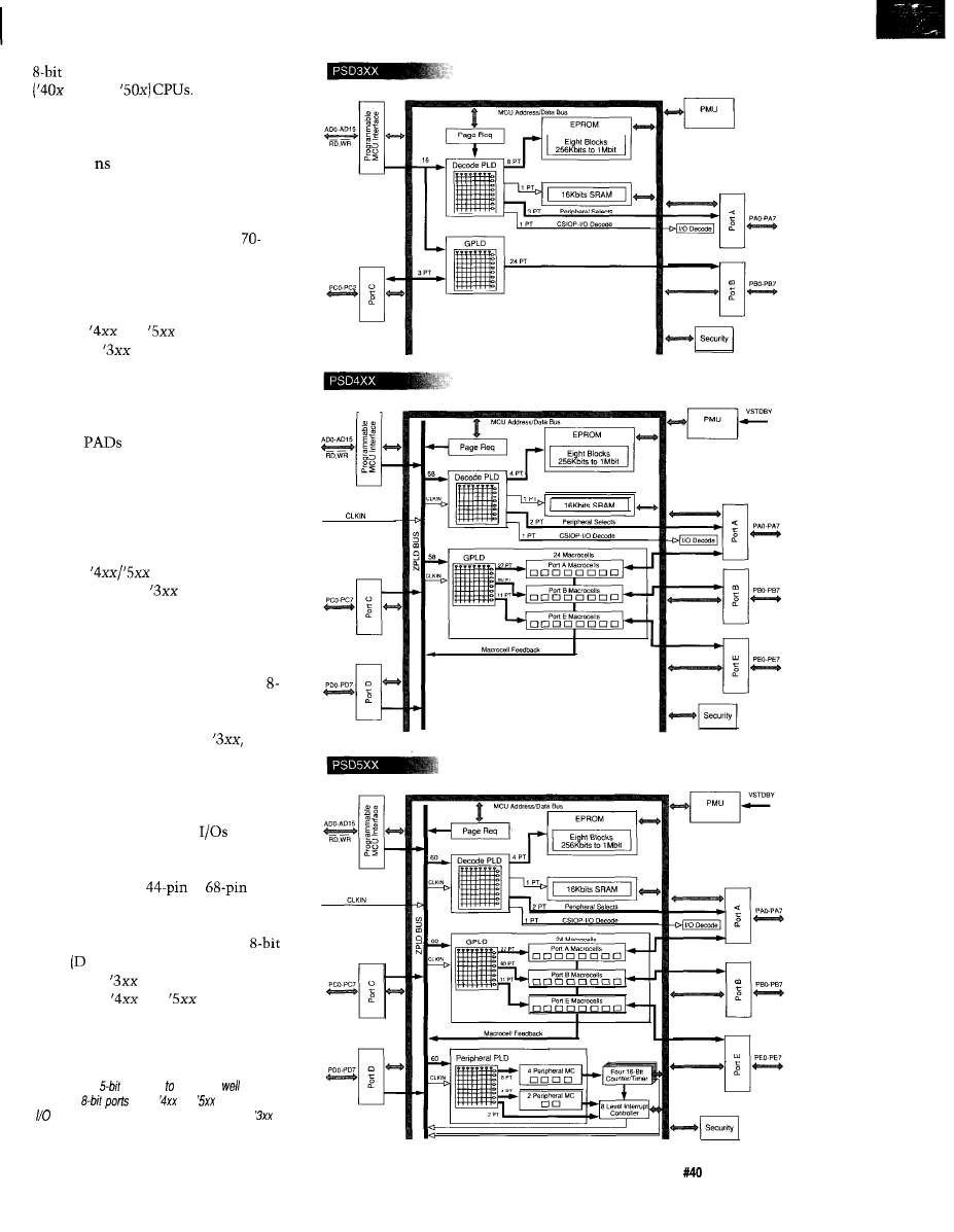
(‘41x and the ‘51x) and 16-bit
and the
Though there isn’t more memory,
what’s there is much faster than
before, with EPROM access times as
fast as 90 available. Remember, the
PSD access time includes the on-chip
decode and MCU interface delay.
Thus, an equivalent multichip solu-
tion would require a faster-say
ns-EPROM to make up for the
slowdown imposed by external buffers
and decoders.
The major addition common to
both the
and
was hinted at in
the earlier
parts. You’ll remember
that a few pins (3 bits of Port C) were
available for optional general-purpose
use (versus typical use as address
inputs or chip select outputs) with the
on-chip
(Programmable Address
Decoders).
Note that what were formerly
PAD A and PAD B have now been
more clearly named “DPLD” (Decode
PLD) and “GPLD” (General-purpose
PLD).
The
DPLD is little
changed from the
PAD A and still
serves mainly to map accesses to the
EPROM blocks, SRAM, and other
internal resources. Indeed, the number
of product terms is reduced from 13 to
8, largely due to the switch from an
bank to a 4-bank EPROM scheme.
Anyway, the general-purpose PLD
functionality offered in the
while
interesting, probably wasn’t enough to
be of great value in most applications.
I imagine WSI was deluged with
customers demanding they beef it up.
Since a PLD without
is about
as useful as a write-only memory, the
first big change with the new parts is
the move from a
to
leaded (plastic or ceramic, windowed
or OTP) chip carrier. Adding five more
bits to Port C and two additional
ports and E) boosts, I/O from the 19
lines of the
family to a healthy 40
lines in the
and
families.
n
Figure l--The
increase port C as
as two
additional
to the
and
families means
lines have extended from 19 (existing on the
family) to 40 lines.
The Computer Applications Journal
Issue
November 1993
6 3
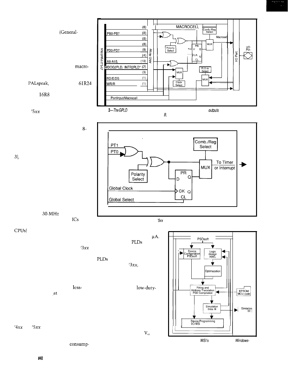
Having established supply lines,
the command post takes the form of
a very powerful GPLD
purpose PLD). The GPLD offers up to
61
inputs including all 40 port pins
plus a variety of MCU bus and internal
control signals. One hundred eighteen
product term outputs feed three
separate groups of 8-registered
cells (Figure 2) connected to Ports A, B,
and E.
In
the GPLD is a
-which is nothing to sneeze at given
that a lowly
costs a buck or so.
SYNCHRONIZE YOUR WATCHES
The
ups the ante even further
by adding yet another PLD-the Pe-
ripheral PLD or “PPLD’‘-intertwined
with a 4x16-bit timer/counter and
level prioritized interrupt controller.
Potential interrupt sources include
two from the PPLD AND/OR array,
two from its macrocell outputs (Figure
and terminal count indicators from
four on-board timers. Similarly
routable, the interrupt controller’s
outputs can be directed internally to
the DPLD and PPLD or via Port E to
the CPU.
The clock sources for the timers
can be programatically defined as
inputs from Port E, outputs of the
PPLD, or a new CLKIN pin. The latter
features up to
input (that’s
much faster than most timer
or
timer subsystems on single-chip
and a programmable divide
ratio from x4 to x280.
The timers play a role in improved
power management. The original
did have a chip select input that would
totally shut down the device to
conserve power. Unfortunately, this
posed the classic chicken and egg
dilemma-how to power up the PSD
given that the software for the CPU to
do so resides in the PSD! The
than-ideal solution the time called
for external logic to detect the CPU’s
first stirrings and splash cold water on
the PSD in time for it to deliver the
first morning cup of hot opcodes.
Now, thanks to the timers, the
and
can be put in a mode
where everything except the I/O ports
is shut down automatically after 15
clocks. At this point, power
PAO-PA7
GPLD
PEO-PE7
Output
PCO-PC7
P G R O - P G R 3
AO, Al
CSI, CLKIN, Reset
W
Reset
CLKIN
Feedback
Figure
offers up to
61
inputs. One hundred eighteen product term
feed three separate groups
of b-registered macrocells connected to Ports A, and E.
PPLD Macrocell
Figure
3-Potential interrupt sources on the
series include two from the PPLD AND/OR array, two from ifs
macrocell outputs (shown here), and terminal count indicators from the four on-board timers.
tion dwindles to a measly 2
Furthermore, the
offer the
so-called “zero power” feature in
which edge detectors power the
down when the inputs are
static. As in the
a configu-
ration bit can specify that the
EPROM be powered down
when not selected, reducing
power (especially in
cycle applications) at the expense
of slightly lengthened access
time.
Another addition on the
low-power front is the addition
of a new VSTDBY pin which
provides dedicated power to the
SRAM array. Whenever
falls
more than 0.7 V below VSTDBY,
the SRAM is automatically
MS-Windows
Logic
ABEL
Data
Magic Pro -Other
EPROM
MCU code
SILOS
Figure
4-Software for
PSD family is now
based and includes Data I/O’s ABEL.
64
Issue November 1993
The
Computer Applications Journal
switched into backup mode, consum-
ing minimum power and protected
from glitches.
DUELING BUSES
Before we can contemplate the
entire spectrum of possibilities posed
by the new
there is one more
feature to consider. As shown in the
various block diagrams, there are
actually two buses on board-the
MCU bus (i.e., the typical address,
data, and control lines) and the
ZPLD bus connecting the D-, G-, and
Note that most resources (such as
the ports, timers, etc.) connect to both
buses, effectively allowing them to be
bridged when it makes sense. How-
ever, the appropriate splitting of effort
between the buses offers the potential
for more optimal designs.
In particular, the ability of the
(and timers and the interrupt
controller in the
to communicate
privately allows significant processing
to be performed in hardware without
host CPU intervention.
Such a setup is ideal for handling a
variety of low-level functions such as
encoders, decoders, waveform genera-
tors, shift registers, BCD counters, and
on and on. Benefits include freeing up
of MCU bandwidth and interrupts
and/or eliminating the need for
external chips.
PSD DIVIDEND
Perhaps more than the chips, the
software development tool has been
radically changed from that offered for
the original
With little general-
purpose PLD functionality, the
based MAPLE
software was
organized as a kind of fill-in-the-blanks
exercise, selecting from a set of
predefined functions and options.
The new
(Figure
besides running under Windows
instead of DOS, deals with the general-
purpose PLD capabilities of the new
parts by incorporating Data I/O’s
ABEL. Going even further, a Verilog
HDL (Hardware Description Language,
i.e., C for chipheads) description of the
PSD can be simulated with Simucad’s
SILOS III. Indeed, the Verilog model
can be plugged into higher-level board
is
C thru ROM?
ROM
Borland
or
is the
complete ROM development software tool kii.
lets you run
Microsoft and Borland C and C++ programs on an
embedded
CPU without using DO6 or a BIOS.
saves you
money.
no DOS or BIOS royalties
to pay for your embedded systems.
is complete! It includes the following and much more:
*Supports Borland’s Turbo Debugger.
*Remote Code View style source level debugger.
l
ROMable
code brings CPU up from cold boot,
l
ROMable library in
source code.
*Flexible
Locator.
PACKAGE
$495.
MONEY
GUARANTEE.
real
mode
family
80386
protected mode
R3000,
Features
l
Full-featured, compact
l
Supports inexpensive PC-hosted
kernel with fast interrupt response
development tools
l
Preemptive, priority based task
l
Comprehensive, crystal clear
scheduler with optional titne slicing
l
Mailbox, semaphore, resource,
l
No-hidden-charges site license
event, list, buffer and memory
l
Source code included
l
Insight”’ Debug Tool is available
l
Reliability field-proven since 1980
to view systetn internals and
gather task execution statistics
a
Demo Disk and your
l
Configuration Builder utility
Phone: (604) 734-2796
eases system construction
Fax: (604) 734-8114
Count on KADAK.
Setting
real-time
since
1978.
The Computer Applications Journal
Issue
November 1993
65
Multi-Axis
DCX-AT
to 8 Axis Motor/Motion Controllers
l
incorporate state-of-the-art DSP, RISC; and FPGA technologies to
maximum performance at minimum cost
l
DCX controllers provide many sophisticated ON-BOARD control features such a MULTI-
TASKING (the ability to perform independent tasks simultaneously), COMPLEX-CONTOURING,
and the ability to programmed directly in USER-UNITS such as inches, meters, etc.
l
can operate totally STAND-ALONE, using their own on-board “computing +
memory + I/O” capabilities, or EMBEDDED a
They can also be installed in an
ISA-bus (PC/XT/AT), or in a VME-bus
l
DCXcontrollers have a MODULAR ARCHITECTURE for creating a limitless variety of
Application Specific MULTI-AXIS controllers. They are created, in minutes, by installing one or
more intelligent DCX
function modules on an
intelligent DCX
motherboard
l
are supplied
(free) EASY-TO-USE, POWERFUL SOFTWARE for set-
up, programming and operating. These include all major HLL interface programs, with
examples and source code, a CNC control user-interface with G-code and HPGL capability, and
an interactive Servo-Tuning utility
Precision
C 0 R P 0 R A T 0 N
8122
Engineer Rd.
l
San Diego, CA 92111
FAX
AvCase II 8051
and
680x0 Will Travel
Work in the field using your laptop with
AvCase II,
Cactus Logic’s
IDS debugger and
parallel port EPROM programmer.
AvCase II
includes an ANSI C compiler, macro assembler, linker,
run-time and floating-point libraries with source code, librarian,
plus remote monitor and simulator debuggers.
l
Integrates all your tools
l
Manages the edit/compile/assemble/debug loop
l
Compatible with IEEE695
l
Project management, MAKE, on-line help
l
Add your favorite editor, ICE and EPROM
AvCase II 8051
l
Supports derivatives from Intel, Philips and Siemens
l
New global optimizer produces fast, tight code
l
New high-level simulator debugger
AvCase II 680x0 Supports
and CPU300
Save $200 on
II until 1
List Price: $1795 Your cost $1595
120 Union Street, P.O. Box 490
Rockport, Maine 04856
USA
SYSTEMS: INC.
800-448-8500
Fax 207-236-6713
Software Development Tools for Embedded Systems
or system models for complete
application simulation (don’t try
your ‘286, though). The price for
it on
is $1,495, which isn’t as much
as it sounds considering it includes
ABEL, SILOS III, and the Windows
equivalent of MAPLE. Bargain hunters
can get a version of
without
SILOS III for only $695.
Ultimately, as always, the output
of all these software machinations is a
hex file which can be burned into the
PSD with
programmer or some
third-party ones, though it may take a
while for new
adapters to hit
the street.
As for pricing, the temptation is to
add all the prices of an equivalent
multichip setup and tout system cost
savings of reduced chip count as the
reason to switch. Unfortunately, as
more and more features get integrated,
the likelihood that a user doesn’t
need-and thus places no value
some of the chip’s features may
increase.
Just introduced, WSI has an-
nounced that the
series will start
at $6.68 and the
series at $9.81 in
production
quantities. In
my opinion, this pricing is fair given
the amount (and speed of] stuff
included. Go add it up yourself-fast
EPROM and SRAM, high-speed
timers, an interrupt control-
ler,
switching, and so forth.
I think you’ll agree.
q
Tom Cantrell has been an engineer in
Silicon Valley for more than ten years
working on chip, board, and systems
design and marketing. He can be
reached at (510)
or by fax
Integration, Inc.
47280 Kato Rd.
Fremont, CA 94538
(510)
Fax: (510) 657-5916
416
Very Useful
417 Moderately Useful
418 Not Useful
66
The Computer Applications Journal
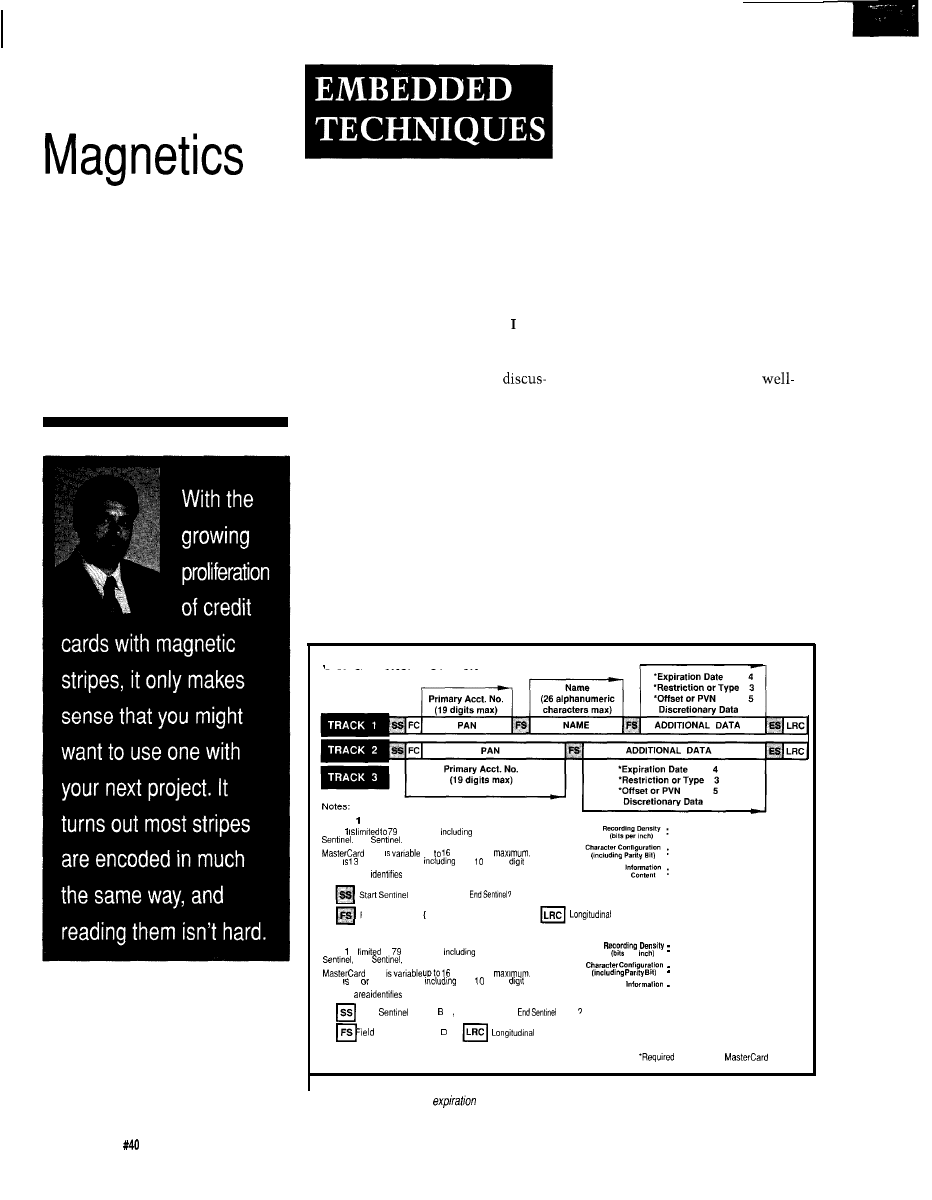
Decoding
that has been served well by technolo-
gies such as Wiegand wire, bar code,
and magnetic cards thus far.
Magnetic media has been used
over the years for data storage in such
applications as core memories, tape,
John Dybowski
and disks. Magnetic cards, such as
credit cards, should be considered a
form of memory exhibiting attributes
like those of touch memories. In this
sion of Dallas Semiconductors’ touch
memory devices. They are an example
of a special type of memory whose
utility goes beyond data storage. Pos-
sessing the functionality of read-only
or read/write-type memories, they
0
cross over into the realm of automatic
identification. Automatic identifica-
tion or data entry addresses concerns
such as material and labor tracking, ac-
cess control, and time and attendance.
ast month
wrapped up my
dissertation on small
memories with a
These touch memories are the
new guys on the block in an industry
defined standards that describe the
physical and magnetic characteristics
for a magnetic stripe on a plastic card.
These standards outline specifications
for a storage format and information
interchange. This does not preclude
regard, this medium not only has the
other encoding techniques or addi-
tional data tracks for specific applica-
capability of read-only storage, but
shares the touch memory’s read/write
tions, but in most cases it makes sense
to adhere to at least the basic con-
attributes. ..with the right equipment.
straints. This gives you the choice of
using any commercially available
magnetic encoders in your application.
MAGNETIC CARDS
Because of their widespread use,
most magnetic cards adhere to
Card Data Format
TRACK
Track
characters
Start
End
and LRC.
PAN
up characters
VISA or 16 characters.
mod check
Shaded area
control characters
%
q
q
Format Code
Field Separator
Redundancy Check character
TRACK 2
Track is
to characters
Start
End
and LRC
per
PAN
characters
VISA 13 16 characters,
mod check
Shaded
control characters
c o n t e n t
ss start
Hex
q
Hex F
FS
Separator Hex =
Redundancy Checkcharacter
by VISA and
lure
l--Most credit card magnetic stripes are formatted in the same way and include information such as primary
account number, name, and
date
68
issue
November 1993
The Computer Applications Journal
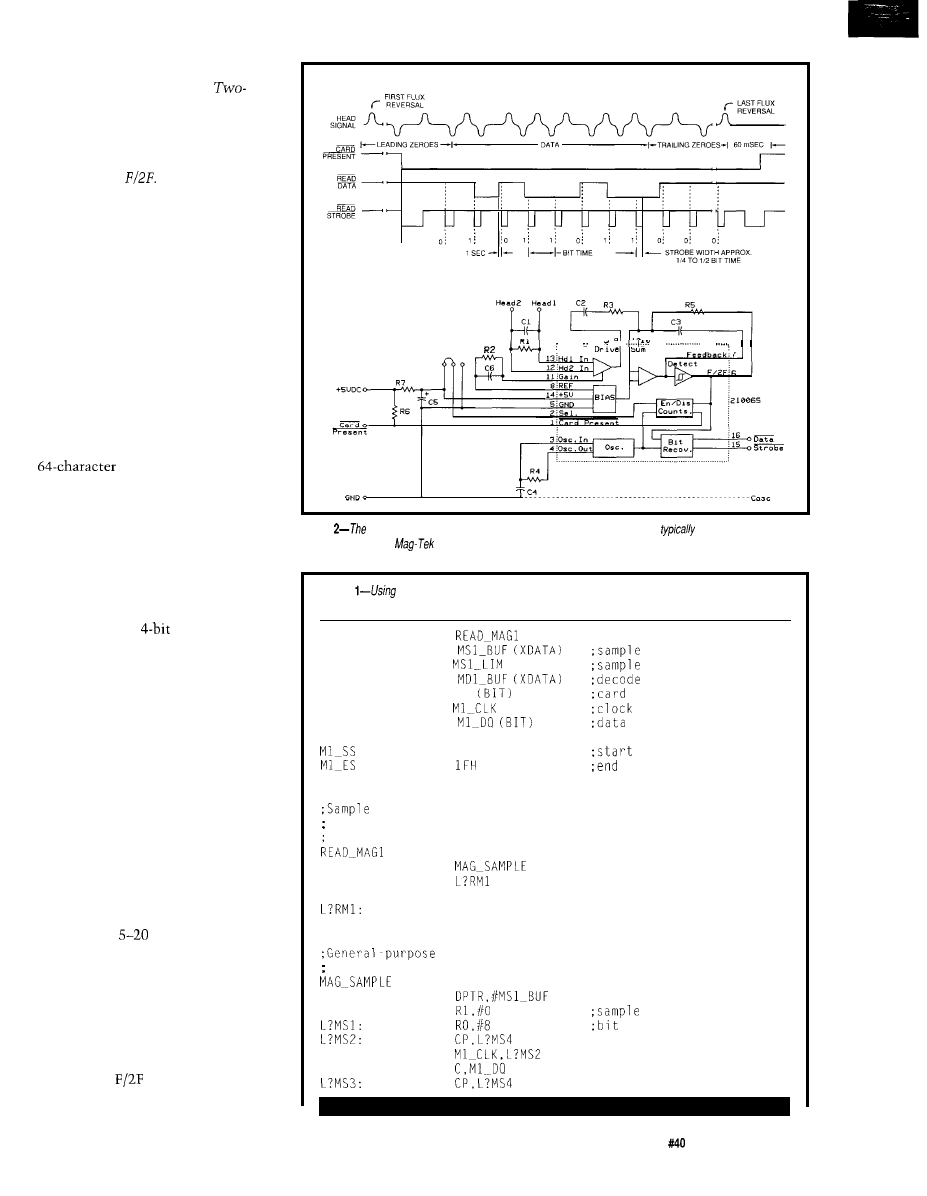
The technique used for encoding
magnetic cards is known as
Frequency, Coherent Phase Recording.
Allowing for the representation of
single-channel, self-clocking serial
data, this methodology is generally
referred to as
Self-clocking is
achieved by combining data and clock
bits together in a continuous, synchro-
nous sequence. In this scheme, an
intermediate flux transition signifies a
one bit and the absence of an interme-
diate flux transition denotes a zero bit.
Three data tracks defined for use
on standard magnetic cards each
possess different bit densities and
encoded character sets. The average bit
density of track 1 is 210 bits per inch
(bpi). Track 1 characters are made up
of six data bits and an odd parity bit,
encoded with the least-significant bit
first and the parity bit last, yielding a
set. Taking the number of
bits per inch and the number of bits
per character, you can see track 1 has
the capacity to hold 79 characters.
Track 2 has a bit density of 75 bpi,
and track 3 uses 210 bpi. Both of these
tracks allow the representation of a
numeric-only character set. The
characters for tracks 2 and 3 are
encoded using a
binary-coded
decimal subset with odd parity and,
like track
1,
are encoded with the
least-significant bit first and parity bit
last. The lower density of track 2
allows up to 40 numeric characters,
where 107 numerics can be squeezed
onto track 3. The actual number of
usable characters will be fewer since
you also have the Start Sentinel, End
Sentinel, and LRC characters.
Though sometimes magnetic
cards are moved past the read head
mechanically, most applications rely
on manually moving the card, either
through a slotted reader or into an
insertion-type reader. Typically the
swipe rate is
inches per second
(ips), with 50 ips being the fastest most
card readers can handle. Of course,
moving the card by hand will not only
result in varying the absolute card
velocity but, will also introduce
incremental speed changes as the card
accelerates and decelerates past the
pickup. The
scheme is very
forgiving of such speed fluctuations.
Signal Timing
Diagram
Figure
complexities of conditioning the raw signal from the
read
head are
hidden by sing/e-chip
solutions such as the
21006505.
Listing
several externally defined routines, a sample program to read a stripe and store it in a
buffer is very short.
PUBLIC
EXTERN
buffer
EXTERN
(NUMBER)
limit
EXTERN
buffer
EXTERN CP
present bit
EXTERN
(BIT)
bit
EXTERN
bit
EQU 5
EQU
sentinel
sentinel
SEG
CODE
and decode magnetic track 1
output: ACC contains character count.
DPTR points to data buffer
PROC
CALL
JZ
CALL
MAGI-DECODE
RET
ENDPROC
magnetic sampling routine
output: ACC contains sample count
PROC
MOV
MOV
counter
MOV
counter
JB
JB
MOV
JB
(continued)
The Computer Applications Journal
Issue
November 1993
6 9
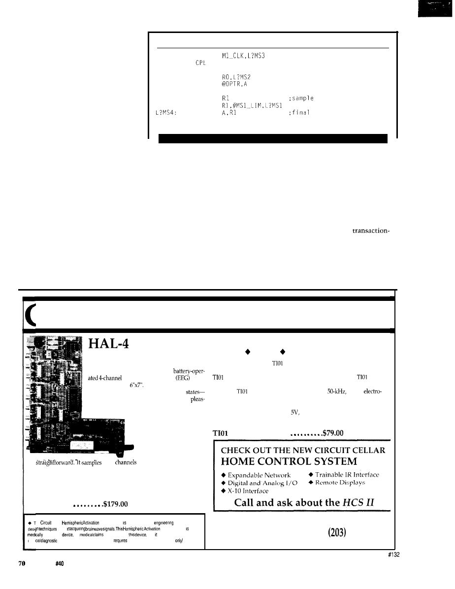
For all three tracks, the fundamen-
tal data format is similar and consists
of the following elements: First, lead-
ing zero bits are encoded to indicate
the presence of an encoded magnetic
card and provide synchronization
pulses to the read head electronics and
ultimately to the controller. Next, the
Start Sentinel character is encoded
which indicates the start of the actual
data. The coded data follows. Next, the
End Sentinel terminates the data por-
tion of the card and followed by an
LRC byte (used for error detection).
The LRC is essentially a horizontal
parity calculated by an exclusive-OR
of all the data bits from the Start Senti-
nel to the End Sentinel (inclusive).
Finally, trailing zeros follow the LRC
and fill out the remainder of the card.
ANATOMY OF A MAGNETIC CARD
The magnetic tracks have inher-
ent characteristics based on details
such as the code set and bit and
character densities. International
organizations such as Mastercard and
VISA impose additional constraints for
their participating members, and
standards exist for bank debit cards
and ATM cards as well. These rules
specify the exact content and format of
each data field in each track as well
the intended uses for the tracks.
Naturally, for nonfinancial uses, it is
not necessary to comply with these
standards. For dedicated uses such as
access control, people tracking, and
material tracking, adhering to the
minimal standards is adequate.
The most-often-used track is track
2, although it offers the lowest
information density of the three. It
Listing l-continued
JNB
c
RRC A
DJNZ
MOVX
INC
DPTR
INC
counter
CJNE
MOV
sample count
RET
ENDPROC
contains all the information that is
normally used for credit card transac-
tions. When a customer name is
required, track
1
must be used since it
the only track that permits alphanu-
meric data. Track 3 is specified for
numeric-only data, but is unique. It is
intended for changeable data and
consequently may not only be read but
may be rewritten by the
handling equipment. A multitude of
data fields are contained in these
various tracks. Figure
1
shows a brief
run-down of what is generally placed
on tracks
1
and 2.
medi
31RCUIT CELLAR KITS
Sonar Ranging Experimenter’s Kit
EEG Biofeedback Brainwave Analyzer
Targeting Ranging Machine Vision
The Circuit Cellar
Ultrasonic Sonar Ranger is based on the
The HAL-4 kit is a complete
sonar ranging circuitry from the Polaroid SX-70 camera system. The
electroencephalograph
which
and the original SX-70 have similar performance but the
Sonar
measures a mere
HAL is sensitive enough
Ranger requires far less support circuitry and interface hardware.
to even distinguish different conscious
The
ranging kit consists of a Polaroid
300-V
between concentrated mental activity and
static transducer and ultrasonic ranging electronics board made by Texas
ant daydreaming. HAL gathers all relevent alpha,
Instruments. Sonar Ranger measures ranges of 1.2 inches to 35 feet, has a
beta, and theta brainwave
TTL output when operated on
and easily connects to a parallel
signals within the range of
printer
port.
4-20 Hz and presents it in a
serial
digitized
format that
Sonar Ranger kit.
plus shipping
can be easily recorded or
analyzed.
HAL’s operation is
‘four
of analog brainwave data 64
times per second and transmits this digitized data serially to a PC at 4800
bps. There, using a Fast Fourier Transform to determine frequency,
amplitude, and phase components, the results are graphically displayed
in real time for each side of the brain.
HAL-4 kit.
plus shipping
he
Cellar
Level detector presented as an
example of the
To order the products shown or to receive a catalog,
used
Level detector not a
approved
no
are made for
and should not be used for
call: (203) 875-2751 or fax:
872-2204
purposes Furthermore, safe use
that HAL be battery operated
Circuit Cellar Kits
l
4 Park Street
l
Suite 12
l
Vernon, CT
06066
Issue
November 1993
The Computer Applications Journal
REALCARDREADERS
The recovery of magnetically
encoded
data can be accom-
plished directly with the use of just
about any microcontroller. There are
no particular difficulties in deciphering
the raw
data stream and many
early magnetic read heads contained
nothing more than signal amplifiers
and line drivers. These are now
artifacts since all modern magnetic
read heads contain integrated
bit
recovery circuitry and interface with
the host controller in a standard
fashion using three wires: card present,
clock, and data. The read heads usually
rely on a single chip to perform the
linear signal conditioning, synchroni-
zation, and recovery of individual bits
from the data stream. The Mag-Tek
21006505 IC is representative of this
type of data recovery circuit and its
functionality is depicted in Figure 2.
Linear conditioning
consists of
raising the level of the magnetic
pickup’s input signal, rejecting
common-mode noise, conditioning and
detecting the signal, and finally
providing a digital output for subse-
quent processing. The enable/disable
counters provide initialization for the
recovery section. The recovery section
locks onto the data rate and recovers
the individual data bits from the data
stream. The oscillator section provides
the clocks for the recovery section and
for the enable/disable timers. Card
present goes low after eight or nine
flux reversals are seen from the
magnetic pickup and will return high
about 50 ms after the last flux reversal.
The strobe line signals that data is
valid and is active low. The Data pin
indicates a one bit when it is low. Raw
data can also be picked directly
the chip. Photo 1 shows a typical
dual-track magnetic pickup and its
associated data recovery circuit card.
The data rate for a high-density
track scanned at 50 ips comes to
10,500 bits per second (bps). This
results in a transfer rate of 1,500
characters per second for the 7-bit
elements used on track 1, and 2,100
characters per second using the
elements of track 3. In either case, this
translates to a new bit arriving at the
controller just under every 100
PAL
GAL
EPROM
EEPROM
FLASH
MICRO
XC1 736
PSD
5ns
Free software updates on BBS
Powerful menu driven software
up to 128 Channels
up to 400 MHz
Samples/Channel
Variable Threshold Levels
8 External Clocks
16 Level Triggering
Pattern Generator Option
LA12100 (100 MHz,24 Ch)
LA32200 (200 MHz,32 Ch)
LA32400 (400 MHz,32 Ch)
LA64400 (400 MHz,64 Ch)
Price is Complete
Pods and Software
included
With Pods
Software
200
Sampling Rate
2 Analog Channels (2ch. Digital
8 Digital Channels (8ch. Logic Analyzer)
125 MHz Single Shot Bandwidth
4K Samples/Channel (Analog Digital)
808-8990
Link Computer Graphics, Inc.
369
Passaic Ave, Suite
100, Fairfield, NJ 07004 fax: 808-8786
Issue
November 1993
71
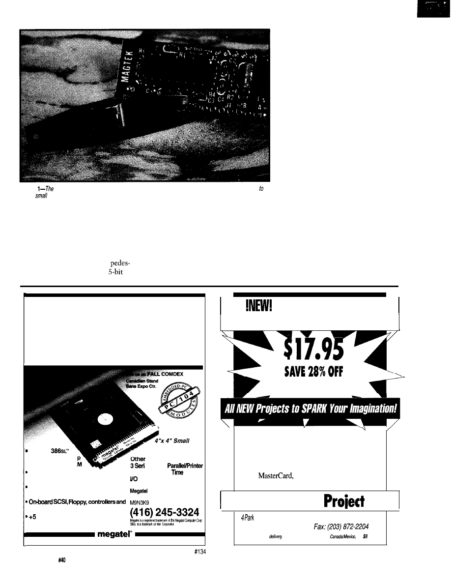
MAGNETIC BIT STORMS
Photo
compactness of the data recovery circuit board and dual-track magnetic pick up make it possible
build a
identification module for use as a card reader for entering your house or garage.
Even the most anemic controller
characters per second, or a new bit
should be able to keep up. With
every 266 us. Since most dual-track
reasonably good coding techniques,
read heads provide track 1 and track 2
there should be no problem handling
data, this indicates that handling both
the entire data sampling phase on an
tracks simultaneously is feasible under
interrupt-driven basis. The low-density
interrupt control. Keep in mind that 50
(track 2) data flows at a more
ips is a rather fast scan rate; 2030 ips
trian 3,750 bps, yielding 750
is probably a more realistic limit.
When approaching a problem such
as decoding magnetic cards, it pays to
spend some time looking at the overall
picture before starting to write the
code. At first glance, it would seem
that organizing the data into the
prevailing element size during the
sampling interval would make decod-
ing easier. This could be easily done by
ignoring all the leading zeros, with
actual data storage commencing with
the first one bit. Of course, this
approach assumes you’re getting good
data. The fact that the data recovery is
handled using well-proven hardware
makes this assumption valid.
If all you need to do is decode the
card in a forward direction, then going
about things as I just described makes
sense and reduces the coding effort to a
trivial exercise. If you have to support
reverse decoding, then this is not the
optimal solution. Having considered
the tradeoffs of being able to decode a
magnetic card in both forward and
reverse directions, I decided to struc-
ture the program to work equally well
Embedded
P C
with on-board
Ethernet
and
Super VGA
25 MHz
CPU; including u
to 18 MByte DRA
On-board Super VGA
LCD/Video controller
On-board Ethernet, Featuring
AUI and 10 BASE-T interfaces
Rugged Format
features include:
al Ports,
port, BIOS, Real
Clock,
Bus Expansion
For more information call:
Computer Corporation
125 Wendell Ave., Weston, Ont.
Fax: (416) 2456505
2 MByte Flash Eprom Solid State Diik
volt only operation,
5 watts power consumption
FROM CIRCUIT CELLAR
PROJECT FILE, VOL. II
COVER PRICE OF $24.95
GPZS Audio Sampling System
Wiring Your House for the 21st Century
Multiprocessor Architecture using DSP
ANDMUCHMORE!!!
VISA,
or International Postal Money
Order (U.S. funds drawn on U.S. bank only)
Circuit Cellar
File
Street
Tel: (203) 875-2199
Vernon, CT06066
‘includes domestic
Please add $6 for delivery to
add for other
non-U.S. addresses
72
Issue
November 1993
The Computer Applications Journal
Listing 2-Once the serial stream has been acquired, the
decoding algorithm takes over.
magnetic track 1 decode routine
sample count in ACC, output: ACC contains character count
DPTR points to decoded data buffer
;Reg. usage for this routine (includes subroutines) as follows:
Direction flag, O=forward
Cumulative LRC register
Decoded character counter
Nondecrementing sample count
Decrementing sample count
Bit synchronizing counter
PROC
pass, setup for forward decode attempt
MOV
forward decode
MOV
to start of buffer
MOV
counter
MOV
count
JMP
pass. setup for reverse decode attempt
MOV
reverse decode
MOV
MOV
count
DEC A
ADD
A,DPL
MOV
DPL,A
CLR A
ADDC
MOV
to end of buffer
MOV
counter
initialization
MOV
counter
in either direction at the cost of a
slight increase in initial complexity.
The first step in decoding is to
acquire the serial bit stream. This can
be done using a dedicated sample loop
or, with a little more work, using
interrupt processing. Since the idea is
the same regardless of the details,
I
decided to use a sample loop in my
demonstration program (Listing
1).
The code simply records the incoming
data stream and deposits the data in a
sample buffer a byte at a time. Sam-
pling begins when Card Present goes
active and terminates when Card
Present returns idle. Any incomplete
byte that has been partially assembled
at the time when sampling terminates
is simply discarded. The abundance of
leading and trailing zeros allows losing
some bits at either end without
causing any problems.
Once the sampling interval
completes, control is transferred to the
decoding algorithm. Presented in
Listing 2, the track-
1
decode algorithm
consists of nothing more than some
initialization and the essence of the
Why pay $30 to $50 for a 3-D Stereogram
at your local Mall when you could
M A K E Y O U R
3-D
and
SOLID OBJECT MODELING
System
Requirements: DOS PC, 386-486 with 4.0
MB RAM,
hard disk,
SVGA
color
mode.
This
full
3-D
object modeling code allows you to
from
rendered
into
your own
random-dotstereogram image.
The system is mouse-driven, contains a basic sketch
binary
file output.
The Computer Applications Journal
Issue
November 1993
7 3
SOLID STATE DISK
Card
2 Disk Emulator
EPROM, FLASH and/or SRAM
Program/Erase FLASH On-Board
Total, Either Drive Bootable
386DX CPU $695”
Compact AT/Bus or Stand Alone
SVGA, IDE, FDC, 2
Drives to
Cache to
DRAM to 48M
TURBO XT
w/FLASH DISK $266”
To 2 FLASH Drives,
Total
DRAM to 2 M
FLASH On-Board
CMOS Surface Mount, 4.2” x 6.7”
2
Par, Watchdog Timer
All Tempustech VMAX products are
PC Bus Compatible. Made in the
U.S.A., 30 Day Money Back Guarantee
*QTY 1, Qty breaks start at 5 pieces.
TEMPUSTECH, INC.
Fax for
fast
response!
295
Airport Road
Naples, FL 33942
Listing P-continued
MOV
L R C
MOV
synchronizer
CALL
FIND-START
decode loop
JNC
bit error
CALL
GET-CHAR
Sentinel
JB
error
CJNE
sentinel error
byte or End Sentinel
CALL
GET-CHAR
JB
error
CJNE
;end sentinel not found
JMP
CALL
STORE-CHAR
character
JMP
;LRC
CALL
GET-CHAR
LRC
JB
error
MOV
JNZ
error
MOV
return
MOV
character count
RET
error, check if 1st pass
CJNE
direction
CLR A
return
RET
ENDPROC
Listing
intermediate layer
is one
removed from the nitty-gritty details.
the next bit from the sample buffer
C contains data bit
GET-BIT
PROC
CJNE
MOV
PUSH
MOVX
CALL
MOV
POP
DEC
XCH
CALL
XCH
DEC
RET
ENDPROC
ACC
ACC
RO
the first ‘1' bit in the samp
if bit is found
FIND-START
PROC
CJNE
MOV
MOVX
CALL
DJNZ
JMP
CALL
LOCATE-BIT
JC
CALL
DEC
RO
JMP
synchronizer
sample counter
bit synchronizer
e buffer
bit synchronizer
sample counter
out of samples
test for a ‘1' bit
bit synchronizer
Issue
November 1993
The Computer Applications Journal
Listing 3-continued
MOV
SETB C
RET
CLR C
RET
ENDPROC
return
copy in B
:bad return
the next 7 bit element from the sample buffer
ACC contains data element
error flag is ACC.7
PROC
MOV
counter
JZ
of samples
MOV
counter
CLR A
CALL
bit
RRC A
DJNZ
RR
A
JNB
error
ANL
parity
PUSH
ACC
XRL
LRC
MOV
R4.A
POP
ACC
RET
return
SETB
ACC.7
;bad return
RET
ENDPROC
Cross Assemblers
Labelsand
Cross Reference
Powerful Macro Substitution Capability
. Machine Cycle Counting
.
32 Significant Character Labels and Symbols
. Unlimited include File Capability
.
Selectable Intel Hex or Motorola Hex Object File
Simulators
Source View Symbolic Debugging
.
Attach Keyboard, Screen or Data Files to Simulate i/O
. Machine Cycle Counting
. Ten User-definable Screens
.
Unlimited Breakpoints, Memory and i/O Mapping
.
Trace File to Record Simulator Session
Disassemblers
Automatic Substitution of Defined Label Names for AI
Jumps and Branches
.
Automatic insertion of Supplied Comments and
Application Source Libraries
l
16 and 32 bit integer Arithmetic and
Conversion
716 Thimble Shoals Blvd.
Newport News, VA 23606
(804) 873-1947
873-2154
BBS: (804) 873-4838
decode logic. Limiting the gyrations
contained in the main body of this
routine not only makes the logic easy
to follow, but permits the same code
to handle the decoding in either a
forward or reverse direction.
The initial entry point assumes a
forward decode attempt and sets up
the necessary flags, pointers, and
counters before jumping into the main
initialization code. After initialization,
the sample buffer is scanned for the
first one bit, at which time a 7-bit
element is assembled. If the parity is
correct and the character code checks
out to be a Start Sentinel, the code
proceeds and starts pulling successive
data elements from the sample buffer.
If the data element is not an End
Sentinel, the character is translated to
ASCII and stored in the decode buffer.
Should an End Sentinel be detected,
the program extracts the next charac-
ter, which is assumed to be the LRC
byte, and finally checks the calculated
LRC for a value of zero.
The checks and balances included
in the execution of this loop include
TW523
Power Line Interface
Developers Kit
Interface Your Computer To Transmit And
Receive X-10 Codes Over Your AC Power Line.
Two-Way Communication.
Real Time Environment Control.
Includes
TW523, Cable, Interface Connector (S/P)
Documentation. Source Code Supplied in
Pascal,
or Run Time.
Disks
Format.
a
Baran-Harper Group Inc.
Voice (905) 294-6473
BBS (905) 471-6776
Fax (905) 47 I-3730
The Computer Applications Journal
Issue
November 1993
7 5
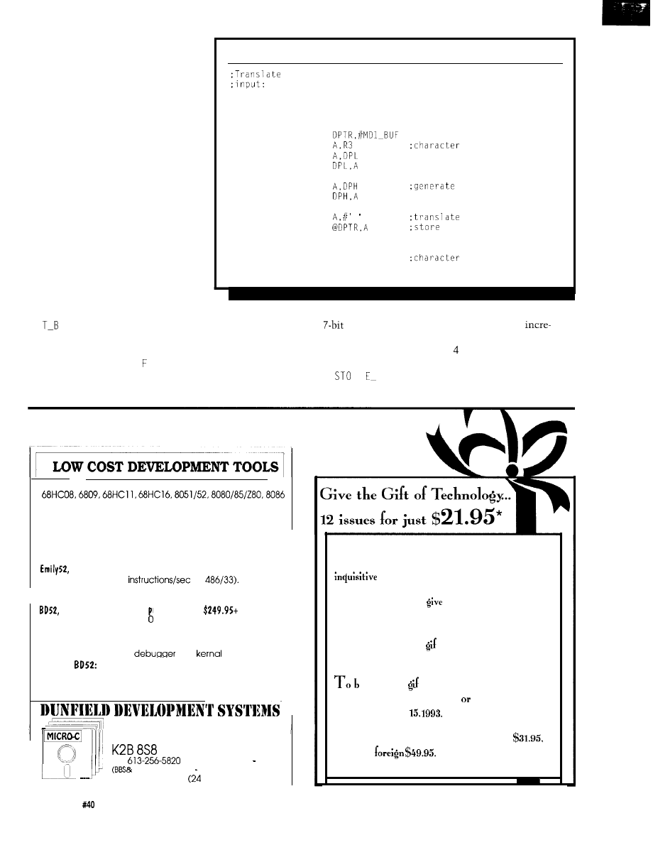
things such as parity, a cumulative
LRC, and checking to make sure I
haven’t run out of samples. If every-
thing checks out, the program termi-
nates and returns with DPTR pointing
to the decoded data buffer and the
character count contained in ACC.
Should a decode failure occur, a test is
performed on the direction flag and if
this is an attempt at a forward decode,
the routine jumps to the reverse
initialization entry point. The reverse
entry is similar to the forward decode
entry but sets up the sample pointer to
the end of the sample buffer and sets
the direction flag to indicate a reverse
operation.
The routines contained in the
intermediate layer are shown in
Listing 3. The meaning and operation
of these routines should be apparent.
The key routine in this section is
GE
I T, which picks off the next bit
from the sample buffer, essentially
restoring the sequential nature of the
initial magnetic bit stream. I ND_
START is used to synchronize with the
first one bit. GET-CHAR first checks to
Listing I-continued
and store the data character
ACC contains data character
STORE-CHAR
PROC
PUSH
DPL
PUSH
DPH
PUSH
ACC
MOV
MOV
counter
ADD
MOV
CLR A
ADDC
displacement
MOV
POP
ACC
ADD
MOVX
POP
DPH
POP
DPL
INC
R3
counter
RET
ENDPROC
make sure it hasn’t run out of samples,
character into its respective location in
then assembles the next
data
the decoded-data buffer and
element while doing a parity test and
ments the character counter.
LRC calculation. Any problems
Listing shows the low-level
encountered here are sent back to the
code. These routines perform the most
caller and are handled there.
R
rudimentary functions and operate in
CHAR translates and deposits the data
accordance with the direction flag.
We have a complete line of ‘C’ compilers
(MICRO-C)
for:
and 8096 processors. Cross assemblers for these plus others.
Source code and porting packages are available!
Development Kits: $99.95 + s&h
Includes C compiler, Cross assembler, ROM Debug monitor,
Library source code, Editor, Telecomm program and every-
thing else you need to do ‘C’ and Assembly language
software development for your choice of processor.
a high speed 8052 simulator: $49.95 + s&h
High speed (500.000
on
Hardware
emulation mode accesses real ports/timers on your target
system. Includes PC hosted “in circuit’ debugger.
a complete 8052 Develo
Everything you need for 8
ment System:
s&h
52 development, including:
Hardware: 8032 based single board computer with 32K
ROM, 32K RAM, RS-232 port, Hardware debug support.
Soflware: DDS MICRO-C Developers Kit, EMILY52 Simulator,
PC Hosted “in circuit”
and
in ROM.
loaded
$299.95 + s&h --
As above, with extra 32K RAM, 4 A/D + 1 D/A, 2K EEPROM,
7 line relay driver, watchdog and power monitor.,
Call or write for our free catalog.
P. 0. Box 31044
Nepean, Ontario Canada
Tel:
(l-5pm EST, Mon Thu)
Catalog Requests 24 Hour with Touch Tone)
Fax:
613-256-582 1
Hour)
Gift subscriptions to the Computer Applications
Journal are available for the technologically
people on your holiday gift list.
It’s
hassle-free! Just
us a call and we’ll set up
your lucky recipient with a full one-year subscrip-
tion to the Computer Applications Journal.
They11 also receive a
t card with your name and
the subscription’s starting issue date.
o e sure your t arrives in time for the
holidays, call (203) 875-2199 fax (203) 872.2204
before December
*Price good in U.S. only. Canada/Mexico
all other
U.S. funds drawn on U.S.
banks only
7 6
issue
November 1993
The Computer Applications Journal
I ND
E
R either increments or
decrements the sample pointer,
P 0 S I T I 0
I T likewise does either a
right or a left shift, and LOCATE-B IT
returns the state of the least- or
significant bit of the accumulator.
GO AHEAD, TAKE A SWIPE
Let me touch on a few additional
points that may not be immediately
apparent before signing off. Storing the
sampled data in a continuous stream
makes the sample routine work
equally well with the various bit
configurations used for the different
recording tracks. This would not be
easily attained if you tried to generate
a particular element format during
sample time. Furthermore, if you look
at the differences between the encoded
character sets and the bit formats for
the different tracks, you will find that
they differ in only a few areas. With a
few minor changes, such as the defined
Start Sentinel, number of bits per
element, and character translation
method, the decode routine I’ve shown
could easily be coerced to handle the
decoding of any of the standard
magnetic tracks.
As a matter of fact, by recoding
and redefining the hard-coded con-
stants as variables, these could be set
up for the particular data track at
execution time before invoking the
decode function. Doing so would not
only save program memory, but would
also allow you to use a routine you
were comfortable with.
Dybowski is an engineer in-
volved in the design and manufacture
of hardware and software for indus-
trial data collection and communica-
tions equipment.
Mag-Tek, Inc.
20725 S.
Ave.
Carson, CA 90746
(213)
Fax: (213) 631-3956
419
Very Useful
420 Moderately Useful
421 Not Useful
Listing
low-level routines get right
to the ground
and take care of all the gory details.
the sample pointer either forward or backward
PROC
CJNE
direction
INC
DPTR
RET
PUSH
ACC
DEC
DPL
MOV
A,DPL
CJNE
DEC
DPH
POP
ACC
RET
ENDPROC
Position bit is in ACC into C in either a right or left shift
PROC
CJNE
direction
RRC
A
RET
RLC
A
RET
ENDPROC
Locate a 1 bit, either msb or lsb; output: C=l if bit is a one
LOCATE-BIT
PROC
CJNE
direction
MOV
RET
MOV
RET
ENDPROC
Frame Grabber
l
$495 Including Software with “C” Library
l
Half
Card for Compact Applications-
l
Real Time Imaging with Display Output
l
8 Bit (256 Gray Levels)
The Computer
Issue
November 1993
77
by becoming programmable through the inclusion of
microprocessors. The second group consists of memory
devices such as EPROMs,
and the like
which are the programmable components used in making
these devices programmable. have elected to report this
month on nine patents chosen from both categories. The
first five abstracts present some novel and interesting
devices which benefit from their programmability; the last
four abstracts present some recent developments in the
creation of new types of memory devices.
Leading off, Abstract
1
presents an alternative to the
often troublesome task of removing and upgrading an
EPROM in a system when changes become necessary. Since
this patent is assigned to Ford Motor Company, one can
presume it is related to engine emission (or other) controls
mounted (perhaps even within sealed packages) in the auto-
mobile. Certainly it is a time-consuming, and hence costly,
matter to access and upgrade the program or parameters
stored in these modules. The approach covered by this
patent permits new code to be loaded instead into an
EEPROM which is part of the system. An address compara-
tor detects the section of old code that is to be redirected to
the new code stored inside the EEPROM. Detection of this
address causes program memory access to switch from the
Patent
Number
Issue
Date
Inventor(s)
Assignee
US References
1990 02 27
Pidsosny, Richard A.; Burke, Michael J.; Jarvis, Mark W.
Ford Motor Company
4,751) 703
Title
Abstract
Apparatus and method for correcting microcomputer software errors
An apparatus for replacing an undesired code stored in a plurality of storage locations in read-only memory (ROM)
with a replacement code. The replacement code, including a jump-back instruction to readdress the ROM, are
programmed into an EEPROM. First and second storage locations store the beginning address of the undesired
code and the beginning address of the replacement code, respectively. When the beginning address of the
undesired code is generated by a program counter, a comparator generates a transfer signal. In response, the
beginning address of the replacement code stored in the second storage location is transferred into the program
counter. Each address of the replacement code is then sequenced by the program counter until a central processing
unit recognizes the jump-back instruction. The central processing unit then readdresses the ROM in response to the
jump-back instruction after the entire replacement code has been executed in place of the undesired code.
Patent Number
Issue Date
1991 01 22
Inventor(s)
Mehta, Hemang S.
Assignee
Chrysler Corporation
U S R e f e r e n c e s
US Class
741843 741844
Int. Class
41
Title
Method of engine model determination for use in an electronically controlled automatic transmission
Abstract
A method of engine determination is used in an electronically controlled automatic transmission system. A transmis-
sion controller is capable of determining the particular engine model by data sent by the engine controller. The
method includes determining whether the data received equals a first predetermined engine model byte stored in
RAM. If not, the method determines whether the data received is valid. If so, the method determines whether the
data received equals a second predetermined engine model byte stored in EEPROM.
78
Issue
November 1993
The Computer Applications Journal
EPROM
to
the EEPROM. A “jump back” instruction
Yet again in the area of automobile control, Abstract 3
turns execution to the original code after the “patch” is
from Delco Electronics Corporation presents an antitheft
executed. Such a technique would seem to have
device. Here again the ever-popular and dynamically
ity in many types of environments other than vehicles.
changeable EEPROM comes to the rescue. In this instance,
Also, an ability to load the EEPROM remotely over a
the value of a resistor pellet mounted in the ignition key is
communication link would further benefit this technique.
measured and compared with a value stored in the
Abstract 2 from another automobile manufacturer, this
EEPROM. A match permits the car to start. Obviously, a bit
time Chrysler Corporation, struck me as an interesting and
novel use of programmability. It also points out how
“electronic” the modern automobile is becoming. In this
situation, the electronic control unit of an automatic
transmission communicates with the electronic control for
the engine to determine which type of engine it is con-
nected to. Presumably, parameters such as shift points are
altered depending upon which engine the transmission is
paired with. Note once again the use of EEPROM to store
variable data which (probably) can be updated whenever the
need arises.
more added intelligence would permit lockout control too.
Together they would provide very inexpensive, yet effec-
tive, protection scheme. The use of EEPROM permits field
changes in the key code so that keys may be changed
whenever the car is sold, for example.
Getting away from automobiles, the next two patents
relate to smart circuit breakers. While to most of us a
circuit breaker is a pretty mundane device, the future holds
programmable breakers with interesting intelligence built
in. Abstract 4 from Westinghouse presents a microproces-
sor-based circuit breaker with a removable “rating plug”
Patent
Number
Issue Date
Inventor(s)
Assignee
US References
US Class
Class
Title
Abstract
1991 02 05
Curtis N.; Griffin, R.;
John M.; Nemirovsky, Mario D.
Delco Electronics Corporation
Programmable vehicle antitheft system
A vehicle antitheft device is disclosed which includes an electronically erasable programmable read-only memory
(EEPROM) which stores a modifiable code which must be matched by an input code in order to start the vehicle.
The ignition key includes a resistor pellet, engaged by contact in the ignition lock assembly, which is measured to
provide the input code. To avoid problems associated with intermittent contact engagement with the resistor pellet,
circuitry is provided to control the resistor measurement cycle.
Patent Number
Issue Date
199009
Inventor(s)
Murphy, William J.
Assignee
Westinghouse Electric Corp.
US References
4,351
3
25
US Class
Int. Class
361
Title
Circuit breaker with rating plug having memory
Abstract
A microprocessor-based circuit breaker has a removable rating plug which provides a reference for the current rating
of the breaker. The removable rating plug also has an EEPROM to which the microcomputer of the circuit breaker
writes for storage, the number of operations of the circuit breaker operating mechanism, and a trip history of the
breaker in the form of a count of the number of trips weighted by the magnitude of the trip current. The rating plug is
periodically removed and plugged into a portable programmer which selectively displays the number of operations
and operating history of the circuit breaker. The programmer clears this operating data when recorded and can write
into the EEPROM the style and serial number of the circuit breaker with which the rating plug is to be used.
The Computer Applications Journal
Issue
November 1993
which determines its trip point. Our friend the EEPROM
once again comes into play. It is used in the removable plug
to store such information as the number of operations of
the breaker and at which levels of trip current they oc-
curred. The plug may be removed and its stored informa-
tion downloaded to a special unit which may also write
information back to the plug in order to specify valid usage.
Abstract from Square D Company presents another
variation on the “smart circuit breaker” concept. In this
measure, calculate, store, communicate, and regulate many
types of quantities and information.
As promised, the final three abstracts present some
recent developments in the fabrication of programmable
memory elements. While I am not personally aware of such
devices being available currently, it will be interesting to
see when they appear and how they will be used. Intel, in
Abstract 6, presents a process for simultaneously fabricating
both EEPROM and flash EPROM cells together on the same
case, the patent attempts to be considerably broad,
material. Such a dual-type memory element would present
ing the use of the microprocessor and EEPROM memory to
useful and interesting possibilities in compact system
Patent Number
Issue Date
1991 02 26
Inventor(s)
Farrington, Ronald L
Assignee
Square D Company
US References
4 5 3 5 , 4 0 9
US Class
Class
3641483
32E 3401657
3641492
GO1
Title
Abstract
Microprocessor-controlled circuit breaker and system
A circuit breaker system uses a microprocessor for calculating at least one function of a measured current flow. The
microprocessor provides other functions such as serial data stream communications, the ability of many circuit
breaker systems to communicate with a central computer, storage of trip information concerning the last trip, storage
of historical trip information concerning a number of past trips, EEPROM memory for storing trip information. The
microprocessor may inhibit tripping on a high-current fault to permit storage of trip information into a memory. Power
is derived from current transformers drawing energy from current flow to a load and the electronics are protected
from high voltage caused by heavy current flow to the load. Optical isolators are used for the circuit breaker to
communicate with external equipment, a multiturn resistor adjusts an external test voltage for testing the circuit
breaker system, in the event that there is no load or a load drawing insufficient current to provide power for the
electronics the circuit breaker may be externally powered to provide readout of electrically erasable programmable
read only memory, the microprocessor reads setting switches and a multiplier plug. The microprocessor is capable of
digitizing selected quantities frequently and of digitizing other quantities less frequently. A second microprocessor
permits one microprocessor to sample voltage and current rapidly for metering purposes, and the second micropro-
cessor operates other functions.
Patent Number
Issue Date
Inventor(s)
State/Country
Assignee
19900918
Tam, Simon M.; Lai, Stefan K.
C A
Intel Corporation
US References
US Class
Int. Class
437143 437144
4371193
HO1 L 21170
Title
Process for simultaneously fabricating EEPROM cell and flash EPROM cell
Abstract
Improved processing which permits the simultaneous fabrication of block erasable flash EPROM cells and individu-
ally erasable EEPROM cells. A polysilicon finger extends from the floating gate of the EEPROM cell over a tunnel
oxide region. Doped regions are formed under this finger by implanting
in alignment with the finger during
the implantation of the source and drain regions for the cells and then driving the
under the finger. The
arsenic
used to form the source and drain regions for the cells is used to form the doped regions along with
the phosphorus
used for the source region of the flash EPROM cells.
0
Issue
November 1993
The Computer Applications Journal
Patent Number
Issue Date
1991 1224
Inventor(s)
State/Country
Assignee
US References
US Class
Class
Title
Semiconductor memory device having a volatile memory device and a nonvolatile memory device
Abstract
Yamauchi, Yoshimitsu; Tanaka, Kenichi; Sakiyama, Keizo
JPX
Sharp Kabushiki Kaisha
3651228 3651149 3651185 357123.5
A semiconductor memory device composed of a DRAM, an EEPROM, a mode switch means for selecting
either mode of the DRAM mode and the EEPROM mode, and a transfer means for transferring data stored in
the DRAM to the EEPROM and vice versa. The DRAM consists of one transistor and one capacitor, and one
of the terminals of the capacitor is electrically isolated.
Patent Number
Issue Date
1991 08 27
Inventor(s)
State/Country
US References
US
Class
Int. Class
Title
Abstract
Harari, Eliyahou
CA
68
85 3651218
0
Flash EEPROM memory systems having multistate storage cells
A memory system made up of electrically programmable read-only memory (EPROM) or flash electrically
erasable and programmable read only memory (EEPROM) cells. An intelligent programming technique allows
each memory cell to store more than the usual one bit of information. An intelligent erase algorithm prolongs
the useful life of the memory cells. Use of these various features provides a memory having a very high
storage density and a long life, making it particularly useful as a solid-state memory in place of magnetic disk
storage devices in computer systems.
Patent Number
Issue Date
Inventor(s)
Mitchell,
T.; Tigelaar, Howard L.
Assignee
Texas Instruments Incorporated
US References
US Class
Class
Title
Abstract
1992 1027
85
82
Four memory state EEPROM
An EEPROM memory cell having sidewall floating gates is disclosed. Sidewall floating gates are formed on
sidewalls of a central block. Spaced apart bit lines are formed to serve as memory cell sources and drains.
Sidewall floating gates are capable of being programmed independently of one another. When control gate is
actuated and either bit line or bit line is used to read the device, four separate memory states may be
identified depending on whether either, neither, or both of the sidewall floating gates have been programmed.
Issue
November 1993
The Computer Applications Journal
TALK
applications. In particular, I think they would make an
intriguing memory card device which could be used to store
both program and data concurrently. Also, such a device
would directly support Ford Motor Company’s code
patching technique presented above in Abstract 1.
In a similar vein, Sharp presents in Abstract 7 a novel
programmable memory device which is both DRAM and
EEPROM. Presumably, the combination of the two devices
into one unit offers the designer the benefits of both: fast
access time and unlimited read/write capability of the
DRAM coupled with low power and nonvolatility of the
EEPROM. Keep a sharp eye for this one to hit the market.
Finally, the potential benefits of multivalue storage, in
contrast to binary only, has long been known but seldom
used. Abstracts 7 and 8 present two approaches to storing
more than one bit of information per memory cell. Perfec-
tion and commercialization of such techniques could
achieve a new horizon in storage capacity and memory
system design. And as we approach physical speed barriers
in component design, coupling such memories with multi1
processing elements could be one way to tackle the
esign of yet faster computers.
q
Russ Reiss holds a Ph.D. in
and has been active in
electronics for over 25 years as industry consultant,
designer, college professor, entrepeneur, and company
president. Using microprocessors since their inception, he
has incorporated them into scores of custom devices and
new products. He may be reached on the Circuit Cellar
BBS or on CompuServe as
Patent abstracts appearing in this column are from the
Automated Patent Searching (APS) database from:
25 Science Park
New Haven, CT 065
11
(203)
or (800) 648-6787
422 Very Useful
423 Moderately Useful
424 Not Useful
DO YOU NEED CONTROL ?
If you’re looking for a temperature sensor that
allows your computer to not only monitor the
temperature but respond to it
look no further.
Temp-A-Chip,, is a solid state temperature
sensor providing truly linear measurement of
temperature. The
is an
intelligent, user configurable sensor which
interfaces with your computer. No batteries are
needed to operate the
, it plugs
into any standard RS232 interface.
LCD Display
Solid State Design
No Batteries Req’d
RS-232 Interface
Easy To Install
Easy To Use
Can You Afford Not to Call Today?
$149.
$5.00 P H
The new high-performance software analyzer that
captures, time-stamps, and records software and hardware
interrupts, DOS calls, BIOS interrupts, and user-defined
events
in real-time for analysis of race conditions,
interrupt activity, and service times.
you
the hard facts you need to fix the big one that stands
between system test and shipping your product.
Figure 1. Detailed timestamping C library
function call.
If
can break-down a library function call into
its components (above), imagine how you’ll see context
switches, device interrupts, and other asynchronous code.
Cdl
for
technical
GENERAL
Tel
206.39 1.4285
SOFTWARE
Fax
Box 2571, Redmond, WA 98073
BBS
1993 General
Al
de logo, ond
of
I
N
.
The Computer Applications Journal
Issue
November 1993
83
The Circuit Cellar BBS
bps
24 hours/7 days a week
(203)
incoming lines
Internet
In case you missed my editorial on page 2, let me give you the
exciting news here: Circuit Cellar is now accessible through Internet
Now before you get too excited, the BBS is not accessible via
telnef or
ftp. Right now the cost
such access is outra-
geous. Instead, you may send us mail through the Internet and also
pick up magazine-related files using ftpmail.
Additionally, all users who call into the Circuit Cellar BBS via
modem automatically get an Internet address and may send and
receive Internet
using the
BBS as their gateway. Simply put a
period between your first and last name, add our domain name to the
end, and you have your Internet
address. For example, my
address is
There is lots more you can do, too. For all the information, call
the BBS and download the information file available on-line, or send
an
message to
and include the phrase
“get he/p. txt” in the body of the message (not
in the subject field).
will be
mailed back to you automatically.
On to the messages at hand. We start out this month with a
discussion about using
transformers on
lines and
versa. not an open-and-shut issue. We conclude with a look at
how to control a small DC motor using a microcontroller.
Transformer Frequencies
From: RONALD HATCHER To: ALL USERS
Does anyone know what is involved in changing a
V,
AC current to 120 V, 60 Hz?
From: LARRY G NELSON To: RONALD HATCHER
have done it with a solid-state converter and also with
a motor generator set. There is no way to change the
frequency with a simple transformer. The application you
have may not care about the frequency, in which case a
transformer can be used.
From: PAUL PETERSEN To: RONALD HATCHER
Yes, you need a step-down transformer available at
most any electrical wholesale house. Don’t worry about the
difference between 50 Hz and 60 Hz since the transformers
are broad enough to accommodate both.
84
Issue
November 1993
The Computer Applications Journal
From: TOM
To: PAUL PETERSEN
Yes, you do need to worry about
Hz when you
select a transformer. Some are 50, some are
and SOME
are broadband, designed to handle both. If you connect a 60
to a
line, you will end up with smoke.
From: PELLERVO
To: TOM
I want to qualify your smoke statement. The frequency
rating alone is not enough, although your choice is basically
correct: the
transformer is endangered on a
line. But that is, if they have identical voltage ratings and
then you apply exactly the same FULL voltage. The rule is
that the magnetic path can take a certain amount of
magnetic flux, depending on the size of the core. Given this
number (which, by the way, is dependent on the
section and the length of the path due to leakage effects
and, more than anything, it is dependent on the material of
the core), you can apply up to a maximum magnetizing
CURRENT to a winding of any given number of turns.
All this is in DC sense. When we start talking about
transformers, we are also talking about AC and we tend to
prefer talking about voltages instead of currents. Now, the
rules get changed a little, just like a special kind of trans-
former [pulse transformer) is actually
by the
volt-second figure it can handle. Either a higher voltage or a
longer time will bring it to saturation.
The inverse of time is frequency, so we can see that the
possible voltage rating for any given transformer is directly
proportional to the frequency (if we want to bring it to the
edge of saturation). Therefore, a given 50-Hz transformer
will always sustain the same amount of voltage at 60 Hz or
it can even be rated 20% higher. But the opposite direction
of conversion of course requires derating.
All of this is assuming a razor sharp saturation and a
design driven to the leading edge in materials and weight
saving. But most magnetic materials in use have quite
rounded saturation characteristics and most transformers
have had to be designed with a voltage range allowance, say
With this and a checking of the available voltage, I
might sometimes conclude that it is safe for *me* to
connect a
transformer to the
line in
Europe. And actually, there are both core losses and copper
losses to consider. If the transformer secondary load is
negligible, maybe it would tolerate some amount of
saturation-caused increase in the primary current as well as
the higher core temperatures.
Going the other way round-using a transformer at
elevated frequencies-the main issue is the eddy current
losses at the higher frequencies increasing according to a
square law, if we increase the voltage proportional to the
frequency. However, if we keep the voltage the same, the
eddy current losses do not grow that bad. I would say most
any ordinary
power transformer can run quite well at
400 Hz. Maybe some transformers that have their cores
welded for cheap manufacturing start suffering a little more
than those with hand-stacked laminations and insulated
screw assembly, but the difference is still minimal. How-
ever, I would not try to use an ordinary power transformer
even at reduced voltages as an output transformer for an
audio amplifier.
Here is again the formula that governs transformer
designs (after you have picked a core):
where
n is the number of turns in the winding (each individu-
ally)
V is the RMS voltage of sinusoidal excitation
f is the applied frequency in Hz
b is the *peak* magnetic flux density allowable in
teslas
(10
A is the cross-section of the core in square meters
The 4.44 happens to be the product of pi and square
root of 2, for those curious about this detail.
Another detail, that would need to be covered for a real
treatise of the transformer design is the selection of the core
based on the power requirement. Mostly it is handled by
picking the value from the data sheet of a magnetic mate-
rial manufacturer. But there is a way to estimate it, if you
are willing to make fully custom coil former as well. The
rule is that the cross-section of the iron core should be
about as much as the “window” space for all the windings
combined. This leads into iteration: Assume some
section, see how many turns it would require, and see if
that many turns fit into HALF the window size (assuming
you start the calculation with the primary that takes half of
all winding space, with all the secondaries sharing the other
half). Assume each wire turn occupies a space that is the
square of the insulated wire diameter and that the wire can
handle a conservative
1.5
or a little more demand-
ing 2.5
Adjust your guess for the core cross-section
and window size, and repeat until you reach an optimum
design.
Sorry to become so wordy, but I think this issue is of
such universal importance to any electronic designer to
understand that I just could not stay away.
From: TOM MAIER To: PELLERVO KASKINEN
was
an engineer for four years at a company that made
machines for world wide market. I know too well what
happens if the wrong transformer gets used.. the engineer
gets his butt kicked!
From: PELLERVO KASKINEN To: TOM MAIER
By now I have been in a similar position for
15 years. So
far no kicking to the butt, but then I think this issue has
always been dear to me. On the other hand, the purpose of
my previous message was the benefit of the general audi-
ence as I said.
Actually, I have started suspecting that the flow of
information on this board is so rapid that many people
cannot find the topic after a few months even with the
subject search. I keep getting so much from the discussions
here that I feel a need to contribute and to stay with my
style, go down to the details where I can. So, in this case,
for instance, my recollection was that this transformer
topic was covered too long a time ago to have stayed
accessible. That’s why you got the message that you
probably did not need. And that people who just call to ask
a question and then call back to read the answers directly
addressed to them are still going to miss it-too bad!
From: TOM MAIER To: PELLERVO KASKINEN
You
gave a great answer. At one company I worked at
we shipped around the world and occasionally we would
assign the wrong transformers. got caught in that once and
it is now burned into my memory that 50 Hz is very
different from 60 Hz.
From: DAVID
To: TOM MAIER
I think you just have to derate the transformer
of
its power rating..
From: TOM MAIER To: DAVID
Wrong.. With no load you can burn up a 60-Hz trans-
former by connecting it to
power. I’ve seen it done
with
transformers. Sizzle, sizzle, smoke, POW!
The impedance of the primary is not right at different
frequencies. With a
coil run at 50 Hz, you get large
current flow in the primary, higher than it’s rated for. This
The Computer Applications Journal
Issue
November 1993
8 5
is why the transformer gets hot and fries it primary wind-
ings and shorts out. You can, of course, design the trans-
former to handle this, but it increases the cost. Therefore, if
you are designing a cost-sensitive application for U.S. or
European release only, then it is more economical to use
the transformer for your frequency of interest. Shipping
weight is also important on quantity items.
The international company that I worked for finally
decided it wasn’t worth the headaches and went with the
heavier, more expensive
primary isolation trans-
former. The increased cost of the transformer was cheaper
than the cost of stocking two of them and trying to decide
with products got which transformers. Two different stock
items and two different resulting products resulted in a
paperwork increase and occasional shortage of one product
and too much of the other.
If it doesn’t said
on the label, then don’t trust it
to be both.
Also, you have to watch your motors and relays and
solenoids. Same story on those. it doesn’t specifically say
and you plug a 60 into a 50 power, you get smoke.
Plug a 50 into 60 and you get reduced power out (solenoids
won’t activate, motors have half torque, transformers have
reduced output).
DC Motor Control
From: MARK
To: ALL USERS
would appreciate being pointed in the right direction.
I would like to learn about the basics on motor control
(small DC motor) with a microcontroller. I figured it may
be something like this: DAC to preamp (maybe another
preamp) to final drive amp. Nothing fancy to start with.
Books or literature that are light in math, and more for the
technician. Thanks for the help.
From: PELLERVO
To: MARK RUBINO
can only cover some basics from the motor end, not so
much the computer connections or algorithms.
Your assumption about a DAC to preamp and power
stage is basically correct, even though the DAC can be
implemented in direct pulse-width-plus-filtering fashion
instead of the R-2R ladder fashion in some cases. In other
words, the processor is using a timer instead of a parallel
port to drive the speed command line. You can get the
basics from a Hewlett-Packard motor control chip data
sheet or from a similar publication by Galil. Also, National
Semiconductor has something more remotely related to the
86
Issue
November 1993
The Computer Applications Journal
topic. Sorry, did not remember these chips earlier so
could have picked the part numbers for you.
As to the small DC motors, we would need to define at
first the salient points of your interest. Exactly how small?
What speed range? What speed accuracy? All of these affect
the preferred solution very strongly. Also, are you talking of
a pure speed control or also a position control? And does the
position have to be absolute within one session, absolute
even after power down, or is it just relative “now that we
are here, move so much to this direction.” All of the
position-related stuff needs some sort of encoder or other
position feedback sensor. For a computerized system,
encoders are a natural choice, while for a direct amplifier
solution, a potentiometer would do just fine. And for the
encoders, a normal solution is to have a low-cost incremen-
tal encoder plus possibly some limit switches for establish-
ing a home position [for one session only; must be repeated
after each power up). Some fancy systems use either an
absolute encoder or a resolver to establish a known position
even through power down.
Then to the motor. am not going to touch the
brushless variety, just the plain old brush-type motor with a
permanent magnet field. The simple mathematical basis for
them is that they *generate* voltage when they run
proportional to the strength of the magnetic field and the
rotation speed as well as the number of wire turns in the
armature winding. This generated voltage is called back
EMF. Now, there is also some resistance in the armature
winding and a small drop in the brushes/commutator. This
drop is more or less constant, just like that on semiconduc-
tor diodes, though generally smaller, about 0.1
to
0.2 V. And
then, something supplies the driving power, say we have a
battery for the beginning.
One more principle for the preparations: a motor
develops torque proportional to the
l
current (and to the
magnetic field). So what happens when you connect this
small motor to a mechanical load and to the battery is this:
At first, the motor speed is zero, no counter EMF. The
current drawn from the battery is (battery voltage -brush
drop)/(circuit resistance).
The circuit resistance may consist of additional
elements besides the armature, but we get back to the
importance of the armature resistance shortly. With this
current, the motor develops torque and starts accelerating.
don’t complicate the presentation with any changing torque
requirements such as fans or blowers. But the principle is
that the acceleration continues until the motor torque just
matches the load torque requirement.
All along, the motor develops higher and higher
counter EMF. With that, the *apparent* battery voltage
drops, so the current drops. Let’s repeat the formula:
Current = (Battery voltage Brush Drop
Resistance). And the other formula: Output Torque =
(Constant K times Current). The constant K is winding and
magnet strength dependent, but constant for each motor.
OK, back to the speed CONTROL issue. You need to
know the actual speed in order to control it intelligently.
You have several options. A
generator is one. The
pulse frequency from an encoder is another possibility. And
typically the resolver interfaces produce a speed output
signal as well. But if you do want to make it really small
and simple, you do not have the luxury of separate
measuring devices.
Remember the counter EMF. It is proportional to the
speed. But the terminal voltage to the motor is not the same
as the EMF. No, it is the sum of the EMF and the product of
current and armature resistance. So, you just have to know
the armature resistance and the actual current to be able to
calculate the EMF from a measured terminal voltage. You
get the current by inserting a small resistance in series with
the motor and measuring two voltages instead of the
terminal voltage alone. Typically this is done in the analog
domain, but if you have a computer with an A/D converter
(in addition to the DAC), then you can do it digitally.
I hope this covers some of the issues, even though I did
not give any sources for reading. All this comes just from
my own head and is based on something I have had to learn
in the past over and over again, so I could possibly quote
them while sleeping.
From: ED
To: PELLERVO
As an aside on absolute position sensing, the June “HP
Journal” showed a truly neat trick for sensing the position
of the follower on a leadscrew. The thing you want to avoid
is running the follower all the way to the end every time
you power up.. .but you don’t want to spend big bucks for
an absolute encoder with lots of precision.
The encoder uses three gears: one driven by the motor
and two idler gears. Each gear has a hole sensed by a simple
optical interrupter. The trick is the number of teeth on each
gear: they’re relatively prime so the same alignment won’t
come up twice in the length of the leadscrew. The example
they used was a driver gear with 23 teeth and idlers with 24
and 25 teeth. The positions repeat every 600 (= 24 x 25)
revolutions of the driver.
D
oes your Big-Company marketing
department come up with
more ideas
than the engineering department can
cope with?
Are you
a small company
that can’t afford a full-time engineer-
ing staff for once-in-a-while designs?
Steve Ciarcia and the Ciarcia Design
Works staff may have the solution. We
have a team of accomplished program-
mers and engineers ready to design prod-
ucts or solve tricky engineering problems.
Whether you need an on-line solution for
a unique problem, a product
for a startup venture, or
just experienced con-
the Ciarcia
Design Works is ready
to work with you. Just fax me your
problem and we’ll be in touch.
Optional windows software
with powerful binary
editor Available
l
Emulates 64 Kbit to 8 Mbit
EPROMs.
l
Accepts Binary, Ext. Intel Motorola formats.
l
Fast download from printer port (1
l
Fits into EPROM socket to minimize noises.
l
Double sided SMT (size:
l
Jumperless configuration through software.
l
Ni-Cd battery backup. Power-up emulation.
l
Cascadable to 128 bits. Generates RESET+/-.
l
Comes complete with software and cables.
15
DAY MONEY-BACK GUARANTEE.
85ns
$4951695
(213) 664-8909
2750 Riverside Dr.
LA, CA 90039
The Computer Applications Journal
Issue
November 1993
8 7
To sense the absolute position (on power-up, for
example) you turn the driver gear one revolution. You know
when each hole shows up and thus the position of each
gear. That gives you the “turn number” because those
positions are unique within the 600-turn sequence.
Bingo..
now know where the follower is positioned on
the leadscrew! Because you make only a single leadscrew
rotation, the follower doesn’t move very much and you
don’t have to worry about smashing into anything.
From: PELLERVO KASKINEN To: LARRY G NELSON SR
(I think you might have to make slightly more than one
turn to guarantee that each hole passes under its sensor.. .or
perhaps the lack of a hole tells you where it must be!)
From the way they describe it, it’s surely patented and
all that, but it’s a truly neat hack nonetheless.
I have used the back EMF as well for feedback. It is
applicable, when the inertia is high enough and the induc-
tance in series with the motor armature is low enough.
Actually, one more condition is required. It is that the
driver side can be put into a high-impedance state. Then,
when you wait until the inductive current has decayed, you
get the speed proportional and properly dependable signal.
Good for a couple of percent linearity and accuracy.
The complications for my designs seem to be related to
the efficiency of the motor when the current is periodically
interrupted, jerks in speed when the inertia is small, and
when the standard series inductance is pretty large.
From: LARRY G NELSON To: PELLERVO KASKINEN
From: JOHN
To: MARK
One technique I have used in the past is to drive the
DC motor with a PWM signal to control the speed. With
the PWM output off, you can measure the voltage across
the motor and read the back EMF. This voltage is propor-
tional to the motor speed and can be used for control.
An easy explanation of how to control motors is given
in Chapter
13,
“Robot Locomotion with DC Motors,” in
the “Robot Builder’s Bonanza” (book) by Gordon McComb.
I have built the circuits on pages 101 and 103, and they
work very well. In his design, Mr. McComb uses power
which are adequate, however, a number of
manufacturers make single IC H-bridge controllers. Sprague
and RCA (SK brand) are just two manufacturers.
n
mapped variables
In-line assembly language
option
Compile time switch to select
805
or
Compatible with any RAM
or ROM memory mapping
n
Runs up to 50 times faster than
the MCS BASIC-52 interpreter.
n
Includes Binary Technology’s
cross-assembler
hex file
Extensive documentation
n
Tutorial included
Runs on IBM-PC/XT or
Compatible with all 8051 variants
508-369-9556
FAX 508-369-9549
q
Binarv Technoloav, Inc.
P.O. Box 541
l
Carlisle, MA 01741
8 8
Issue
November 1993
The ComputerApplications Journal
We invite you call the Circuit Cellar
BBS
and exchange
messages and files with other Circuit Cellar readers. It is
available 24 hours a day and may be reached at (203)
1988. Set your modem for 8 data bits, 1 stop bit, no parity,
and 300, 1200, 2400, 9600, or
bps. For information on
obtaining article software through the Internet, send
to
with the phrase “get
in
the body of the message (not in the subject field).
Software for the articles in this and past issues of
The
Computer Applications Journal
may be downloaded from
the Circuit Cellar BBS free of charge. For those unable to
download files, the software is also available on one 360K
IBM PC-format disk for only
$12.
To order Software on Disk, send check or money order
to: The Computer Applications Journal, Software On Disk,
P.O. Box 772, Vernon, CT 06066, or use your VISA or
Mastercard and call (203) 8752199. Be sure to specify the
issue number of each disk you order. Please add $3 for
shipping outside the U.S.
.
425 Very Useful
426 Moderately Useful
427 Not Useful

Lest We Forget that Chips
Will
who knows me knows have a favorite programming language. But it’s not easy, or economical, to
program in just one language anymore. It used to be that you could build the keenest computing device with just
one VW bus full of parts, about 15 pounds of solder, spools of different colored wires, and any
the times, they are a changing.
Now I can cram the equivalent of that whole VW full of parts into a couple of square inches. And miles of connections can be
replaced with a couple dozen two-inch traces between
chips. The trouble is now I have to program
When the
first generation of programmable silicon appeared, you still had to use dozens of discrete logic chips and “program” the system with
yards of colored wire. And if the system didn’t work right, could at least verify the connections between the components. Usually, after
correcting the wiring errors, everything would be fine. One of the best features of discrete logic design is that testing it is pretty
straightforward. An AND gate always acts like an AND gate. Nowadays, however, a chip can be programmed to act like anything!
I watched while one of my friends built his newest brainchild. This chap was busy programming nearly every component that was
part of his project. He was programming the processor in C and assembly language. He was also programming several of his logic
components in a variety of
Certain parts download their behaviors on power up, and others’
behaviors were held in an EPROM
image inside the parts. The design of this system was inside of the parts
the way they were connected. He had a host of
programming environments, a bench full of programmers, and a variety of conversion instruments so that all of these parts could be
given its dose of intellect. How does he test a design where every chip is programmed? With other programs (simulators), or with
programmable test jigs. This works great as long as the only bugs he has to deal with are his own.
I remarked at how his project seemed to be missing the characteristic snarl of wire that I associate with prototypes. He looked at
the pristine landscape of his creation and grinned. “Steve, don’t let appearances fool you. It might look like this on the surface. But that
is only because the intractable mass of wires and cables have been replaced with a few thousand lines of code.”
I guess things really aren’t that different after all. When my old projects began to outgrow the circuit board, I would add another
card for the new parts and patch the new circuits to the old ones with a few yards of colored wires. As his projects grow, he does the
same thing. Only he just adds gates in increments of a-sea-of-gates at a time, and all his patches are done in code. And I suppose it’s
just as easy to find a missing or misdirected line of code as it is to find a missing or wrong connection in the wiring.
But, the biggest problem with programmable hardware is environmentally generated software. That’s what happens when your
device gets too close to the ventilation motor and the RFI reprograms your parts for you. When this happens, your chips can
completely forget what you told them, or worse yet, they can learn something completely new and exciting! In either case, now your
code is running along with a new subroutine called chaos. This kind of situation is pretty hard to fit into the design-for-test paradigm,
even if you could model it in the first place. Is there any test method in existence that can trigger on and correct the behavior of
misdirected electrons? Sure, the chances of quantum programming are slim, but there is an unfortunate corollary to Murphy’s law that
states the first occurrence of a quantum-well electron failure will happen at a million dollar account or in a satellite orbiting Mars.
96
Issue November 1993
The Computer Applications Journal
Wyszukiwarka
Podobne podstrony:
circuit cellar1996 11
circuit cellar1994 11
circuit cellar1997 11
circuit cellar2004 11
circuit cellar2000 11
circuit cellar1995 11
circuit cellar2002 11
circuit cellar2001 11
circuit cellar2003 11
circuit cellar1996 11
circuit cellar1995 11
circuit cellar1996 11
circuit cellar2003 11
circuit cellar1997 11
circuit cellar1993 11
więcej podobnych podstron