Weaving the Web
believe it was Charlotte the spider who first
published on a web (remember Charlotte’s Web?).
‘By weaving words for all to see, a
tiny creature
communicates to the world.
Such is the case
with the World Wide Web. The
Web gives even the
smallest of individual the capability to publish something for the world to see
without the expense of printing and distribution.
The growth of the
Web over the past year has been remarkable. Only a
year ago, the first version of
was released and immediately
rocketed to the top of the popularity
charts.
During that time, I’ve received
dozens of messages asking when we’re going to put up a Circuit Cellar Web
page.
I’m happy to announce that we’ve done just that. As with most Web
pages, this one still needs work and will be continually evolving. Currently
available is subscription information, an ftp link to many of the
related files from the most recent issues, our author’s guide, next year’s
upcoming themes and deadlines, results from this year’s Design Contest
(over a month before you’ll see them in print), and more.
We first tied into the Internet over two years ago with an E-mail
connection to the Circuit Cellar BBS. Our Web page marks our continued
commitment to keeping in touch with our readers and providing up-to-date
technical information.
How do you connect? Point your Web browser to http://
The pages are designed for Netscape, but look fine
with other browsers. Let me know what you think.
Onto the
hand. Many engineers tend to think of amplifiers,
filters, and wireless communications when asked about analog design. Our
first article illustrates there is more to analog than signal processing. Analog
computers have played an important role in the past, and their usefulness
today can’t be denied. You just have to train yourself to think analog.
Another computing tool that has been around for a while but just hasn’t
caught on is the transputer. If you’ve heard about them but don’t know quite
what they’ll do, check out how to design a PC plug-in board using an array of
transputers.
A big stumbling block in many embedded software design cycles is
waiting for real hardware to test your code. Our next article shows some neat
techniques for simulating hardware devices on the test bed.
In our last feature article, we wrap up the series on designing an
engine-control system. This enormously popular series concludes with
interesting accounts of the final testing and fine-tuning phases.
In our columns, Ed looks at interrupt processing in Virtual-86 mode,
Jeff selects a low-cost power-line modem chip, and Tom follows up last
month’s video-processing chip overview by covering similar
processing silicon.
CIRCUIT
T H E C O M P U T E R A P P L I C A T I O N S J O U R N A L
FOUNDER/EDITORIAL DIRECTOR
Steve Ciarcia
EDITOR-IN-CHIEF
Ken Davidson
SENIOR TECHNICAL EDITOR
Janice Marinelli
TECHNICAL EDITOR
Carole Boster
ENGINEERING STAFF
Jeff Bachiochi Ed Nisley
WEST COAST EDITOR
Tom Cantrell
CONTRIBUTING EDITORS
Rick Lehrbaum
Russ Reiss
NEW PRODUCTS EDITOR
Harv Weiner
ART DIRECTOR
Lisa
PRODUCTION STAFF
John Gorsky
James Soussounis
CONTRIBUTORS:
Jon Elson
Tim
Frank Kuechmann
Pellervo Kaskinen
PUBLISHER
Daniel Rodrigues
PUBLISHER’S ASSISTANT
Sue Hodge
CIRCULATION MANAGER
Rose
CIRCULATION ASSISTANT
Barbara
CIRCULATION CONSULTANT
Gregory Spitzfaden
BUSINESS MANAGER
Jeannette Walters
ADVERTISING COORDINATOR
Dan Gorsky
CIRCUIT CELLAR
THE COMPUTER
JOURNAL
is published
monthly by Circuit Cellar Incorporated, 4 Park Street,
Suite 20, Vernon, CT 06066 (860) 675.2751. Second
One-year
rate U.S.A. and
$49.95. All
orders payable in U.S.
funds only,
postal money order
check drawn on US. bank.
orders
and
related questions to
Cellar INK
P.O. Box 696. Holmes, PA 19043.9613
or call (600)
POSTMASTER: Please send address changes to
Dept.,
Holmes,
PA
Cover photography by Barbara Swenson
PRINTED IN THE UNITED STATES
For information on authorized reprints of articles,
contact Jeannette Walters (860) 875-2199.
ASSOCIATES
NATIONAL ADVERTISING REPRESENTATIVES
NORTHEAST
SOUTHEAST
MIDWEST
WEST COAST
MID-ATLANTIC
Collins
Nanette Traetow
Barbara Jones
Barbara Best
(305) 966-3939
(708) 357-0010
Shelley
(908)
741-7744
Fax:
(305) 985-6457
Fax:
(708) 357-0452
(714) 540-3554
Fax: (908)
Fax: (714)
bps.6 bits.
1
3600 bps
HST.
World Wide Web.
All programs and
been carefully
to ensuretheir performance
transfer by subscribers.
these
schematics
the consequences of any such
because of
the quality and
of materials and
of reader-assembled
Circuit Cellar
any
for the safe and proper
of reader-assembled
based upon or from
descriptions, or
published in Circuit Cellar INK?
contents
1995 by
Cellar Incorporated. All rights reserved. Circuit Cellar INK
IS
a
trademark of
Cellar Inc. Reproduction this publication whole or
written
from
Cellar Inc. is prohibited
2
Issue
November 1995
Circuit Cellar INK@
1 4
Rediscovering Analog Computers
by
Do-While
Parallel Processing with Transputers
by David
Developing a Virtual Hardware Device
by Michael Smith
Developing an Engine Control System
Part 3: Completing the System
by Ed Lansinger
5 4
q
Firmware Furnace
Journey to the Protected Land: Real Interrupts in Virtual-86 Mode
Ed Nisley
q
From the Bench
Carrier Current Modem
Part 1: Communicating at 1200 bps Around the House
Bachiochi
Silicon Update
Audio Processor Chips for the Masses
Tom Cantrell
Editor’s INK
Ken Davidson
Weaving the Web
Reader’s INK
Letters to the Editor
New Product News
edited by
Weiner
Excerpts from
the Circuit Cellar BBS
conducted by
Ken Davidson
Steve’s Own INK
Still Flip Hamburgers,
Don’t They?
Advertiser’s Index
Circuit Cellar INK@
Issue
November 1995

IT’S GREEK TO ME
In the classic, color-television technological battle
The information Do-While Jones offers in “Digital
between CBS, RCA, NBC, and NTSC in 1951-54, NTSC
Filter Alchemy” (INK 61) is useful, but the symbols need
won because it coded color into luminance (luminosity)
to be defined in a list I can refer to.
and chrominance (hue and saturation) signals and found
One example is that squiggly Greek letter for
that only the bandwidth was required compared to the
damping factor (I think). (I never learned the English
CBS red, green, and blue system. In the human eye too,
names for most Greek letters.) Another is those
coding in terms of luminosity, hue, and saturation
subscripted omegas (e.g.,
What frequencies are
requires much less bandwidth (i.e., one gets more data
these! Where’s the list!
transmitted to the brain for the limited number of fibers
in the optic nerve [about
1
million]).
Sayre
Luminosity and hue information are developed in
via the Internet
the retina, but saturation information is developed
higher up. This conserves optic nerve fibers. Also, the
same optic-nerve fibers carry hue information at high
(photopic) light levels and rod-luminosity information at
low (scotopic) levels, further conserving optic nerve
fibers.
PERPETUATING COLOR MYTHS
Mike Bailey’s “The Use of Color in Scientific
Visualization” (INK 60) is a fine tutorial with one
exception: he perpetuates the myth of the trichromatic
retina. This is no doubt a result of the Second Law of
Societal Inertia: An idea once accepted tends to remain
accepted even when proven wrong. (This is the same
reason astrology never died.)
It now seems that red, green, and blue information
as such, do not appear anywhere in the human-visual
system!
Homer B.
Tucson, AZ
It is now accepted that there are not three, but two
kinds of cones. And yes, rods do contribute to neural
color information, not just to night vision.
Color vision in the fovea is dichromatic meaning
Contacting Circuit Cellar
there are two kinds of cones there. Also, all efforts over
We at Circuit Cellar
communication between
centuries have failed to identify and confirm a third type
our readers and our staff, so have made every effort to make
of cone anywhere in the retina. Finally, many
contacting us easy. We prefer electronic communications, but
menters have shown that the source of neural hue
feel free to use any of the following:
information is the cooperation of the rods with the
cones. My article on that subject appeared in the
Mail: Letters to the Editor may be sent to: Editor, Circuit Cellar INK,
vember 1977 issue of the
of the Optical Society
4
Park St., Vernon, CT 06066.
of America.
Phone: Direct all subscription inquiries to (800) 269-6301.
My upcoming article, “200 Years of Color Vision
Contact our editorial offices at (860) 8752199.
Theories” in the quarterly international journal,
Fax: All faxes may be sent to (860)
lations in Science and Technology,
lays it all out.
BBS: All of our editors and regular authors frequent the Circuit
(Watch for it. It’s been accepted but not yet scheduled.)
Cellar BBS and are available to answer questions. Call
It
turns out that the three color variables in the
(860) 871-1988 with your modem
bps,
visual system are not red, green, and blue as Thomas
Internet: Electronic mail may also be sent to our editors and
Young proposed in 1801. The variables are actually
regular authors via the Internet. To determine a particular
luminosity, hue, and saturation as Helmholtz proposed
person’s Internet address, use their name as it appears in
around
1850.
the masthead or by-line, insert a period between their first
Consider your own experience. When you look at a
and last names, and append
to the end.
colored object, do you see it in proportions of red, blue,
For example, to send Internet E-mail to Jeff Bachiochi,
and green? No, not at all. You see it as so bright, having
address it to
For more
a
particular hue, and a certain richness or saturation
information, send E-mail to
from vivid to pastel.
WWW: Point your browser at
6
Issue
November 1995
Circuit Cellar
COMMUNICATIONS COPROCESSORS FOR BBS
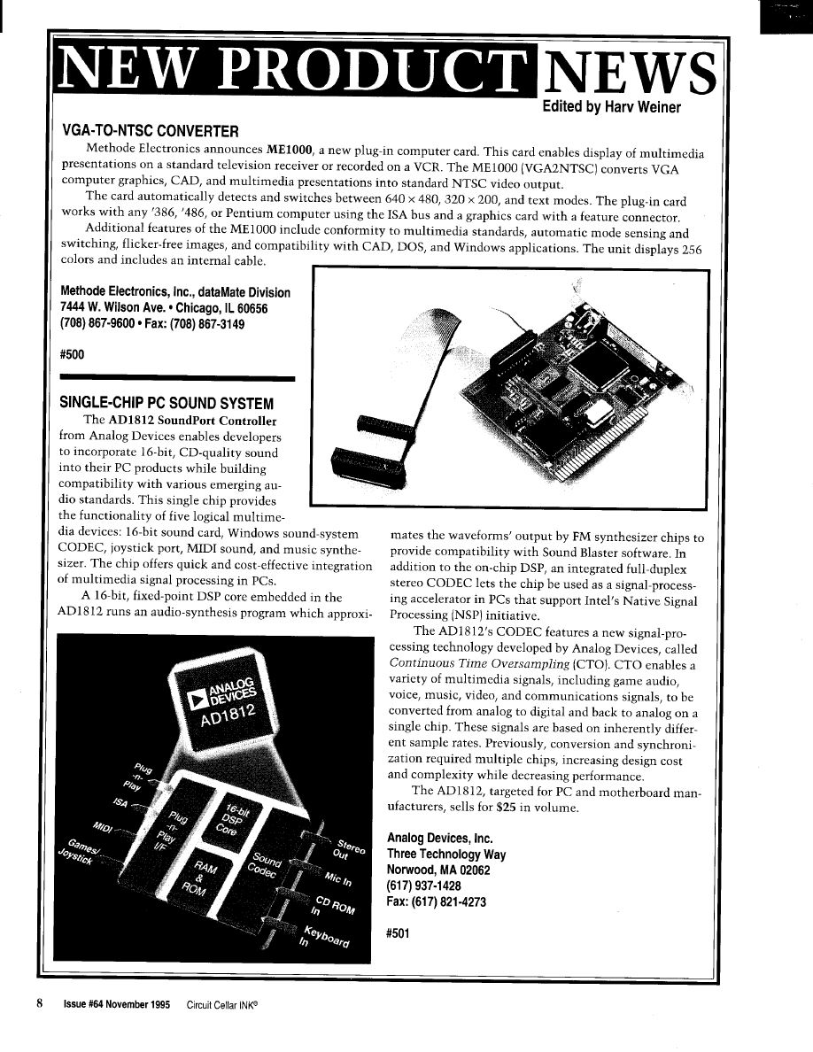
GTEK announces the
a
RS-232C interface, and compatibility with all the
speed communications card that lets a seven-node BBS
lar BBS software that supports the FOSSIL command set.
run along with
service. Additional cards
The Guardian watchdog circuit constantly monitors
provide even more nodes on the same PC.
the computer. If a problem results in a lock-up, the
has 128 KB of
buffer. Along with its
built-in FOSSIL support,
the card handles the
normal load of a BBS and
the continuous stream of
data from a C- or
band satellite receiver.
is transparent
to
soft-
ware and requires no
special drivers.
Standard features
include eight high-speed
communications channel
FOSSIL driver and
Guardian hardware auto.
resets the corn
puter, enabling system
operation in a
away, lights-out environ
ment.
Installation is sim-
ple. The user inserts the
card in the PC, config-
ures the BBS software to
work with FOSSIL, and
sets up
The
then take;
over all communication,
for
GTEK, Inc.
buffers (resulting in 43 KB more space for each BBS
node), data rates up to 115,200 bps, full ten-conductor
399 Highway 90
l
Bay St. Louis, MS 39521
(601) 467-8048
l
Fax: (601)
LIGHT-TO-FREQUENCY CONVERTER
Texas Instruments introduces two new light-to-frequency converters. The TSL235 is ideally designed for por-
table applications such as cameras, hand-held diagnostic equipment, and light meters. The TSL245 infrared (IR) con-
verter
is ideal for applications such as paper detection, proximity detection, and diagnostic equipment. Both devices
directly convert light intensity to a high-resolution digital format.
Interfacing directly to a microcontroller or DSP, the
and TSL245 combine a photodiode and
frequency converter on a single chip. Both devices provide a simple way to process a wide dynamic range of light
levels without external signal-conditioning circuitry or A/D converters.
The chips feature light-to-digital conversion with a pulse-train output, a dynamic range of 120
with
full-scale output, a voltage operation of 2.7-5 VDC, and a TTL-compatible output with frequency directly propor-
tional to light intensity on the photodiode.
The TSL235 and TSL245 sell for $1.75 in 1000 quantity.
Texas Instruments, Inc.
Semiconductor Group
SC-95044
Literature Response Center
P.O. Box 172228
Denver, CO 80217
(800) 477-8924, Ext. 4500
Conventional light
system
S
Circuit Cellar
Issue
November 1995
MULTIFUNCTION WATCHDOG TIMER
Industrial Computer Source introduces
a cost-effective multifunction watchdog timer card that
includes a number of diagnostic functions relative to the
host PC in which it resides. The
offers the
host computer excellent protection from temporary mal-
functions.
In the event of a processor failure, program glitch,
electrical noise, or compo-
nent failure, a relay output
and/or reset-line output
may be used to reset the
computer if reset does not
occur through the user’s
application program. Time-
out periods are software
selectable from 10 ms to 80
min.
The
aug-
ments its watchdog func-
tion with a number of
internal host-computer
diagnostics, including a
voltage monitor which verifies that all four computer
voltages are within 7% of nominal, a temperature alarm
that activates if the unit exceeds 50°C (adjustable), tem-
perature monitor that can be read to within
watchdog timeout buzzer, fan-speed detector that trig-
gers if fan-tachometer output drops below 50 Hz, and
two isolated input and output lines for interrupts and
computer reset.
The
sells
for $195 and includes diag-
nostics, software, and
manual. Model
a basic version without the
diagnostics, sells for $125.
Industrial Computer Source
9950 Barnes Canyon Rd.
San Diego, CA 92121-2720
(619)
Fax: (619) 677-0895
Circuit Cellar
Issue
November 1995
11
BATTERY-PACK TEMPERATURE MONITOR
Dallas Semiconductor introduces DS2434, a battery identification chip which monitors and reports battery tem-
perature and charge status in portable electronics, hand-held instruments, and medical devices. The DS2434 is a
digital-output temperature sensor that senses battery temperatures on-chip, eliminating the need for thermistors.
The DS2434 provides a convenient method of tagging and identifying battery packs by manufacturer, chemistry,
or other identifying parameters. It stores battery-charge parameters, recharge history, and charge and discharge char-
acteristics in its expanded
nonvolatile memory. Battery-pack temperature is monitored and reported digitally.
Battery manufacturers can assign an
identification number to battery
packs to aid in maintaining warranty
information.
The expanded memory of the
DS2434 offers sufficient storage ca-
pacity for user data such as gas gauge
and manufacturing information and
battery history. Information is sent
and received via a one-wire interface
so that the battery packs only need
three output connections: power,
ground, and the one-wire interface.
The DS2434 sells for $2.98 in
1000 quantity.
Dallas Semiconductor Corp.
4401 South
Pkwy.
Dallas, TX 75244-3292
(214) 450-0448
Fax: (214) 450-0470
PCMCIA READER/WRITER
Greystone Peripherals has introduced the GS-220F
a
floppy combo that accommodates two PC
card Types I, II, and/or III as well as a
half-height
floppy disk drive in a single 5.25” drive bay on a desktop
PC. The unit accommodates PCMCIA devices up to
15
mm and includes a patented eject mechanism,
panel telephone jack, and convenient plug-and-play in-
stallation.
The two-socket
floppy combo offers easy
plug and play of, any memory and I/O PC cards designed
to PCMCIA specifications. The
is a totally
compatible solution for reading and writing data or for
exchanging data files and peripheral I/O functions be-
tween mobile and desktop PCs using PC cards.
software supports most flash-file software
systems, which are provided with various flash cards,
and protects critical data integrity, so PC cards can be
moved from system to system and slot to slot.
software also manages system resources. It includes
DOS- and Windows-compatible PCMCIA card and
socket services software for configuring the system and
each PC card. It also manages I/O ports, interrupt levels,
and memory blocks. The software offers online PC card
insertion and removal, an important feature for preserv-
ing data integrity and preventing data loss.
Each turnkey
includes the two-slot dock-
ing bay hardware, a PC interface card [installs into any
16-bit AT-bus slot), cables, and software. The
is easy to install and use and features LED read/write
activity indicators.
Greystone Peripherals, Inc.
130A Knowles Dr.
l
Los Gatos, CA 95030
(408) 866-4739
l
Fax: (408) 866-8328
12
Issue
November 1995
Circuit Cellar
FEATURES
Rediscovering
Analog Computers
Parallel Processing
with Transputers
Developing a Virtual
Hardware Device
Developing an
Engine Control System
Rediscovering
Analog
Computers
Do-While Jones
hen digital
microcontrollers
are on a chip, why
would you use an analog
computer?
Well..
there’s still one
thing that analog computers do better
than digital computers-they solve
differential equations.
And, since you can build an analog
computer using just a few chips at a
cost comparable to a microcontroller,
there are times when an analog solu-
tion makes sense.
I
rediscovered analog computers
when I was writing “Cruising with
Ada”
which demonstrated how to
use Ada as an executable program
design language. I illustrated my tech-
nique by designing an automobile
cruise control. In the course of the
article, I showed how to develop and
test the cruise-control algorithm in
Ada before translating the resulting
program into assembly language for a
microcontroller.
One of the points I wanted to
make was that each project requires
you to write a lot of support software.
You need to take that into account
when planning the project. In this
particular case, the support software
was a simulated automobile that test-
ed how well the cruise control worked.
It took more lines of code to simulate
the automobile than it did to imple-
ment the cruise-control algorithm (i.e.,
it proved my pointed exactly).
Although I didn’t say so in that
article, I could have used an analog
computer to simulate the automobile.
An analog computer would have of-
fered a more accurate simulation and
would have been quicker to design and
1 4
Issue
November 1995
Circuit Cellar INK@
build. As well, I could have used the
same analog computer to test both the
Ada prototype and the microcontroller
product. It would have let me verify
the equivalence of two designs.
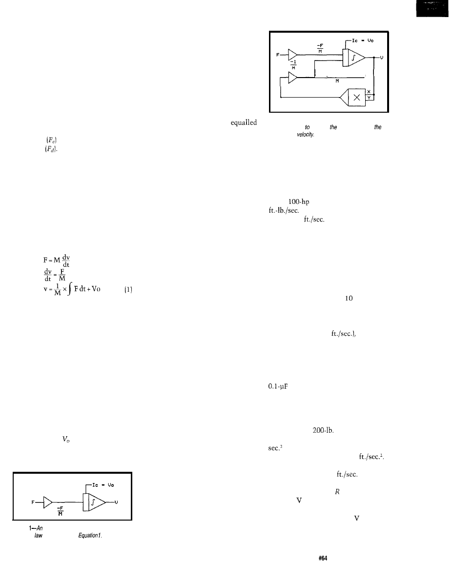
AN ANALOG EXAMPLE
The movement of an automobile
body is determined by Newton’s fa-
mous law: F = MA, where F is the total
force acting on the body. In a simple
simulation, F is the force applied by
the engine
less the aerodynamic
drag force
M is the mass of the
body, which can be determined from
the weight of the vehicle. A is the
resulting acceleration of the body.
But, I really don’t care about the
acceleration. I want to know the veloc-
ity of the body because I am trying to
control its speed. Since acceleration is
the derivative of velocity, I can rewrite
Newton’s equation and solve for veloc-
ity:
F = M A
So, to find the velocity, you have to
integrate force with respect to time.
Figure 1 shows how to do this
with an analog computer. A voltage
representing the force applied to the
body is multiplied by an inverting
amplifier with a gain that represents
the mass of the body. The resulting
voltage represents -F/M. This voltage
is applied to the input of an inverting
integrator, which produces an output
voltage that represents velocity. To
give it the proper initial condition [i.e.,
the proper initial velocity), the inte-
grator has an input that holds the out-
put at the value until time = 0.
This crude model of an automo-
bile was inadequate for my purpose.
Figure
amplifier and an integrator solve
Newton’s
as expressed in
Even the smallest engine eventually
moves the car at an infinite velocity,
which isn’t very realistic. So, I added a
simple drag model.
I
ignored friction
and viscous drag, and assumed that all
drag would be due to pressure drag,
which is proportional to the square of
the velocity. I assumed a top speed for
the car, calculated the force the engine
could produce at that speed, and
picked a drag coefficient that
the engine force at top speed.
Figure 2 shows how drag can be
added to the analog computer program.
The velocity is applied to both the x
and y inputs of an inverting xy multi-
plier, resulting in a voltage that repre-
sents the velocity squared.
To convert force to acceleration,
the velocity squared has to be multi-
plied by a gain factor that represents
the drag coefficient, and divided by a
gain factor that represents the car’s
mass. Both of these gain factors can be
combined in a single inverting ampli-
fier. The drag acceleration has an oppo-
site polarity of the engine acceleration,
so the integrator combines the differ-
ence between the two accelerations to
determine the output velocity.
This is such a simple program that
one doesn’t really need an expensive
analog computer for it. No doubt, you
could build it using an op-amp and an
analog-multiplier chip. I’ll bet you
would use something that looks a lot
like Figure 3.
If the program didn’t have the drag
(feedback) path, you would have to do
something to keep the capacitor from
integrating the input-offset voltage.
But, since there is some negative feed-
back, you don’t need to include the
initial condition input. The output V
goes to 0 in a few seconds if F is kept
at zero.
SCALING VOLTAGES IS TRICKY
Conceptually, this is a very simple
program [or circuit). Determining the
scale factors is the only tricky thing.
The scale factors have to be chosen so
their voltages don’t exceed the supply
voltages or be so small that they get
lost in the noise. Furthermore, the
time scale is a function of the ampli-
tude scale factors. Skill is required to
pick the scale factors.
D r a g c o e f f i c i e n t
- V e l o c i t y s q u a r e d
Figure 2-An analog computer program uses an
analog multiplier compute effect of drag on
automobile’s
To make it simple, ignore the drag
portion of the circuit for a moment
and consider just the portion of the
analog computer shown in Figure 4.
First, you need to know the range of
values of the input force.
A
engine produces 54990
of power (i.e., 470 lb. of
force at
117
or 80 MPH or 4,700
lb. of force at 8 MPH). Although theo-
retically it can produce 47,000 lb. of
force at 0.8 MPH and infinite force
when stopped, I am most interested in
the performance of the cruise control
when the speed is 40-80 MPH and the
engine is producing 470-940 lb. of
force.
So, if 1000 lb. equals V and we
are using a 15-V power supply, the
engine force is limited to 1,500 lb. at
low speeds. Similarly, if
10
V repre-
sents 100 MPH (146
the sup-
ply voltage limits the car to 150 MPH.
Both values should be acceptable.
In Figure 4, I need to pick resistor
and capacitor values which correspond
with these scale factors. If I pick a
capacitor just because I have a
drawer full of them, what’s my value
for R?
If I apply a constant 1000 lb. of
force to a car that weighs 2752 lb.
(including the
driver), the mass
of 2752 lb. is 2752 divided by 32.2 ft./
or 85.47 slugs. My acceleration is
1000 divided by 85.47 or 11.7
So, after 10 sec. of acceleration, the car
will be moving at 117
or 80
MPH.
I want a value of so that if I
apply 10 (1000 pounds of force) to
the input of Figure 4 for 10 s, the volt-
age across the capacitor is 8 (80
MPH). The well-known equation for
voltage across a capacitor is:
Circuit Cellar INK@
Issue
November 1995
1 5
i d t
Since the current is a constant
(10
V
I can pull the value out of the
integral:
R=
Since that’s a larger resistor than I’m
comfortable with, I’ll let = 1.25
and C = 10
There is another way to make the
component values more reasonable. If I
scale the input so that 1 V = 1,000 lb.
of force (instead of 10 V = 1,000 lb. of
force), then can equal 1.25
and
C is 1
The normal input voltage
then is 0.47-0.94 (rather than 4.7-9.4
V), which is well above the noise level.
I could even let 1 V = 100 lb. of force,
let
R =
125
and C = 1
The input
voltage at cruising speeds would be
47-94
It’s difficult to select reasonable
values for the capacitor, resistor, and
voltage because the simulation has to
run in real time. If I weren’t restricted
that way, I could let 10 V = 1,000 lb.,
R =
125
and C = 0.1
The simu-
lation would run 1000 times faster
than real time, the capacitor would
charge up to 80 MPH in
of the
time, and I could display the voltages
on an oscilloscope and interpret milli-
seconds as if they were seconds.
Ironically, it is sometimes difficult
to get digital simulations to run fast
enough for real time, but with analog
simulations, the problem is getting
them to run
slow
enough. If you pick
reasonable voltages and resistances,
the capacitor values often have to be
very large. It can be difficult (and ex-
pensive) to find precision large-value
bipolar capacitors with low leakage.
(Leakage decreases the voltage across
the capacitor, giving erroneous an-
swers.)
If you pick reasonable voltages and
capacitors, then the resistors often are
very large. This problem leads to stray
capacitance, leakage through dirt and
condensation on the circuit board, and
errors due to op-amp input-bias cur-
rent and input-offset current.
If you pick reasonable resistors
and capacitors, then the voltage levels
have to be very small. You then have
trouble with noise and DC offset.
I’ve been out of analog-circuit
design for about 20 years, but I assume
analog components have improved as
much as digital components have.
There must be op-amps today that
have less noise and input current than
the old Fairchild 741 had. Building an
integrator that accurately simulates an
automobile body in real time shouldn’t
be as hard with today’s components as
it was 20 years ago. But, with proper
scaling, I could even use a 741 op-amp
and still get results good enough for a
real-time automobile simulator.
FINDING THE MISSING INPUT
The input to this analog computer
is the force applied to the automobile
body by the engine. However, the
output from the cruise control is a
throttle setting. How do you convert
throttle setting to engine force?
Since this was a quick-and-dirty
model to prove a concept, I assumed
that engine power (not force) is lin-
early proportional to the throttle set-
ting. This is almost certainly not true,
but I’m not an automotive engineer so
don’t know what the relationship is.
It is more likely a curve with nas-
ty discontinuities when the transmis-
sion shifts gears. However, over the
cruising range, when the transmission
stays in one gear, a linear
Figure
analog computer
program from Figure 2 can be
built from two op-amps and an
analog multiplier.
RELAY INTERFACE
. . . . . . . . . . .
Two 8 channel
outputs are
to relay cards
for
using
EX-16
AN.2
INTER ACE (2
10 am
REED RELAY CARD
. . . . .
RELAY CARD (10
‘ANALOG
( C
O N N E C
TS
ADC-16
CONVERTER’ (16
AID CONVERTER’ (8
Input
amperage. pressure, energy usage.
joysticks and a wide
of other types of analog
signals.
available (lengths to
Call for info on other
configurations and 12 bii
converters (terminal block and cable sold separately).
TEMPERATURE INTERFACE’ (8
Includes term. block 8 temp. sensors (-40’ to 146’ F).
STA-8 DIGITAL INTERFACE’@
Input on/off status of relays, switches, HVAC equipment,
security devices, smoke detectors, and other devices.
TOUCH TONE INTERFACE’................ 134.90
Allows callers to select control functions from any phone.
PORT SELECTOR (4 channels
Converts an
into 4 selectable RS-422 ports.
CO-485 (AS-232 to
l
EXPANDABLE...expand your interface to control and
monitor up to 512 relays, up to 576 digital inputs, up to
128 analog
or up to 126 temperature inputs using
the PS-4. EX-16, ST-32
expansion cards
FULL TECHNICAL
over the
telephone by our staff. Technical reference disk
including test
programming examples in
C and assembly are provided
each order.
HIGH
for
24
hour industrial
with 10 years of proven
performance in the energy management field.
CONNECTS TO RS-232,
or
with
IBM and compatibles, Mac and most computers. All
standard baud rates and protocols (50 to 19,200 baud).
Use our 800 number to order FREE INFORMATION
PACKET. Technical Information (614) 464.4470.
24 HOUR ORDER LINE (800) 842-7714
Visa-Mastercard-Amencan Express-COD
Domestic FAX (614)
Use for Information, technical support orders.
ELECTRONIC ENERGY CONTROL, INC.
360 South
Street,
604
Columbus, Ohio 43215.5438
Circuit Cellar
Issue
November 1995
1 7
tion is probably good enough. [If it’s
not good enough, a look-up table in
the cruise-control algorithm can
compensate for the curve and make
it linear.) So, I assume the cruise
control output is power.
Force is power divided by veloc-
ity. However, analog-division cir-
cuits are much less common than
analog multipliers. A multiplier does
division by putting it in a feedback
loop.
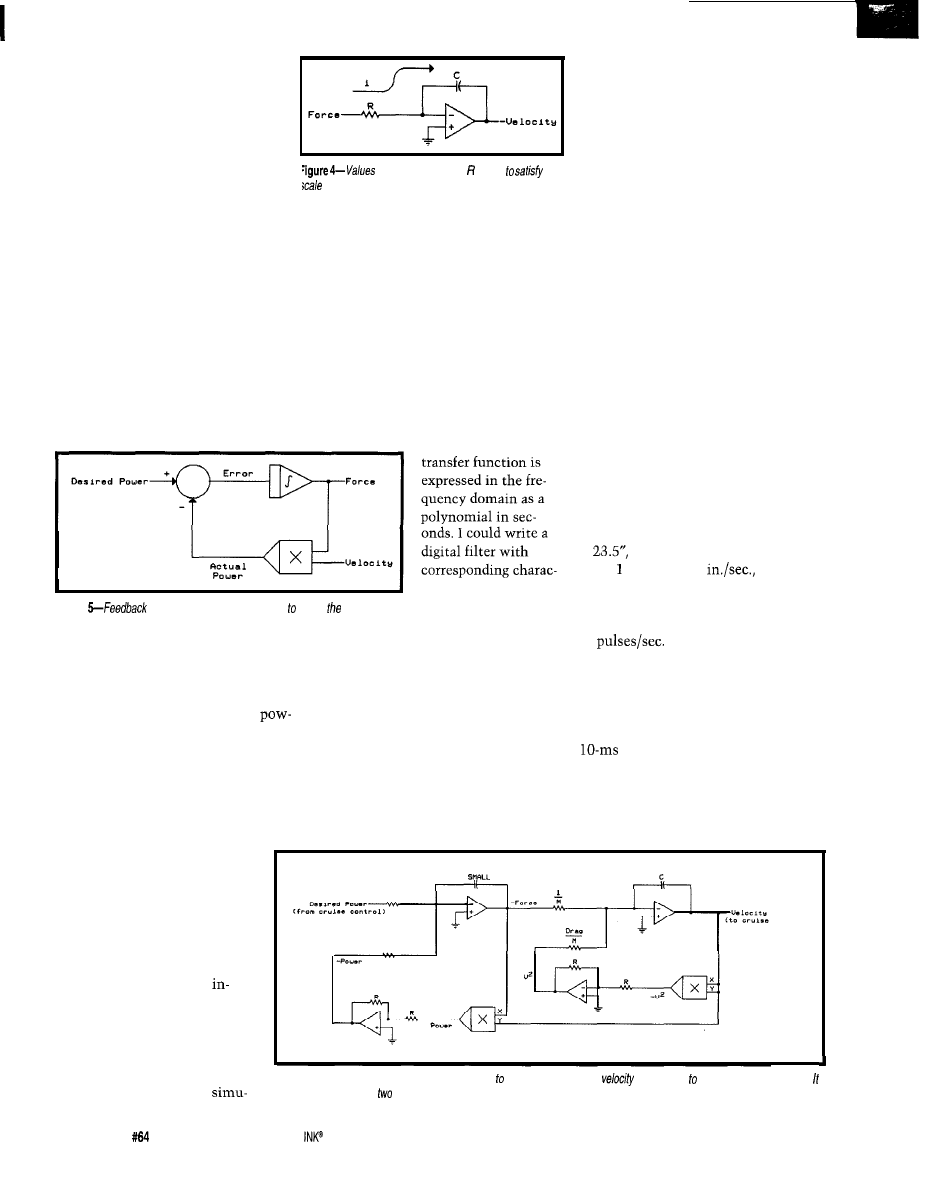
In Figure 5, I assume that the force
voltage comes from a magic, unknown
source (which I will create later). I
apply force and velocity to the two
inputs of an inverting analog multi-
plier. Since the product of force and
velocity is power, the output of the
inverting-multiplier circuit represents
negative power.
must be chosen for and C
the
factors being used.
lator using two op-amps and two ana-
log multipliers instead of simulating it
in software. Figure 6’s crude analog
computer is no worse than the digital
simulation, which uses the same sim-
plifying assumptions (i.e., drag is pro-
portional to velocity, and power is
proportional to throttle position), but
was good enough for proof of concept.
If I need to have a better model, I
must measure the transfer functions of
the components of the body. When I
do this, the open-loop
teristics [see “Digital
Figure
determines fhe force necessary create desired
Filter Alchemy,” INK
power.
61) and put it in the
digital simulation.
I put the negative power into a
But, it would be just as easy, if not
summing junction that combines it
easier, to design an active analog filter
with the desired power input. If the
with the same transfer function.
power exactly equals the desired
In general, as the requirements for
er, they cancel each other. As long as
a simulation become more severe, the
there’s no error, the integrator holds
digital solution gets more difficult at a
the force at the same correct value.
faster rate than the analog solution
If the power and desired power
does. This was particularly true in the
don’t exactly cancel each other out, an
cruise control example because of the
error voltage is produced. This error is
time-frequency problem.
applied to an integrator, which
is the magic source for the
force. (Use a small capacitor in
this integrator so it’s much
faster than the rest of the time
constants and doesn’t affect the
response of the circuit.) As it
turns out, the polarity of the
error is backwards, so an
verter has to be added before or
after the integrator.
Suppose you measure speed by
putting a magnet on one of the axles
and using a sensor that produces one
pulse per wheel revolution. The out-
side diameter of the tires on my truck
is
so the circumference is 73.8”.
Since MPH is 17.6
a vehicle
moving 1 MPH produces 0.238 pulses/
sec. If the cruise control is specified to
work from 40 to 80 MPH, there’s 9.5-
19
I designed the control loop to
measure speed every 100 ms. (I picked
this value because I know guided mis-
siles, which go 10 times faster than an
automobile, can be controlled with a
cycle-control loop.)
During the sample period, 80
MPH produces
1.9
pulses, which isn’t
a very useful measurement of speed!
Even if you increase the sample period
Figure 6 shows how this
inverter can be added to the
circuit in Figure 3. I could have
built a crude automobile
Figure 6-An analog computer circuit can be used compute automobile
in response cruise control commands.
uses four op-amps and inverting xy multipliers.
THE TIME-FREQUENCY PROBLEM
In “Cruising with Ada,” one of
the points I make is that software
projects don’t fail because of too much
coupling, too little cohesion, improper
indentation, or other things computer
scientists worry about. It’s true: bad
software engineering practices do in-
crease the number of defects, develop-
ment time, and maintenance costs, so
should be avoided. But, crummy code
doesn’t usually cause project failure.
A project usually fails because a
fundamental problem isn’t discovered
until operational testing, which is
generally at the end of the project. I
encourage rapid prototyping because
the sooner you get something opera-
tional, the earlier you discover the
killer problem. In the cruise control,
the problem was the time-frequency
uncertainty principle.
18
Issue
November 1995
Circuit Cellar
to 200 ms, you only get
1,
2, or 3 puls-
es during the sample period, which
translates to
21, 42,
or
63
MPH. The
control loop can’t possibly give satis-
factory performance with such a coarse
measurement.
You can measure average speed
more accurately if you count the num-
ber of pulses in a 10-s period. Then,
130 pulses corresponds to 54.5 MPH,
131 pulses to 55.0 MPH, and 132 puls-
es to 55.5 MPH. Although this gives
the average speed to
resolu-
tion, there is some uncertainty about
the instantaneous speed. The control
loop is likely to be unstable because
vehicle speed changes too much in a
period. The trick in getting a
cruise-control solution is to make the
proper tradeoffs between measuring
speed quickly and accurately.
I’m sure you can think of several
different ways you might do this (e.g.,
add more magnets, use the pulses to
gate a high-frequency oscillator, etc.).
Whatever you do, you have to simulate
it accurately because it is critical to
the performance of the cruise control.
I didn’t carry the example any
further in “Cruising with Ada” be-
cause of the difficulty of simulating an
FM-modulated pulse train on a digital
computer. With digital, the period of
the modulation frequency can be less
than the computational cycle of the
cruise control. To convince myself
that I had correctly simulated the
response of the speed-sensing circuit,
it would have required a lot of testing.
But, if I had used an analog com-
puter, it would have been trivial. It
would take most of you less than an
afternoon to design a linear
controlled oscillator that produces 9.5
pulses per second when the input volt-
age is 4.0 V (40 MPH) and 19 pulses per
second when the input is 8.0 V.
Several hours later, Edison asked
what the volume was. The assistant
showed him sketches of the bulb’s
outline, the function used to approxi-
mate the outline, and several pages of
calculus used to find the volume of a
solid of revolution by parts.
Without saying a word, Edison
picked up the bulb, walked to the sink,
filled the bulb with water, and dumped
it into a measuring cup.
Obviously, a measuring cup does
not
eliminates the need for calculus. It
simply illustrates how we can over-
look simple solutions because we’re
accustomed to using the difficult ones.
Similarly, I’m not saying analog
computers eliminate the need for digi-
tal computers. I just want to point out
that the analog computer is a useful
tool often neglected today. Many
younger engineers assume they are
obsolete.
So, it is worthwhile to remind
everyone that the analog computer is
still viable. It is a measuring cup that
sometimes gives you the answer faster
and more accurately than modern
methods.
For problems that are difficult on a
digital computer, especially if it in-
volves differential equations or an
analog simulation, consider using a
general-purpose analog computer (or
build a circuit that is a special-purpose
analog computer). An analog solution
could save you months of design time
and give you more accurate results.
Do- While [ones has been employed in
the defense industry since 1971. He
has published more than articles in
a variety of popular computer maga-
zines and has authored the book Ada
in Action. He may be reached at
DON’T OVERLOOK THE SIMPLE
once heard a story about an inci-
dent that allegedly happened in Tho-
mas Edison’s research lab. The story
may not be true, but its moral is.
Edison was improving his
bulb design by trying different fila-
ments, gases, and shaped bulbs. He
asked his assistant to find the volume
of an odd-shaped blown-glass bulb.
Do-While Jones, “Cruising with
Ada,” Embedded Systems
Programming, 1994.
401 Very Useful
402
Moderately Useful
403 Not Useful
STORES!
P U T
Circuit Cellar
TO WORK
FOR YOU!
Circuit Cellar INK
readers are
engineers, programmers,
consultants, and serious
outer technologists. Bring
them into your store by selling
Circuit Cellar INK.
Circuit Cellar
Direct Dealer
Sales Program lets you increase
your store traffic, increase your
sales, and increase your profits
with minimal risk and up-front
investment.
For information on how your
business can become part of
the growing
Circuit Cellar INK
success story, write or call:
Circuit
Cellar INK
Dealer Sales Program
4
Circuit Cellar INK@
November 1995
19
David Prutchi
Parallel Processing
with
Transputers
hen John Von
Neuman estab-
lished the basics for
sequential computer
architectures in 1947, he simplified his
solution to its very basics-a series of
primitive numeric manipulations
executed on data stored in a memory
system. Each manipulation was carried
out, one at a time, by a centralized
processor. Since then, major improve-
ments in computational throughput
have been achieved by using more
ample instruction sets with wider data
and address buses and by increasing
system clock speed.
However, little can be done to
speed up a system already running at
full tilt. Current clock speeds border-
ing on 200 MHz already present diffi-
cult design and layout problems that
heavily affect a system’s flexibility,
performance, and price. Further in-
creases in clock speed may require
sophisticated semiconductor materials
(e.g., gallium-arsenide) and specialized
interconnection technologies with
prohibitive costs.
Ultimately, even if all other issues
are solved, uniprocessor machines are
limited by signals that can’t travel
faster than the speed of light across the
finite dimensions of the processor.
Using multiple processors, tightly
or loosely coupled, to share the work-
load achieves higher computational
power without raw increases in speed.
This strategy, called parallelism, can
be exploited in three ways:
l
Algorithmic-the algorithm is bro-
ken down into a pipeline of multiple
processes
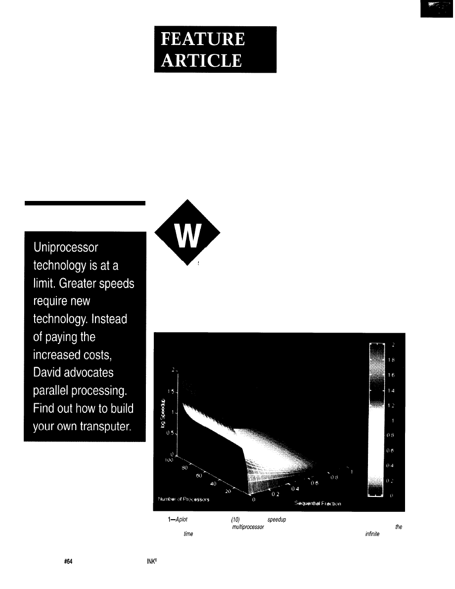
Photo
of the
logarithmic maximum
that can be achieved through an idea/ parallel computer
demonstrafes that effective use of a
machine can only be achieved through a drastic reduction in
percentage of
spent executing sequential code. For large sequential fraction values, even an
number of
processors on/y achieves modest performance improvements.
20
Issue
November 1995
Circuit Cellar
scheduler and FPU
J7
and analysis
System
control
logic
PC bus
l
Geometric-the problem is broken
down into a number of similar pro-
cesses, each with a different subset
of the total data to be processed. The
processes communicate as they need
access to data assigned to another
process.
l
Farming-the workload is “farmed
out” by a master controller to other
computing servers. The master dis-
penses new work to the servers as
they become free.
Farming automatically balances
the workload among the network serv-
ers regardless of network topology. It is
limited only by the rate work can be
dispensed and results handled. Unfor-
tunately, farming is effective only
when the problem can be divided into
small, similar pieces, which represents
only a small portion of the work de-
manded from a general-purpose com-
puter.
Geometric parallelism introduces
a major system design difference be-
tween Von Neuman sequential prob-
lem solving and parallel computation,
namely the topology of the parallel
processors’ network. In principle, the
processors need to be connected in
such a way that the network topology
somehow models the structures inher-
ent to the problem. If a good model is
found, the partitioning of the algo-
rithm is simple to understand and
implement.
Parallel machines based on spe-
cialized
have been developed ex-
perimentally for more than a decade. A
number of parallel-processing com-
puters and supercomputers are avail-
able, but only for large budgets. Lately,
however, parallel processing
have been designed that may launch
the personal computer into affordable
desktop supercomputing.
Intel and others offer parallel pro-
cessing boards with a small number of
scalable-architecture processors, such
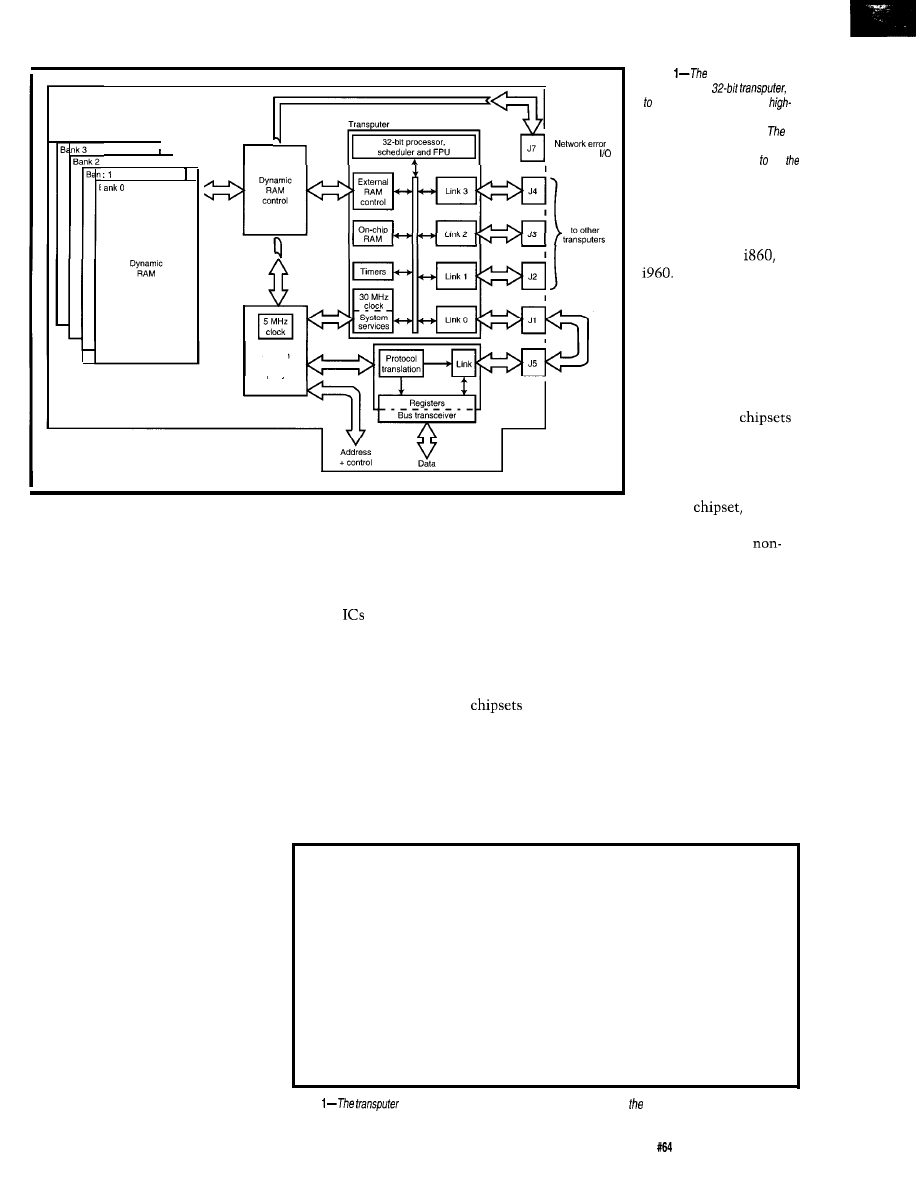
Figure
PC add-in transputer
card features a
up
4 MB of DRAM, and three
speed /inks for connecting to an
external transputer network.
card a/so offers a hierarchical
network analysis structure aid
development of multitransputer
systems.
as
the Pentium,
or
By sharing system
resources, these pro-
cessors achieve perfor-
mances in the hundreds
of MIPS range. At the
same time, companies
such as Chips and Tech-
nologies are introducing
multiprocessor
that address many of the
hardware design issues
for shared-memory mul-
tiprocessor systems. The
CS8239
for
instance, interconnects up to six ‘486
microprocessors to a fast, wide,
multiplexed bus that permits multiple
masters.
Most of these efforts are inher-
ently limited because bus-based,
shared-memory computers (regardless
of the number of processors they use)
are limited in practical scalability by
memory contention and bus band-
width. Implementing distributed
memory systems instead of shared
memory schemes avoids most scalabil-
ity limitations. However, processors
with distributed memories require
communication to effectively exploit
geometric parallelism. This shift in the
Iptr-This instruction pointer acts as a conventional program counter. It points to the
next instruction to be executed.
Wptr-This workspace or stack pointer points to a storage area of local variables.
Areg, Breg, Creg-These general-purpose registers form a push-down stack (Areg on
top), so the transputer can use zero- and one-operand instructions. Because the
stack is not large enough to store variables of lengthy operations, the transputer’s
assembly-language programming usually demands extensive use of load and
store instructions, much like single-accumulator microprocessors.
Oreg-The operand register assembles the operands used by direct instructions.
Error Flag-This flag approximates a traditional overflow flag. Once triggered, how-
ever, it remains set until explicitly cleared. The state of this flag is presented to
the transputer’s Error pin, and the location of an errant transputer may be located
in a multitransputer network.
Halt-on-error Flag-When set, this flag causes the setting of the error flag to be inter-
preted as a fatal error. The whole system comes to a complete stop.
Table
has six
infernal registers and two flags which define state of a sequential process.
Circuit Cellar INK@
Issue
November 1995
21
architectural paradigm can block de-
velopment of parallel processing desk-
top supercomputers.
Already, there’s a battle to capture
the desktop supercomputer market
between Inmos (now owned by
Thomson Microelectronics) and micro-
processor industry giants. Since
Inmos has offered a transputer, which
is a microprocessor that gets its power
from the radically different philosophy
that underlies its design, although it
barely performs a la pair with Intel and
Motorola processors.
Transputers communicate with
other transputers in parallel processing
networks using minimal interconnec-
tion and communications overhead.
The same level of parallelism can be
executed on a network of devices as
within a single transputer executing
virtual concurrent processes through
ware, this article presents first-genera-
tion transputers in detail and a simple
PC add-on implementation. A brief
peek at Occam, the transputer’s native
language, is followed by a look at sec-
ond-generation transputer products
and the possibilities for desktop paral-
lel computers that can stand up to the
performance of multimillion dollar
supercomputers.
PARALLEL PROCESSING
Different approaches to the design
of parallel-processing computers have
been identified to break the process-
ing-speed limitations of sequential
architectures. Essentially, these ap-
proaches aim to overcome the
Neuman bottleneck of Single-Instruc-
tion Single-Data (SISD) computers.
Parallel architectures attempt to
gain power by performing the same
tasks to many processors in parallel
(Multiple-Instruction
MIMD). SIMD is typical for vector or
array processors while MIMD is the
basis for more flexible parallel comput-
ers because it can work efficiently over
a wide range of granularity.
There is even a hybrid of these
two architectures called Single-Pro-
gram Multiple-Data (SPMD). A copy of
the same program runs on each proces-
sor, even though the programs are not
synchronized at the instruction level.
The efficiency of each approach
may be estimated using Amdhal’s law,
a mathematical formula which as-
sumes that a computing process can be
divided into a sequential and parallel
portion Besides the parallel opera-
tions which may be distributed over a
number of processors, there remains a
sequential portion, comprising at least
hardware-scheduled sharing of the
mathematical operation on a number
the sequential communications
processor time.
of data elements simultaneously
tween the processes. The sequential
After looking at the principles of
(Single-Instruction
component limits the efficiency of a
parallel processing hardware and
SIMD) or by assigning multiple unique
parallel machine.
Figure
of the add-in card is a
or
These
transputers
host PC and other
via four high-speed bidirectional serial
The processor clock is infernally generated by a PLL oscillator locked
Processor and
speeds are selected through
bank
22
November 1995
Circuit Cellar
Under ideal conditions where no
which the hardware-676,000 gates in
overhead for communications and
52 FPGAs-is tailored through the
synchronization is required, the maxi-
software to exactly fit the algorithm.
mum
attainable by converting
Virtual Computer Corporation, the
a sequential program to a parallel im-
developers of this machine, expect
plementation is expressed by Amhdal’s
speedups well beyond those predicted
law as:
by Amdhal’s law.
=
(I)
where is the run time of the sequen-
tial version, while is that of the
parallel implementation, and is the
number of processors. is determined
by the fraction of the total time spent
executing sequential code and by the
number of available processors as de-
fined by:
In any case, Amhdal’s law conveys
the “catch” of parallel
different kinds of multiprocessing
systems suit different kinds of applica-
tions. The designer must decide what
is best for the problem at hand
As a first step, assess optimal
granularity. Although some algorithms
run more efficiently at fine-grain level
(simultaneously executing many dif-
ferent microinstructions such as move,
add, compare, write, etc.) where mul-
tiple parallel processors can be accom-
modated with ease, the organizational
overhead of communications and syn-
chronization may consume the speed
gains of parallelism.
Photo
1
displays
under
ideal conditions as a function of the
number of processors and percentage
of time spent executing sequential
code. The point is obvious-the major
enemy to
is sequential pro-
cessing. For large values of s, time loss
is so significant that an infinite num-
ber of processors only achieves modest
performance increases.
In more realistic conditions where
workload is not perfectly balanced and
communications and synchronization
requires overhead, there’s an addi-
tional toll to the theoretical
In recent years, the interpretation
of Amhdal’s law has been frequently
challenged. More conservative views
contend that Amhdal’s law applies to
all processing systems and thus de-
scribes a more general limitation on
the performance of any programmed
system above a certain level of com-
plexity. Under this view, a good se-
quential or parallel system design
should loosen the bounds imposed by
Amdhal’s law to the point where the
system becomes feasible
A more radical view disputes the
validity of Amdhal’s classical basis by
arguing that program execution time
rather than problem size is constant.
From this perspective,
is
achieved by having the software design
the hardware it needs. This idea re-
cently led to the design of a massively
reconfigurable logic computer in
However, using coarse-grain paral-
lelism (simultaneously executing sub-
routines) doesn’t ensure success. Tasks
that could be executed in parallel may
remain locked within subroutines, so
some processors remain idle for large
amounts of the computing time.
To best develop a multiprocessor
system, the designer needs to thor-
oughly understand the application and
then develop a well-structured pro-
gram that is highly modular and easy
to partition. Many engineers experi-
enced in parallel programming first
develop and debug the algorithm in a
single-task version before attempting
to deal with communications, syn-
chronization, and resource sharing.
The structured program should be
carefully analyzed to identify how to
best distribute the tasks. To achieve
the desired
optimization aims
to balance the load between parallel
processes, while reducing
tions and synchronization require-
ments. If performed correctly, this step
provides a clear view of the hardware
and software topology and the level of
granularity that best exploits parallel-
ism for your application.
The designer should also identify
how data and code distribution can be
Circuit Cellar INK@
issue
November 1995
23
Sets
the
Pace
in
CPU and DAS
Technologies
Fully Integrated PC-AT
with Virtual
Device Support
When placing your order, mention this ad
and receive a 387SX math coprocessor FREE!
200
Analog I/O Module
with Channel-Gain Table
Make your selection from:
XT,
and
processors. SSD,
DRAM,
serial ports, parallel port, IDE
floppy controllers, Quick Boot, watchdog timer, power
management, and digital control. Virtual devices
include keyboard, video, floppy, and hard disk.
7
SVGA CRT LCD, Ethernet, keypad scanning,
PCMCIA,
GPS, IDE hard disk, and floppy.
12, 14
data acquisition modules with high
speed sampling, channel-gain table (CGT), sample
buffer, versatile triggers, scan, random burst
multiburst, DMA, 4-20
loop, bit program-
mable digital
advanced digital interrupt modes,
and power-down.
&Real Time Devices USA
200 Innovation Boulevard
l
P.O. Box 906
State College, PA 16804-0906 USA
Tel:
1
(814)
Fax: 1 (814)
(814) 2351260. BBS: 1
234.9427
RTD Europa RTD Scandinavia
Budapest, Hungary
Finland
Fax: (36)
1 212.0260
Fax:
(358) 0 346.4539
RTD is a founder of the
Consortium and the
supplier of PC/l 04 CPU and DAS modules
(ProcSpeed
0
DIP
Switch
Processor Speed (MHz)
(ProcSpeed
(ProcSpeed
T400
0
0
20.0
20.0
0
0
1
0
1
0
0
1
1
0
0
1
0
1
1
0
1
1
1
22.5
22.5
25
25.0
30
30.0
35
35
Invalid
Invalid
17.5
17.5
Invalid
Invalid
Table
2-Processor-speed selection is available in discrete steps. Clock frequency is programmed through
switches
through Sl-8 up to fhe maximum rated frequency for a
device.
carried out independently. This often
results in a network which can’t be
described as a pure processor farm,
geometric array, or algorithmic pipe-
line. A simulation of a certain physical
phenomenon may have a geometric
processor array to model the physical
system, each of which feeds a pipeline
simulating a local physical process.
These in turn may own a farm of pro-
cessors which care for math operations
requiring minimal interaction.
TRANSPUTER BASICS
The transputer is a RISC computer
on a chip, complete with a high-speed
CPU, memory, external memory con-
troller, and four full-duplex communi-
cation links. Some models also include
an on-chip floating-point unit (FPU).
The transputer’s architecture achieves
optimal virtual and true concurrent
processing under Occam.
Occam enables transputers to be
described as a collection of processes
operating concurrently and communi-
cating through channels. It imple-
ments the Communicating Sequential
Processes (CSP) model of parallel com-
puting. It considers a parallel program
to be the same as a finite number of
sequential processes which execute
concurrently while exchanging mes-
sages over message channels.
As a processing unit, the trans-
puter’s integer CPU calculates address
information and presents the FPU with
data. The CPU efficiently supports the
Occam model of concurrency and
communication. A reduced number of
instructions form the transputer’s
instruction set and make concurrent
processing as efficient as possible.
A stack-based architecture uses
on-chip RAM as a conventional micro-
processor uses its registers. Concurrent
tasks map their “registers” to specific
workspace in the on-chip RAM. Table
1
describes the internal registers and
two flags which define the state of a
running process.
Switching between concurrent
tasks is as simple as switching a poin-
ter to the correct workspace. An oper-
ating-system kernel is built into the
transputer to execute multitasking
under direct hardware control. Hence,
any number of concurrent processes
can be executed together, sharing the
processor time. Hardware-controlled
scheduling eliminates the need for
external software kernels and speeds
context switching to 0.6
The hardware-process scheduler
automatically sleeps processes waiting
for channel I/O and wakes them at I/O
completion. The instruction set also
includes an Alternative command
(A LT) which makes a process dormant
until it receives an alternative en-
abling event. Two interval timers and
time-out support also keep processes
dormant until they’re needed.
Communication between concur-
rent processes takes place through
channels when both the input and the
output processes are ready. This mes-
sage-passing channel construct lets
processes share data and become syn-
chronized. Communication between
processes on the same transputer takes
place through local-memory channels.
When processes run on different trans-
puters, communication takes place
through channels implemented on the
high-speed serial links. Each link is a
24
Issue
November 1995
Circuit Cellar
fast (20-Mbps), asynchronous,
full-duplex channel.
In addition to the links,
the built-in memory control-
ler communicates with exter-
nal memory and peripherals.
The memory controller ex-
pands the address space off
chip, and can directly control
up to 4 GB of DRAM. It also
maps I/O space for interfacing
with other peripherals. Since
these modules operate
(*MemSO)-Address latch enable
address strobe
which
is selected during all memory and
access operations
notMemS2
address multiplexing
address strobe
notMemS4
used
(*MemRf)-Not used
used for memory access; used
to control the
PAL
(*MemWr)-Write control to all memory chips
Table
lines are
taneously, asynchronous communica-
tions between processes demands
minimal overhead.
TRANSPUTER SPECIES
Transputers operate with clock
rates of 15,
and 30 MHz, and
different transputer families fulfill the
requirements of different markets and
applications.
The T9000 second-generation
transputer is the latest addition to the
transputer family. This new device
sports numerous hardware enhance-
ments which increase speed and sup-
port advanced operating systems while
maintaining upward compatibility
with the
instruction set.
The
comprises a family of
transputers. These “baby trans-
puters” have 64 KB of memory space
and lack many features of their 32-bit
counterparts. Because of their low cost
(-$80 in singles for the 30-MHz mod-
el), they are especially attractive for
parallel-processing embedded applica-
tions which do not require high-preci-
sion arithmetic or extensive memory.
The
is often used as a
acquisition controller or preprocessor
within systems that use more power-
ful transputers as their main proces-
sors. As you’ll see later, integrating
other types of transputers is possible
because the internal register pointer
architecture and link protocols work
with different word lengths.
More importantly, each of the
T9000 links is connected to multiplex-
ing hardware. Communications among
processes in separate transputers takes
place along as many channels as re-
quired. Shared physical links are soft-
ware transparent. Much more flexible
parallel programs can be im-
plemented to exploit the full
power of the CSP model.
The design of the T9000
is a truly remarkable leap
beyond the
family. Its
advanced features include a
pipelined superscalar proces-
sor that delivers more than
150 MIPS and 20 MFLOPS,
on-chip high-speed cache
RAM, and
links.
However, its shortage of sili-
con and support hardware and software
have been a problem. Although the
T9000 was announced in 199 1, it only
recently started coming out of fab.
Single 20-MHz units retail at $450.
Inmos also offers a number of
interesting support
that make it
easy to design and interface flexible
transputer networks. The IMS CO12 is
an IC which converts the serial trans-
puter protocol into parallel format and
vice versa. The IMS COO4 link pro-
vides a crossbar switch between a
maximum of 32 transputer links. It is
cascadable and enables reconfiguration
The
transputer family con-
tains 32-bit microprocessors, and im-
plements all the features of the
family. However, the
has four
serial links and 4 KB of on-chip SRAM,
while the T400 has only two serial
links and 2 KB of on-chip SRAM.
The
is essentially the same
as the
family, except it has an
on-chip floating-point coprocessor.
The T800, recently replaced by the
improved
is pin-compatible with
the T425. But, with the aid of its co-
processor, it is capable of delivering
over 4.3 MFLOPS and 30 MIPS peak
30 MHz) on its own.
Circuit Cellar INK@
Issue
November 1995
25
of the transputer network’s topology
Although the BOO4 performs well
under software control.
for unsophisticated applications, the
with similar functions are
introduction of the
family made
available for the
many
products obsolete.
links, including the IMS
a
Figure 1 offers an improved circuit,
performance routing chip that
inspired by the simplicity of the BOO4
connects T9000 transputers to form a
circuit, to illustrate the design of
full-blown packet-switching network.
transputer systems. This simple
can be used in combination
circuit remains compatible with the
with any of the first-generation trans-
original B004, but also accepts the
puters by using an IMS
link
powerful members of the
family.
converter IC, which translates
Based on this figure and some help
Mbps links to the
links of
from Inmos’s transputer data book
their second-generation counterparts.
it is relatively easy to develop more
advanced systems. Figures 2-7 should
TRANSPUTER ADD-IN BOARD
enable you to build a fully functional
FOR THE IBM PC
transputer PC add-in card. Although
In 1987, Inmos introduced a T414
it’s a bare-bones approach, this design
transputer add-in board for the IBM PC
features compatibility with Inmos and
as the BOO4 model
It was developed
third-party software; up to 4 MB of
as an Occam engine hosted by the PC.
local DRAM; compatibility with T400,
In addition, it could accelerate
T414, T425, T800, and
trans-
tationally intensive tasks for the PC
puters; DIP-switch selection of
either alone or in conjunction with a
sor and link communication
transputer network. The BOO4 still
and DIP-switch memory configuration.
supports transputer didactic and
Ideally, transputer boards should
opment environments for the PC.
be constructed using four-layer PCB
technology to ensure noise-free reli-
able operation. As with every board
designed for high-speed operation,
proper impedance matching and termi-
nation, extensive power-rail and
ground-plane decoupling, as well as
path-delay equalization are required
THE
TRANSPUTER
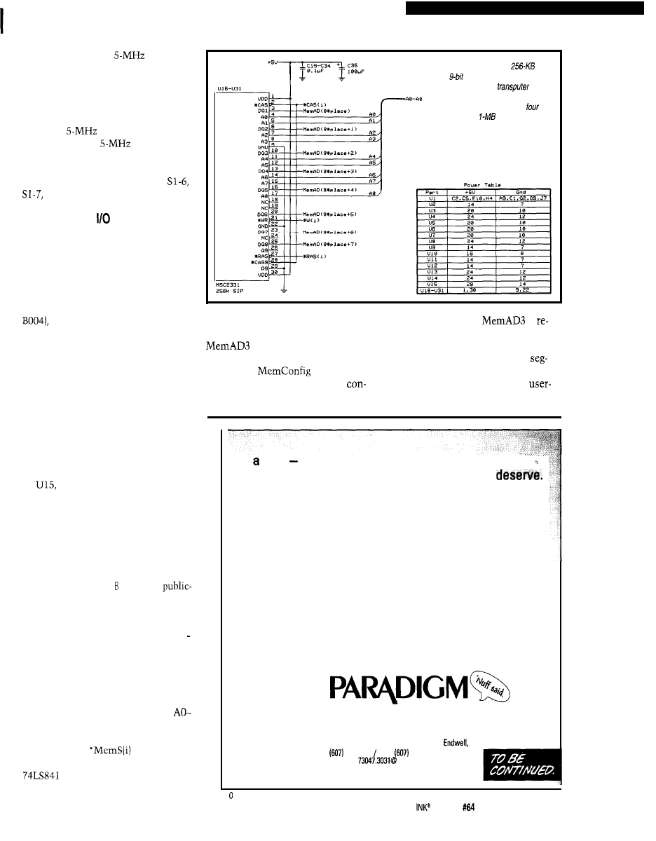
As shown in Figures 2 and 4, mul-
tiple VCC pins minimize inductance
within the IC, and all must be con-
nected to a well-decoupled power rail.
Similarly, all GND pins must be con-
nected to the board’s ground plane. C2,
a
ceramic capacitor, must be
soldered directly between
and
to appropriately decouple
the internal clock supplies. A 0.1
ceramic decoupling capacitor between
the VDD and ground planes of the PCB
should be placed near the transputer’s
socket to aid in decoupling the power
supply to this IC.
Clock design is simple since all
first-generation transputers, regardless
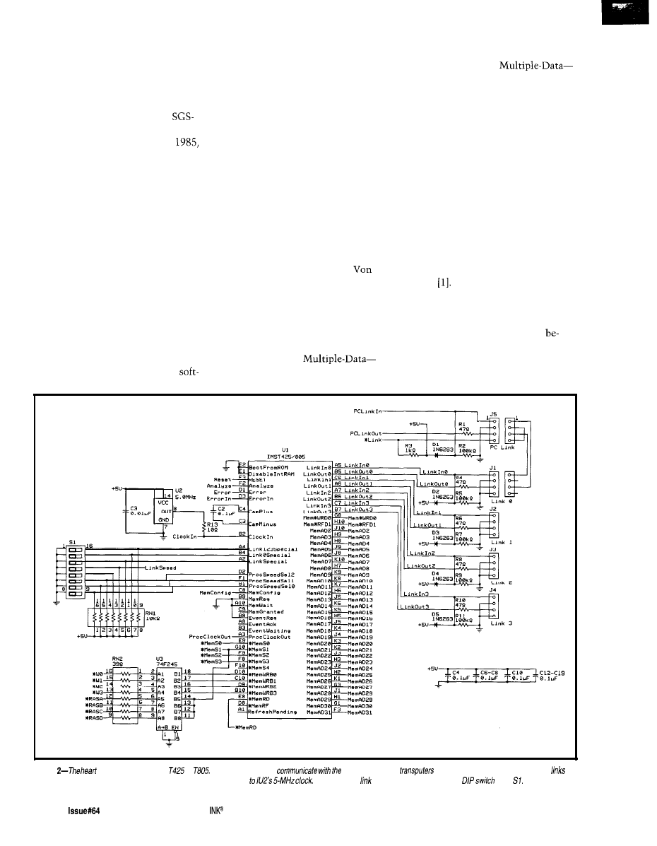
Figure
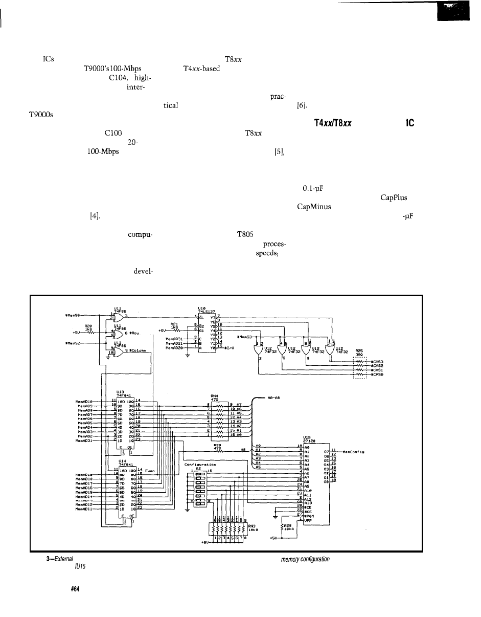
memory address and control-signal decoding is accomplished through this circuit. The actual
loaded from EPROM
info the transputer on processor reset.
26
Issue
November 1995
Circuit Cellar INK@
(strobe use, timing, etc.) is automatically
of device type, use a
clock. The
processor’s high-frequency clocks are
internally generated, which eases de-
sign and layout constraints so it’s
easier to construct a well-behaved
board.
U2, a
crystal oscillator,
produces a stable
clock signal.
Processor speed, up to the maximum
rated speed for a particular transputer,
is selected through DIP switches
and Sl-8 as shown in Table 2.
MEMORY AND SYSTEMS
The memory system implemented
in the board is capable of supporting
up to 4 MB of DRAM. This capacity is
divided among four banks of 1 MB,
each of which is implemented using
four 256 KB x 9 DRAM SIP modules.
For simplicity (unlike the original
parity-error checking has not
been implemented.
The transputer has a built-in pro-
grammable memory interface which
greatly simplifies the design of mem-
ory. This interface’s programming
determines the configuration of the
external memory cycle required for a
specific type of memory. In the board,
a configuration corresponding to a
given selection is entered through a
DIP-switch bank and is translated into
the appropriate memory configuration
by
a 27128 EPROM (see Figure 3).
A detailed explanation regarding
external transputer system memory
configuration can be found in the
transputer’s data sheet. From this, you
can configure almost every variation of
the memory system you may want to
implement in your card.
In addition, S 7 0 6 ETA, the
domain software tool used to design
the EPROM code for this add-in card,
helps you develop custom RAM con-
figurations to be loaded in U15. S7 06
BETA and PROMLOAD, another freeware
utility, help you develop bootable
EPROM code for embedded applica-
tions.
In the add-in card, the EPROM is
cycled by the decoded address bus
A5 and by the Scan/*Read line into
two corresponding phases. During the
Scan phase, all
strobes are
held logic high. This state renders both
latches transparent. When
Figure 4-Up to 16
x
DRAM modules are
available to the
as
external memory. External
memory is distributed as
banks of
x&bit DRAM.
this happens and
l
MemS2 asserts the
During the Read,
1
‘Row line, the logic high state of
mains low, selecting the EPROM’s
1
selects the EPROM’s upper
lower 8 KB. Different memory cycle
8 KB. Zeros programmed in this area
configurations are stored in 128
ensure that
is held low so
ments, each of which is 64 bytes long.
the transputer loads an external
The desired segment number is
figuration.
selected through the configuration
Be hero put Team Paradigm to work on your next
embedded x86 design and reap the rewards you
Team Paradigm has the ability to deliver all the embedded
system pieces from Intel to AMD, C/C++ or assembly
language, and all the Borland/Microsoft development toots.
Plus
Paradigm DEBUG
for your favorite in-circuit emulator
and real-time operating system.
So forget about making excuses and instead enlist
Team Paradigm for your current or next x86 project. We
deliver the finest embedded x86 development tools, backed
by unlimited free technical support. No one is more serious
about your success than Paradigm Systems. Call today
and get the details before you waste any more of your
precious time.
Proven
Solutions
for Embedded C/C++ Developers
I - 8 0 0 - 5 3 7 - 5 0 4 3
Paradigm Systems
3301 Country Club Road, Suite 2214,
NY 13760
748-5966 FAX:
748-5968
Internet:
compuserve.com
01995
Paradigm Systems, Inc. All rights reserved.
Circuit Cellar
Issue
November 1995
27
DIP-switch bank S2. The
correct memory-configu-
ration sequence results
through the cycling of
lines AO-A5. Table 3
shows how to use the
transputer strobe lines.
The transputer
system’s RAM is
mapped into negative
space. Therefore, RAM
selection occurs during
the logic-high cycles of
DIP Switch
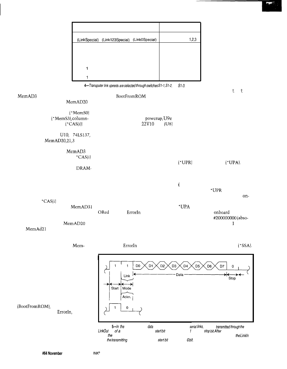
LinkSpeed(Mbps)
Sl-3
Sl-1
Sl-2
Link 0
Links
0
0
0
10
10
0
0
1
5
10
0
1
0
10
5
0
1
1
5
5
1
0
0
10
10
0
1
20
10
1
1
0
10
20
1
1
20
20
Table
and
1. Selection of the appropri-
ate bank is done through
and MemAD21. When enabled by the
address latch enable signal
and *CAS strobe
address selection signals
corresponding to each of the memory
banks are decoded by
a
which receives
1 as
inputs.
since the
line is per-
manently grounded, the transputer
waits for booting instructions to arrive
from the host PC or from other trans-
puters in a network. On
causes the logic in the
PAL
to unconditionally assert the Reset
line.
During refresh cycles,
1
is logic low, thus disabling all
lines. RAM refresh-only is implement-
ed on the board to take care of
refresh operations without disturbing
I/O.
Only the subsystem port is
mapped into the I/O area. This area
resides at a positive address, which
implies that
generation is
disabled by the logic low of
during I/O operations. I/O space is
limited to the first megabyte of posi-
tive space because both
and
have to be low for I/O
operations under the present imple-
mentation. The Even/ * Odd selection
line is the latched version of
AD2, which appears during l MemS2’s
falling edge. Figure 4 shows connec-
tion of the DRAM modules to the
decoding logic and the transputer.
The error and analysis signals aid
in developing and troubleshooting new
designs. They become especially handy
when debugging multitransputer net-
works. Asserting the Analyze line
causes the processor to halt whenever
it reaches specified breakpoint condi-
tions, complete outstanding link trans-
actions, and place special status values
on the transputer’s registers for debug-
ging.
The Error pin conveys the state of
the transputer’s internal error flag
with the
line. Internal
errors are caused by conditions such as
arithmetic overflow, divide by zero,
array-bounds violation, or through
direct software selection of the inter-
nal error flag. In a multitransputer
network, the
and Error pins of
a number of transputers
can be daisy-chained to
halt the network, mak-
ing the status of each
processor available for
probing by a master
transputer. In the trans-
puter where the error
originates, the error flag
is not cleared by a pro-
cessor Reset, so its loca-
tion can be identified.
Executing the e s e r r
instruction clears the flag and allows
for normal system operation.
The add-in board’s control signals
are mapped to the PC’s I/O space. By
doing so, the PC can reset and analyze
a network of transputers connected to
the card’s up or down subsystem ports,
This feature prevents errors in the
transputer network from flowing into
the PC, so the PC can always be ready
to reset and upload the add-in board.
Input control signals are Up-Reset
and Up-Analyze
These
signals arrive from modules of higher
hierarchy than that of the add-in trans-
puter card while Subsystem Error
l
SSE) signals arrive from modules of
lower hierarchy.
generates an
unconditional Reset signal to the
board transputer and link adapter.
signals the Analyze input. l SSE
can be read by the
transputer
at Occam address
lute address zero) as a logic in the
LSB of the word.
CONTROL SYSTEM
The transputer has a number of
incoming and outgoing system-level
control signals, which include proces-
sor reset (Reset), bootstrap control
and facilities for
error analysis (Error,
and Ana-
lyze).
The falling edge of Reset initial-
izes the transputer, triggers the mem-
ory-configuration sequence, and starts
the bootstrap routine. In this card,
Output control signals generated
by the board are Subsystem Reset
(*SSR) and Subsystem Analyze
Figure
protocol for
transmission over high-speed
each byfe
line
channel is preceded by a
and followed by a bit and a
each transmission of
a byte, sending device waifs for an acknowledge signal. This acknowledge signal, received through
line of
device, is formed by a
followed by a
28
Issue
1995
Circuit Cellar
These signals control transputers
placed in lower hierarchies than those
of the PC add-in board. Line *SSR can
be asserted by the
transputer
by writing a 1 to the LSB of absolute
address zero. Similarly,
can be
asserted by writing a 1 to the LSB of
absolute address 4
address #
20000001).
When the board is in the enhanced
mode, the PC and
transputer
can control an attached network of
transputers. To do so,
l
SSR and
l
SSA
are asserted through control signals
and
gener-
ated by the PC. This approach prevents
an error-generating network from in-
terfering with the resetting and boot-
ing of the PC’s add-in card. The status
of the
transputer Error pin is
placed in the up port as the Up-Error
signal
l
UPE.
If you want, the hierarchy arbitra-
tion can be changed by deasserting the
*System line so that an error received
from an attached transputer network
through Down-Error signal
l
DNE is
forwarded to the PC as a
and
signals received from the up
port are buffered and forwarded to the
down port as a Down Reset (*DNR)
and Down Analyze (*DNA).
The system and subsystem control
logic is implemented in US, a
PAL. The Subsystem, PC, Up and
Down Reset, Analyze, and Error sig-
nals are brought out of the add-in card
through edge connector J7 for easy
connection to an external transputer
network.
For normal operation, the *System
line must be
to ground
to
and the PC control lines must
be connected to the up port:
l
PCR to
l
UPR
to
‘PCA to
to
and
l
PCE to
l
UPE
to
AND
SERIAL LINKS
Communications through a
puter link is carried out through a
simple protocol which supports the
synchronized communication require-
ments of Occam. This protocol trans-
mits an arbitrary sequence of bytes,
which interconnects transputers with
different word lengths.
PC-Based Instruments
HUGE BUFFER
FAST SAMPLING
SCOPE AND LOGIC ANALYZER
C LIBRARY W/SOURCE AVAILABLE
POWERFUL FRONT PANEL SOFTWARE
DSO Channels
2 Ch. up to 100
Ch. at
4K or 64K
Cross Trigger with LA
125 MHz Bandwidth
Logic Analyzer Channels
Ch. up to 100 MHz
4K or 64K
Cross Trigger with DSO
$1799 DSO-28204 (4K)
$2285 DSO-28264 (64K)
PAL
GAL
EPROM
EEPROM
FLASH
MICRO
etc..
Free software updates on BBS
Powerful menu driven software
up to 128 Channels
up to 400 MHz
up to 16K Samples/Channel
Variable Threshold Levels
8 External Clocks
16 Level Triggering
Pattern Generator Option
$799 LA12100 (100 MHz, 24 Ch)
$1299 LA32200 (200 MHz, 32 Ch)
$1899 LA32400 (400 MHz, 32 Ch)
$2750 LA64400 (400 MHz, 64 Ch)
Call (201) 808-8990
Link Instruments
369
Passaic
Ave, Suite 100, Fairfield,
NJ
07004 fax: 808-8786
11
Circuit Cellar INK@
November1995
29
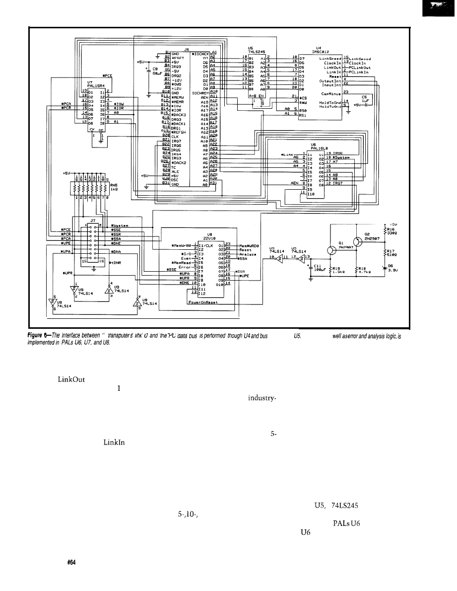
me
transceiver Glue logic, as
As shown in Figure 5, the eight
bits of each byte transmitted through a
channel’s
line are preceded by
a start bit and followed by a bit. The
data bits are then followed by a stop
bit. After each byte’s transmission, the
sending device waits for an acknowl-
edge signal from the receiving device
before proceeding. This acknowledge
signal, received through
on the
transmitting device, is formed by a
start bit followed by a 0 bit.
Transmitted bytes and acknowl-
edgments are multiplexed on the vari-
ous signal lines. As long as a process is
waiting for the sent data and there is
room in the data buffer, acknowledg-
ment is sent immediately on data
latching. The transmission is carried
out without delays between successive
data bytes.
Transputer links are designed for
electrically quiet environments. Keep
the direct interconnection between
transputers to about 1’. The link lines
are fully TTL-compatible, so
standard line drivers and receivers can
extend the distance of these links.
Interface design is simple because
all first-generation transputers use a
MHz oscillator with PLL for reference,
and no phase reference is required.
Separate transputers interconnected
through the same link may thus oper-
ate from independent clocks, each of
which may be running at a different
frequency.
Link speeds can be selected be-
tween
and 20-Mbps by pro-
gramming switches Sl-14, Sl-15, and
S 1- 16. Table 4 shows how link zero
can be set independently from links 1,
2, and 3, which must be programmed
to the same speed.
PC INTERFACE
The host PC communicates with
the transputer through one of its serial
links. As far as Occam is concerned,
this maps the PC as a process con-
nected through a channel implement-
ed on that dedicated link.
As shown in Figure 6, translation
between Inmos’s serial-link protocol
and the PC parallel data bus is per-
formed through U4, an IMS CO12 link
adapter IC. Parallel data transfers be-
tween the adapter and the PC occur
through
a
bus transceiv-
er, under the control of the logic pro-
grammed into
and U7.
and U7 decode the address bus,
data direction controls, and address/
30
Issue
November 1995
Circuit Cellar INK@
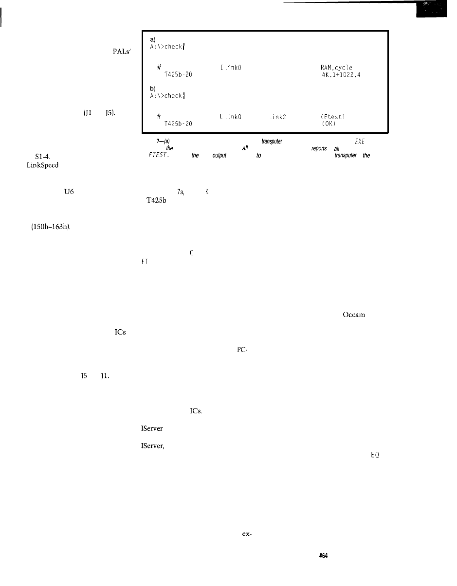
data bus demultiplexing, translating
them into an appropriate timing se-
quence for the link adapter. The
logic also arbitrates the master, slave,
and subsystem hierarchies for the
process, so Occam recognizes the PC.
Connection of the PC interface to
the transputer’s link 0 is done through
jumper cables between the PC link and
link 0 edge connectors and
Asserting *Link low enables commu-
nications with the PC bus. The link
speed for the IMS CO 12 must match
that of link 0, which is set through
switch
When this switch forces
line
low, the link adapter
IC operates at 10 Mbps. When high, it
operates at 20 Mbps.
The logic in
makes software
written for Inmos’s BOO4 compatible
with this board by placing it in the
same location in the PC’s I/O address
space
To experiment with true parallel-
ism, additional processors can be add-
ed to the transputer system. Since
additional transputers may be booted
through the serial links, only one
transputer in the network needs direct
connection to the PC bus.
In additional cards,
l
Link must be
high (achieved by removing the jumper
between pins 2 and 4 of connector J5).
Glue logic which interfaces the board
to the PC may be omitted (or the
removed from their sockets). All links
of the transputers are available for
network interconnection by removing
the connections between the PC link
and link 0 connectors and
Extra cards use the PC only as a
power source and do not need to share
the same motherboard or power
source. They may reside in an external
chassis capable of supplying appropri-
ate power and cooling or may occupy a
slot in a PC.
TESTING THE BOARD
Testing your newly assembled
transputer hardware is simple through
PC-Check, a freeware utility package
which determines the types, versions,
functionality, and topology of all trans-
puters in a network. As shown in Fig-
ure 7, PC-Check also identifies the
speed of the link connected to the
PC and performs a basic test of each
mtest
Using 150 check 3.0
Part rate Mb Bt
0
0.17 0
ftest
Using 150 check 3.0
Part rate Mb Bt
0
0.17 0
Link1
HOST
. . .
Link1
HOST
. . .
ink2
Link31
. . .
. . .
Link31
. . .
. . .
Figure
An example of a PC-Check test of the
PC add-in card shows that CHECK.
determines types, versions, and topology of transputers in a network, and
on available RAM.
(b)
EXE uses piped
from CHECK establish the functionality of each
in
transputer’s internal and external
memory.
In Figure C H EC . E X E identified
a
as connected to the host
through link 0, running at 20 MHz,
and the sole transputer in the network.
The pipe into MEMTEST. EXE reports
4 KB of 1 -cycle memory (internal
memory) and 1022 KB of 4-cycle RAM.
Piping the output of H EC K . E X E into
EST . E X E (Figure 7b) executes a full
functional test of each network trans-
puter. Each device which passes the
battery of tests receives an “OK” mes-
sage.
When C H EC K . E X E runs, it leaves
a vestigial routing trail at each node
which sets a default communications
path from the host to any transputer
in the network. Through this path,
LOAD. EXE, another program in
Check, can load programs on any
transputer node. The package also
includes a hex monitor and a simple
method for configuring the topology of
a network connected through one or
more IMS COO4 software-controlled
crossbar switch
To run your own programs, use
as an interface between the PC
host and the transputer network.
a public domain package, al-
lows the PC to reset, boot, and analyze
a transputer network. It also gives the
transputer network access to various
PC resources such as file I/O, keyboard
input, and CRT output.
OCCAM PROGRAMMING
Transputers can be programmed in
most popular programming languages,
but its special properties are best
ploited by Occam since the transputer
directly supports the Occam model of
concurrency and communication.
Occam syntax uses indentation to
indicate program structure. Specialized
folding editors are used to write a pro-
gram. A folding editor represents a
large text block in a single named fold
line marked by three dots. Folds can be
nested to any level and created before
their contents are written, allowing
the structure of a process to arise as
the design’s skeleton.
Occam describes a system as a
collection of distributed concurrent
processes that communicate with each
other through channels.
con-
sists of three primitive processes
which are combined to create larger
processes:
l
Output-c
! e
outputs expression e
into channel
c
l
Input-c? v inputs channel c into
variable v
l
Assignment-v
: =e
assigns expres-
sion e to variable v.
These primitives are joined by
three types of constructors: sequential
(SEC!), parallel (PAR), and alternate
(A LT). Statements or subprocesses
contained within the context of S
execute in sequence, while those un-
der PAR execute concurrently. In con-
trast, A LT has the processor execute
whatever component process is ready
first. Programs can be built in the
conventional way by employing vari-
ables, assignments, mathematical and
logical expressions, and with standard
constructs such as I F, WH I LE, and FOR.
Circuit Cellar INK@
Issue
November 1995
3 1
Data in
Link 1:
Link 2:
Tag + data
Tag + data + results
Link n:
Tag data + results
Link n + 1:
Results out
Data in
Results in
Results out
Data out
Results out
Figure
most simple topology
by the PAR replicator syntax is a pipeline (a). A
system is slightly more complex, using a distributor process to hand
data to concurrent worker processes, and a gatherer process collect and combine results
and output of these structures can be at one end by introducing an
additional router to achieve bidirectional communication
Each Occam channel provides a
communication element between two
concurrent processes. Information is
sent via a channel in one direction
only without message buffering. A
channel is perceived as a read-only
element to a receiving process and a
write-only element to a transmitting
process. Communication is synchro-
nized and takes place when both the
inputting and outputting processes are
ready.
The A LT construct elegantly se-
lects between executing parallel pro-
cesses. It waits for input from a group
of input channels and then executes
the process attached to whichever one
becomes active first. If more than one
input arrives simultaneously, A LT
chooses to act based on assigned pro-
cess priority and the implementation
of the program. Its choice ensures that
no channel becomes permanently
locked out.
PA R's power lies in its simple way
of replicating arrays of similar
As shown in Figure 8, the most
simple topology supported by the PAR
replicator syntax is a pipeline. Each
stage performs data processing and
passes data and/or results on behalf of
other processes.
A spaceline system is slightly
more complex. A distributor process
hands out data to concurrent worker
processes, and a gatherer collects and
combines results. In addition, since
channels are available in both direc-
tions, a router process can be intro-
duced so input and output can be at
one end of a pipeline.
and H-trees provide almost unlimited
extensibility. Two-dimensional grid
arrays are also extensible and present
improved communication and reduced
path lengths between elements. The
next level of architecture is the
dimensional cube or binary n-cube.
With
n =
2 and 3, the topology is that
of a square and a cube, respectively. A
or basic hypercube has 2’ trans-
puters and achieves an almost ideal
configuration for connectivity and
channel-path length.
The interconnection between
processes is limited only by the num-
ber of available links. While this
doesn’t pose a problem for processes
executing concurrently on a single
transputer, it does when the trans-
puter’s physical links are used as
cam channels. Then, simultaneous
connectivity between transputers is
limited to the four high-speed serial
links.
This arrangement still allows for
many useful topologies. Binary trees
A hypercube can mimic other
topologies. Processing can occur as a
number of independent trees,
or
just by preventing commu-
nications between selected nodes.
Since it is topologically identical to a
torus (an improved grid array), the
hypercube is flexible, making it a fa-
vorite architecture for multitransputer
networks.
By using multiple transputers
within a single node to extend the
number of links available to each
node, higher-order hypercubes are
32
issue
November 1995
Circuit
Cellar INK@
possible. A two-transputer supernode
has six available links and can be used
as a 6-cube. A four-transputer
node forms an g-cube, and so on.
SECOND-GENERATION
TRANSPUTERS
The T9000 second-generation
Despite a wide variety of topolo-
gies, implementation of universally
parallel algorithms isn’t possible using
transputer provides a remedy. Besides
first-generation transputer hardware
hardware enhancements that increase
and software because they comply
only partially with the CSP parallelism
operation speed and support advanced
model. The discrepancy exists because
message exchange between parallel
processes in different transputers is
operating systems, the T9000 provides
limited by the transputer’s four com-
munications links.
Communications among processes in
separate transputers takes place along
as many channels as required. Shared
physical links are transparent to soft-
ware, so true CSP parallel programs
can be used.
The new packet communications
hardware simplifies programming
because software systems then don’t
This capability is achieved
need process allocation. Different
through a separate communications
processor. It transmits messages that
allocations can be used for different
multiplex a large number of virtual
links along each physical link. Virtual
links support one
channel in
each direction. Messages are transmit-
ted as a sequence of
data pack-
ets. A header which precedes the
packet routes the packet through the
network and identifies the destination
virtual link on the remote transputer.
Moreover, the compiler can make the
allocation, removing configuration
details from the program. This is a
vital step toward development of a
general-purpose parallel computer.
To form a full-blown
switching network, one or more IMS
C 104 high-performance routing chips
interconnect T9000 transputers. Each
‘Cl04 provides 32 bidirectional
Mbps links. The header of each packet
arriving on a link input determines the
link a packet should output to as soon
as the physical link is free.
The basis for optimal packet rout-
ing is an algorithm called
interval
labeling.
An interval is a continuous
set of header values and is associated
with an output channel. The header of
an incoming packet is limited to with-
in a single range, and the packet is
directed toward the appropriate inter-
val. Most common network topologies
greater connectivity. Each link is
networks, and they can change
have stable and efficient labeling
to multiplexing hardware.
namically to optimize performance.
schemes.
Host
Host
Figure 8 (continued)-Communications between processes running in separate
(shown as dots) are limited by each
four high-speed links. Useful
topologies such as a binary free an H-free and a processor mesh can be implemented with ease. Connecting free links of fhe mesh (broken lines) results in
very powerful topology known as basic hypercube
3 4
Issue
November 1995
Circuit Cellar INK@
In the T9000, parallelism starts to
be exploited within the processor by
using a pipelined superscalar architec-
ture. The processor core executes up to
eight instructions on each
clock
cycle. Inmos even has dedicated
chip hardware which controls the flow
of multiple instructions through the
pipeline, making it possible to run
existing
code at blazing speeds.
Another improvement is the move
toward a cached architecture sup-
ported by 16 KB of on-chip cache
RAM. This much RAM is often
enough to support lightning-fast em-
bedded applications without external
RAM. The T9000 still supports exter-
nal memory through a programmable
memory interface, but it also has a
bit data bus with high data-transfer
rates for cache-line refill. In addition,
the new interface supports four inde-
pendent banks of memory, each of
which can be individually pro-
grammed.
The T9000 also provides trap han-
dling and protected processes. The
former enables error processing
through software before control is
returned to the process in which the
error occurred. The latter supports
secure programming and debugging in
embedded systems, which protects
processes and the operating system
from other errant programs executing
concurrently.
Second-generation transputers can
be interfaced to previous-generation
transputers by using the IMS Cl00
link converter IC mentioned earlier. In
an advanced real-time embedded appli-
cation, for example, T805 transputers
can acquire and preprocess
array signals, while a network of
simultaneously executes
putationally intensive processing,
analysis, sensor fusion, and control
portions of the program. Output post-
processing and actuator control could
use the less powerful
or
transputers as embedded controllers.
YOU-PART OF THE PC
REVOLUTION?
Throughput of PCs and worksta-
tions has increased dramatically in
recent years, and uniprocessors are
quickly approaching the limits of cir-
cuit designs using current fabrication
technologies. It is safe to assume that
keeping up with increasing demands
for computational speed will result in
increased parallel processing.
To a certain extent, it is already
happening. Take a look under the hood
of your PC. Dedicated processors are
on almost every add-on card, providing
intelligent graphics, I/O, and cache
controllers. New multimedia cards
integrate
signal and image com-
pression and decompression, and
stand-alone media controllers. Some
companies take this trend one step
further by offering dual-Pentium
motherboards, and multi-i860 add-in
boards for the PC.
The shift toward truly parallel
machines will be gradual-the indus-
try-standard PC won’t be massively
parallel for a number of years. Yet,
within the next two years, there will
be more and more ads for small-scale
superscalar and parallel PCs in which
a small number of Pentium (or
etc.) processors run concurrently
within a bus-based, shared-memory
system.
The migration to
memory systems may happen only
when the scalability limitations of
shared-memory systems are reached.
Whose chips will dominate then? With
the aid of today’s low-cost parallel
processors, you may well be one of the
pioneers to exploit personal comput-
ing’s next revolution.
David Prutchi has a Ph.D. in Biomedi-
cal Engineering from Tel-Aviv Univer-
sity. He is an engineering specialist at
Intermedics, and his main
interest is biomedical signal process-
ing in implantable devices. He may be
reached at
G. Amdhal, “Limits of Expec-
tation,” International
of Supercomputer Applica-
tions, Z(l), 88-94, 1988.
B. Christianson, “Amdahl’s
Law and the End of System
Design,” Performance Evalua-
tion Review,
3032,
1991.
L. Kleinrock and J.H. Huang,
“On Parallel Processing Systems:
Amdhal’s Law Generalized and
Some Results on Optimal De-
sign,” IEEE Transactions on
Software Engineering,
434-
447, 1992.
S. Ghee, IMS
IBM PC
in Board, Inmos Technical Note
11
1987.
Inmos, The Transputer
book, 3rd. Ed., 1992.
D. Prutchi, “Designing Printed
Circuits for High-Speed Logic,”
INK,
1994.
INMOS
1000 East Bell Rd.
Phoenix, AZ 85022
(602) 867-6100
Transtech Parallel Systems
20 Thornwood Drive
Ithaca, NY
(607) 257-6502
Fax: (607)
Computer System Architects
100 Library Plaza
15 North 100 East
Provo, Utah 84606-3 100
(801)
Fax: (801) 374-2306
Transtech and CSA offer
puter hardware and distribute
many software packages. These
include n-parallel Prolog inter-
preter by Paralogic; Parallel C,
C++,
Pascal for the
puter by
a C transputer
from Logical Systems; and the
Professional OCCAM
ANSI C
ANSI
77
and Inquest Debugger
from INMOS.
Parallel-processing software is also
freely available through the Inter-
net. Contact ftp://unix.hensa.ac.uk
and ftp://ftp.inmos.co.uk.
404
Very Useful
405 Moderately Useful
406 Not Useful
Circuit Cellar INK@
Issue
November 1995
35
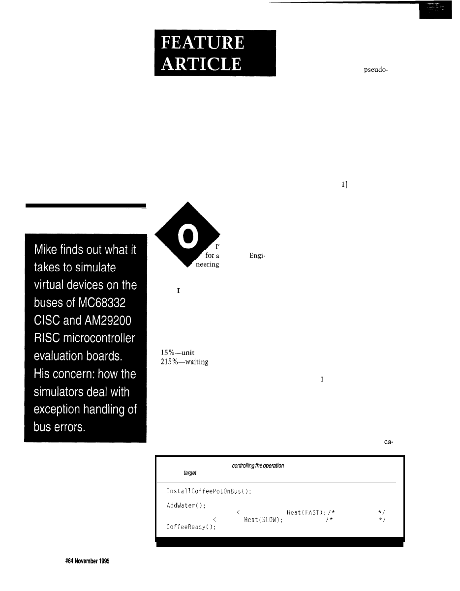
Michael Smith
Developing a Virtual
Hardware Device
ver the last year,
I’ve taken courses
a Software
Management
certificate, which has refreshed my
knowledge of how the “real” world
works. now know that an industrial
software project’s time is divvied out
like this:
Let’s consider the differing re-
quirements for simulating virtual
devices placed on the buses of the
Motorola MC68332 CISC and the
Advanced Micro Devices Am29200
RISC microcontroller evaluation
boards. The simulations use the excep-
tion handling and I/O capabilities of
the evaluation boards’ operating sys-
tems to implement the virtual device.
We’ll look into the different ways
interrupts are handled with RISC and
CISC processor architectures.
l
30%-requirements analysis
l
25 %-coding
l
15 %-review process
l
testing
l
for hardware
To minimize the simulation’s
programming requirements, I’ll use a
virtual coffee pot. The device’s code is
placed on the Circuit Cellar BBS.
SIMULATION REQUIREMENTS
The cost of waiting has created a
Listing shows how a real coffee
need for device simulators. A virtual
pot, physically attached to a controller
device shares the characteristics of a
on an evaluation-board bus, might
real device but is built entirely in soft-
operate. A virtual coffee pot should
ware. You can move and read values or
run the same code using the same
cause actions with the device registers
device-register accesses.
just as if the device was attached to
From the pseudocode, it’s clear
the processor bus!
that a virtual coffee pot must be
With such software devices, you
can integrate and test before the hard-
ware arrives, making it easier to sched-
ule development time and people.
Suppose you design a
device to speed a software project’s
development. What do you need to
simulate? If you use a virtual device
with a stand-alone evaluation proces-
sor board, what resources on that
board support your simulation?
As a Motorola course book points
out, “The quality of a simulation is
not measured by how accurately it
simulates a device, but instead by how
effectively it trains the programmer to
do the right thing when dealing with
an actual device.“[ Keeping this in
mind, here’s one way to simulate the
operation of virtual devices.
Listing l--The pseudocode for
of a real coffee-pof device is the same no matter
what the
processor.
controlregister = RESET;
while (temperature HOT-ENOUGH)
Heat water
while (timer READY)
Perk coffee
36
Issue
Circuit Cellar
INK@
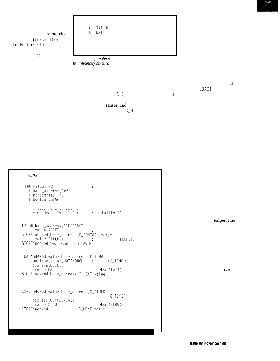
pable of handling a number of
operations. It must:
l
recognize that the
viceexists
. set the rate for heating the
water. Heat
corresponds
to writing a control value to
a device register.
l
access and change the t. i me r
and temperature values
Offset Mnemonic
Description
0x00
Initialization of device
0x10
Power-levelcontrolon heater
0x20 C-TEMPERATURE
Currentwatertemperature
0x30 C-TIMER
Timewaterhasbeen heated
0x40 C-WATER
Opens and closesvalvesto
add water
Table l--The
defined for a COFFEEPOT device controller include
the
about fhe state of the device.
In simulating the actual device’s
l
handle other register accesses
that
may produce multiple simulation
operations
operation, COFFEEPOT must:
. store a value in
0 NT RO L that
resets C-HEAT control, C-TEMPER-
ATURE
C-TIMER
l
store a value in the
EAT register
that
modifies C-TEMPERATURE's rate
of change
Now let’s examine how to use an
evaluation board’s resources to imple-
ment a coffee-pot simulation that
supports these operations.
DEVICE DEFINITION
In defining a virtual device’s func-
tionality, first specify the registers that
control and manipulate it. Table
1
gives the register description for the
l
simulate heat transfer (i.e., pot cool-
ing) when a heating element is not
high enough
l
access C-TEMPERATURE and display a
status message
. measure the time since the coffee pot
coffee-pot device.
was plugged in.
Listing
virtual COFFEEPOT device can be implemented using Am29200 assembly language.
register definitions
main:
Code here to set register and memory stacks
CALL
NOP
CONST
C-CONTROL = RESET;
CONST
C-WATER =
value
CHECKBOILING:
CPGE
while
HOTENOUGH)
JMPT
CONST
JMP CHECKBOILING
NOP
(Could fill this delay slot)
BOILED:
CPGE boolean,value,READY
while
READY)
JMPT
CONST
base-address
JMP BOILING
NOP
(Could fill this delay slot)
COFFEEREADY:
Using these register defini-
tions and requirement state-
ments, let’s program the RISC
and CISC evaluation boards to
operate on the coffee-pot de-
vice. Listings 2 and 3 show the
necessary, but inefficient, as-
sembly language code for the
Am29200 RISC and MC68332
CISC processors.
To show the equivalence
of the base device operation for these
very different processors, Listing
defines Am29200
ndexed and
R E i n d exe d macros equivalent to
the MC68332 indexed instructions.
The similarity of the code at this
level contrasts with the different cod-
ing practices needed for the underlying
simulation. It becomes apparent later
why the full range of MC68332 CISC
MO V E instructions can’t be used to
access the virtual device. The same
code should be required to operate
C 0 F F E E POT, whether the device is real
or virtual.
But, how can we change, check, or
read the heating, timing, or tempera-
ture registers on a virtual device when
none of them exist!
CONNECT THE VIRTUAL DEVICE
It’s easy to simulate the basic
operation of reading and writing the
virtual device registers-simply dedi-
cate some RAM space for those regis-
ters. However, the simulation is rather
unrealistic because the
and timer-register contents never
change. And, writing to one device
register doesn’t affect other registers.
For useful values, a background
process must perform operations such
as changing the pseudotimer and tem-
perature values. Adding a true multi-
tasking environment to produce a
real-time simulation is not a
minute job, especially on top of the
board’s existing operating system.
Since we don’t need this much realism
for a coffee pot, we can use a standard
programmer’s trick: we can fake it.
Suppose a series of pseudodevices
is sitting at locations not occupied by
anything valid on the evaluation
board’s bus. For the SA29200 board,
the addresses can be in the DRAM
memory range of 0x50000000 to
Circuit Cellar INK@
3 7
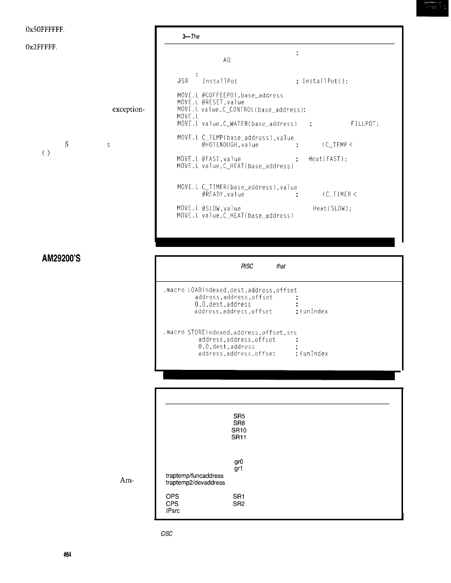
For the MC68332 board,
they can be in the range 0x20000 to
Accessing these memory
locations immediately introduces a
bus error, causes an exception, and
crashes the program. The processor is
taking notice of the virtual devices.
If the vector for the bus error’s
exception-handling routine is adjusted,
it can be steered to our own
handling routine. In this handler, I can
implement any operation I want when
the virtual device registers are ac-
cessed. Listing gives the I n t a 1 1
Pot routines for the Am29200 and
MC68322 microcontrollers.
I’m sticking to virtual device op-
erations only during device-register
accesses. Combining the bus error
exception-handler form of register
modification with one performed at
specific intervals under the on-chip
timer’s control offers better event
simulation when accurate timing is
important.
THE
VIRTUAL DEVICE
Let’s assume a virtual coffee pot is
attached to the bus of the Am29200
evaluation board. When it reads or
writes to one of the virtual device
registers, a bus-error trap occurs. This
catapults us to the exception-handling
routine PSEUDODEVICE.
As in any processor, the bus-error
trap causes a context switch on the
Am29200. Thus, the state of all previ-
ous activity must be preserved until
after the exception has been handled.
No user or system resources can be
modified during the exception until
after they’ve been saved. The excep-
tion handling is then transparent to
the processes that use it.
These requirements produce dif-
ferent results on the register-rich,
highly pipelined RISC Am29200 than
they do on the CISC MC68332. I’ll
explore some of the basic differences
between exception handling on these
processor architectures.
Table 2 shows the various
29200 registers dedicated for exception
handling with their mnemonics. These
dedicated registers can speed excep-
tion-handling on a RISC processor,
eliminating much of the slower mem-
ory-stack storage needed to handle
Listing
virtual COFFEEPOT device can also be implemented in MC68332 assembly code
value
equ DO
base-address equ
register definitions
main:
Code here to set stack
C-CONTROL = RESET;
FILLPOT,value
C-WATER =
CHECKBOILING:
CMPI
BGE
BOILED
JMP
CHECKBOILING
BOILED:
CMPI
while
READY)
BEQ
COFFEEREADY
JMP
BOILED
while
HOTENOUGH)
COFFEEREADY:
Listing
4-Macros for the Am29200
processor
provide equivalents for the MC68332 C/SC
processor indexed-memory operations ease parallel code development.
ADD
(Index address)
LOAD
(Get Value)
SUB
address)
.endm
ADD
(Index address)
STORE
(Store Value)
SUB
address)
.endm
Mnemonic
CHA
Register
S R 4
CHD
CHC
PC0
PC1
PC2
SR12
ALU
SR132
Register Function
Frozen memory CHannel Address register
Frozen memory CHannel Data register
Frozen memory CHannel Control register
Frozen old PC value
Frozen old PC value
Frozen old PC value
Frozen ALU status register
Marker to indicate using indirect register pointers
Current Register Stack Pointer
Dedicated General Register
Dedicated General Register
Current Memory Stack Pointer
Current Old Processor Status
Current Processor Status
Current Indirect Pointer A register
useindirect
rsp
msp
gr121
gr122
gr127
SR129
Table 2-Use
of registers in exception handling on the Am29200 eliminate slower memory-stack storage necessary
on
processors.
38
Issue
November 1995
Circuit Cellar INK@
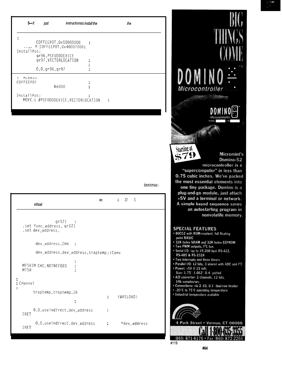
Listing
fakes
a handful of
bus error handlers on Am29200 and
MC68332 microcontrollers.
Am29200 microcontroller bus error handler set-up
.equ
virtual device
equ
real RAM locations
LADDR
LADDR
Bus error vector
JMPI rtnaddress
(In delay slot, as we return)
STORE
(store addr in vector location)
MC68332 microcontroller bus error handler setup
equ $20000
virtual device
P-COFFEEPOT equ
real RAM locations
(Store addr in vector location)
Bus error vector
RTS
exceptions on CISC processors. When
the exception handler is entered, the
disable-interrupt bits in the current
processor status register (CPS) are
activated and the original status is
saved in the old processor status regis-
ter (OPS). Of the 192 general and local
registers on Am29200, registers gr121
and gr122 are typically dedicated as
temporary registers during exceptions.
They needn’t be saved unless multiple
levels of exceptions are handled.
A unique feature of exception
handling on the Am29200 is that the
processor is said to be “frozen” when
it enters the exception handler. This
state is signified by the Freeze bit in
the CPS register.
To get the most from a pipelined
processor, data and memory accesses
must be handled in parallel with in-
struction execution. For best perfor-
mance, data access may end up far
removed from its initiating
Listing 6-A bus error exception handling routine can be used implement OA and TORE operations
on Am29200
device registers.
.equ NOTNEEDED, 0x2
.set traptemp,
register definitions
gr122
PSEUDODEVICE:
MFSR
(Grab address fault info)
LADDR traptemp, (P-COFFEEPOT COFFEEPOT)
ADD
to physical space:
MFSR
traptemp,CHC
(Grab control info)
(Tell processor 'JUNK I/O OPERATION')
IPsrc,traptemp
(Remember register indirection)
The following operation shifts the LOAD/STORE bit from the
Control register into a BOOLEAN TRUE/FALSE
position to control a conditional jump
SLL
JMPF traptemp,HANDLESTORE
if
NOP
(delay slot)
HANDLELOAD:
LOAD
reg = *dev_address;
HANDLESTORE:
STORE
else
= reg;
Circuit Cellar INK@
Issue
November 1995
3 9
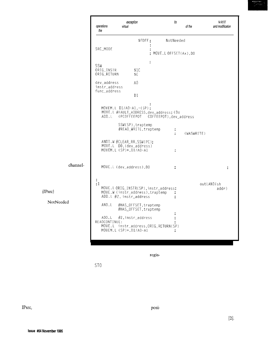
tion. In fact, the instruction code may
be flushed from the processor before
data access is complete. This flushing
action can cause complications if an
interrupt occurs before memory access
finishes.
On the AMD 29k processors,
memory access is controlled by a dedi-
cated data channel and several chan-
nel-support registers. If an exception
occurs, the processor updates the chan-
nel registers to reflect the status of the
current memory access.
To avoid overwriting the registers,
further interrupts are blocked, and the
Freeze bit is set to reflect the use of
the channel registers. A quick snap-
shot of the instruction memory’s ac-
cess pipeline is taken and stored in the
dedicated registers PCO-PC2. These
buffer registers act as program coun-
ters to restart the Am29200 instruc-
tion pipeline after the exception.
The three memory-channel regis-
ters are used to indicate the state of
memory activity before the exception.
Information about the type of opera-
tion and register in use when the bus
error occurred is stored in the
control register (CHC). The location of
the error is stored in the channel-ad-
dress register (
CHA
). Information in
the CHC register and the indirect
register pointer
can be used to
implement pseudodevice operations.
This register has a
flag
which can abort the memory operation
causing the bus-error exception trap.
The architecture of the AMD 29k
processors means that all 192 local and
general registers have direct access to
the ALU and memory. However, the
special registers (SR) must be moved
into a local or general register via a fast
register-to-register operation before
they can be manipulated.
Listing 6 shows exception han-
dling of LOAD and STORE values on the
pseudodevice registers. First, the vir-
tual COFFEEPOT address in CHA is
translated into physical memory space
(PCOFFEEPOT). Next, CHC is modified
to abort the old memory access. Infor-
mation about the register used during
the memory operation is then saved
into
which controls the indirect
Listing 7-A bus error
handling routine can be used implement limited READ and
on MC68332
device registers. Some decoding
faulting instruction
of stack frame is necessary.
CLEAR-RR
equ
READ-WRITE
equ $40
equ $38
HAS-OFFSET
equ $28
FAULT-ADDRESS equ $14
equ $22
equ
equ
equ
equ Al
equ Al
traptemp
equ
PSEUDODEVICE:
Clear
flag
Read/write* flag
Mask for determining READ mode
type instruction
Address on stack after register save
Special Status Word
register definitions
only move INDIRECT using DO register!
(Create temp. registers)
memory translation)
MOVE
AND
(Was it a READ or a WRITE?)
BNE
HANDLEREAD
if
HANDLEWRITE:
(Tell processor, we'll do writes)
*dev_address = DO;
(Recover registers)
RTE
HANDLEREAD:
else DO = *dev_address
; The rest of the READ gets trickier as we must decode the faulting
instruction and adjust the RETURN PC on stack accordingly
word if we SEE it's indirect, 2 words if with
offset
(Get instruction
(then orig instruction)
(Get over instruction word)
CMP.L
BNE
READCONTINUE
(If OFFSET, inc RETURN PC)
(over the constant)
(Restore fixed RETURN PC)
(Recover registers)
RTE
Finally, the channel-control
ter is examined to see whether a LOAD
or
RE operation is needed. This
section of code makes use of another
unique feature of the 29k architecture.
COMPARE instructions set a boolean
flag that can be stored in any register.
This construct speeds the operation of
the pipeline. The LOAD or STORE indi-
cator bit in CHC is shifted by an S L L
instruction into this boolean flag
After the necessary operation to
the pseudodevice registers, an I RET
instruction initiates recovery. It “un-
freezes” the processor, refills the in-
struction pipeline, and enables the
interrupts again, thereby servicing the
pseudodevice. No memory operations
are required to recover registers or
other status information during the
exception return.
For more detailed information on
the 29k exceptions, read the Am29200
user manual or Dan Mann’s book
use of any register as a source register
tion to control the conditional jump
for a later instruction.
that follows.
40
Circuit Cellar
INK@
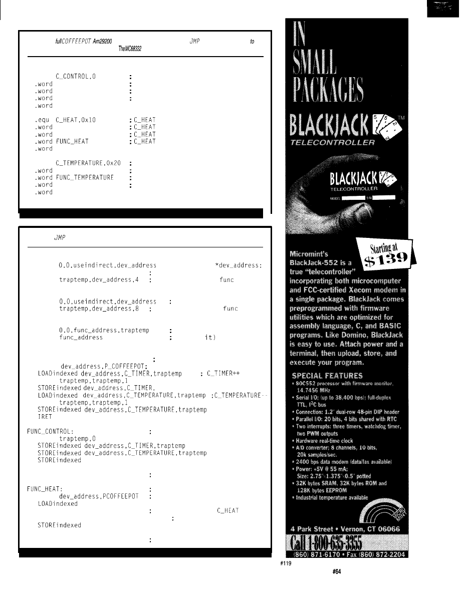
Listing 6-The
virtual device description includes
fable
information
add functionality into the device’s operation.
virtual
device description is similar.
COFFEEPOT:
.equ
0
STANDARD
FUNC_CONTROL
0
C-CONTROL offset
C-CONTROL register value
C-CONTROL LOAD function
C-CONTROL STORE function
0
STANDARD
0
offset
register value
LOAD function
STORE function
.equ
C-TEMPERATURE offset
0
C-TEMPERATURE register value
C-TEMPERATURE LOAD function
STANDARD
C-TEMPERATURE STORE function
0
etc.
Listing 9-A
table provides functionality on the Am29200 pseudodevice.
HANDLELOAD:
LOAD
register =
JMP
JUMPTABLEACTION
(In belay slot)
ADD
(prepare for LOAD
access)
HANDLESTORE:
STORE
*dev_address = register:
ADD
(Prepare for STORE
access)
JUMPTABLEACTION:
LOAD
(Grab JUMP address)
JMPI
(and do
NOP
STANDARD:
When any register accessed
LADDR
(Get base address)
ADD
traptemp
SUB
When C-CONTROL reg accessed
CONST
dev_address,C_HEATER,traptemp
JMP
STANDARD
NOP
(Could be filled)
when C-HEATER register accessed
LADDR
(Get base address)
dev_address,C_TEMPERATURE,traptemp
C-TEMPERATURE +=
ADD
traptemp,useindirect,traptemp
NOTE ORDER
dev_address,C_TEMPERATURE,traptemp
JMP
STANDARD
NOP
(Could be filled)
Circuit Cellar
INK@
Issue
November 1995
4 1
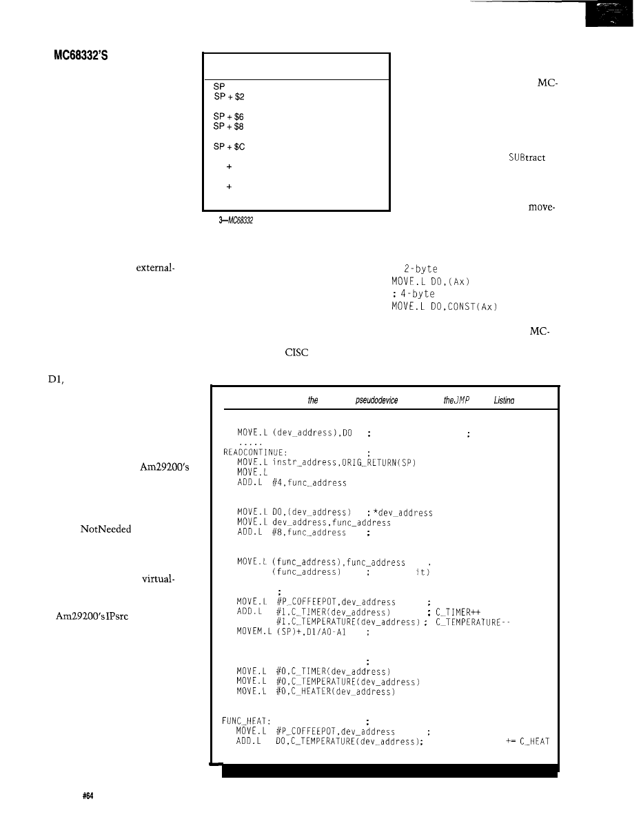
THE
VIRTUAL
DEVICE
Differences between the archi-
tecture of the MC68332 CISC and
Am29200 RISC microcontrollers
show up immediately when excep-
tion handling is examined more
closely.
Listing 7 shows how reading
and writing of the MC68332 virtual
device registers are controlled. Be-
fore the bus error’s exception-han-
dling routine is entered, any register
altered by the fault instruction is
automatically restored to its original
value. A lot of status information
Stack
Address
Contents
copy of Status Register
return PC high word
return PC low word
vector info
faulting address high word
faulting address low word
DBUF high word
DBUF low word
SP $10
faulting instruction PC high word
faulting instruction PC low word
SP $14
internal transfer count register
SP + $16
Special Status Word
Table
stack
information is shown for a bus error
exception.
[see Table 3) must also be stored to and
use the DO register, which is not as
later recovered from the
memory stack. This feature contrasts
with the faster register-to-register
operations in the Am29200 exception
handler.
In the MC68332 exception-han-
dling routine, you first free up some
temporary registers. This step requires
further memory accesses since regis-
ters
AO, and Al are saved to the
external stack. As we’ll see later, regis-
ter DO plays a critical role in the de-
vice simulator and can’t be used as a
temporary register.
The Special Status Word (SSW)
stored on the stack plays the same role
as some of the bits in the
CHC. The SSW contains information
of the size and type of data transfer,
key cycles, and function code. The RR
bit in the SSW is the MC68332 write
operation’s
bit. The RW
bit describes whether a read-from or
write-to memory operation accessed
the virtual device.
The CISC processor’s
device operations present new prob-
lems. For a start, there is no equivalent
to the
register that
enabled us to determine which data
register or addressing mode is being
used.
To overcome this problem, we
need to use the information on the
stack to find the instruction accessing
the device registers. The effective
address then has to be decoded. Such a
complete simulation is, for present
purposes, probably not necessary.
It is far simpler to permit only
virtual-device memory operations to
limiting as it might seem. It is com-
mon programming practice to use DO
as a temporary register in code access-
ing external devices. However, it is
important to ensure that this practice
is followed in compiler-generated code.
A bigger problem is determining
which MC68332
instruction
accesses the device. On the Am29200
RISC processor, you LOAD or STORE
any register using an address stored
in any another register. On the
68332, however, you can access
memory with many instructions. A
lot of code would be needed to simu-
late all possible instructions and
addressing modes.
Support for ADD and
instructions is not a normal feature
with device registers, so the simula-
tion is not limited significantly if
we require that only indirect
write instructions are used on the
virtual-device registers. Thus, opera-
tions like these are permitted:
;
instruction
instruction
These operations use one of the
68332 address registers (Ax) and a pos-
sible fixed offset (CONST) from the
device’s base address.
Listing
IO-Functionality for MC68332
is provided via
table of
8
HANDLEREAD:
DO = *dev_address
(Restore the fixed RETURN PC)
dev_address,func_address
; (Set up function pointer)
JMP
JUMPTABLEACTION
HANDLEWRITE:
= DO;
(Set up function pointer)
JUMPTABLEACTION:
(Grab JUMP address)
JMP
(and do
STANDARD:
(When ever a device register is manipulated)
(Set base address)
SUB.L
(Recover temp. registers)
RTE
FUNC_CONTROL:
when C-CONTROL register accessed
JMP
STANDARD
when C-HEATER register accessed
(Set base address)
C-TEMPERATURE
JMP
STANDARD
42
Issue
November 1995
Circuit Cellar INK@
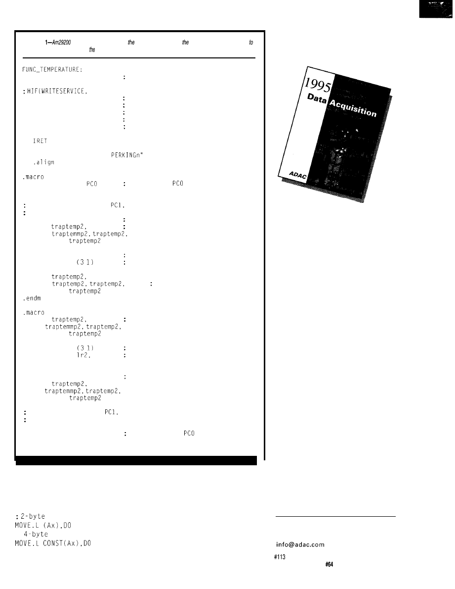
Listing 1
registers must
be saved, processor unfrozen, and interrupts released prior
operating system calls in middle of a bus error interrupt handler.
SAVEREGISTERSANDUNFREEZE macro
STDOUT, MESSAGEPT, MESSAGELENGTH
CONST
gr121, 20
WRITESERVICE
CONST
lr2, 1
STDOUT
LADDR lr3, MESSAGE
MESSAGEPT
CONST lr4, 15
MESSAGELENGTH
ASNE 0x45, grl, grl
HIFO;
FREEZEANDRECOVERREGISTERS; macro
MESSAGE: .ascii "COFFEE
SAVEREGISTERSANDUNFREEZE
MFSR traptemp,
save FROZEN
SUB msp, msp, 4
STORE 0, 0, traptemp, msp
Save also SR registers
ALU, CHA, CHD, CHC. OPS
and standard register gr96
CONST traptemp, 0x400
FREEZE BIT
MFSR
CPS
being cleared
ANDN
traptemp
MTSR CPS,
SUB msp, msp, 12
Burst save of lr2, lr3, lr4
MTSR CNT,
registers
STOREM 0, 0, lr2, msp
MFSR
CPS
ANDN
0x3
Reenable interrupts
MTSR CPS.
FREEZEANDRECOVERREGISTERS
MFSR
CPS
Disable interrupts
OR
0x3
MTSR CPS,
MTSR CNT,
Burst recovery of lr2, lr3, lr4
LOADM 0, 0,
msp
registers
ADD msp, msp, 12
CONST traptemp, 0x400
REFREEZE processor
MFSR
CPS
OR
traptemp
MTSR CPS,
Recover SR registers
ALU, CHA, CHD, CHC, OPS and gr96
registers in the reverse order were pushed onto the stack
LOAD 0, 0, traptemp, msp
MFSR PCO, traptemp
recover FROZEN
ADD msp, msp, 4
.endm
Even with these restrictions, sim-
ulating the following READ instruc-
tions gets more complicated:
Listing 7 indicates the extent of this
complexity.
After a bus error produced by a
write operation, the exception-stack
frame has a return-PC value that corre-
sponds to the instruction after the
faulting W R I T E instruction. In con-
trast, the same return-PC value for the
instruction
;
instruction
FREE
Data Acquisition
Catalog
PC and VME data
acquisition catalog
from the inventors of
plug-in data acquisition.
Featuring new low-cost
A/D boards optimized
for Windows,
DSP Data Acquisition,
and the latest
Windows software.
Plus, informative
technical tips and
application notes.
Call for your free copy
l-800-648-6589
ADAC
American Data Acquisition Corporation
70 Tower Office Park, Woburn, MA 01801
phone 617-935-3200 fax 617-938-6553
Circuit Cellar
INK@
issue
November 1995
43
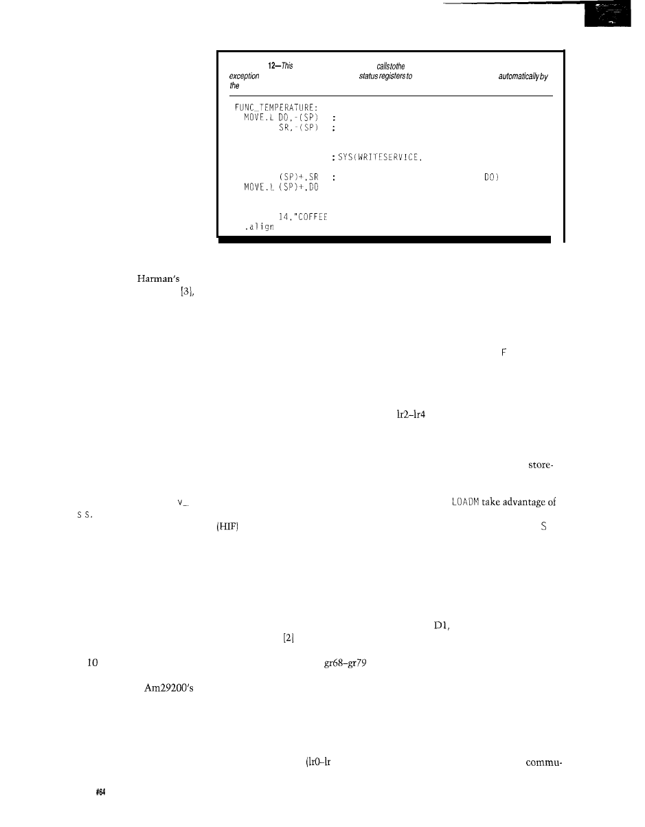
read bus-error fault points to the in-
struction that caused the fault.
This address must be modified by
2 or 4 bytes, depending on whether the
indirect MOVE has an offset. The fault-
ing instruction must be fetched from
memory and its effective addressing
mode must be determined.
At the end of the MC68332 excep-
tion handler, the original values of the
temporary registers must be recovered
from memory. Issuing RT E recovers
other status information from the
stack. The processor restarts program
execution after the memory access
that produced the bus error. Again, the
pseudodevice has been serviced.
I gained information on bus-error
handling from Thomas
book
on the MC68332 microcontroller
the CPU32 CPU reference manual, and
trial-and-error techniques.
GETTING ACTION
Up to this point, we have provided
the virtual device with registers that
can be written to or read from. How-
ever, it still has no functionality.
One way to introduce functional-
ity is to place J M P table information
directly into the device description.
Listing 8 shows the format for part of
this new device description and Listing
9 shows how to introduce functional-
ity into the Am29200 simulation.
Information about the virtual
device register is contained in de
add r e If this register is increment-
ed by 4 or 8, it points to a location
containing the address of the function
to perform following a read or write
operation on a device register. An
indirect J M P with the appropriate start
address switches the exception handler
to the required function.
Each function is completed by
jumping to STANDARD, which modifies
TIMER and TEMPERATURE registersto
better model device properties.
Listing enables the functional-
ity of the MC68332 virtual coffee pot.
Note the similarity with
code. Register DO doesn’t need saving
since its functions don’t change. Func-
tionality on other devices may require
DO and/or additional data registers
that need saving to the stack so access
remains transparent.
FOR FLAVORED COFFEE
A simulation should also display
status or debug messages. These fea-
tures involve using the evaluation
board’s operating system to perform
system calls to communicate with the
PC providing a keyboard and screen.
This communication typically occurs
over a serial communication link be-
tween the PC and evaluation board.
To use this link, registers used
during the call must be saved. Also,
the interrupts for the boards must be
reactivated so serial communications
can be reestablished. This reconnec-
tion is done by the operating system
on the MC68332 evaluation board, but
by the user on the SA29200 board.
Listing 11 demonstrates how to
make use of calls to the Am29200
evaluation board’s high-level interface
during a bus-error exception
handler. A status message about the
coffee-pot operation displays each time
the C-TEMPERATURE register is read.
Two steps reactivate the inter-
rupts and unfreeze the processor dur-
ing the current exception handling
routine. First, save the frozen registers
and any other necessary registers.
Dan Mann describes a fast
context-switching approach that sets
aside Am29200 registers
for
a register cache that stores the frozen
special registers. To simplify this sim-
ulation, all the registers are stored to
external memory using the Memory
Stack Pointer (MSP). MSP must be
distinguished from the Register Stack
Pointer (RSP), used to control the RISC
register window cache
127).
Listing
is a technique for making
MC68332 board’s operating system during an
handler. The saving of important
external memory is handled
processor.
(Used as temp register during SYS call?)
MOVE
(Not necessary for this example?)
(Monitor did I/O without needing changes to interrupt levels)
PE
A
MESSAGEPT
TRAP 15
MESSAGEPT)
DC.6
WRITESERVICE
MOVE
(Recover status register and
JMP
STANDARD
MESSAGEPT:
DC.6
PERKING"
4
After saving the Am29200 special
registers, the processor must be unfro-
zen and the interrupts reenabled. Be-
cause of the way the pipeline buffer
(PCO-PC 1) is reestablished, two in-
structions must occur between the
processor unfreezing and enabling the
interrupts. After the H I call, the in-
verse operations must occur before an
I RET call completes the bus-error
exception-service routine.
Since the
H I
F call uses registers
and gr96, they must also be
saved on the memory stack. The chan-
nel registers become active again once
the processor is unfrozen. Registers
can then be fast-stored using a
multiple instruction and recovered
with a load-multiple instruction.
STOREM and
the faster burst-access memory mode.
Listing 12 demonstrates a SY call
to the MC68332 board’s monitor to
display a status message. The code
appears simple because most opera-
tions occur internally to the SY S call,
not externally as with the SA29200
board’s
H I F call.
It is not clear whether local regis-
ters DO,
AO, and Al are modified
during the SYS call, so the safest ap-
proach is to save them onto the stack.
Only DO must actually be saved, since
the others already have been placed on
the stack. The other status informa-
tion needed to restart the user program
was stored to the stack when the origi-
nal bus-error trap occurred.
It is not necessary to modify the
status register in order to reenable the
interrupts and reestablish the
44
Issue November 1995
Circuit
Cellar INK@
nications link. This happened auto-
matically during the SY S call.
WHERE TO NEXT?
For more comprehensive memory
operations on the Am29200 and
68332 pseudodevices, a small amount
of additional code could offer memory
operations with 16-, or 32-bit ac-
cess. However, this doesn’t solve the
problem that MC68332 pseudodevice
access is limited to one data register
(DO) and indirect MOVE
S
.
Advanced Micro Devices has both
an architectural and an instruction set
simulator for the Am29200. Software
Development Systems provides an
MC68332 simulator in their C/C++
68k starter kit. A really caffeine-free
next step would be to hang COFFEEPOT
on pseudoprocessors!
I hope to examine other tech-
niques to get fuller functionality out of
virtual devices. I’d like time-accurate
simulations and calls accessing replay
files on the PC driving the evaluation
board. The pseudodevice could then be
tested with real data.
q
Special thanks to the University of
Calgary for a sabbatical to follow up
on research and teaching ideas.
Mike Smith is a professor in the Elec-
trical and Computer Engineering De-
partment at the University of Calgary,
Canada. He teaches courses on
Ctt,
microprocessor interfacing, and com-
parative processor architecture and
does research into digital-signal-pro-
cessing applications for
resonance image reconstructions.
Mike may be reached at
Motorola, “Gathering Re-
quirements,” Motorola Uni-
versity Course Notes, 1993.
Dan Mann, Programming the
29k RISC Family,
Data Book
1995.
Thomas
The Motor-
ola MC68332 Microcontrol-
ler-product design, assembly
language programming and
interfacing,
Prentice Hall,
1991.
Advanced Micro Devices
901 Thompson
Sunnyvale, CA 94088
(408) 732-2400
Hotline: (800)
Motorola
2100 East Elliot
Tempe, AZ 85284
(602) 244-6900
Fax: (602) 952-4067
Software Development Systems
815 Commerce Dr., Ste. 250
Oak Brook, IL 60521
(708) 368-0400
Fax: (708) 990-4641
407
Very
Useful
408 Moderately Useful
409 Not Useful
DOS IN ROM!
programs Also
in
protection viruses.
Easy to half-size
5 7 5
1 44m 5150
5 1 9 5
$95 EPROM
PROGRAMMER
S u p e r F a s t P r o g r a m m i n g
to use than others
D o e s 2 7 6 4 1 2 7 0 8 0
M e g ]
STARTS AS LOW AS
Professional schematic
PCB design Software for
Windows 3.1
l
Automatic wire routing
dot placement.
l
Exports diagrams to
other
l
Full
control of drawing
appearance.
R4 SYSTEMS
1100 GORHAM ST.
N E W M A R K E T O N T A R I O
C A N A D A
all the
of
of CAD
. Advanced routing
l
Libraries, including SMT
l
Includes Gerber Viewing
l
Fast Easy to use.
F R E E D E M O
W R I T E O R C A L
898.0665
FAX
Circuit Cellar
INK@
Issue
November 1995
4 5
Ed Lansinger
Developing an Engine
Control System
Part 3: Completing the System
0
his month,
wrap up my series
on the electronic
injection system I devel-
oped for Rensselaer’s race car. I created
the Motorola
system
while a member of the Formula SAE
team. In the past two articles
62
and
I covered the fuel- and
delivery subsystems.
Three simple but important cir-
cuits round out the hardware: crank-
shaft-position detection, automatic
shutdown, and power supply. In
ware,the Distributor and
C 1 o c k objects catch the interrupts that
initiate all software activity, and the
MAP object reads the air-pressure sen-
sor. I finish by describing the basic
process of testing and tuning the com-
plete system.
HARDWARE
To synchronize control events
with crankshaft position, the engine
(from a Yamaha
motorcycle)
has teeth cut in its metal flywheel. As
the engine turns, the teeth pass close
to a variable-reluctance pickup called
the
crankshaft-position sensor
(CPS).
Figure 1 shows this arrangement.
The sensor produces a current
pulse as the teeth pass. The pulse’s
direction is determined by whether the
edge of the tooth is leading or trailing.
The pulse is detected by the crankshaft
position-sensing circuit in the Engine
Control Module (ECM). Figure 2 shows
the crankshaft position-sensing circuit.
The circuit’s core is the full-wave
bridge rectifier formed by Dl-D4 that
is open at one end. A current pulse
loops up through D2, into the base of
Q2 (turning it on), to ground, through
D3, then back to the sensor. A current
pulse traveling in the opposite direc-
tion makes a similar loop but through
and D4.
and Q2 pull low two separate
lines that are tied high to V. These
lines are interrupt lines to the process-
or. In this way, the processor is inter-
rupted on both leading and trailing
edges and can tell them apart. The
ability to differentiate between the
two is important for detecting the
unique Top-Dead Center (TDC) tooth
[explained in “Software”).
and
must be high-gain
transistors because the crankshaft
position sensor doesn’t push a lot of
current at low
work
fine and are ubiquitous, although their
power-dissipation rating is unnecessar-
ily high for this circuit.
More subtle is the requirement
that Dl-D4 be germanium diodes like
the
At cranking speeds, the
CPS produces output voltages barely
more than a couple of volts. The for-
ward voltage drop of two silicon diodes
(0.7 V each) and the transistor’s
to-emitter voltage drop (about 1.4 V)
blocks this signal.
By using germanium diodes (for-
ward voltage drop of only 0.3 V), the
overall drop reduces enough to ensure
reliable starting. This problem goes
away at higher engine speeds. In fact,
the CPS develops open-circuit voltages
of several hundred volts near the red-
line!
The Automatic Shutdown (ASD)
watchdog circuit controls the power
supply to the ignition coils, fuel pump,
and injectors. If the software hangs or
the car stalls, the ASD circuit (see
Figure 3) shuts off power to these de-
vices within 0.5 s.
This shutdown protects driver,
engine, and electronics if the ECM
fails. If the system conks out, you
46
November 1995
Circuit Cellar INK@
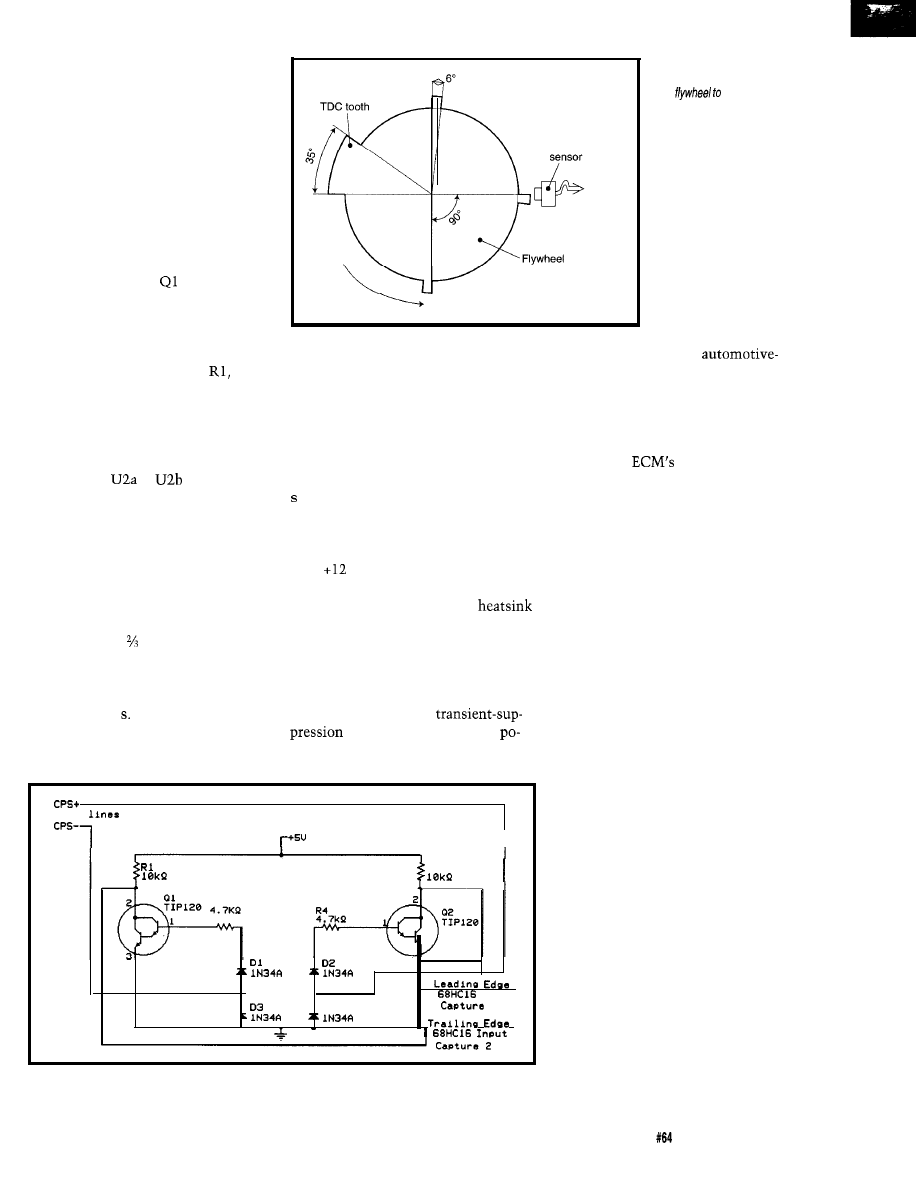
cannot have the injectors remaining
on, filling the engine with fuel while
the coils get toasty and the drive cir-
cuitry overheats. The ASD circuit
turns on the relays supplying power
directly. It is kept active by a line from
the CPU that the software must toggle
rapidly.
Rapid toggling of the line coming
from the 68HC 16 keeps voltage low on
Cl
and C2 to prevent the relay from
being shut off. When the input is a
logic high, transistor
discharges
capacitor Cl and transistor Q2 is off,
which allows C2 to charge. If we’re
lucky, the CPU changes the state of
the input line before the voltage on C2
gets above a reference set by
R2,
and R3.
When the input changes from high
to low, C2 is discharged by Q2, and Cl
begins to charge. However, if either
capacitor gets sufficiently charged,
comparators
or
detect it and
turn off the relay that gates power to
the coils, injectors, and fuel pump.
case, the line must be toggled at least
once every 0.5
This time must be slower than the
rate that crankshaft position pulses
The software toggles the line
when it receives a pulse from the CPS,
so the ignition and fuel subsystems
turn off in the event of a stall. The
values of Cl, C2, R8, and R9 set the
minimum toggle rate. Since the volt-
age reference is the supply to the
capacitors, the reference voltage is
reached in about
R x C
seconds. In this
Crankshaft position
to ECM
generated when the
starter motor turns
off.
Current for the
(end of crankshaft)
starter motor comes
directly from the
Direction of rotation
occur at cranking speeds. Our engine
typically cranks at around 200 RPM.
There are four teeth on the crankshaft,
so the time between pulses is generally
no longer than 75 ms. When the en-
gine is cranking very slowly during
cold starts or when push-starting the
car, the extra time allowed by that 0.5
toggle helps, and it’s still a short
enough time for protection.
battery. For simplic-
ity, it is controlled by
a dashboard switch,
rather than the ECM.
The switch turns on an
starter relay, sending current to the
starter motor.
The power supply (see Figure 4) is
straightforward. The car battery sup-
plies
VDC, which is filtered and
passed to 7805 and 7808 voltage regu-
lators. The 7805 needs a large
because the total current drawn by the
ECM is near capacity. The 7808 needs
no heatsink.
protection by conducting and blowing
the fuse. Diode D2 is a
diode which clamps any
tentially harmful voltage spikes
Diode D 1 provides reverse-voltage
I n p u t
f r o m C r a n k P o s i t i o n S e n s o r
I
R2
D4
3
I n p u t
1
Figure P-Germanium
diodes he/p this circuit detect small current pulses from the crank position sensor at low
speeds.
Figure 1-A
variable-reluct-
ance sensor defects teeth on
the
determine
engine position.
Starting the engine draws about
100 A from the battery, which is
enough to lower the battery output
voltage. The
performance de-
grades as battery voltage drops mainly
because the ignition coils don’t charge
sufficiently and the engine doesn’t
crank quickly. At 10 V, the engine
runs poorly, and at 9 V, it won’t run at
all, so the battery must be well
charged before starting. A booster
battery helps during long periods of
cranking.
Shock and vibration are the big-
gest physical dangers to the ECM. If
components are not properly mounted
and flat to the board, solder joints
fatigue and crack. For extra durability,
I used silver-based solder. I mounted
the boards rigidly to their enclosure
with short standoffs. Rubber shock
mounts attached the enclosure to the
vehicle’s frame.
I then secured all wiring leading to
the box, to ensure that the box wasn’t
supporting the weight of the wires. If
you’re really confident in your circuit,
potting it in epoxy is the way to go.
SOFTWARE
To keep injector and ignition soft-
ware synchronized with engine posi-
tion, I created the Distributor
software object. Figure 5 shows its data
members and messages.
Distributor mimics the action
of a mechanical distributor in deter-
mining which cylinder should fire
next. It also supplies information to
Circuit Cellar INK@
Issue
November 1995
47
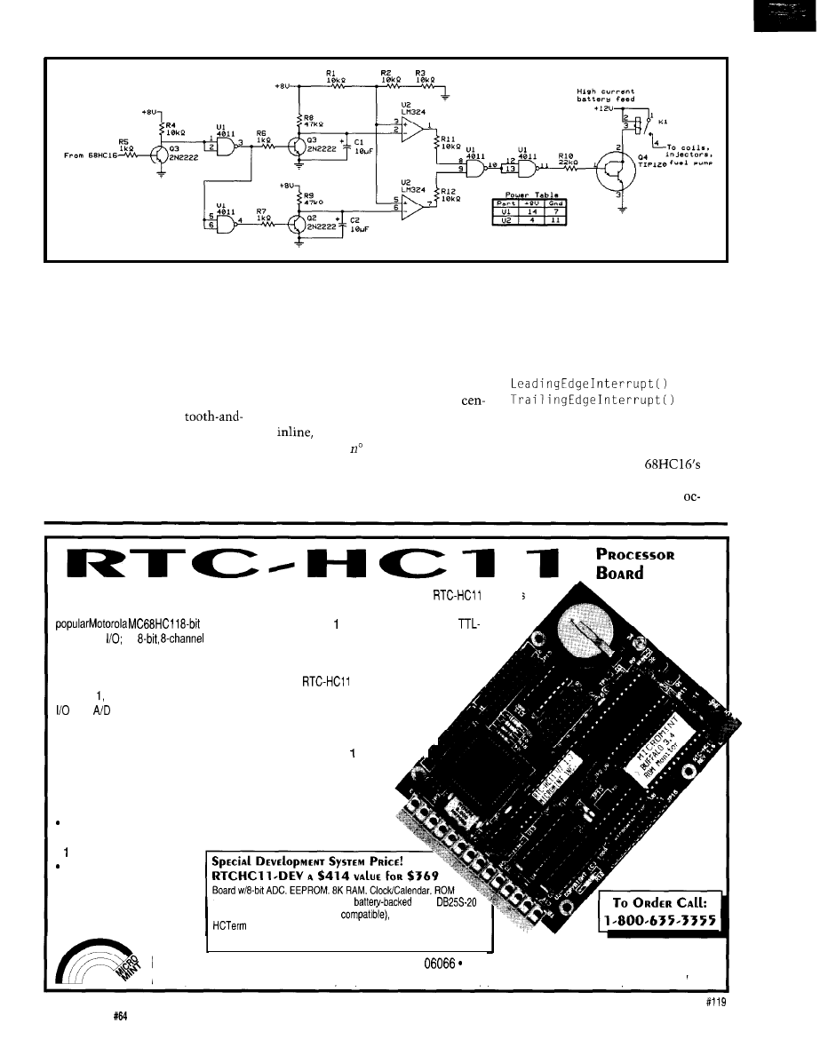
Figure 3-The automatic shutdown circuit turns the ignition and fuel off in the event of a malfunction.
other objects about engine speed and
leading edge passes the sensor before
manages the rev limiter.
the piston in cylinder 1 reaches TDC.
Determining engine position is
The piston in cylinder 4 is in
simple because of the shape of the
phase with the piston in cylinder 1.
teeth passing the CPS. Engines have
Pistons in cylinders 2 and 3 are 180”
different sense-tooth arrangements.
out of phase, so when 1 and 4 are at
Position sensing typically amounts to
TDC, 2 and 3 are at bottom-dead
detecting a variation in a
ter. This is a common arrangement for
gap pattern. This engine has three
4-cylinder engines. (When an
short teeth, each covering about 6” of
event occurs before or after TDC,
crankshaft rotation, and one long,
that is the position of the specific
covering about 35”. Leading edges are
cylinder’s piston. When I refer to a
spaced evenly at 90”. The long tooth’s
timing tooth, such as the TDC tooth,
that tooth’s position is relative to the
position of cylinder l’s piston.)
As mentioned, the teeth’s leading
and trailing edges produce unique
interrupts. These interrupts send the
and
mes-
sages to D i s t r i but o r, which allows
D i s t r i but o r
to determine engine
position easily.
I used the Motorola
Input Capture inputs to capture each
signal, record the time when it
Offering an exceptional value in a single-board embedded controller, Micromint’s
combines
all of the most-asked-for features into a compact 3.5” x 4.5” package at a reasonable price. Featuring the
microcontroller, the RTC-HCI gives you up to 21 lines of
compatible
an
analog-to-digital converter; two serial ports; a real-time clock/calendar
with battery backup; 512 bytes of nonvolatile EEPROM; and up to 64K of on-board RAM or EPROM,
32K of which can be battery backed.
Software development can be done directly on the
target system using
BASIC-1 an extremely efficient integer BASIC interpreter with dedicated keywords for
port,
converter, timer, interrupts, and EEPROM support. In addition, a flexible
configuration system allows a BASIC program to be saved in the on-board, battery-
backed static RAM, and then automatically executed on power-up. Micromint
A
also offers several hardware and software options for the RTC-HCI including
A
the full line of RTC-series expansion boards as well as an assembler, ROM
monitor, and a C language cross-compiler.
Additional features include:
Asynchronous serial port with full-duplex
RS-232 and half-duplex RS-485 drivers
l
-MHz synchronous serial port
CPU watchdog security
l
5-volt-only operation
l
RTC stacking expansion bus
monitor,
BASIC-11 in EPROM, 32K
RAM,
serial cable, utilities diskette (PC
manual set, and
software.
Other configurations starting at $199
MICROMINT, INC.
4
Park Street *Vernon, CT
(860) 871-6170
l
Fax (860) 872-2204
in Europe: 1285-658122
l
in Canada: (514) 336-9426
l
in Australia: (3) 9467-7194
l
Distributor inquiries invited!
48
Issue
November
1995
Circuit Cellar INK@
RPM
Figure
and
coils are synchronized
by the s r b r software object.
Second, I’d like to start charging a
coil at TDC at the highest
to
maximize charge time. Unfortunately,
I can’t. The spark duration for this
ECM can be as high as 1.5 ms, which
can easily extend past TDC at speeds
beyond 11,000 RPM. (TDC as mea-
sured by the sensor is actually about
13”
before mechanical TDC.) There-
fore, charging the coil at the TDC
signal interrupts the previous spark,
preventing reliable ignition. Setting
the earliest charge point at 270” before
TDC works well for this system, even
though the coils do not charge to their
fullest.
D i
s t
r i but o r limits engine speed
by cutting out cylinders above a cer-
tain RPM. If a cylinder is cut out by
the rev limiter, its Co i 1 and I n j e c
tor stop receiving
and
Open
messages. Co i 1 continues to
receive i r e
messages to ensure it
is fired safely if it has started to charge
instead of remaining on indefinitely.
After Distributor sends the
appropriate messages to Co
i
1 and
I n j e
c t o
r,
it
cleans up and returns
from the interrupt, which lets fore-
ground processing run. You can choose
Figure
objects that need to sleep”
for a while
A
k so they are reactivated
at the right
what to do in foreground (e.g., data
logging, an LCD display, traction con-
trol, etc.). The
is fast enough
that the engine control software uses
only a fraction of the available CPU
time, even at high engine speeds.
As Distributor synchronizes
Injector and Coi 1 with their me-
chanical equivalents, A 1 a
k (see
Figure 6) facilitates asynchronous
processing. It provides wake-up calls to
other objects so they can schedule
future events.
Frequently, an object needs to
perform an action at a future time. For
example, I n j e c t o r needs to turn off
its output after a certain time elapses.
Waiting in a busy loop won’t work
because other objects may need to run.
Instead, Injector
to wake it up at a future time by send-
ing it the message specified in the
wake-up request.
Al
ock tracks which mes-
sages to send to different objects. It
uses a dedicated interrupt to wake
itself up when the first message in the
queue is to be processed.
Now get C-programmable miniature controllers
with non-volatile “flash” memory. Our Dynamic
development system makes it easy-only $195. Call
our
today! Dial 916.753.0618 from your FAX
and request catalog
1724 Picasso Ave.
Davis, CA 95616
916.757.3737
916.7535141 FAX
is
a C/C++ object library containing over 1000
rectification, enhancement, image analysis, object segmen-
tation and classification, neural network applications and
2-D math/transform operations, etc. etc.
It is designed to
provide a complete set of functional tools for the development
of 32-bit protected mode DOS, WINDOWS and OS/2 applica-
tions (A SUN based version is also available);
all of which are
supported in single greyscale mode or using
full
color processing, of RGB, HSI, and YIQ true-color.
also supports the use of region-of-interest
area-selective application processing.
with
over
5000 lines
programs of sample codes
demonstrating the use of all aspects of the libraries. No royalties. Supports
most C/C++ protected mode compilers.
TARDIS Systems,
125 Los
NM 87544
(505)
fax
50
Issue
November 1995
Circuit Cellar INK@
Listing
MAP software object uses A a
k to
itself af a periodic rate
* Object MAP "Manifold Absolute Pressure" sensor
* Messages:
*
constructor
* Query: returns current manifold abs pressure quantized into O-255
called periodically via
to do filtering
equ 5244
ms at 1 tick = 1.907
* Reserve memory for MAP data members
section
equ
1
filtered MAP value
* Define MAP messages
section
>wFilteredMAP,z
filtered MAP value = 0
Ask
to send the
message a bit later
pshm
the "this" pointer
Clock wants pointer to object
tzkb
wake up
in YK:IY
tbyk
ldab
message
tbxk
to pass
ldx
;in XK:IX
ldab
"this" pointer
tbzk
;for call
(continued)
After sending the message, it finds
the next message and checks its due
time. If that time has passed, it sends
the message and checks the next one.
Otherwise, it resets its interrupt for
the time of the next message and goes
back to sleep.
A 1 a r 1 o c k also tracks global
system time. In the ECM, time is
based on the
TCNT register, a
16-bit free-running counter which
increments once every 1.907 ps. As a
16-bit counter, it wraps back to zero
every 125 ms, so it can’t time long
intervals.
A
1
a r 1 o c k responds to an inter-
rupt that occurs every time TCNT
wraps around and increments another
16-bit counter, which extends the
range to over two hours. Using
time, an object can request a wake-up
call many minutes in the future with
microsecond accuracy.
What happens after two hours!
Good question. Our race car never
runs for more than 15 min. because it
only holds one gallon of gas. But,
longer-lived applications might need to
QUALITY PARTS
l
DISCOUNT PRICES
l
HUGE SELECTION
Model 6025
back-up a” IBM PC/XT/AT, DOS 2.0 or
later. These units were designed do back-ups on a
small roll of
magnetic tape. The
are 14
4.75” 2.9” and weigh
Ibs. The heavy-gauge
metal
box
a tape
power supply
fan and other components. Also Includes IEC
power cord, data cable and 3 rolls of back-up tape
Although these are new
include instruc-
tions and software on 5.25” floppies
do not
to represent
these as
We are selling
them”AS-IS”
Nearly complete case
for SCSI
Includes 40
(5 Vdc
3 amps.
12 Vdc 2 amps)
with
fan.
power
fuse
LED socket, power
receptacle. two standard 50
SCSI Interface lacks,
power connectors,
cable
50
socket connector and
Front face plate an aftermarket piece
that doesn’t quite go
the box but serves the purpose
pretty well
Absent from the case the switch back
which
the
the
be
bypassed
a few 0.1”
SJ-I). Also not Included a standard IEC
power cord (our CAT# LCAC-60).
easy
SCSI-1
and
for the
All others
AK,
All
orders
Visit Our World Wide Web Site...
ASMO brand
12 Vdc.
gear-head motor.
motor for
Great for
and
175 RPM 12 Vdc, 1.5
amps
load). Works well from 6
24 Vdc
long dual flatted thread-
shaft (thread
lmm) Overall
6 long X 2 75” X 3.5”
leads with
connector
9 1 7 %
Interlink 7.5” 11 5” 0.03” thick
pad
two separate force
embedded
the pad. We have no factory specs or
on the Intended
for the product. It was probably
designed for
of touch
read between 1.5 Meg and 0.5 Meg when
nothing
the pad The resistance decreases to as
low as
ohms when pressure
to the pad and
appears to be dependent upon force and the amount of sur-
face area acted upon. An
for
CAT# FSR-1
Circuit Cellar
INK@
Issue November 1995
51
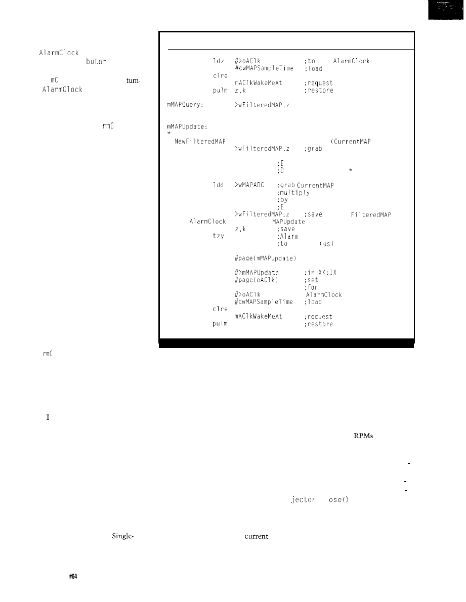
extend the timer or at least check the
system’s operation at the time limit.
also
detects
stalls.
Each time
Di stri
detects a
tooth edge, it sends a message to
A 1 a r 1
o c
k
that the engine is
ing.If
receives
no such
messages between two successive
TCNT overflows, it assumes the en-
gine has stalled. Objects register spe-
cial stall routines with
Al a
1 o c k
that are executed when this happens.
Distributor
uses this feature to set
RPM to zero and resets engine position
to
unknown.
Aside from the CPS, the only
sensor in the ECM is the Manifold
Absolute Pressure (MAP) sensor. Along
with RPM, it measures intake mani-
fold air pressure, which indicates how
much air flows into the engine. The
MAP
object represents the physical
sensor. This object reads the A/D con-
verter attached to the sensor every
10
ms and filters the reading using a
simple first-order digital filter. The
result is available to any object that
needs it.
Filtering the
MAP
value is desirable
because the air vibrates inside the
manifold due to pressure pulses from
the valves. But, too much filtering
reduces system response time, causing
poor throttle response. Listing
1
dem-
onstrates the filtering code and use of
A 1 a
1 o c k
for wake-up calls.
TESTING
The ECM was tested carefully and
rigorously. My most important rule
was to verify with an oscilloscope that
everything else was operating properly,
before
connected the fuel pump.
I
made sure that the ASD subsystem
worked, the code did not hang, the
coils fired at the right time, and the
injectors turned off when they should.
I did this to convince myself that
the engine would not be damaged, nor
gasoline spill all over the place. Just in
case, I also installed a kill switch af-
fecting all electronics, wore safety
goggles, and had another person handy
with a big fire extinguisher.
I first checked the code to make
sure it worked as expected.
stepping through every code path took
a long time but was well worth it.
Listing l-continued
the
ldd
snooze time
jsr
wake-up call
the "this" pointer
rts
ldd
rts
To filter MAP, apply the formula:
*
= (OldFilteredMAP * 0.75) +
* 0.25)
ldd
OldFilteredMAP
lsrd
tde
= OldFilteredMAP * 0.5
lsrd
= OldFilteredMAP 0.25
ade
;E = OldFilteredMAP * 0.75
from ADC
lsrd
lsrd
0.25
ade
= (Old * 0.75 + Current * 0.25)
ste
as new
* Ask
to send the
message again
pshm
the "this" pointer
Clock wants pointer to object
tzkb
wake up
in YK:IY
tbyk
ldab
;and message
tbxk
;to pass
ldx
ldab
"this" pointer
tbzk
call
ldz
;to the
ldd
snooze time
jsr
wake-up call
z,k
the "this" pointer
rts
Because the code is real-time, if it
screws up, it is virtually impossible to
backtrack to the error without an ex-
pensive logic analyzer.
I then put the engine on a dyna-
mometer to spin it and check the CPS
signal. If you don’t have a dynamom-
eter, you can do a pretty good job with
a starter motor and big battery. Make
sure neither gets too hot. Take the
spark plugs out so the engine spins
freely.
I checked that the CPS was inter-
rupting the ECM reliably and the code
was finding TDC. With all fuel and
spark hardware disconnected, I then
used an oscilloscope to verify that the
coil, injector, and ASD output signals
worked, and that the system was not
hanging. I also checked the
limiting feature of the ignition-coil
driver circuitry.
Next I checked spark timing. I
hooked up the coils and spun the en-
gine at a low RPM near idle. Using an
automotive timing light, I checked
that cylinders
1
and 4 fired as pro-
grammed in the spark-advance table.
Then, I made sure that cylinders 2 and
3 fired 180” after 1 and 4. I did this at
successively higher
to verify
that the advance changed according to
the table.
I then tested the limits of
A 1 a r m
C 1
oc
k
by having objects request extra
wake-up calls. It is vital that
A 1 a r m
C 1
o c
k
work because it sends the
I n
Cl
messages. I had
already checked all message combina-
tions: one, more than one, past-due,
early, and so on. This extra test was a
confidence check. It is especially use-
ful if you can’t spin the engine fast
enough to let messages stack up.
52
Issue November 1995
Circuit Cellar
INK@

When I felt confident that the
injectors would turn off properly, I
hooked them up, leaving the fuel
pump disconnected. I spun the engine
at various
and throttle posi-
tions, watching the spark advance
with the timing gun and the injector
pulse width with the oscilloscope. I
also cranked the engine using its start-
er motor, to make sure the
D i t
r i b
r
sent messages using the proper
low-speed firing algorithm.
Comfortable with what I saw, I
turned on the fuel. I must confess that
things did not go quite as smoothly as
this narrative suggests. It was all the
more exhilarating when the engine
finally roared to life.
Then, I began tuning for maxi-
mum power.
TUNING
For racing engines,
throttle (WOT) operation dominates
all other modes. A race car spends
roughly 70% of its time at WOT, 20%
at closed throttle, and only about 10%
at part throttle. So, I spent most of my
time tuning for Maximum Brake
Torque (MBT) at WOT and a little
time making sure the engine holds an
idle. I tuned the part-throttle range at
the track when I got the chance.
Simply put, MBT at WOT for a
given RPM is achieved with a unique
spark-advance value and a unique
injector pulse width. These values are
recorded in a look-up table. Fortu-
nately, I had access to a dynamometer
with constant-speed control which
maintained a set speed regardless of
engine output. I measured MBT spark
advance and injector pulse width for
WOT operation over engine speeds
from 4000 to 11,000 RPM in incre-
ments of 1000 RPM.
I
had guessed injector pulse width
using the ideal gas law, as described in
INK
62. To tune pulse width, I simply
set an RPM in the area I expected to
run most of the time, varied the initial
guess until I found a pulse width that
generated MBT, and recorded it. MAP
remained very close to 1 atm at WOT
regardless of RPM, so one pulse width
could be used for all
For spark advance, I started with
the manufacturer’s original timing
curve from the service manual, but
found it too conservative for MBT. At
each RPM, I increased the advance
until I found the maximum or until
the engine began to knock. If it
knocked, I recorded an advance value
2” retarded from when it knocked.
I recorded these values in the
advance table for Co
1.
As I men-
tioned in INK 63, it is important to
know what knock sounds like for a
given engine before tuning it. Heavy
knock can damage internal parts.
Both spark advance and injector
pulse width can be successfully tuned
in a vehicle. The ideal gas law and the
OEM advance curve get the engine
running well enough to power the
vehicle. From there, you can use the
seat of your pants, timing equipment,
or an in-car accelerometer. Of course,
you won’t be able to hold constant
RPM, so just look for the best accelera-
tion.
Also, don’t forget to use your eyes.
Soot coming out the exhaust is a sign
of too much fuel as are soot-covered
spark plugs. Be careful of running too
little fuel, though, which causes exces-
sively high-combustion temperatures
that can damage the engine.
If you have enough testing time,
it’s good to map advance and pulse
width for many more combinations of
MAP and RPM. With limited time,
though, you can achieve good results
by following these steps:
l
use the WOT MBT spark advance
curve for part-throttle operation at
above idle
. near idle, use the OEM spark curve
l
linearly scale the WOT injector pulse
width by MAP for part-throttle
conditions (INK 62).
CONCLUSION
The effort spent on this system
paid off. The Rensselaer team won
several trophies at local racing events
and an award from Delco Electronics
at the international Formula SAE com-
petition in 1994.
It was once feared that if comput-
ers replaced carburetors, only big engi-
neering firms would build racing
engines. Thanks to better electronics
and information access, the opposite
has occurred. Racers can now choose
off-the-shelf or do-it-yourself products.
Magazines cover high-tech engine
controls, and a few Internet mailing
lists are available for engine-control
developers.
There’s no time like the present
for getting on track!
q
Ed Lansinger is a computer and
systems engineer who worked on the
Cadillac Northstar powertrain control
software, cofounded an industrial
software company, and does consult-
ing. He has returned to Rensselaer
Polytechnic Institute for graduate
studies and is forming a team there to
build an electric race car. He may be
reached at
Society of Automotive Engineers
400 Commonwealth Dr.
Warrendale, PA 15096-0001
(412) 776-4970
Fax: (412) 7765760
Turbo Hi-Tech Performance
Mag-Tee Productions, Inc.
9952 Hamilton Ave.
Huntington Beach, CA 92646
(714) 962-7795
Fax: (714) 965-2268
Engineering
Eric Waiter Associates
369 Springfield Ave.
Berkeley Heights, NJ 07922
(908) 665-7811
Fax: (908)
There are two Internet mailing
lists for those interested in
building fuel-injection systems
and on developing a
Motorola
system
(efi332). You can subscribe by
sending a no-subject message to
with “subscribe
or “subscribe
in
the body of the message.
410 Very Useful
411 Moderately Useful
412 Not Useful
Circuit Cellar
Issue
November 1995
5 3
DEPARTMENTS
Firmware Furnace
From the Bench
Silicon Update
Ed Nisley
Journey to the Protected Land:
Real Interrupts in Virtual-86 Mode
programs are
different. Try explain-
to a
GUI application coder. Talk about
culture shock!
Recently, I wrote a magic DOS
TSR that linked a 3D digitizer to a
virtual-reality program. C++ code
didn’t have moxie enough for the job.
Everything came down to precise bit
timings, high-speed I/O, and, yes, a
few hundred lines of assembler code.
High-level design and languages
are Good Things. Knowing precisely
what happens when the bits hit the
silicon remains essential, though. A
friend once observed that it’s easier to
turn an engineer into a programmer
than the converse, perhaps because
engineers are more familiar with the
real world. Your mileage may vary, but
it seems to me more programmers
should read INK.
This month, we’ll see what hap-
pens when an external interrupt occurs
with the CPU in a Virtual-86 task. If
your DOS communications program
occasionally drops characters while
running under Windows,
or
(shudder) a DOS extender, you’ll un-
derstand why.
For you embedded systems folks
a ‘386 or ‘486 CPU as a fast
8088, none of this applies-you’re not
using protected mode. Should you
54
Issue
November 1995
Circuit Cellar
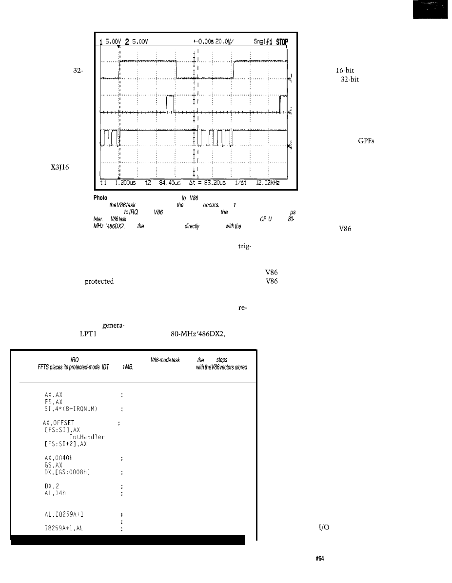
have the luxury of pure
32-bit PM code and
device drivers, you don’t
need V86 mode. For the
rest of us, who want
bit performance without
rewriting BIOS disk
drivers, here’s how it
works.
If you’re looking for
light reading, flip on by.
This column rings the
“most dense writing”
bell and ranks up there
with C++ folks explain-
ing the latest
and
WG31 inventions. If it
were easy, it’d be done
now!
3 5v
Pk
q
q
q
l-Relaying a hardware interrupt a
task requires more time than you’d expect,
MYSTERIOUS GAPS
We’ve
measured
interrupt response time
even if
is executing when interrupt
Trace shows fhe pulse-generator
signal applied
7. The
interrupt handler produces blip in Trace 2 more than 50
The
produces fhe pulses in Trace 3 when if’s not interrupted. The is an
so response time isn’t
comparable
results shown previously.
under a variety of condi-
tions (INK 50 and 57). The latency,
which is the delay from an interrupt
signal to the start of its handler, is
typically a few tens of microseconds,
even when performing a
mode task switch.
in the top trace. Each rising edge
gers a V86 interrupt handler which, in
turn, blips the output port pin shown
in the middle trace.
Horrid as it may seem, waking up
the V86 interrupt handler requires over
other duties, the V86 monitor must
handle hardware interrupts. Those
mysterious gaps in Photo 1 show the
monitor in action, mediating the
code’s access to the outside world.
An obvious tradeoff rears its ugly
head: don’t plan on high-speed inter-
rupts with V86 mode handlers.
With that in mind, Photo 1 may
50 us. It runs for a mere 8 us, then 20
come as a surprise. A V86 task created
us passes before the square wave
the bottom trace by toggling a parallel
sumes. These times are even more
port bit. The output of a pulse
surprising when you realize that the
tor applied to pin 10 of
appears
CPU is an
not the
Listing l--Setting up an
7 interrupt handler within a
requires same
as in real
mode.
above
eliminating any conflict
near address zero.
XOR
aim at int vector
MOV
MOV
. ..using real-mode values!
MOV
IntHandler insert our handler
MOV
MOV AX,SEG
MOV
MOV
MOV
MOV
ADD
MOV
OUT DX,AL
BIOS data segment
pick up port base address
aim at control port
enable int, raise control pins
IN
AND AL,NOT INTMASK
OUT
read mask register
0 = enable interrupt
shazam!
33-MHz ‘386SX starring
in my earlier columns.
Last month, the V86
task required two rou-
tines: the
V86 code
itself and a
pro-
tected-mode V86 moni-
tor. The V86 code runs
much as it does in real
mode and remains bliss-
fully unaware that the
monitor is active. The
monitor handles
and other protection
exceptions produced
when the 16-bit code
attempts to execute priv-
ileged or forbidden in-
structions.
All that protection
makes little sense if an
external interrupt can go
directly to
code.
Thus, in addition to its
FAMILIAR SURROUNDINGS
A V86 task activates an external
interrupt in the usual way: install the
handler’s vector address, tweak the
8259 controller, and enable the I/O
hardware’s interrupt line. Listing 1, an
excerpt from the complete code avail-
able on the BBS, should be entirely
familiar from your real-mode experi-
ences. The behind-the-scenes tricks
(the ones that don’t show up in the
listing) bear some examination.
Remember that the FFTS task
setup code loads the task’s I/O permis-
sion bitmap with zeros, thus granting
unlimited access to all I/O ports. A
more defensive system limits access to
only a few, carefully chosen ports. The
GPF resulting from an attempt to
touch a prohibited port would probably
terminate the task to prevent interfer-
ence with the rest of the system.
The V86 monitor can even restrict
access to specific
bits by setting
the I/O permission bit for that port.
Circuit Cellar INK@
Issue
November 1995
55
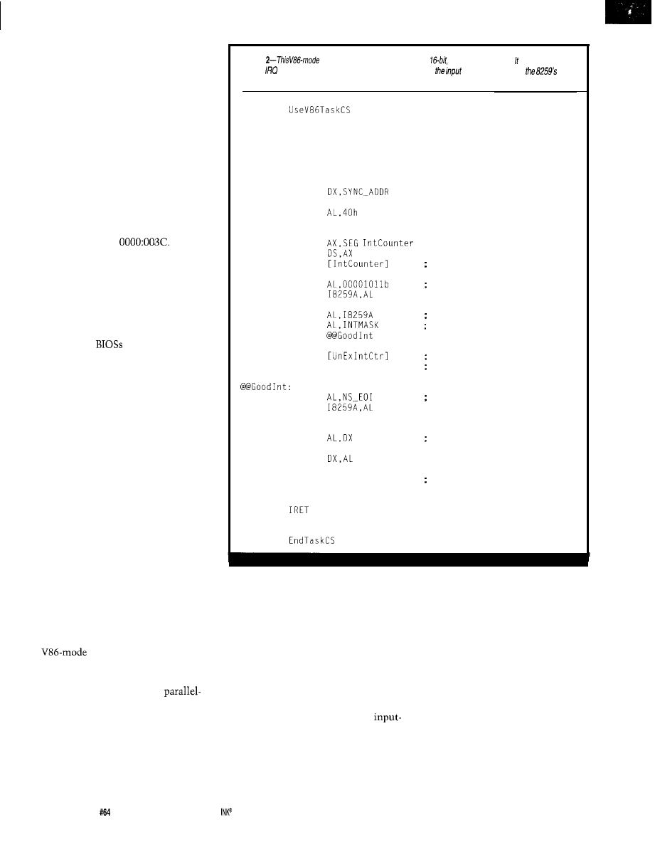
When the task attempts to read or
write the port, the monitor can exam-
ine the offending instruction and ei-
ther supply the actual I/O port value or
make up whatever it likes before re-
suming the task. We won’t get into
that level of detail, but it’s just a (not
quite so) simple matter of software.
As far as the V86 code knows, it
reads and writes I/O ports as usual.
Because of our lax setup, the instruc-
tions execute normally and don’t cause
any additional overhead. Whew!
The V86 code installs the address
of its IRQ 7 interrupt handler in the
vector at address
Unlike
standard real-mode code, it doesn’t
need to save the existing interrupt
vector because the task never ends and
doesn’t pass control to the old handler.
FFTS boots directly after the BIOS
setup, which means the default han-
dler is a simple
I RET
buried in the
BIOS. Some
include a snippet of
code that disables the offending inter-
rupt input line, which isn’t particu-
larly useful in our situation.
In both real and V86 modes, the
256 interrupt vectors form a table of
four-byte entries starting at address
OOOO:OOOO. The CPU’s memory-paging
hardware can relocate each V86 task’s
addresses to separate locations in phys-
ical memory. Because we haven’t acti-
vated that hardware yet, the code in
Listing 1 changes the contents of RAM
near physical address zero.
In protected mode, the CPU uses
eight-byte interrupt descriptors located
in the IDT. The Interrupt Table Regis-
ter specifies both the starting address
and size of the IDT, which can reside
anywhere in storage and may have
fewer than 256 entries. The FFTS set-
up code creates an IDT above the l-MB
line and, thus, prevents conflict be-
tween the protected-mode IDT and the
interrupt vectors.
After its simple setup, the V86
code enters an endless loop. Each pass
around the loop toggles the
port bit that creates the bottom trace
in Photo 1. We’ll look at the loop in
more detail next month, since it holds
the key to a subtle problem.
The PC’s interrupt hardware
doesn’t know about real or protected
modes. When a rising edge appears on
Listing
interrupt handler uses familiar
real-mode techniques. counts bofh
normal
7 interrupts and default interrupts fhaf occur when
signal doesn’t meet
timing specs.
PROC
IntHandler
PUBLIC
IntHandler
PUSH
PUSH
PUSH
MOV
IN
OR
OUT
MOV
MOV
INC
MOV
OUT
IN
TEST
JNZ
INC
JMP
MOV
OUT
@@Done:
IN
AND
OUT
POP
POP
POP
ENDP
AX
DX
DS
AL,DX
DX.AL
@ D o n e
AL,NOT 40h
DS
DX
AX
IntHandler
save bystanders
send a blip
aim seg reg at our data
count this interrupt
write OCW3 to read ISR
is it a valid interrupt?
ISR bit = 1 is normal
ISR bit = 0 means default int
skip EOI command!
reset the controller
remove blip
restore bystanders
the parallel port’s -ACK line, the 8259
generates an interrupt request. As far
as the V86 code is concerned, the in-
terrupt handler shown in Listing 2 gets
control precisely as it would in real
mode.
The handler pulses a bit on the
parallel port, ticks a counter, and then
determines whether the 8259 issued a
valid IRQ 7 interrupt or a default inter-
rupt. The latter occurs when the
pulse timings don’t meet the 8259’s
specifications. A second counter accu-
mulates their occurrence.
As you might expect, the handler
sends an EO I to the 8259 controller on
each valid interrupt, restores the CPU
registers, and executes an I RET that
returns to the mainline V86 code. Just
by looking at the code, you can’t tell
when or where the V86 monitor gains
control. For that, we must examine the
CPU documentation and pore over the
list of restricted instructions.
Some unfamiliar territory peeks
through Photo l’s mysterious gaps!
SWITCHING MODES
The smallest part of the missing
time occurs while the CPU switches
between V86 and PM operation. With
a little help from the V86 monitor
56
Issue
November 1995
Circuit Cellar
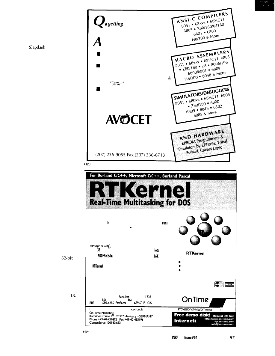
program, this happens automatically at
the beginning and end of the handler.
As with all protected-mode program-
ming, you must map out the whole
process and set up a variety of tables
and code before executing the first
instruction.
style just doesn’t
work any more!
Figure 1 diagrams the CPU’s re-
sponse to an external hardware inter-
rupt during a V86 task. The first step
occurs when the CPU acknowledges
the interrupt and vectors through the
corresponding gate in the IDT. The
sample code this month uses the print-
er port’s IRQ 7 for the sake of conve-
nience, although the principle applies
to any interrupt.
The CPU automatically extracts
the interrupt handler’s code segment,
offset, and privilege level from the
gate’s descriptor. It issues a protection
exception if the handler is less privi-
leged than the interrupted code.
The restriction is more explicit for
V86 mode. Handlers for any interrupts
that may occur when the CPU is in
V86 mode must run in Ring 0 because
the I RET instruction cannot set the
VM bit if it’s executed at any lower
privilege. This means you can get out
of, but not into, V86 mode. So, unless
you disable interrupts in V86 mode,
your handlers are kernel routines.
Because our V86 task, like all V86
tasks, runs with the least privilege, the
CPU automatically switches stacks to
the Ring-O SS:ESP defined in the task’s
TSS. It pushes a variety of information
on the stack, including the address of
the interrupted instruction. This pro-
cess is similar to the stack switch
caused when the CPU handles a GPF.
Now we get to the heart of the
matter. The V86 monitor transfers the
instruction’s address from the
stack to the V86 stack, simulating
what the CPU would automatically do
in real mode. It also extracts the 16-bit
interrupt handler’s address from the
task’s vector table and inserts it in the
Ring-O stack. An I RET instruction
returns to V86 mode and starts the
bit interrupt handler.
Pay attention! There are two inter-
rupt handlers in motion. The PM han-
dler gains control through the IDT
using the CPU’s hardware. The V86
How do you know you’re
the most from your
development tool purchase?
Compare Avocet Systems
l
with the competition.
A Broad Line of High-Quality
Products at Competitive Prices
Free On-Line Technical Support
for Registered Users. No Voicemail!
n
Attractive Multi-User Discount Prices
Our
Educational Discount Plan
Unconditional 30-Day
Money-Back-Guarantee
Now call the obvious choice!
SYSTEMS; I NC.
The Best Source for Quality
Embedded System Tools
( 8 0 0 ) 4 4 8 - 8 5 0 0
RTKernel is a
professional, high-performance,
real-time
multitasking system for MS-DOS and Embedded
Systems.
can use
DOS device drivers and BIOS, and
other DOS applications as a task even Windows!
RTKernel is
loaded with features:
an
unlimited
number of tasks, excellent performance, a full set of inter-task
communication functions (semaphores, mailboxes, synchronous
real and protected mode support, drivers for
up to COM ports and Novell’s IPX services, and
more...
It’s
and very compact (about code,
6K data), making it ideally suited for Embedded Systems.
is well-documented and easy to use. All hardware
drivers always come with source code; kernel source code
available at extra charge. No run-time royalties.
Join thousands of satisfied customers!
In North America,
please contact:
On Time Marketing
U s e
f o r :
l
process control
d a t a a c q u i s i t i o n
88 Christian Avenue
New York
USA
Phone (5
689-6654 Fax (S
689-I I72
r e a l - t i m e s i m u l a t i o n s
b a c k g r o u n d p r o c e s s i n g
Libraries: $495
Source
Code:
add $445
(516)
(516)
73313.3177
From other countries, please
M A R K E T I N G
Tools
Circuit
Cellar
November 1995
handler gains control after the monitor
of reporting protected-mode excep-
twiddles its stack.
tions.
The next step in Figure occurs
when the 16-bit interrupt handler
attempts to execute an I RET. In V86
mode, I RET is a privileged instruction
that causes an immediate GPF and
invokes the V86 monitor using the
same mechanism we explored last
month. Once again, the CPU switches
to 32-bit, Ring-O code and pushes the
V86 state on the stack.
The FFTS start-up code repro-
grams the 8259 to generate Int
which are the more-or-less standard
interrupts used by other
mode systems. IRQ 7 thus produces
Int 57 rather than Int OF. Keeping this
straight can be a challenge, but the
payoff is worth it.
At this point, the V86 mode stack
should hold the same return address
that the monitor created when it han-
dled the interrupt. The monitor recov-
ers that address, inserts it in the Ring 0
stack, and executes another I RET to
return to V86 mode, only this time it’s
in protected mode. Assuming the V86
code didn’t change the return address
[it can happen!), the CPU resumes
execution at the interrupted instruc-
tion as it would in real mode.
Pop quiz: if the CPU automati-
cally responds to Int 57, which inter-
rupt does the V86 code see?
Answer: anything is possible when
the
monitor shuffles the stack!
Anatomyofa
Great Frame Grabber
As you trace through Figure 1, you
can see why interrupt latency can be a
big problem in
code. The
V86 monitor gets involved in two
places, simulating both the interrupt
and the subsequent I RET. Although
RISC proponents argue that simple
instructions are faster than complex
instructions, it remains true that ex-
ecuting a vast number of teensy in-
structions still takes more time than
running a few husky ones.
Low Price
Forget
priced on-board
What’s in those mysterious gaps?
Looks like PM code to me!
NUMERIC RELATIONS
The interrupt that starts this pro-
cess could come from any of the usual
sources. I used the parallel port with
its access for a pulse generator or a
push-button switch. This is one of the
few cases where contact bounce isn’t
much of a problem. Even though the
code is slow by previous standards, it’s
still faster than a button.
Call and find out how
quality products, responsive technical
and elegant software get
your application quickly to market.
The
printer-port interrupt
normally drives the IRQ 7 line. I’ll
leave the pathological case of
with IRQ 5 as an exercise for you. The
system board’s primary 8259 interrupt
controller handles IRQ 0-IRQ 7, which
normally invokes the handlers for Int
OF. Unfortunately, those inter-
rupts conflict with the CPU’s method
Vision Requires Imagination’”
l-800-366-91 31
l
Phone:
l
Fox:
Homepage:
Box 276, Beaverton, OR
The structure in Listing 3 defines
the relations built into FFTS. The first
row represents IRQ 0 and the last is
IRQ 15. As in real mode, IRQ 2 cannot
occur because the secondary 8259
chains its output into the master 8259
through that signal. Including a row
for IRQ 2 simplifies the table access
code and costs a mere eight bytes.
The first two columns give the
PM and V86 interrupt numbers which
correspond to each IRQ line. The PM
column uses the same constants that
the FFTS set-up routine loads into the
8259 controller. The V86 column
Precision
5 8
November
1995
Circuit Cellar
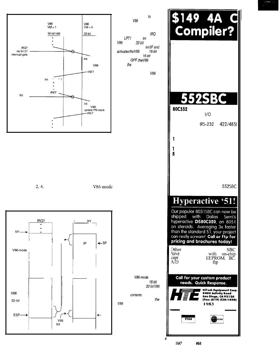
demo
monitor
Ring 3
Ring 0
PM
57 handler
fetch V86 vector
update
stack
update PM stack
OF handler
OD
GPF
OD handler
fetch
stack
plays the familiar real-mode values.
Unlike genuine real mode, there is no
conflict with the CPU’s reserved inter-
rupts: the V86 monitor creates these.
The third column merely pads
each table entry to exactly eight bytes.
The ‘386 CPU’s scaled addressing
mode simplifies access to tables with
entries that are
or 8 bytes long.
It’s a CISC thing.
The fourth column holds the off-
set of the PM interrupt handler for
unused
G S
FS
DS
ES
s s
ESP
EFLAGS
c s
EIP
OF
vector
Figure I-Responding an
interrupt in
mode requires
firmware coordinated with the
CPU’s hardware. Here, the
process begins when an
7
from
triggers 57. The
monitor’s
interrupt
handler simulates an
task’s
handler. When the
IRE T
triggers a
monitor
adjusts stacks to simulate a
normal IRE T and returns
control to the interrupted
instruction.
each interrupt. Each
entry point is a short
stub that executes the
P
U S HA
described
above, then loads AL
with its IRQ number.
The FFTS set-up code
creates an interrupt
gate for each interrupt
using the values in this column.
Obviously, the interrupt number
pairs are arbitrary. Each pair represents
several promises that you must fulfill
while writing the rest of the code. The
8259 interrupt controllers must emit
the PM interrupt number, the V86
code must prepare for interrupts using
the
numbers, and the V86
monitor must match them up cor-
rectly. That’s a lot of “must” with no
automated checking.
Just after
unused
stack
1 B-bit code
monitor
stack
code
Just before
simulated
OF
FLAGS
c s
unused
G S
FS
D S
E S
s s
ESP
EFLAGS
c s
EIP
ESP
You need not put
this information in a
table. Burying it in
special-purpose han-
dlers can produce
somewhat faster code
at the expense of easy
maintenance. Once
you see what’s going
on, just tune things to
match your needs.
Figure 2-A
task
has two stacks: one for
code and one for the
monitor. This diagram shows
the stack
just after an
interrupt occurs (i.e., before
monitor activates the lb-bit
interrupt handler). The monitor
simulates real-mode CPU
action by copying the
interrupted instruction’s
address from the Ring-0 stack
to the Ring-3 stack.
You heard right! A quality K&R C
compiler designed for the 8051
microcontroller family, just $149,
including the Intel compatible
assembler and linker. A source
level simulator is also available for
just $169. A great companion to
our fine Single Board Computers,
like those below. CALL NOW!
a ‘5 1 Compatible Micro
40 Bits of Digital
8 Channels of 10 Bit A/D
3 Serial Ports
or
2 Pulse Width Modulation Outputs
6 Capture/Compare Inputs
Real Time Clock
64K bytes Static RAM
+ UVPROM Socket
12 bytes of Serial EEPROM
1 Watchdog
1 Power Fail Interrupt
1 On-Board Power Regulation
1 Expansion Bus
Priced at just $229 in 100 piece
quantities. Call about our
C Development Kit, just $499 qty 1.
versions of the 8031
processors
:a ture registers,
and more. Call or for’a list!
8031SBC as low as $49
Since
(619) 566-1892
Internet e-mail: info@hte.com
Internet ftp: ftp.hte.com
123
Circuit Cellar
issue
November 1995
5 9
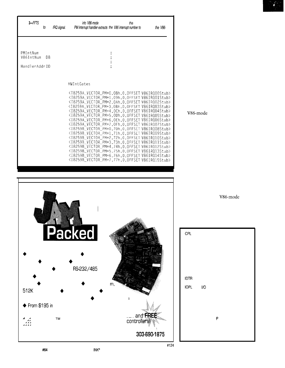
Listing
maps external
hardware interrupts
interrupts using array. Each row
corresponds an
The
locate
mode vector in real-mode storage.
STRUC
HWGATEMAP
D B
?
Int number in PM mode
?
Int number in V86 mode
DW
?
pad to dword boundary
?
offset of handler stub
ENDS
HWGATEMAP
LABEL
DWORD
HWGATEMAP
HWGATEMAP
HWGATEMAP
HWGATEMAP
HWGATEMAP
HWGATEMAP
HWGATEMAP
HWGATEMAP
HWGATEMAP
HWGATEMAP
HWGATEMAP
HWGATEMAP
HWGATEMAP
HWGATEMAP
HWGATEMAP
HWGATEMAP
Embedded
Controllers
A/D inputs, 12-bit accuracy Analog
outputs Relay control Counter/Quadrature
encoder inputs Buffered
serial
ports Operator interface via keypad and LCD
display Program using a PC 512K progra
data memory 5V only operation Built-in
BASIC supports all on-card hardware Floating point math
l ’ s
REMOTE
Call
for more information
PROCESSING
catalog of embedded
The embedded control company
Ph: 303-690-1588, Fax:
SAVING THE STATE
The CPU stores the information
required to resume the interrupted
instruction on a stack, regardless of
whether the CPU was in real or pro-
tected mode. In V86 mode, however,
the state information winds up on a
Ring-O stack that is inaccessible to
Ring-3 code. The V86 monitor, run-
ning in Ring 0, adjusts both stacks
before activating the 16-bit interrupt
handler and readjusts them on return.
The left-hand diagrams in Figure 2
show the two stacks after the IRQ 7
occurs (just before the CPU enters the
V86 monitor program). The right-hand
diagrams show the adjusted layouts.
tasks generate address-
es using the familiar seg:off method,
with segment registers holding the
high-order 16 bits of the 20-bit address.
The address bit patterns in the seg-
ment registers are generally not valid
protected-mode selectors. As you
should know by now, a protection
exception occurs very quickly should
the CPU enter protected mode with
bad segment registers.
Once you have a CISC CPU,
though, a little more complexity is no
big deal. After the CPU acknowledges
the external interrupt and switches
stacks, it pushes the
con-
tents of DS, ES, FS, and GS onto the
Ring-O stack and fills the registers
with zeros. An all-zero selector corre-
sponds to the null descriptor entry in
Current Privilege Level
DPL
Descriptor Privilege Level
EOI
End Of Interrupt (command)
FDB
Firmware Development Board
FFTS
Firmware Furnace Task Switcher
GDT
Global Descriptor Table
GDTR
GDT Register
GPF
General Protection Fault
IBF
Input Buffer Full
IDT
Interrupt Descriptor Table
Interrupt Descriptor Table Register
IF
Interrupt Flag
Privilege Level
LDT
Local Descriptor Table
LDTR
LDT Register
NT
Nested Task
OBF
Output Buffer Full
P bit
Present bit (in a PM descriptor)
RF
Resume Flag
RPL
Requestor rivilege Level
TF
Trap Flag
TR
Task Register
TSS
Task State Segment
VM
Virtual Machine (in EFLAGS)
60
Issue
November 1995
Circuit Cellar
GDT[O],
which means the zeroed regis-
ters won’t trigger any errors.
The CPU next pushes the V86
SS:ESP onto the stack. Obviously,
there is something
going on
here because the CPU pushes these
values onto the Ring-O stack using a
selector before entering the
mode handler. These are complicated
instructions, indeed. As you become
more familiar with protected-mode
programming, you begin to appreciate
what CISC really means.
The next three stack entries are
the EFLAGS and CS:EIP values. The
VM bit in the EFLAGS stack entry is 1
because the CPU was in V86 mode
when the interrupt occurred. The CPU
clears VM in the EFLAGS register
before starting the interrupt handler,
which is why the handler is a 32-bit
PM routine instead of 16-bit V86 code.
The CPU stores a
value for
EIP. The high-order 16 bits of the
bit EIP register almost always is zero
in a
task. The exception
occurs when the program executes
code in the 64 KB just beyond the
MB line. I ignore that possibility-our
code wouldn’t think of doing such a
thing. If you must run real DOS pro-
grams in a V86 box, this is just one of
the headaches you’ll encounter.
With that out of the way, the CPU
fetches and executes the
first
instruction. Next month you’ll see the
FFTS handler begins with a PUSH A that
saves the remaining CPU registers on
the stack, producing the structure in
Listing 3. Since the stack grows down-
ward in memory, 01
is the first
value pushed on the stack and 0 1 d ED I
is
the last. Each segment register value
has 16 high-order zeros to keep ESP
aligned on four-byte addresses.
All the stack shuffling before the
happens automagically in the
first few microseconds after the port’s
IRQ line goes active. What follows
soaks up the remainder of that myste-
rious
gap: faking a real-mode
hardware interrupt.
RELEASE NOTES
The code this month pokes three
characters into the bottom-right corner
of the video buffer. The first character
changes after each 256 V86 task
switches, the second increments on
valid IRQ 7 interrupts, and the third
tallies default interrupts caused by
invalid timing. A signal applied to
-ACK (pin 10) triggers the
interrupts.
You can drive pin 10 with a push
button or signal generator. If you crank
the frequency high enough, you’ll see
some default IRQ 7 interrupts.
Next month, we’ll fill in those
gaps with straightforward code.
q
Ed Nisley
as Nisley Micro
Engineering, makes small computers
do amazing things. He’s also a
member of Circuit Cellar INK’s
engineering staff. You may reach him
at
or
413
Very Useful
414
Moderately Useful
415 Not Useful
One of
Micromint’s hottest-selling products for the past five years
has been the
stackable controller. It has been a leading price/per-
formance choice among our customers. With our new RTC320 board, we
have expanded the value of that relationship even more.
Occupying the same small
RTC footprint and using S-V-only
power, the
uses the new Dallas Semiconductor
which is
8031 code compatible and 3-5 times faster. At 33 MHz, the RTC320 is an
controller! Along with the new powerful processor, the RTC320 board
accommodates up to 192 KB of memory, two serial ports (RS-232 and
24 bits of
parallel
and a
ADC. The RTC320 puts
some real firepower under the abundant variety of RTC I/O expansion boards.
Plugging in your favorite ICE or EPROM
emulator is the easiest way to develop
code. For the diehards who like to twiddle
the bits directly, we have a ROM monitor
specifically designed for the Dallas ‘320.
(22 MHz)
(Call for
on 33 MHz)
4
PARK STREET VERNON, CT 06066 (860)
l
FAX (860)
Circuit Cellar INK”
Issue
November 1995
61
Those who have X- 10 modules
installed in their home know that
what sounds like a great idea isn’t
perfect. X-10 is inherently a one-way
system. Attempting to jump from one
phase to another or noise on the line
can sometimes keep transmissions
from getting through. Without feed-
back, you have no way of knowing
that the command was lost.
It’s not that I hate X-IO. I don’t. In
fact, if not for it, we may not have
progressed to this stage of home auto-
mation. Although X-10 has put the
facilities in their standard to allow
bidirectional communication and data
passing, very few devices currently
support it.
A big break came for many manu-
facturers with the
13 line interface
which lets us safely interface our com-
puters to the line and send X-10 com-
mands.
13 enabled third-party
equipment to use X-10 modules.
When the TW523 module was
released, we thought two-way commu-
nication was finally here. But, the
command for sending extended data is
not recognized by even the TW523, so
using the power line as a data-passing
medium was still not at hand.
Jeff Bachiochi
Carrier Current Modem
Part 1: Communicating at
1200 bps Around the House
f you count only
the PCs that are
turned on at least
once a week at my house,
you get five. I own the slowest, an
8088 portable which still gets used for
writing this monthly column. Ryan,
now a senior in high school, has the
fastest machine. (He swaps mother-
boards the way used to trade baseball
cards. No telling what speed he’s cur-
rently running!)
The machines have two things in
common, though. They all have their
own assortment of games (ugh) and a
word processor. Although PCs abound,
printers do not, and we all need to
print. If we were tied together, print
files could easily be moved to the print
station without stringing more wires
around. Wouldn’t it be nice if we could
use wiring already in place throughout
the house? How about the power line?
Although this month’s project
starts out to solve this problem, it
morphs into a different animal.
POWER-LINE STANDARDS
Ken has kept us up-to-date on the
committee’s work toward na-
tional standards for home automation.
I think it’s interesting to note that the
old and outdated X-10 “standard” still
used by many today remains a hurdle
in gaining a new standard.
X-l 0 PROTOCOL
First, let’s have a quick overview
of the X-10 protocol.
By sending three 1-ms bursts of a
tone, a binary 1 bit is indi-
cated. The bursts occur at the 0, 60,
and 120” points of the
wave.
The transmission is followed by an
absence of bursts in the second half
cycle. Binary 0 bits send no bursts for
the first half cycle and
bursts for
the second half cycle at the 180,240,
and 300” points.
The preamble doesn’t use quite
the same format, so it isn’t confused as
data. However, for an overview, just
remember data is transmitted in
bursts of
carrier (or lack of).
CEBUS’S PLBUS
In INK 15, Ken’s
Update”
touched on most of the media pro-
posed in that standard. Special atten-
tion was given to power-line proposals.
The data protocol then looked an aw-
ful lot like the X-10 protocol.
62
Issue
November 1995
Circuit Cellar
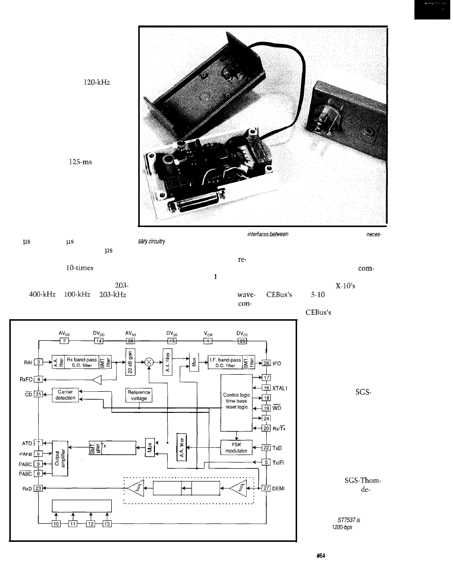
There were some major differ-
ences, however. Binary data was differ-
entiated by time: 1 ms for a 1 and 2 ms
for a 0. Bit times alternately measured
the time the carrier was on with the
next bit measured by the duration the
carrier was off. Again, a
car-
rier was used but bits did
not
have to
begin on zero crossings.
Besides the fact that a CEBus sig-
nal could completely swamp an X-10
transmission, a CEBus signal, with the
correct data pattern, could look to
X-10 modules like a legal signal. To
prevent this from happening, CEBus
intended to place a
null signal
in its transmissions which lasted over
158 ms. Talk about lowering through-
put!
Fortunately, the CEBus committee
revised its proposal. In 1994, an up-
dated proposal was documented. Here
are some highlights.
Data bit timing was redefined as
100 for a 1,200 for a 0,300 us for
an end of frame (EOF), and 400 for
an end of packet (EOP). These timing
changes brought a
improve-
ment in data throughput.
The carrier was redefined as a
Hz to
to
to
linear sweep, taking 100 us. Longer
Photo 1-SGS-Thomson’s power-line modem chip
the AC line and a serial port. All the
is crammed into a OKW Hammond plastic enclosure.
gether on the power line
and give us the best of
both worlds.
XTAL2
SGS-THOMSON
data, such as a 0, EOF, and EOP,
secutive bit, bringing about a complete
quire multiple sweeps since the basic
change in strategy and circuit
sweep time is equal to a bit. Instead
plexity!
of alternating the carrier on and off for
So, we jump from
60 bps to
consecutive data bits, the swept
latest
kbps. The X-10
form’s phase is inverted for each
system is certainly simple and slow.
implementation,
although complex, is
much quicker. It looks
like they can reside to-
MCLK
RSTO
Where does
Thomson fit into the
picture?
The European com-
munity has been engaged
in developing a consumer
band-pass
S.C. filter
Post demo
S.C. filter
Correlator
market as part of the
ESPRIT project (now
called European Home
Systems) on domestic
automation.
son’s ST7538 was
FSK demodulator
Test logic
Test1 Test2 Test3 Test4
Figure l--The
a complete
half-duplex,
power-line
modem on a chip.
Circuit Cellar INK@
Issue
November 1995
63
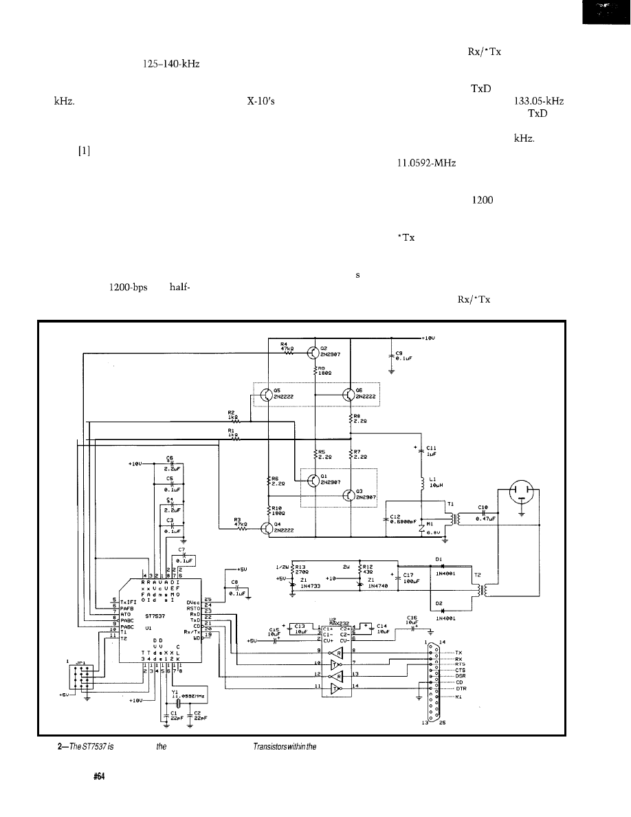
signed specifically for this purpose. It
complies with Europe’s CENELEC EN
50065 standard by using
carriers for home automation and the
FCC with carrier frequencies less than
450
SGS-Thomson chose FSK
because “Among the alternatives, ASK
is too susceptible to noise, and spread
spectrum requires complex and costly
circuits.”
While SGS-Thomson’s approach is
not the fastest or state-of-the-art, it is
the quickest and cheapest to imple-
ment. A power-line modem can be
used to transfer data between two
computers over existing wiring. It’s
not 28.8 or 19.2 kbps, but on the other
hand, you don’t have to pay for the call
either. Oh yeah, one more thing-it
won’t false trigger your X-10 modules.
The ST7537
FSK
duplex modem interfaces between a
microcontroller’s serial port and do-
mestic power lines. Unlike X-10, SGS
places a full-time carrier on the line
during transmissions with no atten-
tion paid to zero crossings. This im-
proves
60-bps throughput rate
to 1200 bps.
Additional benefits are gained
with the ST7537 (see Figure 1). The
reset and watchdog functions keep
your micro on the straight and narrow
even if things slide a bit off center.
The ST7537 requires 10 and 5 V. If
the 10 V drops below 7.6 V, the RSTO
(reset out) pin is driven high for at
least 50 ms. This pin can be used as an
early power-fail warning while the
supply is still high enough to ensure a
stable, regulated 5 V. The watchdog
input must be strobed every 1.5 to
prevent RSTO from spending the next
FOLLOW THE TRANSMIT PATH
Driving the
input-control
line to a logic low places the ST7537
in transmit mode. Data to be transmit-
ted goes into the
input pin. An
FSK modulator generates a
carrier when the input data at
is
low. When the data is high, the FSK
modulator shifts to 131.85
These
frequencies are achieved from the
crystal attached to the
ST7537, so they remain precise (100
ppm). The modulator can switch fre-
quencies at up to
bps.
the line if the
control gets
The user may drop out of transmit
mode at any time by raising the Rx/
control input. Transmit mode is
automatically suspended after 1 s. This
feature is part of the European Home
Systems protocol and can be disabled.
It prevents a transmitter from tying up
50 ms high.
Figure
at the core of power-he modem interface.
doffed lines are thermally coupled.
64
Issue
November 1995
Circuit Cellar INK@
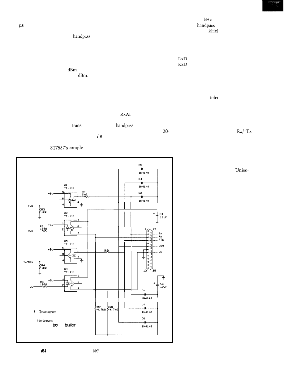
hung low. It must be returned high for
2 before reenabling the transmitter.
The modulated signal then passes
through a switched-capacitor
filter to remove much of the harmonic
content. This step is important to the
internal processing of the ST7537
since the final spectral output must
pass FCC limits. Second-harmonic
distortion is reduced by 50
and
third-harmonic distortion by 60
former which couples the carrier to the
power line.
Bias to the push-pull transistors is
controlled by the
Finally, an output amplifier drives
external push-pull transistors from the
AT0 [analog-transmit output). The
final output stage is fed back into the
ST7537 PAFB (power-amplifier feed-
back) input to keep the output under
control. The push-pull’s output drives
a winding of the tank circuit. The tank
circuit is part of an isolation
mentary outputs PABC and
l
PABC
(power-amplifier bias control). When
the ST7537 exits the transmit mode,
these outputs remove the bias from
the push-pull transistors, leaving them
in a high-impedance state so they
don’t load down the tank.
FOLLOW THE RECEIVE PATH
one in the transmit section) and a
The ST7537 spends most of its
time in receive mode, looking for carri-
ers to detect. The output transistors
amplification stage.
don’t impose any significant load on
the tank circuit. Therefore, the ST7537
A local oscillator driven by the
can listen for a carrier coupled through
the isolation transformer from the
crystal then converts the amplified
line. These signals enter the ST7537
through the
(receive-analog in-
put). They pass through a switched-
capacitor
filter (similar to the
I
RI
Figure
can be used to
create an isolation barrier between the
power-line
your PC. Some
optocouplers may be slow
high-speed serial communications,
however, so choose carefully.
carrier to 5.4
A second switched-
capacitor
filter (this time
centered on 5.4
improves the
signal-to-noise ratio, and the carrier is
demodulated.
Provided the *CD (carrier-detect)
output is low, data is available at the
output. While *CD is high, the
output is held high (idle). *CD
proclaims the carrier status about 6 ms
after the carrier has actually been de-
tected or lost. This delay allows short
carrier absences and noise to be over-
looked.
Similar to a
modem, the
power-line modem connects to an
available RS-232 serial port on your
favorite PC (refer to Photo
1
and Figure
2). Four connections are made: TXD,
RXD, DCD, and RTS. RTS is used by
the PC to place the ST7537 in
mode, which determines the direction
of the data.
In converting TTL to RS-232, you
can use a MAX232 with the ST7537. If
the MAX232 is powered by an isolated
source, it provides sufficient protec-
tion for the PC from the line.
lated power supplies referenced to one
side of the line can damage your PC.
The computer’s interface must be
isolated via optocouplers to prevent
damage from occurring. Figure 3 shows
how optocouplers can be used to estab-
lish an isolation barrier between the
ST7537 and your PC.
It is necessary to use a communi-
cations program which lowers the RTS
line when transmission begins and
which raises it to disable the transmit-
ter when listening. If yours doesn’t do
this, take a look at Listing
1.
Here you
can see how you might communicate
between systems using this project’s
hardware. (The software also applies to
those of you who wish to interface
your PC to an RS-485 network. The
RTS signal can control the DE pin on
75 176 RS-485 bus drivers.)
Connected systems act as slaves,
monitoring for messages until a key is
pressed. A key press lets the program
know you wish to send a message to
another node. The program prompts
for a message and node address and
checks to see if the bus is in use by
testing the carrier detect from the
ST7537. If it’s free, raising the RTS
66
Issue
November 1995
Circuit Cellar
Listing l--This
demonstrates the framework for a
of communicating
PCs.
1 0
2 0
30
4 0
50
60
70
8 0
90
100
110
120
130
140
150
160
1 7 0
180
190
2 0 0
2 1 0
230
2 4 0
2 5 0
2 6 0
2 7 0
SCREEN
WIDTH 80
KEY OFF: CLS: CLOSE
DEFINT A-Z
OUT
AND
the address of this node
IF
OR
THEN GOT0 40
a
IF
OR
THEN GOT0 70
IF BASE = 1 GOT0 120
AS
GOT0 130
AS
OUTPUT AS 2
LOCATE
ON ERROR GOT0 490
GOT0 250
in a string to
the address to send it to
IF
OR
THEN GOT0 180
=
+
+
IF
AND
= THEN
detected
waiting": GOT0 210
to transmit"
OUT BASE + 4,
OR
OUT BASE + 4,
AND
N =
(continued)
line enables the
transmitter,
and the message is sent. Lowering the
RTS line disables the
trans-
mitter (carrier), and the node returns to
slave mode.
a message is received while in
slave mode, the preamble and destina-
tion bytes are checked. If the destina-
tion matches this node’s address, the
message is received, and an acknowl-
edge message is returned to the sender.
the destination matches this node’s
address with the high bit set, this is an
acknowledgment of a previously sent
message. If the destination doesn’t
match the node’s address, the message
is discarded.
The program does not include any
packet protection such as a checksum.
This kind of error trapping is left up to
the user.
NEXT MONTH
Sending messages between com-
puters over the power line probably
does not seem like a big deal. But, stay
tuned. I’ll put some smarts in the node
and try to close the loop on X-10.
in
(44)
Canada: (514)
Australia: (3)
Inquiries Welcome
Odds are that some time during the day you
will stop for a traffic signal, look at a message
display or listen to a recorded announcement
controlled by a Micromint
We’ve
shipped thousands of
to
Check out why they chose the
by
calling us for a data sheet and price list now.
MICROMINT, INC.
4
Park Street, Vernon, CT 06066
(203) 872-2204
Circuit Cellar INK@
Issue November 1995
6 7
Bachiochi (pronounced
AH-key”) is an electrical engineer on
Circuit Cellar INK’s engineering
staff.
His background includes product
design and manufacturing. He may be
reached at
Joel Huloux and Laurent
Power Line
Modem Application,”
Power
Line Modems and Applica-
tions,
SGS-Thomson Micro-
electronics, Application Note
1994.
SGS-Thomson
55 Old Bedford Rd.
Lincoln, MA 01773
(617)
416 Very Useful
417 Moderately Useful
418 Not Useful
Listing
l-continued
280
N = NN: NN =
IF
THEN PRINT "Operator
interrupt": GOT0 170
290
300
310
320
330
340
350
360
370
IF N = NN THEN X = X + 1 ELSE X = 0
IF
AND
= THEN
GOT0 280
IF
THEN GOT0 280
=
FOR X = 1 TO
IF
=
THEN A$ =
GOT0 370
NEXT X
PRINT"Preamble not found--Canceling": GOT0 260
IF
=
THEN
my address": GOT0
400
380
IF
=
THEN
an ACK to
me": GOT0 450
390
not to me Canceling": GOT0 260
400
message to me has been received"
410
420
PRINT"1 will send an acknowledge"
430
=
+
+
+
+
440
450
460
470
480
490
GOT0 210
acknowledgement to my message has been received"
let's wait for more messages"
GOT0 250
RESUME
Introducing
l
Features include:
Brighten From Off
The Complete
Compatible lighting
Control Solution is Here!
Pre-Set Dim
Powerline Control Systems has combined the reliability of hard-
*
Soft-Start
wired systems with the ease of X-10 installation. Our full line of 1000,
200
Dim Levels
1500, and 2000 Watt Lighting Control Modules cover all of your high
power lighting needs at a fraction of the cost of other alternatives.
Advanced
These products are available now through all major Home Automation
Programming
UL Listed
distributors.
is a trademark of X-IO (USA) Inc.
Inductive Load Control Improved Receiving
Remote Operation with
Slave Switches
Memory Solid State
100% Money Back Guarantee Made in the U.S.A.
For
more information about PCS’s
lighting control products call:
68
Issue
November 1995
Circuit Cellar
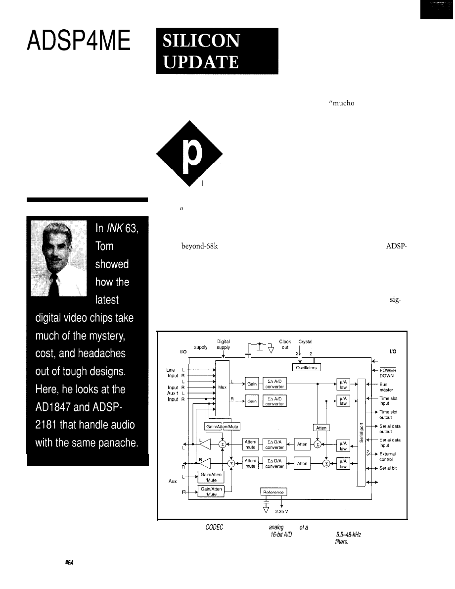
Tom Cantrell
Audio Processor
Chips for the
Masses
ersonalized
license plates take
on the flavor of the
locale. Here, in Silicon
Valley, if you’ve got a vexing design
problem, keep an eye out for “PAL
GURU.
Critical market intelligence can be
gathered with an eagle eye. Remember
back when conjecture raged about
Apple’s
plans? A cruise
through their lot would have revealed
“RISC MAC.”
My favorite is the regally restored
candy man, the “DRAM REP,” deigns
to visit.
One reason the DRAM rep rides in
style is that all the new-fangled multi-
media stuff sucks bits-DRAM, CD,
hard disk, and CPU-like that Rolls
sucks gas. Around here, when folks in
the PC food chain hear “multimedia,”
it sounds like
muy dinero.”
Last month, I covered the basics of
digital video and how the latest chips
take much of the mystery, not to men-
tion cost and design headaches, out of
what were traditionally tough designs.
Since it’s called “multimedia,” not
“unimedia,” now’s a good time to look
at some no-muss-no-fuss wonder chips
that handle the audio side of the mul-
timedia equation with similar pa-
nache.
HEAVY METTLE
Analog Devices splits the audio
work into analog and digital parts, the
AD1847 stereo CODEC and the
218 1 DSP, respectively.
The ‘1847, responsible for analog
I/O, mixing, and code/decode, conveys
Rolls Royce that commands attention,
the digital audio to and from the DSP
not to mention about four of those
via a specialized serial bus. Let’s start
ever-shrinking excuses for parking
with the input jacks and follow a
spaces, wherever it goes. Believe me,
nal through the ‘1847 to see (er, hear)
it’s a big deal when Silicon Valley’s
each function in action.
Analog
Analog
Digital
t
RESET
1
Line 2
Line
output
2
input
clock
Frame
AD1847
sync
Figure l--The AD1847
integrates the entire
portion high-performance audio design onto a
single chip. Features include multiple stereo inputs,
and D/A converters,
sample rate, analog
and digital mixing, programmable gain and interpolation, decimation, and low-pass
70
Issue
November 1995
Circuit Cellar INK’?
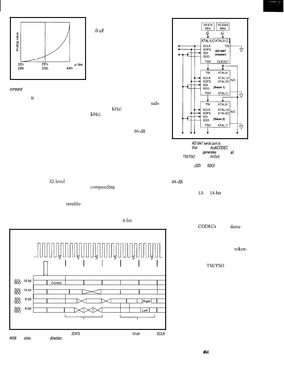
Max
Min
Digital value
8 0 h
A-law
Figure 2-A primary function of a CODEC is to
(compress and expand) fhe digitized audio.
The principle is simple-give away high-magnitude
input resolution increase dynamic range.
Up to four stereo inputs (Line 1,
Line 2, Aux 1, and Aux 2) can be con-
nected to the ‘1847. As shown in Fig-
ure 1, the Line and Aux 1 inputs feed a
multiplexer for selectable presentation
to the A/D converters. Aux 1 can also
be mixed in the analog domain (i.e.,
post-D/A converter) with the output, a
role Aux 2 is limited to. Even if the
D/A converters aren’t outputting any-
thing (i.e., they’re muted), the analog
mixing function works.
converters.
Forget hassling with any
some front-end filter. Thanks to a
combination of 64-times oversampling
followed by low-pass decimation (to
Once past the mux, a pair of amps
applies independent
gain for
the left and right channels which each
proceed to 16-bit (i.e., CD quality) A/D
0.4 times the sampling frequency), the
only external filter components are a
1
capacitor for each channel.
However, to deal with rather loose
definitions of line level (2 V p-p?) in
the audio world, it is recommended to
AC couple the ‘1847 inputs (1 Vp-p)
and outputs (0.7 V p-p], calling for a
few more Rs and Cs.
Speaking of the all-important
sampling frequency, the question is
which one? Featuring a pair of crystals
(typically 24.576 and 16.9344 MHz)
and a programmable divider, the ‘1847
handles more than a dozen sample
rates that cover the range from
phone (5.5
to better than CD (48
The output of the A/D converters
is 16-bit signed PCM (same as CDs)
and offers a whopping
dynamic
range. Note that the 16-bit PCM data
is also made available for on-chip mix-
ing, this time in the digital realm.
the A/D conversion by devoting more
codes to low-amplitude inputs.
The result is more dynamic range
with the same number of bits. For
example, simple
unsigned PCM
Onto the “CO” part of “CODEC,”
where the linear 16-bit PCM is com-
pressed to 8 bits using the telecommu-
nications-inspired A-law (Europe) and
u-law (USA, Japan) standards. As you
can see in Figure 2, these so-called
(i.e., compress and ex-
pand) schemes effectively nonlinearize
Time slot 0
Time slot 1
Time slot 2 Time slot 3 Time slot 4
Time slot 5
SCLK
SDFS
stereo
mono
Right
Status
Left
Right
Control Left
Status
Left Left
stereo
Control
Left
Right
Status Left 0
o
mono
C o n t r o l Left
Status
Left
0
0
Playback
Capture
Figure 4-The AD1847 transfers a frame (the
pin signals frame sync) containing six
(clocked by
first)
three in each
Figure 3-The
an on-ramp to an
audio highway
supports
designs. A
single-master CODEC
clocks for slaves
and the
(Time Slot
daisy-chain controls
access. In this so-called one-wire configuration, the
input and output
and
pins are tied together.
The coded digital data is passed on
to the serial port, which is a rather
(a format the ‘1847 also supports) has a
range while A-law and u-law
innocuous name for what’s actually an
achieve 64 and 72 db, respectively (the
equivalent of
or
PCM).
elegant time-division-multiplexing
(TDM) packet LAN for audio.
Multiple
can be
chained (see Figure 3) with the master
(BM pin high) responsible for generat-
ing the serial clock (SCLK) and frame
sync (SDFS) for the slave(s). The
passing-like arbitration scheme hands
control from the master to each slave
via daisy-chained
(Time Slot
In/Out) pins.
As you can see in Figure 4, this is
a so-called single-wire setup, in which
the data in and out pins (SDI, SDO) are
tied together. This configuration as-
signs six 16-bit slots-three in each
direction-to each CODEC, while a
two-wire variant that doubles band-
width (i.e., three slots) is also sup-
ported.
Incoming digital data goes through
more or less the reverse process-de-
coding (the “DEC” part of “CODEC”)
Circuit Cellar INK@
Issue
November 1995
7 1
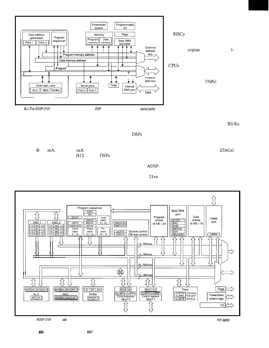
memory data
Data memory data
A D S P - 2 1 0 0 b a s e
architecture
b u s
Figure
combines a high-speed (33 MIPS)
core with CODEC-compatible
(SPORT) and a whopping 80 KB of on-chip RAM.
to 16-bit PCM and D/A conversion
with some extra filtering and program-
mable (64-level) attenuation stages
along the way.
all those sound bytes flying to and fro.
Consuming little board space,
power (5 V 140
less than 1
in power-down mode), and bucks
in low volume), the AD 1847 easily
dispatches with all the analog hassles.
Now, it’s simply a matter of figuring
out what to do (and how to do it) with
RISC MEETS 8051
When it comes to the never-end-
ing architecture wars,
don’t get
the attention of their more glamerous
desktop RISC and CISC brethren. But,
look under the hood, and you’ll find
that
are just as whizzy in their
own purposeful way.
family, whose members combine a
As shown in Figure 5, the
2 18 1 ($54 in low volume) is the latest
member in the Analog Devices
common DSP core with chip-specific
memory and I/O.
The ‘218 1 does exhibit a number
of
characteristics including
pipelining, high-clock rate (33 MHz),
single-cycle execution of most instruc-
tions, and
(80 KB!) on-chip
clock memory.
A key difference with desktop
is that the on-chip memory is
configured as simple RAM rather than
as cache. From Figure 5 it’s clear that
the ‘2181 (like most
adopts a
Harvard approach with a separate in-
ternal bus and memory for instruc-
tions (16 KB x 24) and data (16 KB x
16).
The special-purpose nature of the
architecture is certainly reflected in
the ‘2 18 1 programmer’s model (see
Figure 6). Gone are those boring
general-purpose register files. Instead,
the registers are split across functional
units including the ALU, MAC (Multi-
ply-Accumulator), barrel shifter, and
two data-address generators
sets flags in AF. Similarly, a MAC
The ALU, MAC, and barrel shifter
each have dedicated input and result
registers. For instance, a typical ALU
instruction has the form AR = AX op
AY, which places the result in AR and
II
sport 0
Programmable
Figure 6-For the
register
form follows function and the function is to blast through DSP loops at warp speed. Genera/-purpose registers need
72
Issue
November 1995
Circuit Cellar
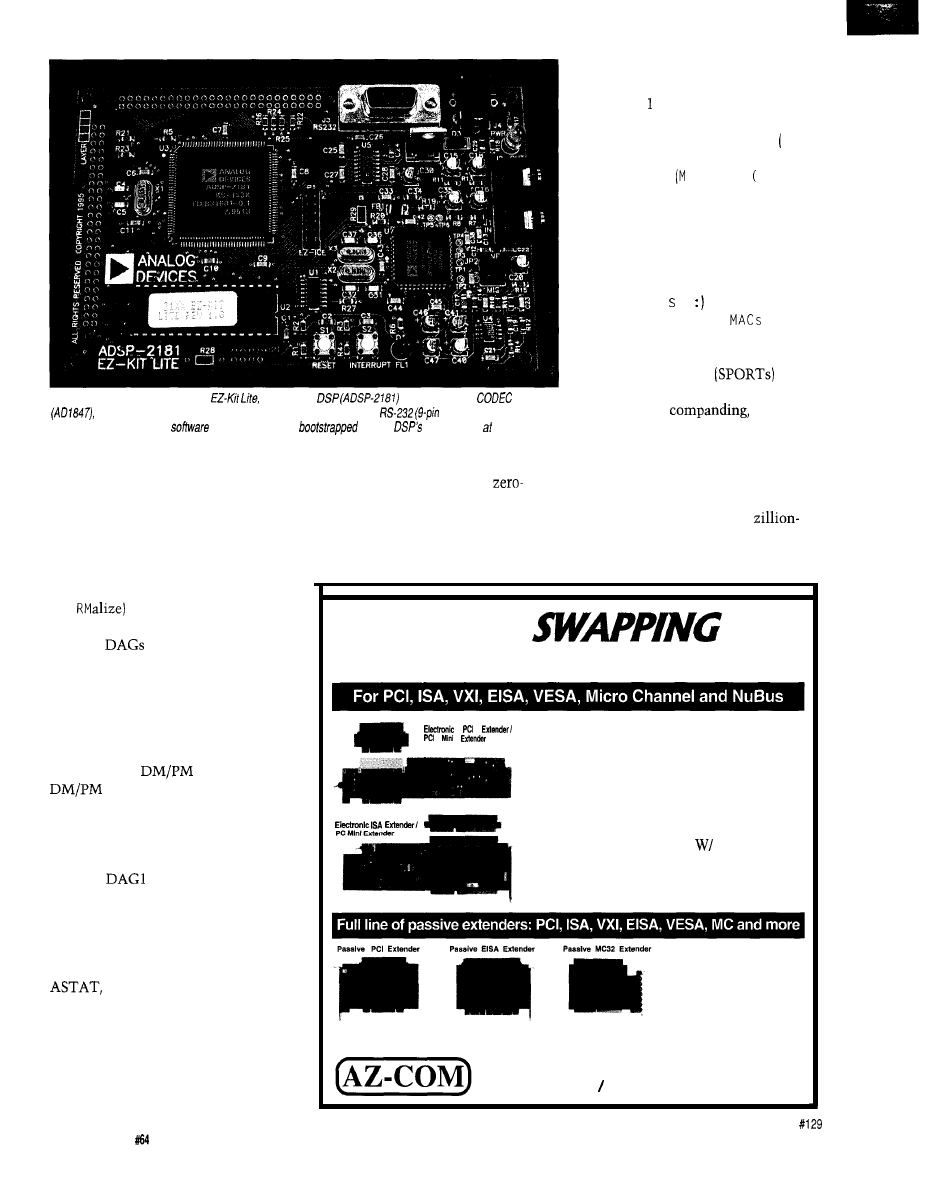
Photo l-Despite its
small size,
the
combining a
and 16-M stereo
is a complete sonic subsystem that communicates with a PC via
connector). The EPROM
contains monitor and demo
that is automatically
info the
on-chip RAM reset.
operation like
MR = MR + (MX
l
MY)
puts the result in MR and sets flags in
MF.
Shifter inputs include an operand
(SI), exponent (SE), and block exponent
(SB). As these registers’ names imply,
besides the usual bit spinning, the
shifter supports operations (such as
N 0
that speed software floating
point.
The
are responsible for
generating the operand addresses and
consist of I (index), M (modify), and L
(length] registers. Naturally, the I reg-
ister holds the operand address with M
automatically added (postmodify) after
each access. A load instruction takes
the form reg =
(In,Mn) where
refers to the data or program
memory, respectively. The L register
supports modulo addressing (i.e., it
defines the length of a circular buffer
and automatically corrects I for wrap-
around).
can also be configured
to automatically generate bit-reversed
addresses, a technique commonly used
in FFT computations.
The program sequencer contains a
variety of status registers including
MSTAT, and SSTAT for the
ALU, MAC, and shifter, respectively.
Notably, most instructions feature
conditional execution based on a sta-
tus (Z, C, V, etc.) flag.
Particularly important for DSP
applications is a dedicated CNTR
typical termination test and condi-
tional branch.
Listing gives you a taste of ‘2181
programming with a loop (DO
1 a be 1
U
NT I L C E),
conditional execution
I F
MV SAT MR),
and program and data
memory addressing
X 0 = DM I 0 ,
Ml)).
With shades of superscalar, you’ll
even notice that the ‘2 18 1 can execute
multiple instructions at once, typically
combining operand load/stores and an
ALU or MAC operation. In this case,
the inner loop
( o
p
loads both oper-
ands (MXO, MYO) and
them in a
single cycle.
The ‘2 18 l’s specific add-ons in-
clude two serial ports
that
work just like the port on the ‘1847
(i.e., timeslots,
etc.), a
high-speed 16-bit timer, and 13 parallel
I/O
lines (two are shared with SPORT
register and specialized stack, which
1
and three are output only).
work together to implement
As shown in Figure 7, from the
overhead looping. Once the count,
outside, the ‘2181 looks more like a
loop, and fall-through addresses are
simple single-chipper than a
initialized, the loop automatically runs
pin RISC. The bus interface consists of
to completion without the need for the
a 24-bit data and 14-bit address bus
HOT
ELECTRONIC EXTENDERS
l
Insert/Remove Cards With PC Power On!
l
Save Time Testing And Developing Cards
l
Save Wear On Your PC From Rebooting
l
Adjustable Overcurrent Sensing Circuitry
l
NO Fuses, All Electronic For Reliability
l
Single Switch Operation
Auto RESET
l
Optional Software Control Of All Features
l
Breadboard Area For Custom Circuitry
1
Year Warranty
and 30 Day
Money Back
Guarantee
Call
our
24
Hour Fax-On-Demand System for FREE Information.
3343
Vincent Road, Suite D, Pleasant Hill, CA 94523
TEL: 800-209-2418 FAX: 510-947-1900
74
Issue November 1995
Circuit Cellar INK@
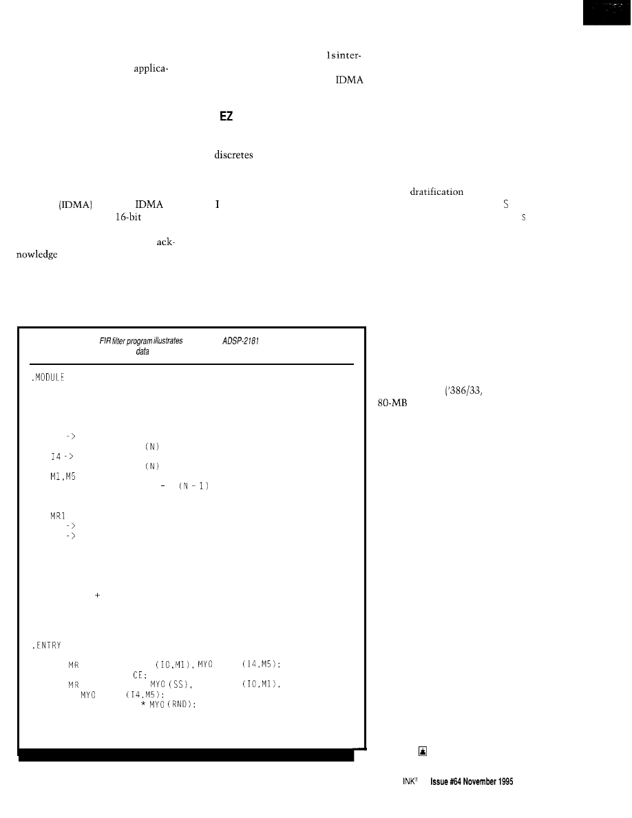
strobed with separate data, program,
access doesn’t need another address
common, I/O, and byte selects.
cycle. In this way, all the ‘218
Recognizing that most
nal RAM (but not control registers) is
tions execute on-chip, the Byte DMA
made directly accessible via the
controller (
BDMA
) reconfigures the
bus by assigning eight of the data lines
as addresses, boosting addressability to
4 MB. In particular, the BDMA solves
the bootstrap problem since it can
automatically load the on-chip RAM
at reset.
Another way to boot and other-
wise talk to the ‘2181 is via the Inter-
nal DMA
port. The
port
consists of a dedicated
multi-
plexed address and data bus with the
requisite read, write, strobe, and
control lines. Access is a
two-step process that sets the address
and then accesses the data.
Note that the address is automati-
cally incremented, so a sequential
port.
THE WAY OUT
You
can see that combining an
ADSP-2181, AD1847, EPROM, and a
few
should be easy. In fact,
the only thing easier is picking up the
phone and ordering the EZ-Kit Lite,
shown in Photo 1.
have to admit I’m a sucker for
cute little demo boards, especially
when they cost less than $100 and do
something useful. The EZ-Kit Lite
easily fills both bills since $89 not
only includes the board, but also com-
plete (not restricted demo versions)
copies of the PC-based assembler,
linker, and simulator.
Listing l--This simple
a number of
programming features
including looping, simultaneous
transfer and computation, and conditional execution.
fir-sub;
FIR transversal filter subroutine
Calling Parameters
IO Oldest input data value in delay line
LO = Filter length
Beginning of filter coefficient table
L4 = Filter length
= 1
CNTR = Filter length 1
Return Values
= Sum of products (rounded and saturated)
IO Oldest input data value in delay line
14 Beginning of filter coefficient table
Altered Registers
MXO, MYO, MR
Computation Time
N 1 + 5 2 cycles
All coeff and data values are assumed to be in 1.15 format.
f i r ;
fir:
= 0, MXO = DM
= PM
DO sop UNTIL
sop:
= MR + MXO *
MXO = DM
= PM
MR = MR + MXO
IF MV SAT MR;
RTS:
.ENDMOD;
Though the tightest loops will
likely remain the province of assembly
language, the DSP world is headed
(like it or not) toward C along with
everyone else. Fortunately, exploiting
the evermore popular GNU C, a com-
plete compiler, library, and debugger
suite only costs $395.
For instant gratification, the board
comes with short-and-sweet demos
(bandpass filter, ADPCM, DTMF,
echo-cancel, etc.). Well, more like
instant
in my case since
shoving the disk in and typing
ETU P
got me a disturbing message:
T h i
program requires Windows to
install.
It’s time to ‘fess up and admit I
don’t have Windows running. I do
most of my office work on a Mac and
have been able to get by, until now,
using DOS for engineering. Sure, I’ve
been planning to upgrade someday, but
figured I’d hold off until about Win-
dows 97.
Wanting to get on with it, I briefly
considered installing Windows 3.1 on
my brand X clone, but a quick glance
under the hood
1 -MB RAM,
hard disk) brought me to my
senses.
Instead, I simply dragged the demo
setup (board, speaker, microphone,
cables, disks, etc.-you know the drill)
over to a Windows-enabled friend’s
house and checked it out there. I can
attest that the demos work as adver-
tised, but didn’t really wring the board
out since we spent most of the time
fiddling with
AUTOEXEC. BAT.
I left my
friend with a cheery “Thanks, bro’,
and don’t forget to uninstall.”
Funny thing is, once you get past
the Windows-Or-Else install proce-
dure, you’ll find that most of the soft-
ware is (ho-ho] DOS stuff anyway!
In fact, some programs (such as the
simulator) only work with plain-old
DOS and won’t run in a Windows
DOS-box.
I don’t mean to get on Analog
Devices’ case, though I wish they’d
made the demo DOS friendly. Instead,
just consider this a cautionary harbin-
ger of things to come as the machina-
tions of a desktop-driven Microsoft
collide with the realities of embedded
systems.
Circuit Cellar
75
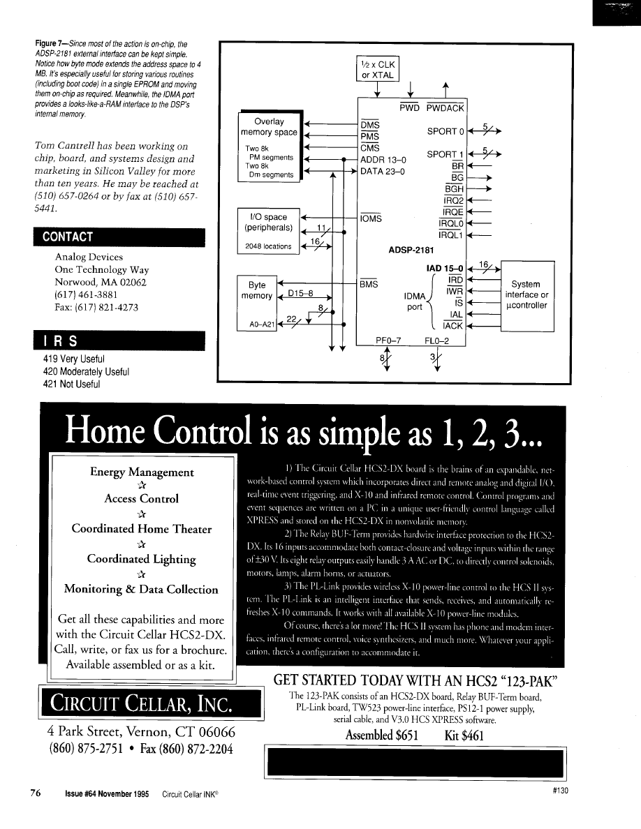

The Circuit Cellar BBS
bps
24 hours/7 days a week
(860) 871-l 988-Four incoming lines
Internet E-mail:
you
haven’t already read my editorial, go check it out if you’re one
of the many who’ve been asking us to put together a Web page.
While if’s far from complete, it’s a
In
month’s BBS threads, we start by looking at an elegant
way of packing more into a limited space without resorting
complicated compression algorithms. In the other discussion, many
people immediately blame equipment failures on heat without taking
info account another likely factor: humidity.
Information Theory
From: Dave Ewen To: All Users
I have what I think is a simple information theory prob-
lem: If I have, say, 37 symbols available (not a power of
and want to transmit a bit stream with them, how could I
map these symbols to make best use of them?
From: Russ Reiss To: Dave Ewen
If all symbols occur with equal likelihood, about all
you can do is use 6 bits to encode the symbols, since it’s the
smallest integer number of bits that can represent your 37
symbols. But, since you mention information theory and
efficiency of transmission, let’s presume that your symbols
don’t occur with equal probability (for example, alphanu-
merics spelling out words in some language).
It can be more efficient in this case to design a code in
which the more-likely-to-occur symbols use shorter code
sequences, whereas less-likely symbols have longer codes.
On the average (simply the weighted sum of the code length
times the probability of occurrence of the symbol, summed
over all symbols), your code could be shorter than the 6-bit
“brute force” code approach.
It’s been said that some of this technique was applied
to Morse Code. For example, the letter E, which has high
probability of occurrence, is encoded as a single dot, where-
as the letter Q, with low probability, is a longer
dot-dash.
Even with numbers thrown in, there are no symbols
longer than five code elements (dots and dashes), except
when you get into punctuation, most of which is six ele-
ments long. In fact, all the letters are four or fewer elements
long. All the numbers are exactly five elements long. But
78
Issue
November 1995
Circuit Cellar INK@
it’s not really a binary code, since the spaces between code
elements are as important as the elements. That’s the only
way letters (symbols) are separated from one another. So,
don’t be too impressed by the seeming efficiency.
You will find techniques for generating the most effi-
cient codes possible based on whatever symbol probability
you have in classical books on information theory.
From: Dave Ewen To: Russ Reiss
Well, it finally dawned on me that the simple solution
was that some symbols would be worth 6 bits and some
bits. But I’m not sure that is the optimum solution; as you
say, frequency of expected usage could be important..
From: Russ Reiss To: Dave Ewen
It’s all up to frequency of occurrence! Consider the
extreme, that one symbol occurred with 99.99% frequency
(I never said it was realistic!). You’d want that symbol to be
coded with a single bit if possible. You really don’t care how
long the codes for other symbols would be. Your average
message length (over a long sequence of symbols) would
come very close to
1
bit per symbol in this case.
Now, I’m not saying this is typical at all (I often use
extreme cases to illuminate a point), but if there is any
reasonable order to the symbol probabilities (i.e., not purely
random], then you can shorten the average message length
by using the right code.
From: Lee
To: Dave Ewen
Another possibility that avoids the use of
length coding would be to use your 64 6-bit numbers to
encode your 37 symbols directly, and use the 27 numbers
left over to encode common symbol combinations. (If we
were encoding English text, some of the single symbols
would be used to encode common words like “the,” and
others might encode common letter combinations.)
From: Dave Ewen To: Russ Reiss
This stuff about probabilities works fine with ASCII
text, but my interest is something similar to
The question I’m pondering now is how I might make use
of unused range. For example if I have a variable that ranges
over integer values O-87, I need 7 bits to encode it, but the
possible values 88-127 are (seemingly) wasted.
From: Russ Reiss To: Dave Ewen
Well, it works with any symbols which do not have
equal probability of occurrence (i.e., completely random].
About the only thing you might do with unused symbols is
what was suggested by another: use them to encode pairs or
triples of symbols, especially those which might occur with
higher probability (if there are any). Even if all equally like-
ly, you’d gain a little this way, and not waste the codes.
From: Robert Lunn To: Dave Ewen
Gee, among all this discussion of probabilities, variable
bitlength hamming codes, and so on, I’m almost afraid to
suggest it. Why don’t you just store your codes as base-40
numbers?
This is an ancient technique that was used for storing
text strings in compilers (error messages, etc.) back when a
minicomputer with 16 KB of memory was a large machine.
A base-40 number obviously lets you encode 40 sym-
bols, which nicely covers the letters A-Z, the digits O-9,
and space, comma, full stop, and
for punctuation.
Now 40 x 40 x 40 = 64,000. So three base-40 numbers
fit neatly into one 16-bit word. Storage is reduced by
and the encode and decode functions are trivial.
From: James Meyer To: Robert Lunn
Three numbers in one 16-bit word, huh? Sixteen bits
divided by three is five and one third bits. If you throw
away the one third bit, you have five bits per word left.
That’s only 32 different characters. If you can provide fur-
ther illustration, I’d be grateful.
From: Robert Lunn To: James Meyer
Of course, Jim. I will even “prove” it.
Consider an alphabet. Indeed, consider the 26-letter
Roman alphabet. Now, I’m thinking of a letter between A
and Z. How can I tell you which one? Clearly, I have to give
you sufficient information to distinguish between 26 differ-
ent possibilities or states.
If the symbols I am using to send information to you
are each capable of this many states, then one symbol will
suffice. If my symbols are more restricted (say, only a dot
and a dash) then I can concatenate symbols to create the
number of states that I need.
Now I want to send you two letters from the Roman
alphabet. How much information must I send?
Assume the first letter is A. It can be followed by any of
A-Z, and so this two pair combination takes 26 states.
Assume the first letter is B. It also can be followed by
any of A-Z, and so this takes *another* 26 states.
You will see that to represent all possible two-letter
combinations drawn from a
alphabet I will need
26 x 26 distinguishable states.
By similar extension you will see that to represent all
possible three-letter combinations drawn from a 26-letter
alphabet I will need 26 x 26 x 26 distinguishable states.
Now let’s expand the alphabet to include more charac-
ters. How about 40 characters? To represent all possible
three-letter combinations drawn from a 40 character alpha-
bet I will need 40 x 40 x 40 distinguishable states.
So to send to you a specific three-letter sequence from
my
alphabet, I must give you sufficient infor-
mation to pick one state from a possible 40 x 40 x 40 =
64,000 states.
A concatenation of sixteen symbols drawn from a
symbol alphabet can represent
= 65,536 states. Such a
concatenation therefore provides more than enough states
for my purpose.
Such a concatenation is conveniently represented in a
computer by 16 binary digits. Thus, a 16-bit word is able to
contain enough information to specify every possible se-
quence of three letters drawn from a
alphabet.
Now let’s show a specific implementation.
I suggested our
alphabet comprise O-9,
A-Z, space, comma, period, and question mark. A conve-
nient coding is:
becomes 37
A-Z becomes 1035
becomes 38
becomes 36
becomes 39
Having coded our characters thus, we can store three
characters, cl, in a
word
(((cl x 40) + c2) x 40) + c3
The number will never exceed 63,999 and so cannot
overflow 16 bits.
Given we can retrieve the three characters:
= mod 40
= div 40) mod 40
cl = div 1600
The singular advantage of this scheme is the simplicity
of encoding and decoding the characters.
Circuit Cellar INK@
Issue
November 1995
From: James Meyer To: Robert Lunn
completely misinterpreted your original message and
was trying to divide the 16-bit word into three pieces on an
integer bit boundary. It’s clear to me now what you were
trying to show me and I’ll never forget it. It’s truly elegant!
Question: I can see that the base-40 scheme works well
for optimizing storage, but how about transmission?
The base-40 method requires that the length of the
message is either fixed and known in advance or is some
multiple of three characters. For example, if I encoded a
message by the base-40 method and had to send it 8 bits at a
time, the receiver would have a hard time with the decod-
ing if he missed the very first 8 bits.
Might that be one reason that many encoding schemes
include a “null” character? I noticed that you didn’t include
one in your example.
From: Robert Lunn To: James Meyer
Well, actually I looked up your posts over the last few
months. From these I could see that your background was
primarily in hardware (yes?) and in that area you obviously
knew what you were doing. Therefore, you were simply
misunderstanding me and it was worth my time to explain.
It is my experience that hardware people tend to have a
more “nuts and bolts” approach to software, and can fail to
see some of the subtleties involved. In the same way, of
course, the many subtleties of solid-state electronics go
right over *my* head.
The coding scheme was originally used (to my knowl-
edge) for storing static character strings back when memory
was much more limited than today. For this purpose it
works OK.
However, it falls way short of “optimizing storage.”
Even as a first approximation you can see that only
64000165536 = 97.7% of the “channel” capacity is used.
Transmission systems use much more complicated
methods (which also address the issues of link establish-
ment, flow control, error detection and correction, etc.)
because the cost of implementing these methods is out-
weighed by the savings in reduced transmission times.
There are no control characters in the example I gave. It
would, of course, be easy to define
as an escape code
Micromint’s
chip is
an upgraded replacement for the
venerable Intel
chip
$19.00
chip. Ours is designed for indus-
trial use and operates over the
100
$12.00
entire industrial temperature
range (-40°C to
Available
in
DIP or PLCC.
BASIC-52
manual
$15.00
MICROMINT, INC. 4 PARK STREET, VERNON, CT 06066
82
Issue
November 1995
Circuit Cellar INK@
or Laptop
M-bit microcontrollers
The
is:
Fast--A
high speed
baud)
multidrop master/slave
network
. Flexible-compatible with your
microcontrollers
Reliable-robust
CRC and
sequence number error checking
Efficient-low microcontroller
Motorola 6llHCl
resource requirements (uses
Process
your chip’s built-in serial port)
Friend/y-
Simple to use C and
assembly language software
libraries, with demonstration
programs
Complete-includes network
Fire
software, network monitor and
Security
RS-485 hardware
distributed
617350.7550

and then interpret the following code as having some addi-
tional meaning.
However, note that all of the 16-bit numbers 64,000
through 65,535 are unused. All of these can be used to im-
plement such flow control functions as <start of block>,
of block>, <acknowledge>, <idle>, and so on.
Of course, the 16-bit words used for such a purpose
cannot then also encode data.
Having reached consensus, I can make the following
points:
You will now see that the statement in my first post
that 40 x 40 x 40 = 64,000 does in fact constitute proof of
my original assertion.
You will also have realized when reading my last mes-
sage that base-40 numbers (or any other type of number] are
themselves simply letters drawn from some alphabet, or,
more generally, simply symbols. Thus the whole exercise is
just a conversion of one set of symbols into another.
Thus the whole argument becomes wonderfully circu-
lar. This is the region where number theory, complexity
theory, information theory, graph theory, and so on all re-
veal themselves to be different ways of looking at the same
thing. Many people claim that this says something pro-
found about the universe..
From: James Meyer To: Robert Lunn
This BBS isn’t called the *Circuit
l
Cellar for nothing.
Yep, although I have done some programming, I’m better at
circuit design.
Perhaps your original claim was proof, but it certainly
wasn’t obvious to this solder-slinger until you showed me
the algorithm, though. An example or two makes it much
easier for me. I guess that’s just the way my mind works.
Running PC in warm environment
From: Lee Leduc To: All Users
I have a question about running a PC clone at a room
temperature of 85°F. Is it safe to operate a PC at this tem-
perature. I’m setting up a BBS and the building has no air
conditioning. In ancient times,
years ago, I had prob-
lems with memory chips running in an ambient tempera-
ture above 90”. The specs I can find on the memory, CPU,
and other chips in the system claim a commercial tempera-
ture range (0-70°C) for these components. I’m using a CPU
fan and a temp. probe placed inside the case of the machine
shows a temperature of
Any opinions would be
welcomed.
From: Ken Simmons To: Lee Leduc
FWIW, I’ve had my system in a 90” environment and it
hasn’t had any problems.
As long as the internal temperature remains below
you should be all right.
Oh, don’t forget to regularly vacuum all the accumu-
lated dust and such from inside your system. If any of the
fan vents in the power supply get clogged, air flow is re-
duced and efficient cooling doesn’t happen.
From: Janice Marinelli To: Ken Simmons
Sometimes humidity is the factor that pushes it over
the top. Like humans, they seem to be able to take more
heat as long as the humidity is not through the roof too.
From: Ken Simmons To: Janice Marinelli
remember a situation where I installed an automated
test system controlled by an H/P 1000 computer and a 7906
cartridge drive. The customer started having disk-access
problems and data errors. I eventually traced the problem to
too much humidity supplied by the room’s air conditioner/
humidifier-the thick air (I think it was
ing) was causing the disk read errors. As soon as the humid-
ity was reduced to a more manageable
the disk errors
went away and never returned!
I sometimes ponder how PCs in “tropical” locales (i.e.,
East Coast in summer) manage to keep functioning with
the high temps and humidities? I’m thankful I live in the
Puget Sound area where the humidity rarely breaks 50%
without condensation.
From: George Novacek To: Ken Simmons
If the computer is running, its internal temperature is
above ambient and, therefore, the relative humidity inside
the box is lower. What you must be wary of is water ingress
due to high humidity, which happens when the machine is
turned off and allowed to cool down to the ambient tem-
perature.
This is one argument for leaving the computer on all
the time (this is too controversial and a completely different
subject). When you run temperature and humidity test
cycles on electronic equipment, it is much more likely to
fail after you have soaked it in a low temperature or high
humidity environment and then powered up, as
opposed to keeping it energized.
Any properly made electronic equipment should take
60% RH indefinitely, especially if we are talking an
conditioned environment. The ambient temperature is
Circuit Cellar INK@
Issue
November 1995
8 3

maintained fairly low and, consequently, the interior of the
equipment will work at significantly lower RH without
exceeding its maximum temperature rating. The compo-
nent aging and stress come primarily from the elevated
temperature. You do not want to operate close to the maxi-
mum rating.
for corrosion, especially on all nongold-plated connections
(e.g., printer and modem cables]. You’d be amazed at what
humidity will do to mere cadmium-plated, nickel-plated,
and chrome-plated surfaces after awhile.
I would be a little apprehensive using a computer built
with parts rated for 50°C max. operating temperature in
Saudi Arabia. But we have had equipment built with 70°C
rated parts running nonstop for years in Singapore, where
humidity gets to 95% or higher without a problem.
From: George Novacek To: Ken Simmons
the air warms up, the internal humidity will rise
the external, just because of the nature of water
From: Ken Simmons To: George Novacek
To a point, of course. If the ambient humidity is rela-
tively high to begin with, the air pulled into the machine
via the fan will also have that humidity. Once the air
warms up, the internal humidity will rise above the exter-
nal, just because of the nature of water vapor.
Quite the opposite. Once the air has warmed up, its
relative humidity drops. This is precisely why you have
static electricity problems in the wintertime. The following
is an excerpt from an encyclopedia:
Having worked in environmental stress-screening for
the past 9 years, I’ve witnesses this phenomenon and..
not pretty sometimes.
the water-vapor content of air, is ex-
pressed as a fraction of the mass of water vapor in a given
mass of air-usually taken as 1 kg (2.2 lb.)-it is called spe-
cific humidity. A variable quantity, it ranges from 0% in
very dry air to as much as 4% in very humid air.
is one argument for leaving the computer on
the time.
True. However, it’s best if you can control the humid-
ity somewhat inside the machine. One way is desiccant
packs, available from packing-supply companies. The 1” x
1” packs are relatively cheap and you can toss a few into
your machine for a month (or so?) of dehumidification.
“The upper limit of the amount of water that air can
hold in vapor form is called the saturation specific humid-
ity. At surface atmospheric pressure (1,000 millibars) the
maximum is 0.1 of water vapor per kilogram of air at a
temperature of -40°C (-40°F); at the freezing point the ratio
is 3.8
at 20°C (68°F) it is 15
and at 40°C
it is 50 g/kg, or 5%.
Any properly made circuit board that expects to operate
on 60% RH *should* be conformal coated to minimize
moisture infiltration, especially if that humidity should
turn condensing. Even more so if the temperature should
suddenly rise (i.e., heat wave).
“Relative humidity (RH) is actual specific humidity
measured as a percent of saturation specific humidity. For
example, if relative humidity is 90% at the freezing point (a
very high value), then specific humidity is 3.4 g/kg. Relative
humidity is the most widely used humidity indicator..
Finally, you need to remember what high ambient
humidity does to humans: it causes them to sweat pro-
fusely and that same sweat drips into places you don’t want
it to go. Add body salt (and other electrolytes) that are
mixed with that sweat and you have the makings of elec-
tronic disaster via unwanted conductive paths, etc. Another
argument for dehumidification or conformal-coating of
electronic gear (especially consumer-oriented gear).
What the above boils down to is that if you had 95%
RH at 68°F ambient and warmed up the air inside the com-
puter to
the RH *would* *drop* from 95% to a
mere 28%. Then, let the equipment cool down and if its
temperature drops below 68°F where the RH hits
or
the saturation point, you’ll get condensation, soaking the
electronics in water.
Otherwise, what you state is quite valid.
have had equipment built with 70°C rated parts
nonstop for years in Singapore, where humidity
to 95% or higher without a problem.
Where I come from, a properly made PCB *is*
ally coated. I’m not familiar with PC manufacturers’ stan-
dards. Again, it’s not the heat wave you should worry about,
but a sudden temperature drop-that is when you get con-
densation (e.g., fog).
like you’ve found winners there in that equipment.
Sounds like you’ve found winners there in that equip-
We did not find the winners, we built them. However,
ment. One caveat, though: you should do periodic checks
if you want to swap stories of what corrosion can do to
84
Issue
November 1995
Circuit Cellar INK@
equipment, count me out. It’s just too depressing. Seeing
equipment after only a couple of days of salt fog test makes
me cry. :-(
From: Ken Simmons To: George Novacek
Given that information, if the starting air doesn’t have
much humidity (absorbed water vapor) to begin with, I have
to agree that warming said low-moisture air, without pro-
viding more moisture to balance it, will result in a humid-
ity decrease. Am I right in concluding that’s what you’re
trying to say here?
However, if you do provide more humidity to that
warmed air, the RH will rise again, regardless of the target
temperature. That’s what I see happening in the PC envi-
ronment with a continuous flow of air into and out of the
machine. There’s always a little bit of stagnant air inside
that’11 tend (as I see it) to absorb any moisture and keep it
there, especially considering the rather poor air flow from
the typical case vent design.
Now, I agree that if you have an initially warm, humid
atmosphere and you cool it, you’ll get condensation/precipi-
tation (a common occurrence here in the Puget Sound area).
However, with the cooling mechanism used for the PC
innards, the temperature differential between interior and
exterior will rarely be more than
Let me explain.
I have a thermometer on my home system monitoring
the PC fan exhaust (I have a ‘286 system). Even when the
ambient temperature is over
the exhaust temperature
rarely breaks
Even the normal exhaust temperature,
with 70-75°F external temperature, only hovers around
85°F.
Additionally, I have what’s called a silencer, which is a
temperature-controlled fan-speed regulator attached to my
PC’s fan. This results in having the cooling fan operating at
half speed (i.e., approx. 6 VDC applied to the
fan),
which not only reduces the noise, it reduces the internal
dust buildup due to a lower flow rate. I’ve had it in my
machine for over 7 years and it rarely (if ever) speeds up due
to over-temperature problems, even in summer.
Now, when you talk about your typical tropical envi-
ronments, where the RH is
for
temperature,
the humidity change will not be that dramatic, if at all,
when that hot, humid air is drawn into the (perhaps) warm-
er PC inside. Furthermore (and I think you’ll agree with me
here), humid air is a poorer heat conductor than dry air
(relatively speaking). Therefore, PC innards in a tropical (or
desert) environment will not be cooled as well as one in a
more temperate environment.
It’s the nature of water vapor, once heated, to resist
further attempts at absorbing more heat as the vapor con-
centration increases. That’s why there’s very little percep-
tual difference between 70% and 90% RH compared to
between 40% and 70% RH. Add dissolved salt to that hu-
mid, tropical air (i.e., coastal environments), and you’ll
agree you have the makings of a very hostile environment
for modern electronics (which you mention later).
I come from, a properly made PCB *is* conformally
I’m not familiar with PC manufacturers’ standards.
True. If you look at PC motherboards, they do have a
very minimal coating that, to my observation at least, ap-
pears to be nothing more than the solder mask. The chips
and sockets are bare to the environment, so they’re gonna
get the brunt of punishment.
As to the cooling factor, that’11 happen when you turn
it off, regardless of the ambient environment. It is that pow-
er cycling which, I think you’ll agree, is what causes the
damage to occur with corrosion.
Where I work (Boeing Military), our
are encapsu-
lated with either silicone or urethane resin (Hysol, PC-18M)
so they can handle salt-fog, dust, and humidity without
failing.
I used to clean equipment that had been through
fog qualification testing. Aside from crusting, our stuff
washed clean (with lots of warm, deionized water, that is!)
and operated to
after being fogged and summarily
cleaned.
And I second your grief regarding corrosion damage on
consumer- and industrial-grade stuff. All the military-grade
stuff I’ve worked on seemed to be relatively immune from
any type of corrosion.
From: Pellervo Kaskinen To: Ken Simmons
However, if you do provide more humidity to that
air, the RH will rise again, regardless of the target
That’s what I see happening in the PC.
I fail to see it happening that way at all! True, *if
l
you
introduce more moisture, the RH of course starts increas-
ing, but where does that additional moisture come from?
Surely you are not suggesting there are some famous
Demons, selectively kicking each water molecule from the
dryer air into the more humid pocket you advocate.
The only pockets approaching such behavior are found
where pressurized air expands and cools, not when the tem-
perature is increasing, with pockets or not.
The reason why you might see more failures when the
humidity increases is not related to the temperature in-
creasing locally. It is due to the higher relative humidity in
the general atmosphere, which means that even after the
Circuit Cellar
November 1995
8 5
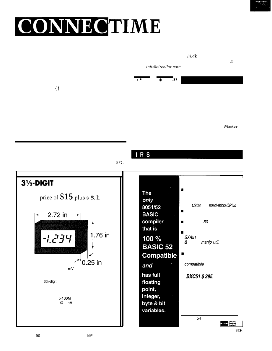
RH is reduced by heating, it is not reduced to as low a value
as it would be when the ambient RH is lower.
What the higher temperature does in addition to the
higher RH is promote the migration of water through the
polymeric materials, such as plastic packages of the semi-
conductors. Once the water reaches the chip, all kinds of
problems may arise. (Yes, Jim, I know the chips have a pro-
tective passive layer
Corrosion of the very thin bonding
wires is just one of the things.
Now, although we have been talking about increased
RH causing problems to electronics, the opposite is much
more true in my books. The low RH gives rise to some
pesky static discharge damages. I may not have seen the
high humidity as a real problem in the equipment we build,
but I sure have seen the dead chips due to static electricity
every year after the beginning of the heating season.
We invite you to call the Circuit Cellar BBS and exchange
messages and files with other Circuit Cellar readers. It is
available 24 hours a day and may be reached at (860)
1988. Set your modem for 8 data bits, 1 stop bit, no parity,
and 300, 1200, 2400, 9600, or
bps. For information on
obtaining article software through the Internet, send
mail to
Software for the articles in this and past issues of
Circuit Cellar INK
may be downloaded from the Circuit
Cellar BBS free of charge. For those unable to download
files, the software is also available on one 360 KB IBM
PC-format disk for only $12.
To order Software on Disk, send check or money
order to: Circuit Cellar INK, Software On Disk, P.O.
Box 772, Vernon, CT 06066, or use your Visa or
Card and call (860) 8752199. Be sure to specify the issue
number of each disk you order. Please add $3 for
shipping outside the U.S.
422 Very Useful
423 Moderately Useful
424 Not Useful
LCD PANEL METER
-Available now at an unheard of
N e w ! N o t s u r p l u s !
Specifications:
Maximum input: k199.9
additional ranges provided through
external resistor dividers
Display:
LCD, 0.5 in. figure height,
jumper-selectable decimal point
Conversion: Dual slope conversion, 2-3
readings per sec.
Input Impedance:
ohm
Power: 9-12 VDC 1
DC
Circuit Cellar, Inc.
4
Park Street, Suite 12, Vernon, CT 06066
Tel: (860) 875-2751
Fax: (860) 872-2204
86
issue
November 1995
Circuit Cellar
n
Memory mapped variables
In-line assembly language
option
n
Compile time switch to select
805
1 or
Compatible with any RAM
or ROM memory mapping
Runs up to
times faster than
the MCS BASIC-52 interpreter.
Includes Binary Technology’s
cross-assembler
hex file
n
Extensive documentation
Tutorial included
q
Runs on IBM-PC/XT or
q
Compatible with all 8051 variants
n
508-369-9556
FAX 508-369-9549
q
Binary Technology, Inc.
P.O. Box
l
Carlisle, MA 01741

They Still
he Circuit Cellar
had a great time at the Embedded Systems Conference in San Jose. Not only
was there no question about Circuit Cellar’s dominant niche in the publishing market, embedded-control
manufacturers have come to truly recognize the caliber and excellence of our readers. By the end of the show, we
had spoken with all the major embedded-system players, committed to some really neat projects for next year, and
scheduled a couple of ambitious industry-sponsored design contests.
As you might expect, everyone leaves this kind of convention thinking that every discipline is ultimately a candidate for
embedded control. Implementation is just a matter of timing and price.
To physically test this concept, stopped at the Restaurant Equipment Manufacturer’s convention in Las Vegas before returning.
Given all the compufunctions,
bells and whistles jammed into the average consumer toaster, I figured they’d probably stuffed a
into a
commercial dishwasher by now. I expected you could measure water temperature,
dissolved solids,
viscosity, soap-film density, residue reflective indices, motor currents, sprinkler volume, droplet velocity, and on and on. Surely even
washing a dish would now be a whole new experience.
about an undiscovered country. The kitchen side of the food industry must have “If it ain’t broke, don’t fix it!” chiseled
on their butcher block. With the exception of a few OSHA-mandated safety interlocks, today’s dishwasher and practically everything
else in the restaurant is the same as what I used during high school.
Unless the computer controls are so embedded that they’re invisible, saw very little in the way of mechanical-control replacement
or innovative new features requiring microcontroller technology. The $20,000 gas ovens use piezoelectric mechanical starters
and bimetallic temperature regulators. Refrigerators? Well, they’re still plain old refrigerators. No built-in bar-code inventory systems yet.
Except for a couple of electronic temperature-probe manufacturers ardently searching for customers, there was a phenomenal
lack of sophistication in food-preparation equipment. The one light on the horizon, brightly shining with a plethora of formula and
concoction alternatives, was the abundance of automatic cappuccino and espresso machines. The literature from Acorto proudly
describes how its powerful microprocessor monitors and controls all the major functions to produce one of any 26 drinks “at the touch
of a button.”
While not completely discouraged, it was obvious that my search for automatic electronic hamburger flippers was useless.
In fact, I wondered if there wasn’t even a bit of regression going on.
In one booth, I smelled hamburgers cooking. The tray of samples attracted my attention that much more. I listened to the sales
pitch about it being the fastest hamburger cooker available and how by using “direct energy transfer,” it could cook two burgers in 25
seconds with no flipping. To everyone else, “direct energy transfer” was obviously something wonderful and worth every penny. To an
electrical engineer, it was a provocation: “Say what?”
The salesman didn’t really want to explain direct energy transfer. After all, a heating element under a pan transfers heat to the
food, doesn’t it? The key word is “direct.” Take a couple %-lb. chunks of ground beef, squash them between two stainless steel
electrodes, apply
watts of energy for 25 seconds, and I’d say you could call that direct energy transfer! In nonfood-speak, it’s
still electrocuted beef.
Deep under the covers, suspect a micro modulates the current to keep the burger from becoming a charcoal briquette, but the
salesman didn’t know. The ultimate shocker wasn’t the technique, but the price. At $1900, I decided to cook hamburgers the
fashioned way with catsup and with or without embedded control.
A
So much for introducing new technology to restaurant kitchens.
96
Issue
November
1995
Circuit Cellar
Wyszukiwarka
Podobne podstrony:
circuit cellar1996 11
circuit cellar1993 11
circuit cellar1994 11
circuit cellar1997 11
circuit cellar2004 11
circuit cellar2000 11
circuit cellar2002 11
circuit cellar2001 11
circuit cellar2003 11
circuit cellar1996 11
circuit cellar1993 11
circuit cellar1995 11
circuit cellar1996 11
circuit cellar2003 11
circuit cellar1997 11
circuit cellar1993 11
więcej podobnych podstron