
F2833x - PWM and Capture Units
7 - 1
Introduction
Today’s electronic systems are described using terms such as “direct digital control”, “digital
power supply”, “digital power converters” and so on. A core feature of all these applications is
the ability to generate different series of digital pulse patterns to control power electronic
switches based on the results of sophisticated numerical calculations. The F283xx family
provides such hardware units; several pulse width modulation (PWM) output signals, along with
time measurements units (“Capture Units”).
In Chapter 6 we have already implemented a time base unit, using the CPU core timers 0 to 2.
Although these units are also hardware based time units, they are only able to 'signal' the end of a
pre-defined period. On such an event, an interrupt service routine could be requested to start and
perform desired activities by a software sequence. While this scenario is sufficient for most time-
based software activities, it is not suitable for hardware related actions, such as switching the
control line of an output stage from passive to active. In this case we need much more precise and
automatic response to the actuator control lines, based on different events on the timeline. This is
where PWM - lines come into the play.
The main applications of PWM are:
• Digital Motor Control (DMC)
• Control of switching pulses for Digital Power Supply (DPS) systems
• Analogue Voltage Generators
Later we will discuss these main application areas in more detail. The F2833x is equipped with
different and independent numbers of PWM channels; a F28335, for example, has 6 PWMs.
The F2833x is also able to perform time measurements using hardware signals. With the help of
independent edge detector state machines, called ‘Capture Units’ we can measure the time
difference between edges to determine the speed of a rotating shaft in revolutions per minute or
the active duty cycle of a feedback signal.
A third hardware part of the Control System is called a ‘Quadrature Encoder Pulse’ -unit (QEP).
This is a unit that is used to derive the speed and direction information of a rotating shaft directly
from hardware signals from incremental encoders or resolvers.
Our lab series Lab 7-1 to Lab 7-9 will include the most important operating modes of a PWM
signal. A typical requirement in control loop calculations is the operation using complex
numbers, which are translated according to Euler's law into sine and cosine components. Instead
of calculating a new sine-value each time we need one, we can access a look-up table, which is
already available inside the F283xx! This is exactly what we will do in Lab 7- 9 (“Generate a
pulse width modulated sine wave signal”) to implement a practical example.
F2833x PWM, Capture and QEP

Module Topics
7 - 2
F2833x - PWM and Capture Units
Module Topics
F2833x PWM, Capture and QEP ..............................................................................................................7-1
Introduction .............................................................................................................................................7-1
Module Topics ..........................................................................................................................................7-2
ePWM Block Diagram .............................................................................................................................7-3
ePWM Time Base Unit .............................................................................................................................7-4
ePWM Phase Synchronisation .................................................................................................................7-5
Timer Operating Modes ...........................................................................................................................7-6
Time Base Registers .................................................................................................................................7-7
Lab 7_1: Generate an ePWM signal ......................................................................................................7-11
Lab 7_2: Generate a 3 - phase signal system ........................................................................................7-16
Purpose of Pulse Width Modulation ......................................................................................................7-19
ePWM Compare Unit .............................................................................................................................7-21
ePWM Action Qualification Unit ...........................................................................................................7-24
Lab 7_3: A 1 kHz signal with variable pulse width ...............................................................................7-30
Lab 7_4: a pair of complementary 1 kHz-Signals ..................................................................................7-32
Lab 7_5: Independent Modulation on ePWM1A / 1B ............................................................................7-34
ePWM Dead Band Module ....................................................................................................................7-38
Lab 7_6: Dead Band Unit on ePWM1A / 1B .........................................................................................7-43
ePWM Chopper Module ........................................................................................................................7-46
Lab 7_7: Chopped Signals at ePWM1A / 1B .........................................................................................7-50
ePWM Over Current Protection ............................................................................................................7-52
Lab 7_8: Trip Zone protection with TZ6................................................................................................7-56
ePWM Interrupt Sources ........................................................................................................................7-61
Lab7_9: ePWM Sine Wave Modulation .................................................................................................7-65
eCAP Capture Module ...........................................................................................................................7-71
Capture Units Registers .........................................................................................................................7-74
Lab7_10: ePWM1A 1 kHz signal captured by eCAP1 ...........................................................................7-79
Enhanced QEP module ..........................................................................................................................7-82
Infrared Remote Control ........................................................................................................................7-84
Lab7_11: eCAP4 to receive a RC5 IR-signal ........................................................................................7-87
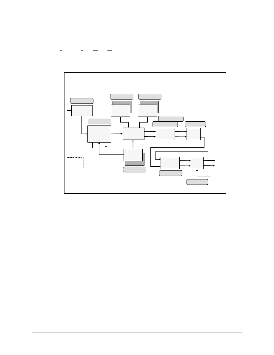
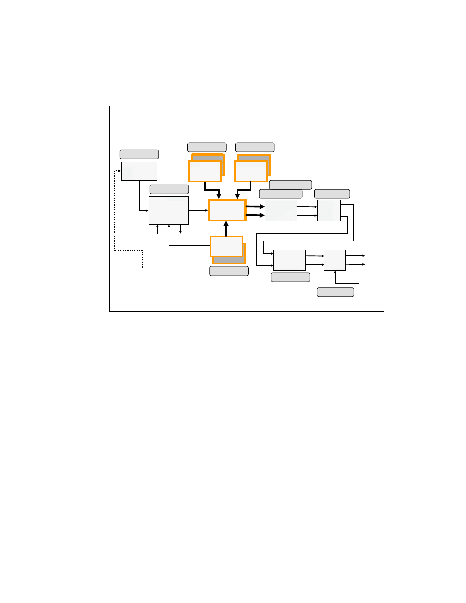
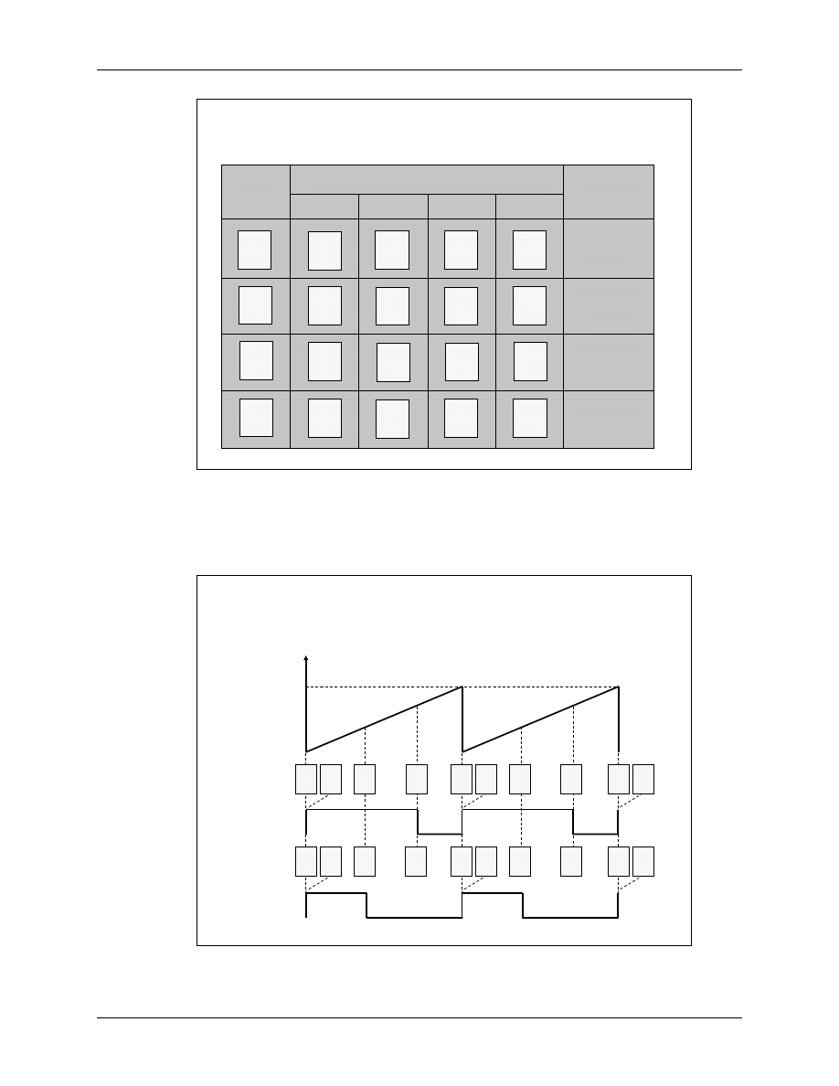
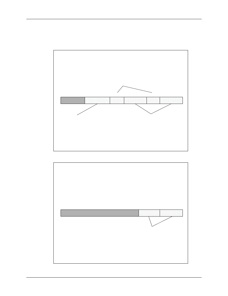
ePWM Block Diagram
F2833x - PWM and Capture Units
7 - 3
ePWM Block Diagram
Each enhanced Pulse Width Modulation (ePWM) unit is controlled by its own logic block, as
shown in Slide 7_2 below. This logic is able both to automatically generate signals on different
time events and also to request various interrupt services from the F2833x PIE interrupt system,
to support its operational modes.
7
7
-
-
2
2
ePWM Block Diagram
ePWM Block Diagram
16
16
-
-
Bit
Bit
Time
Time
-
-
Base
Base
Counter
Counter
Compare
Compare
Logic
Logic
Action
Action
Qualifier
Qualifier
Dead
Dead
Band
Band
PWM
PWM
Chopper
Chopper
Trip
Trip
Zone
Zone
Shadowed
Compare
Compare
Register
Register
Shadowed
Period
Period
Register
Register
Clock
Clock
Prescaler
Prescaler
Shadowed
Compare
Compare
Register
Register
CMPA . 15 - 0
CMPB . 15 - 0
TBCTR . 15 - 0
TBPRD . 15 - 0
TBCTL . 12 - 7
AQCTLB . 11 - 0
AQCTLA . 11 - 0
DBCTL . 4 - 0
PCCTL . 10 - 0
TZSEL . 15 - 0
EPWMxA
EPWMxA
EPWMxB
EPWMxB
SYSCLKOUT
SYSCLKOUT
TZy
TZy
EPWMxSYNCI
EPWMxSYNCI
EPWMxSYNCO
EPWMxSYNCO
TBCLK
TBCLK
A unique feature of an ePWM - module is its ability to start the Analogue to Digital Converter
(ADC) without software interaction, directly from an internal hardware event. A common
microcontroller would have to request an interrupt service to do the same - the F2833x does this
automatically. We will use this feature in the next module!
Note: There are two basic operating modes of the ePWM system: (1) standard ePWM 16-bit
mode and (2) 24-bit High Resolution PWM mode (HRPWM). For now we will discuss the 16-bit
mode.
The purpose of an ePWM unit is to generate a single ended signal or a pair of output signals,
called EPWMxA and EPWMxB, which are related to each other. The lower case letter x is a
placeholder for the number of the ePWM unit, e.g. 1…6.
Note: to generate a physical output signal on the F2833x we have to set the multiplex registers for
the I/O ports accordingly - please refer to Chapter 5!
As you can see from Slide 7-2, to generate a physical output signal we will have to setup a few
units: time base, compare logic, action qualifier, dead band unit, chopper and trip zone. On first
glance this looks cumbersome. However, it does allow us to setup a range of different operating
modes, all of which can be used in modern digital control. So, let us make use of it!
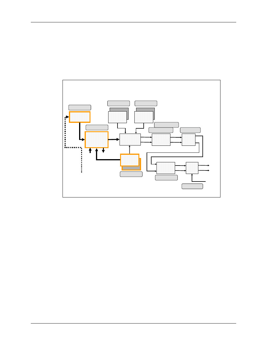
ePWM Time Base Unit
7 - 4
F2833x - PWM and Capture Units
ePWM Time Base Unit
The central block of an ePWM unit is a 16-bit timer (register "TBCTR"), with signal
SYSCLKOUT as its time-base. In Chapter 5 we initialized the core to run at 100 MHz or 150
MHz, depending on the external clock of the F2833x. This frequency sets the time-base for all
ePWM units.
7
7
-
-
3
3
ePWM Time
ePWM Time
-
-
Base Module
Base Module
16
16
-
-
Bit
Bit
Time
Time
-
-
Base
Base
Counter
Counter
Compare
Compare
Logic
Logic
Action
Action
Qualifier
Qualifier
Dead
Dead
Band
Band
PWM
PWM
Chopper
Chopper
Shadowed
Compare
Compare
Register
Register
Shadowed
Period
Period
Register
Register
Clock
Clock
Prescaler
Prescaler
Shadowed
Compare
Compare
Register
Register
CMPA . 15 - 0
CMPB . 15 - 0
TBCTR . 15 - 0
TBPRD . 15 - 0
TBCTL . 12 - 7
AQCTLB . 11 - 0
AQCTLA . 11 - 0
DBCTL . 4 - 0
PCCTL . 10 - 0
SYSCLKOUT
SYSCLKOUT
EPWMxSYNCI
EPWMxSYNCI
EPWMxSYNCO
EPWMxSYNCO
TBCLK
TBCLK
Trip
Trip
Zone
Zone
TZSEL . 15 - 0
EPWMxA
EPWMxA
EPWMxB
EPWMxB
TZy
TZy
A clock prescaler (register TBCTL, bits 12 to 7) can be used to reduce the input counting
frequency by a selectable factor between 1 and 1792.
Register TBPRD defines the length of a period of an output signal, in multiples of the time-period
of the input signal.
Another unique feature of the F2833x is its “shadow” functionality of operating registers, in the
case of ePWM units available for compare register A, B and period register. For some
applications it is necessary to modify the values inside a compare or period register, every period.
The advantage of the background registers is that we can prepare the values for the next period in
the current one. Without a background function we would have to wait for the end of the current
period, and then trigger a high prioritized interrupt. Sometimes this form of scheduling will miss
its deadline…
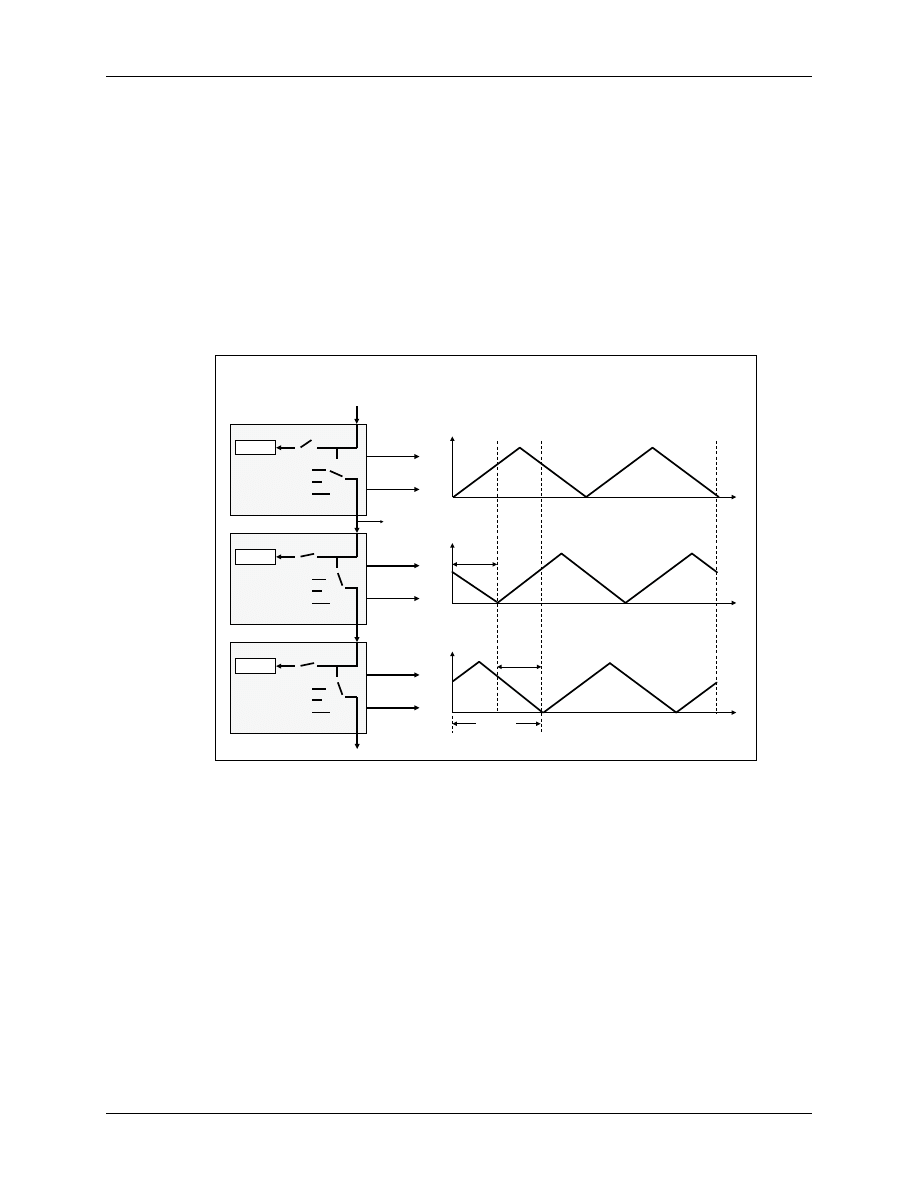
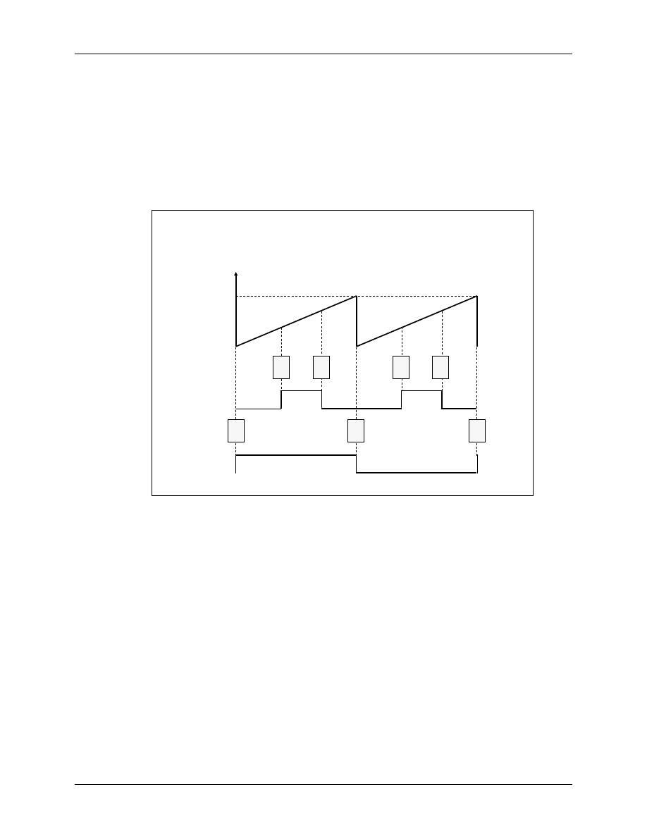
ePWM Phase Synchronisation
F2833x - PWM and Capture Units
7 - 5
ePWM Phase Synchronisation
Two hardware signals "SYNCI" (synch in) and "SYNCO" (synch out) can be used to synchronize
ePWM units to each other. For example, we could define one ePWM unit as a "master" to
generate an output signal "SYNCO" each time the counter equals period. Two more ePWM units
could be initialized to recognize this signal as "SYNCI" and start immediately counting, each
time they receive this signal. In such way we have established a synchronous set of 3 ePWM
channels. But we can do even better. By using another register called "TBPHS" we can introduce
a phase shift between master, slave 1 and slave 2, an absolute necessity for three-phase control
systems.
7
7
-
-
4
4
ePWM Phase Synchronization
ePWM Phase Synchronization
SyncIn
SyncIn
SyncOut
SyncOut
CTR=zero
CTR=zero
CTR=CMPB
CTR=CMPB
X
X
En
En
o
o
o
o
o
o
o
φ
φ
=120
=120
°
°
Phase
Phase
.
EPWM2A
EPWM2A
EPWM2B
EPWM2B
SyncIn
SyncIn
SyncOut
SyncOut
CTR=zero
CTR=zero
CTR=CMPB
CTR=CMPB
X
X
En
En
o
o
o
o
o
o
o
φ
φ
=240
=240
°
°
Phase
Phase
.
EPWM3A
EPWM3A
EPWM3B
EPWM3B
SyncIn
SyncIn
SyncOut
SyncOut
CTR=zero
CTR=zero
CTR=CMPB
CTR=CMPB
X
X
En
En
o
o
o
o
o
o
o
φ
φ
=0
=0
°
°
Phase
Phase
.
EPWM1A
EPWM1A
EPWM1B
EPWM1B
φ
φ
=120
=120
°
°
φ
φ
=120
=120
°
°
φ
φ
=240
=240
°
°
Ext. SyncIn
(optional)
To eCAP1
SyncIn
Slide 7-4 shows such an example, where register TBCNT of ePWM2 and ePWM3 are preloaded
with a start value that corresponds to 120° and 240° respectively. In this example ePWM1 has
been initialized as master to generate SYNCO each time the counter register equals zero. With the
enabled phase input feature for ePWM2 and ePWM3 the two channels operate as slave 1 and
slave 2 and will load their counter registers TBCNT with numbers stored in the corresponding
phase registers TBPHS.
Example:
•
ePWM1 counts from 0 to 6000. TBPRD = 6000
•
ePWM2 register TBPHS = 2000
•
ePWM3 register TBPHS = 4000
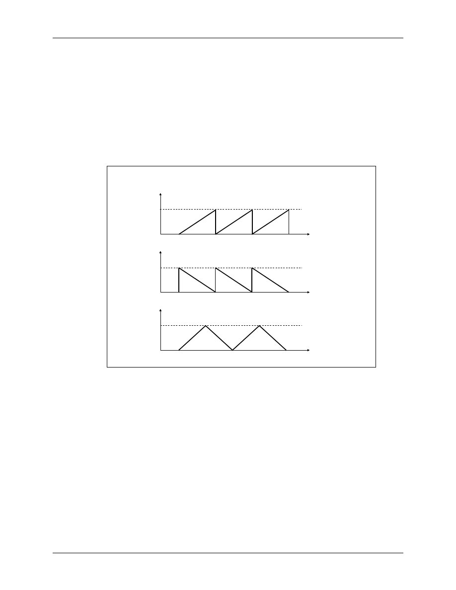
Timer Operating Modes
7 - 6
F2833x - PWM and Capture Units
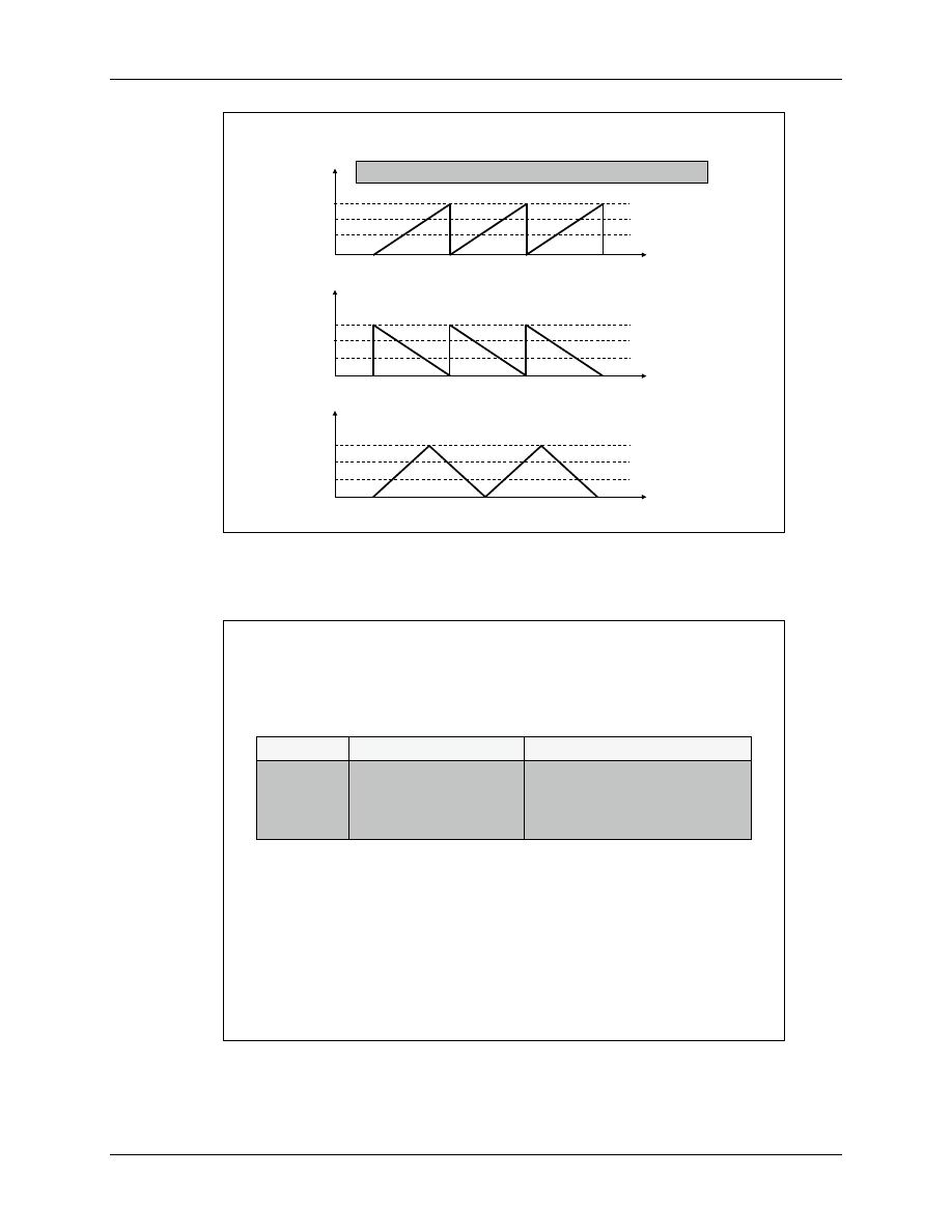
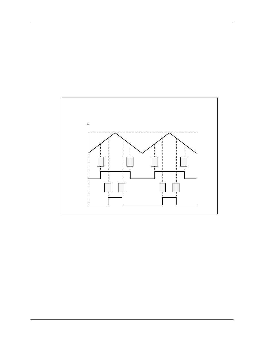
Timer Operating Modes
Each ePWM module is able to operate in one of 3 different counting modes, selected by bits 1
and 0 of register TBCTL:
•
count up mode
•
count down mode
•
count up and down mode
7
7
-
-
5
5
ePWM Time
ePWM Time
-
-
Base Count Modes
Base Count Modes
TBCTR
TBCTR
TBCTR
TBCTR
TBCTR
TBCTR
TBPRD
TBPRD
TBPRD
TBPRD
TBPRD
TBPRD
Count Up Mode
Count Up Mode
Count Down Mode
Count Down Mode
Count Up and Down Mode
Count Up and Down Mode
Asymmetrical
Asymmetrical
Waveform
Waveform
Asymmetrical
Asymmetrical
Waveform
Waveform
Symmetrical
Symmetrical
Waveform
Waveform
Which of the three modes is used is mostly determined by the application. The first two operating
modes are called "Asymmetrical" because in of the shape of the counting pattern from 0 to
TBPRD (count up) or from TBPRD to 0 (count down). Also, in a three phase system, one could
define three different timing events between 0 and TBPRD to switch a phase output signal to
"ON" and to use the match between TBCNT and TBPRD to switch "OFF" all three phases
simultaneously, thus generating an asymmetrical shape of the switch signals.
In "Symmetrical" waveform mode, the register TBCNT starts from zero to count up until it equals
TBPRD. Then TBCNT turns direction to count down back to zero to finish a counting period.
Time Base Registers
F2833x - PWM and Capture Units
7 - 7
Time Base Registers
To initialize the time base for one of the ePWM units it is necessary to initialize a first group of
registers, shown in slide 7-6:
7
7
-
-
6
6
ePWM Time
ePWM Time
-
-
Base Module Registers
Base Module Registers
Name
Name
Description
Description
Structure
Structure
TBCTL
TBCTL
Time
Time
-
-
Base Control
Base Control
EPwm
EPwmx
Regs.TBCTL.all
Regs.TBCTL.all
=
=
TBSTS
TBSTS
Time
Time
-
-
Base Status
Base Status
EPwm
EPwmx
Regs.TBSTS.all
Regs.TBSTS.all
=
=
TBPHS
TBPHS
Time
Time
-
-
Base Phase
Base Phase
EPwm
EPwmx
Regs.TBPHS
Regs.TBPHS
=
=
TBCTR
TBCTR
Time
Time
-
-
Base Counter
Base Counter
EPwm
EPwmx
Regs.TBCTR
Regs.TBCTR
=
=
TBPRD
TBPRD
Time
Time
-
-
Base Period
Base Period
EPwm
EPwmx
Regs.TBPRD
Regs.TBPRD
=
=
To access these registers using the C programming language, we can take advantage of the source
code file "DSP2833x_GlobalVariableDefs.c", which defines all memory mapped hardware
registers as global variables. All variables are based on structure and union data types, also
already defined by Texas Instruments and included with a master header file
"DSP2833x_headers.h".
For the purpose of ePWMs this file defines 6 structures "EPwm1Regs" to "EPwm6Regs", which
include all registers that belong to one of these hardware units.
Time related registers such as the period register can be accessed directly, e.g. to define a period
of 6000 count pulses we can use:
EPwm1Regs.TBPRD = 6000;
For control registers, such as TBCTL, the structure members have been defined as unions. This
technique allows us to access the register en bloc (union member "all") or just individual bit
groups (union member "bit"). For example, a line to write the full register TBCTL would look
like this:
EPwm1Regs.TBCTL.all = 0x1234;
A bit field access to fields "CLKDIV" only would look like:
EPwm1Regs.TBCTL.bit.CLKDIV = 7;

Time Base Registers
7 - 8
F2833x - PWM and Capture Units
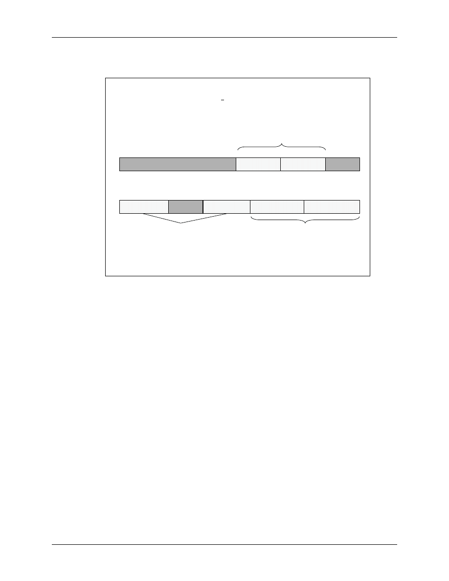
Time Base Control Register TBCTL
The master control register for an ePWM unit is register TBCTL.
7
7
-
-
7
7
ePWM Register TBCTL
ePWM Register TBCTL
Upper Register:
Upper Register:
FREE_SOFT
FREE_SOFT
PHSDIR
PHSDIR
CLKDIV
CLKDIV
HSPCLKDIV
HSPCLKDIV
15
15
-
-
14
14
13
13
12
12
-
-
10
10
9
9
-
-
7
7
TBCLK = SYSCLKOUT / (HSPCLKDIV * CLKDIV)
TBCLK = SYSCLKOUT / (HSPCLKDIV * CLKDIV)
TB Clock
TB Clock
Prescale
Prescale
000 =
000 =
/1 (default)
/1 (default)
001 = /2
001 = /2
010 = /4
010 = /4
011 = /8
011 = /8
100 = /16
100 = /16
101 = /32
101 = /32
110 = /64
110 = /64
111 = /128
111 = /128
High Speed TB
High Speed TB
Clock
Clock
Prescale
Prescale
000 =
000 =
/1
/1
001 = /2 (default)
001 = /2 (default)
010 = /4
010 = /4
011 = /6
011 = /6
100 = /8
100 = /8
101 = /10
101 = /10
110 = /12
110 = /12
111 = /14
111 = /14
Emulation Halt Behavior
Emulation Halt Behavior
00 = stop after next CTR inc/
00 = stop after next CTR inc/
dec
dec
01 = stop when:
01 = stop when:
Up Mode; CTR = PRD
Up Mode; CTR = PRD
Down Mode; CTR = 0
Down Mode; CTR = 0
Up/Down Mode; CTR = 0
Up/Down Mode; CTR = 0
1x = free run (do not stop)
1x = free run (do not stop)
Phase Direction
Phase Direction
0 = count down after sync
0 = count down after sync
1 = count up after sync
1 = count up after sync
(HSPCLKDIV is for legacy compatibility)
FREE_SOFT:
•
controls the interaction between the DSC and the JTAG - Emulator.
•
if the execution sequence of the code hits a breakpoint, we can specify what should
happen with to this ePWM unit.
PHSDIR:
•
specifies if this ePWM unit starts counting up or down after a SYNCIN pulse has
been seen.
•
In case of a single ePWM setup with a disabled sync in feature, this bit is a "don't
care"
CLKDIV and HSPCLKDIV:
•
Prescaler Bit fields to reduce the input frequency "SYSCLKOUT"
•
For a 100MHz-System each pulse translates into 10 ns, for a 150MHz - System into
6.667 ns.
Time Base Registers
F2833x - PWM and Capture Units
7 - 9
7
7
-
-
8
8
ePWM Register TBCTL
ePWM Register TBCTL
Lower Register:
Lower Register:
CTRMODE
CTRMODE
SWFSYNC
SWFSYNC
SYNCOSEL
SYNCOSEL
PRDLD
PRDLD
PHSEN
PHSEN
6
6
5
5
-
-
4
4
3
3
1
1
-
-
0
0
2
2
Software Force Sync Pulse
Software Force Sync Pulse
0 = no action
0 = no action
1 = force one
1 = force one
-
-
time sync
time sync
Sync Output Select
Sync Output Select
(source of EPWMxSYNC0 signal)
00 =
00 =
EPWMxSYNCI
EPWMxSYNCI
01 = CTR = 0
01 = CTR = 0
10 = CTR = CMPB
10 = CTR = CMPB
11 = disable
11 = disable
SyncOut
SyncOut
Counter Mode
Counter Mode
00 = count up
00 = count up
01 = count down
01 = count down
10 = count up and down
10 = count up and down
11 = stop
11 = stop
–
–
freeze (default)
freeze (default)
Period Shadow Load
Period Shadow Load
0 = load on CTR = 0
0 = load on CTR = 0
1 = load immediately
1 = load immediately
Phase Reg. Enable
Phase Reg. Enable
0 = disable
0 = disable
1 = CTR = TBPHS on
1 = CTR = TBPHS on
EPWMxSYNCI
EPWMxSYNCI
signal
signal
SWFSYNC:
•
An instruction that sets this bit will immediately produce a "SYNCO" pulse from this
ePWM unit
SYNCOSEL:
•
Selection of the source for the SYNCO signal.
•
If no channel synchronization is used, switch off this feature
PRDLD:
•
Enables (0) or disables (1) the shadow register function of TBPRD. If disabled, all
write instructions to TBPRD will directly change the period register. If enabled, a
write instruction will store a new value in shadow. With the next event CTR = 0 the
shadow value will be loaded into TBPRD automatically.
PHSEN:
•
Enables (1) the preload of register TBCTR from TBPHS by a "SYNCIN" trigger
CTRMODE:
•
Defines the operating mode of this ePWM unit
Time Base Status Register TBSTS
This register flags the current status of the ePWM unit
Time Base Registers
7 - 10
F2833x - PWM and Capture Units
7
7
-
-
9
9
ePWM Register TBSTS
ePWM Register TBSTS
CTRDIR
CTRDIR
CTRMAX
CTRMAX
SYNCI
SYNCI
reserved
15
15
-
-
3
3
0
0
2
2
1
1
Counter Max Latched
Counter Max Latched
0 = max value not reached
0 = max value not reached
1 = CTR = 0xFFFF (write 1 to clear)
1 = CTR = 0xFFFF (write 1 to clear)
External Input Sync Latched
External Input Sync Latched
0 = no sync event occurred
0 = no sync event occurred
1 = sync has occurred (write 1 to clear)
1 = sync has occurred (write 1 to clear)
Counter Direction
Counter Direction
0 = CTR counting down
0 = CTR counting down
1 = CTR counting up
1 = CTR counting up
CTRDIR:
•
Indicates, if ePWM counts up (1) or down(0)
SYNCI:
•
If an SYNCI event has been seen by this ePWM unit, this bit is 1, if not, it is 0.
•
Note: To clear this bit, one must write a 1 into it!
CTRMAX:
•
If for some reason the 16-bit counter register TBCTR overflows, bit "CTRMAX"
will be set to 1. Under normal circumstances this should not happen, so we can treat
this bit as a security alert signal.
•
Note: To clear this bit, one must write a 1 into it!

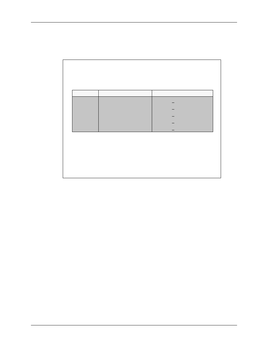
Lab 7_1: Generate an ePWM signal
F2833x - PWM and Capture Units
7 - 11
Lab 7_1: Generate an ePWM signal
Although we have not discussed all the remaining modules inside the ePWM units, let us
start an exercise to generate a single ended ePWM output signal. We will resume the
discussion of additional modules in an ePWM unit later. The following procedure will
guide you through the task of the exercise and will give you all necessary information.
7
7
-
-
10
10
Lab 7_1: Generate a 1 KHz Signal at ePWM1A
Lab 7_1: Generate a 1 KHz Signal at ePWM1A
• Generate a 1 KHz square wave signal at ePWM1A with a
duty cycle of 50 %
• Measure it with an oscilloscope or
• Connect the signal to an external buzzer or loudspeaker
• Registers involved:
• TBPRD:
define signal frequency
• TBCTL:
setup operating mode and time prescale
• AQCTLA:
define signal shape for ePWM1A
Objective:
Objective:
HSPCLKDIV
CLKDIV
T
T
TBPRD
SYSCLKOUT
PWM
∗
∗
∗
=
2
1
Objective
The objective of this lab is to generate a square wave signal of 1 kHz at line ePWM1A.
With the help of an oscilloscope connected to header J6-1 of the Peripheral Explorer
Board, we can monitor the signal. A small external circuit featuring a buzzer would allow
us to make the signal audible. A possible schematic is given at the end of this exercise.
Procedure
Create a new Project File
1.
Using Code Composer Studio, create a new project, called
Lab7.pjt
in
C:\DSP2833x\Labs (or in another path that is accessible by you; ask your teacher or a
technician for an appropriate location!).
2.
Open the file Lab6.c from C:\DSP2833x\Labs\Lab6 and save it as Lab7_1.c in
C:\DSP2833x\Labs\Lab7.
3.
Add this source code file to your new project:
•
Lab7_1.c

Lab 7_1: Generate an ePWM signal
7 - 12
F2833x - PWM and Capture Units
4.
From C:\tidcs\c28\dsp2833x\v131\DSP2833x_headers\source add:
•
DSP2833x_GlobalVariableDefs.c
5.
From C:\tidcs\c28\dsp2833x\v131\DSP2833x_common\source add:
•
DSP2833x_CodeStartBranch.asm
6.
From C:\tidcs\c28\dsp2833x\v131\DSP2833x_common\cmd add:
•
28335_RAM_lnk.cmd
7.
From C:\tidcs\c28\dsp2833x\v131\DSP2833x_headers\cmd add:
• DSP2833x_Headers_nonBIOS.cmd
8.
From C:\CCStudio_v3.3\c2000\cgtools\lib add:
• rts2800_fpu32.lib
9. From C:\tidcs\c28\dsp2833x\v131\DSP2833x_common\source add:
•
DSP2833x_SysCtrl.c
•
DSP2833x_CpuTimers.c
•
DSP2833x_PieCtrl.c
•
DSP2833x_PieVect.c
•
DSP2833x_DefaultIsr.c
•
DSP2833x_ADC_cal.asm
•
DSP2833x_usDelay.asm
Project Build Options
10. We also have to set up the search path of the C-Compiler for include files. Click:
Project
Build Options
Select the Compiler tab. In the "Preprocessor" category, find the Include Search Path (-i) box
and enter the following two lines in this box:
C:\tidcs\C28\dsp2833x\v131\DSP2833x_headers\include;
C: tidcs\C28\dsp2833x\v131\DSP2833x_common\include
11. Set up the floating point support of the C - compiler. Inside Build Options select the Compiler
tab. In the "Advanced" category set "Floating Point Support" to
fpu32
12. Set up the stack size: Inside Build Options select the Linker tab and enter in the Stack Size (-
stack) box:
400

Lab 7_1: Generate an ePWM signal
F2833x - PWM and Capture Units
7 - 13
Close the Build Options Menu by Clicking <OK>.
Build, Load and Test
13. The new project should now behave exactly as it did in Lab6. So far it is nothing more than a
framework to develop our ePWM1A example. Let us test the functionality of this outline
project. Once more, here are the steps:
Project
Build
File
Load Program
Debug
Reset CPU
Debug
Restart
Debug
Go main.
Debug
Run
If the code does not work as it did in Lab6, do not continue with the next steps! Go back and
try to find out which step of the procedure you missed.
Modify Source Code
14. In function "Gpio_select()", set multiplex register line GPIO0 to enable ePWM1A as output
signal.
15. In “main()”, just after the call to the function "Gpio_select()", call a new function "Se-
tup_ePWM1A()". Also, add a new function prototype at the beginning of “Lab7_1.c”:
void Setup_ePWM1A(void);
16. At the end of Lab7_1.c, add the new function "Setup_ePWM1A()". We will use this function
to initialize ePWM1 to generate a 1 kHz square wave signal. We need to setup the following
register:
•
EPwm1Regs.TBCTL
•
EPwm1Regs.TBPRD
•
EPwm1Regs.AQCTLA
To setup the registers we can use either the "all"-member of the register union or the individ-
ual bit field member "bit". An instruction to "all" would require us to calculate a hexadecimal
number for all 16 bits. By using the "bit" - structure we can leave the task to calculate the cor-
rect logical and/or -instruction to set or clear individual bit fields with the C-compiler. As an
example, an instruction to setup the operating mode to "up/down"-mode would look like this:
•
EPwm1Regs.TBCTL.bit.CTRMODE = 2;
Next, we have to calculate the value for register TBPRD. If we use "up/down" - counting
mode, the formula is:
Lab 7_1: Generate an ePWM signal
7 - 14
F2833x - PWM and Capture Units
HSPCLKDIV
CLKDIV
f
f
TBPRD
PWM
SYSCLKOUT
∗
∗
∗
=
2
1
The factor 1/2 must be used in "up/down operating mode. Remember that TBPRD is a 16-bit
register, therefore the maximum number for TBPRD is (2
16
-1) or 65535.
Now, recall the objective is to generate a PWM signal of 1 kHz with the F28335ControlCard
running at 150 MHz. Your task is to calculate appropriate numbers for CLKDIV,
HSPCLKDIV and TBPRD.
In function "Setup_ePWM1A()" initialize:
EPwm1Regs.TBCTL.bit.CLKDIV =
?
EPwm1Regs.TBCTL.bit.HSPCLKDIV = ?
EPwm1Regs.TBCTL.bit.CTRMODE = 2; // up-down mode
EPwm1Regs.TBPRD =
?
EPwm1Regs.AQCTLA.all = 0x0006;
// zero = set; period = clear
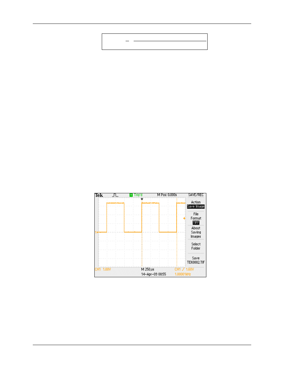
Re-Build, Load and Test
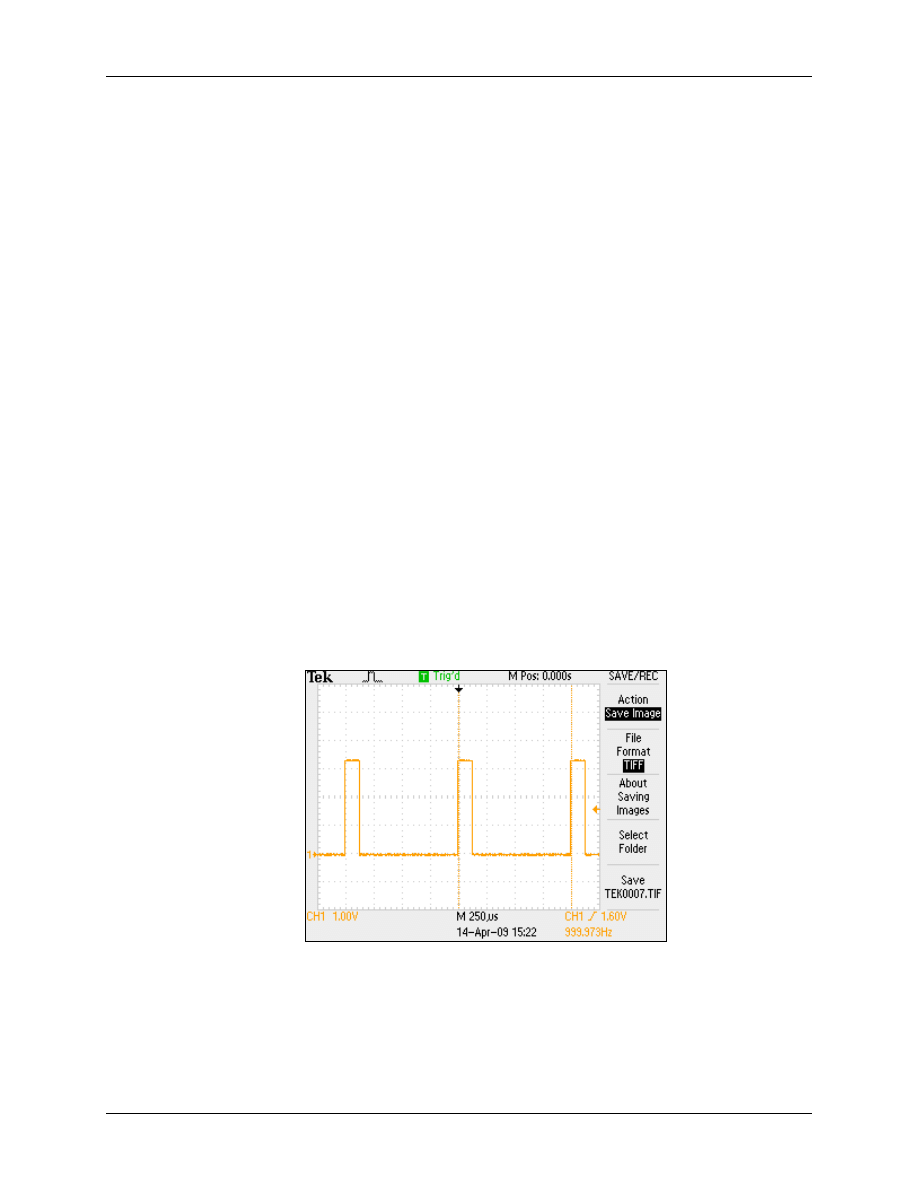
17. Now rebuild, load and test the new project. The program should still show the binary counter
from Lab6 at LEDs LD1 and LD2. The new addition is a 1 kHz - signal at output ePWM1A
(header J6-1 at the Peripheral Explorer Board).
18. Use a scope to inspect this signal. It should look like:
19. Optional exercise: experiment with different frequencies by changing the value for register
TBPRD!
20. Optional Hardware: Make your frequency audible! By adding the following circuitry to your
Peripheral Explorer Board, we can do it!
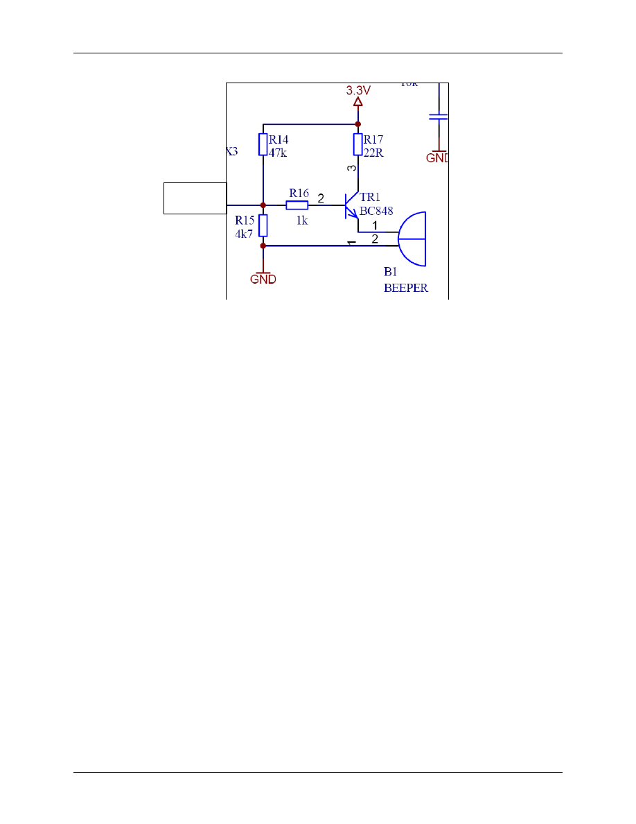
Lab 7_1: Generate an ePWM signal
F2833x - PWM and Capture Units
7 - 15
Device B1 (“Beeper”) can be a Digisound F/SMD8585JSLF (Mouser Part # 847 - FSMD8585JS)
or a Digisound F/PCW04A.
END of LAB 7_1
ePWM1A

Lab 7_2: Generate a 3 - phase signal system
7 - 16
F2833x - PWM and Capture Units
Lab 7_2: Generate a 3 - phase signal system
Now let us experiment with a 3-phase system with a phase shift of 120° and 240°
between the signals. We will use ePWM1A, ePWM2A and ePWM3A for this
exercise. Signal ePWM1A will be the master phase and ePWM2A and 3A will
trail at 120° and 240° respectively.
7
7
-
-
11
11
Lab 7_2: Generate a 3 phase system
Lab 7_2: Generate a 3 phase system
• Generate three 1 KHz square wave signals at ePWM1A, 2A
and 3A with duty cycles of 50 % and a phase shift of 120°
and 240° between the signals
• Measure all three signals with an oscilloscope
• Registers involved:
• TBPRD:
define signal frequency
• TBCTL:
setup operating mode and time prescale
• AQCTLA:
define signal shape for ePWM1A
• TBPHS:
definition of the phase shift for 2A and 3A
Objective:
Objective:
HSPCLKDIV
CLKDIV
T
T
TBPRD
SYSCLKOUT
PWM
∗
∗
∗
=
2
1
Objective
The objective of this lab is to generate a set of 3 square wave signals of 1 kHz each at lines
ePWM1A, ePWM2A and ePWM3A. With the help of a 4 channel oscilloscope connected to
header J6-1, 2 and 3 of the Peripheral Explorer Board, we can visualize the signal.
Procedure
Open Project File
1. If not still open from Lab7_1, re-open project
Lab7.pjt.
2. Open file “Lab7_1.c” and save it as “Lab7_2.c”
3. Remove file “Lab7_1.c” from project and add “Lab7_2.c” to it. Note: optionally you
can also keep “Lab7_1.c” but exclude it from build. Use a right mouse click on file
“Lab7_1.c”, select “File Specific Options”; in category “General” enable “Exclude
from Build”.
Lab 7_2: Generate a 3 - phase signal system
F2833x - PWM and Capture Units
7 - 17
Modify Source Code
4. In file “Lab7_2.c” change the function name “Setup_ePWM1A”. Since we will also
initialize ePWM2A and ePWM3A with this function, the function name is now
somewhat misleading. Change the name into “Setup_ePWM”, including the function
prototype and the calling line in the “main()” - loop.
5. In local function “Gpio_select()”, add instructions to initialize the pin functions of
GPIO2 and GPIO4 to ePWM2A and ePWM3A respectively.
6. In function “Setup_ePWM()”, repeat the initialization for ePWM1A with the same
instructions for ePWM2A and ePWM3A. Apply identical values now to the
following registers:
• EPwm2Regs.TBCTL
• EPwm2Regs.TBPRD
• EPwm2Regs.AQCTLA
• EPwm3Regs.TBCTL
• EPwm3Regs.TBPRD
• EPwm3Regs.AQCTLA
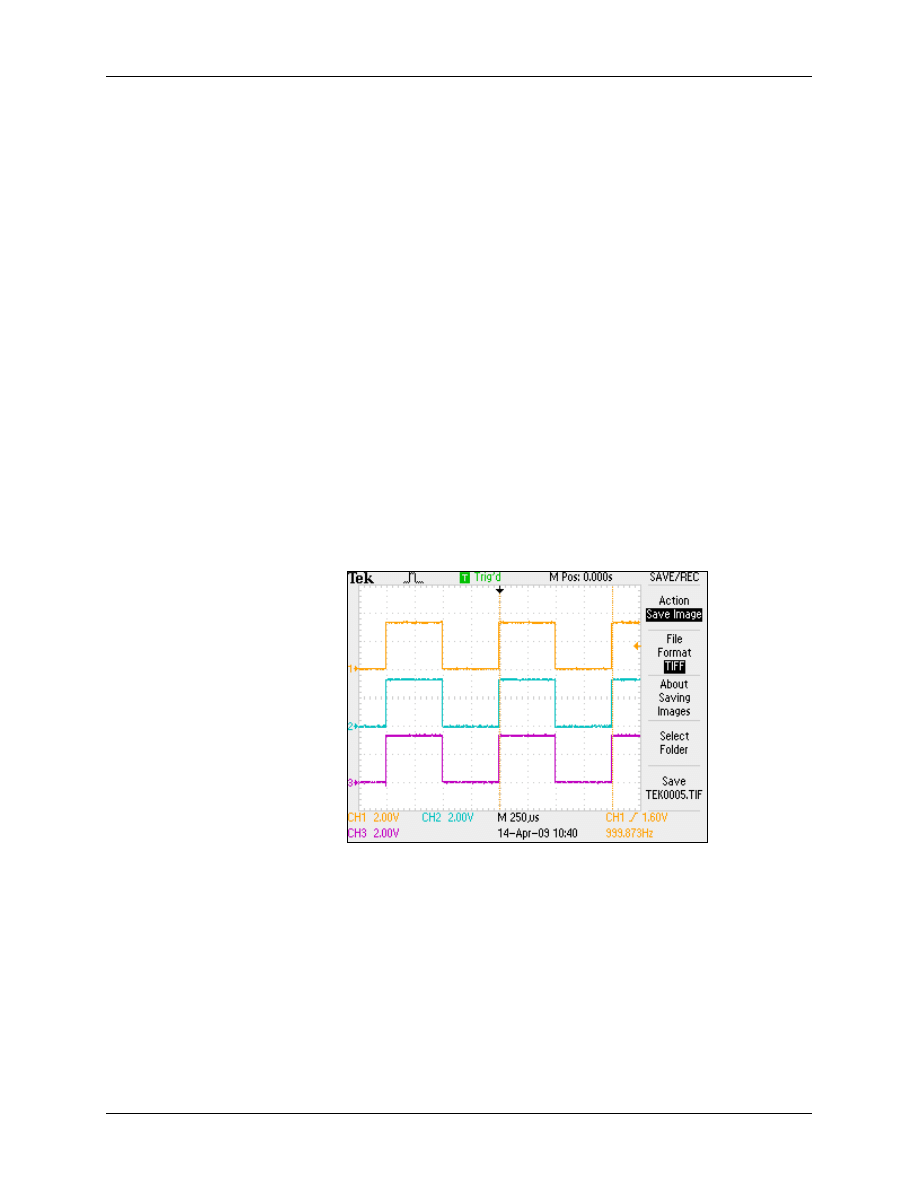
If you now recompile, load and test your new code, you should get 3 identical 1 kHz
- signals with zero phase-shift between the 3 ePWM lines:
7. Now let us add the phase shift commands between ePWM1A, ePWM2A and
ePWM3A. To do so, we will have to program the phase registers of ePWM2A and
ePWM3A. Also, we must define ePWM1A as the master phase to generate a
SYNCOUT pulse each time its counter register TBCNT equals zero. For ePWM2, we
must enable a SYNCIN - pulse and also define SYNCIN as SYNCOUT to drive it
into ePWM3 unit. Recall that the period register TBPRD of ePWM1A has been
initialized with a value that corresponds to a time period of 1 millisecond. Now for
ePWM2 and ePWM3 we need a phase shift of 1/3
rd
and 2/3
rd
of that value preloaded
in register TBPHS.
Summary: In function “Setup_ePWM()” add the following instructions:
Lab 7_2: Generate a 3 - phase signal system
7 - 18
F2833x - PWM and Capture Units
EPwm1Regs.TBCTL:
• Sync Out Select: generate a signal if CTR = 0
EPwm2Regs.TBCTL:
• Set phase enable
• Sync Out Select: SYNCIN = SYNCOUT
EPwm2Regs.TBPHS:
• Load it with 1/3
rd
of TBPRD
• Since TBPHS is a union type, a valid access is made like this:
EPwm2Regs.TBPHS.half.TBPHS = ????? ;
Epwm3Regs.TBCTL:
• Set phase enable
EPwm3Regs.TBPHS:
• Load it with 2/3
rd
of TBPRD
Build, Load and Test
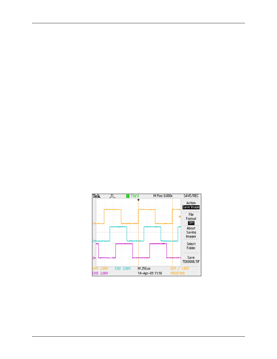
8. Now build, load and test the modified project. Using an oscilloscope you should see 3 time
shifted signals on ePWM1A, ePWM2A and ePWM3A:
END OF LAB 7_2

Purpose of Pulse Width Modulation
F2833x - PWM and Capture Units
7 - 19
Purpose of Pulse Width Modulation
In Lab7_1 and Lab7_2 we created square wave signals with a pulse duty cycle of 50% low and
50% high. We are also able to produce a sequence of time-shifted signals on a group of output
signals. But so far, we are still not able to change or to “modulate” the width of the pulses - even
though this hardware unit is called “Pulse Width Modulation”. This modulation is based on
another set of control registers of a unit called “Compare Module”.
Before we discuss the compare module, let us look into the technical background and purpose of
PWM.
7
7
-
-
12
12
What is Pulse Width Modulation?
What is Pulse Width Modulation?
PWM is a scheme to represent a
PWM is a scheme to represent a
signal as a sequence of pulses
signal as a sequence of pulses
fixed carrier frequency
fixed carrier frequency
fixed pulse amplitude
fixed pulse amplitude
pulse width proportional to
pulse width proportional to
instantaneous signal amplitude
instantaneous signal amplitude
PWM energy
PWM energy
≈
≈
original signal energy
original signal energy
t
Original Signal
Original Signal
T
t
PWM representation
PWM representation
PWM is nothing more than a digital output signal with binary amplitude, 0 or 1. In technical
terms, the voltage at this output pin is either 0V or 3.3V. However, we can setup a point within a
period, at which we switch the output from 0 to 3.3V and vice versa. By changing this set-point
between 0 and 100% of the period, we can adjust the duty cycle of the output signal.
With a PWM signal we can represent any analogue output signal as a series of digital pulses! All
we need to do with this pulse series is to integrate it (with a simple low pass filter) to imitate the
desired signal. This way we can build a sine wave shaped output signal. The more pulses we use
for one period of the desired signal, the more precisely we can imitate it. We speak very often of
two different frequencies, the PWM-frequency (or sometimes “carrier frequency”) and the
desired signal frequency.
A lot of practical applications have an internal integrator. For example the windings of an
electrical motor are perfectly suited to behave as a low-pass filter.
Purpose of Pulse Width Modulation
7 - 20
F2833x - PWM and Capture Units
7
7
-
-
13
13
Why use PWM with Power Switching
Why use PWM with Power Switching
Devices?
Devices?
Desired output currents or voltages are known
Desired output currents or voltages are known
Power switching devices are transistors
Power switching devices are transistors
Difficult to control in proportional region
Difficult to control in proportional region
Easy to control in saturated region
Easy to control in saturated region
PWM is a digital signal
PWM is a digital signal
easy for DSP to output
easy for DSP to output
PWM approx.
PWM approx.
of desired
of desired
signal
signal
DC Supply
DC Supply
Desired
Desired
signal to
signal to
system
system
?
?
DC Supply
DC Supply
Unknown Gate Signal
Unknown Gate Signal
Gate Signal Known with PWM
Gate Signal Known with PWM
PWM
PWM
One of the most used applications of PWM is (A) Digital Motor Control (DMC) and (B) Digital
Power Supply (DPS) - sometimes also called “Switched Power Supply”.
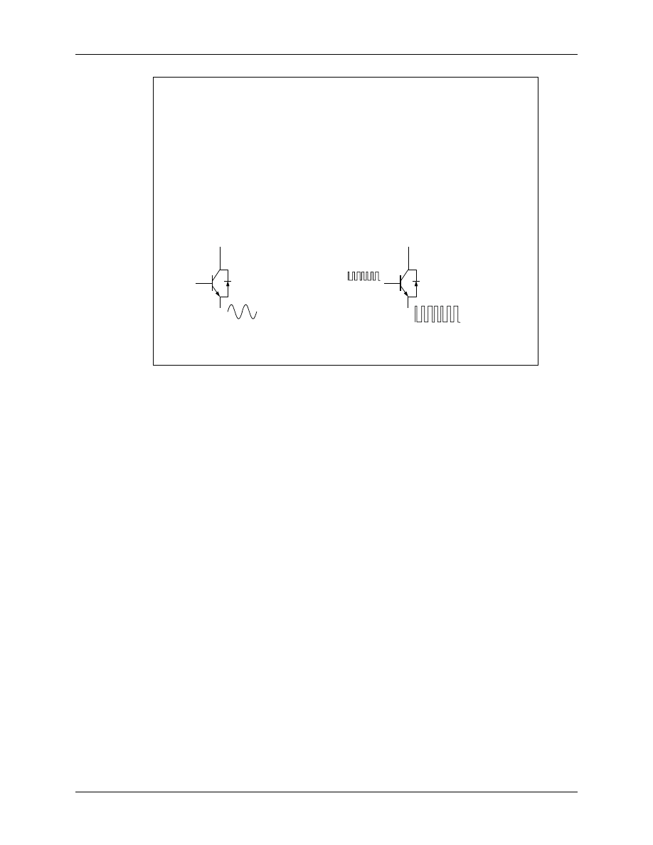
Why is that? Answer: The overall goal is to control electrical drives by inducing harmonic
voltages and currents into the windings of the motor. This is done to avoid electromagnetic
distortions of the environment and to achieve a high power factor. To induce a sine wave shaped
signal into the windings of a motor we would have to use an amplifier to achieve high currents.
The simplest amplifier is a standard NPN or PNP transistor that proportionally amplifies the base
current into the collector current. The problem is, for high currents we cannot force the transistor
into its linear region; this would generate a lot of thermal losses and likely to exceed its maximum
power dissipation.
The solution is to use this transistor in its static switch states only (On: I
ce
= I
cesat
, Off: I
ce
= 0). In
these states, a transistor has its minimum power dissipation. AND: by adapting the switch pattern
of a PWM (recall: amplitude is 1 or 0 only) we can induce a sine wave shaped current!
Environmentally friendly power supply units use switching technologies to increase the
efficiency factor of traditional power supply units. Instead of converting a lot of primary energy
just in pure thermal energy, these techniques, known as “Buck”- or “Boost” - converters, allow
customers to build reduce the package of their goods and more important to help save our
environment.
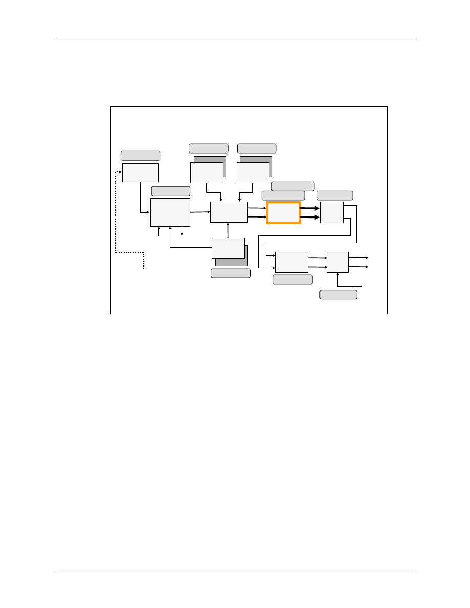
ePWM Compare Unit
F2833x - PWM and Capture Units
7 - 21
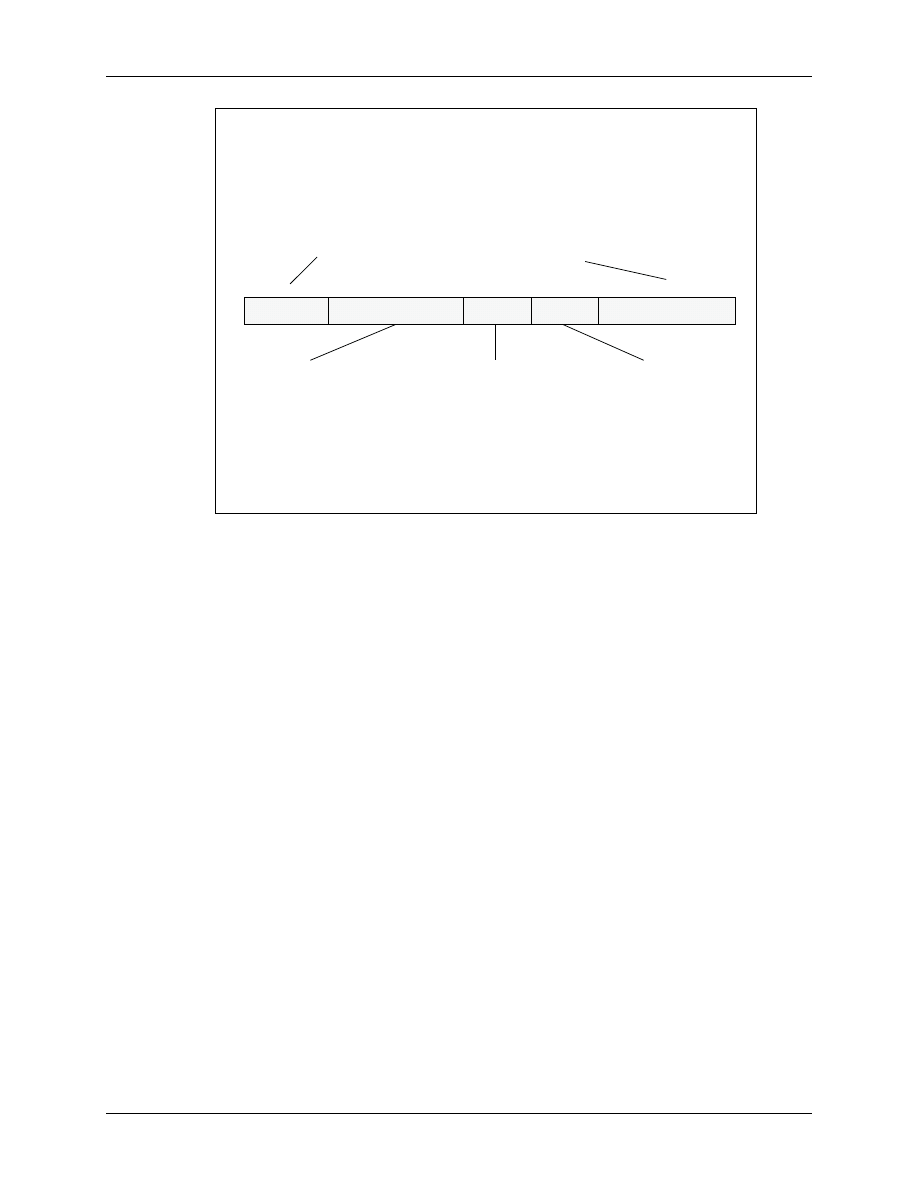
ePWM Compare Unit
The module to control the active phase of a pulse pattern and the position of the switching points
in a PWM is called the “Compare Unit”, highlighted in the next slide:
7
7
-
-
14
14
ePWM Compare Module
ePWM Compare Module
16
16
-
-
Bit
Bit
Time
Time
-
-
Base
Base
Counter
Counter
Compare
Compare
Logic
Logic
Action
Action
Qualifier
Qualifier
Dead
Dead
Band
Band
PWM
PWM
Chopper
Chopper
Shadowed
Compare
Compare
Register
Register
Shadowed
Period
Period
Register
Register
Clock
Clock
Prescaler
Prescaler
Shadowed
Compare
Compare
Register
Register
CMPA . 15 - 0
CMPB . 15 - 0
TBCTR . 15 - 0
TBPRD . 15 - 0
TBCTL . 12 - 7
AQCTLB . 11 - 0
AQCTLA . 11 - 0
DBCTL . 4 - 0
PCCTL . 10 - 0
SYSCLKOUT
SYSCLKOUT
EPWMxSYNCI
EPWMxSYNCI
EPWMxSYNCI
EPWMxSYNCI
TBCLK
TBCLK
Trip
Trip
Zone
Zone
TZSEL . 15 - 0
EPWMxA
EPWMxA
EPWMxB
EPWMxB
TZy
TZy
Its functionality is based on a pair of registers, called “Compare Register A and B” (CMPA and
CMPB). Note that there is no relationship between the letters A and B in these registers and the
naming of the two output signals in the lower right corner, EPWMxA and EPWMxB. This
naming convention is a little bit misleading, it would have been better to use different names such
as CMP1 and CMP2, but the decision was made by Texas Instruments.
Depending on the pre-selected operating mode of the ePWM unit, it is possible to define 2 or 4
events within a period of the PWM - frequency, by choosing the appropriate values in CMPA
and/or CMPB.
Have you kept in mind these operating modes? If not, please review Slide 7-5. Here is a
summary:
• count up mode
• count down mode
• count up and down mode
In Lab7_1 and Lab7_2 we used the up/down mode to generate the 1 kHz signal. We have used
two events to change the voltage level on the output line:
• counter register is zero (TBCNT = 0)
• counter register is equal to period register (TBCNT = TBPRD)
Now we can use 2 or 4 more events:
ePWM Compare Unit
7 - 22
F2833x - PWM and Capture Units
7
7
-
-
15
15
ePWM Compare Event Waveforms
ePWM Compare Event Waveforms
TBCTR
TBCTR
TBCTR
TBCTR
TBCTR
TBCTR
TBPRD
TBPRD
TBPRD
TBPRD
TBPRD
TBPRD
Count Up Mode
Count Up Mode
Count Down Mode
Count Down Mode
Count Up and Down Mode
Count Up and Down Mode
Asymmetrical
Asymmetrical
Waveform
Waveform
Asymmetrical
Asymmetrical
Waveform
Waveform
Symmetrical
Symmetrical
Waveform
Waveform
CMPA
CMPA
CMPA
CMPA
CMPA
CMPA
CMPB
CMPB
CMPB
CMPB
CMPB
CMPB
.
.
.
.
.
.
.
.
.
.
.
.
.
.
.
.
.
.
.
.
.
.
.
.
.
.
.
.
.
.
.
.
.
.
.
.
.
.
.
.
.
.
= compare events are fed to the Action Qualifier Module
= compare events are fed to the Action Qualifier Module
Instead of using 0 or TBPRD we now can use up to 4 more points per period to trigger an action.
What action? Well, the type of action will be defined in another module, coming next. For now
let us summarize the Compare Unit registers:
7
7
-
-
16
16
ePWM Compare Module Registers
ePWM Compare Module Registers
Name
Name
Description
Description
Structure
Structure
CMPCTL
CMPCTL
Compare Control
Compare Control
EPwm
EPwmx
Regs.CMPCTL.all
Regs.CMPCTL.all
=
=
CMPA
CMPA
Compare A
Compare A
EPwm
EPwmx
Regs.CMPA
Regs.CMPA
=
=
CMPB
CMPB
Compare B
Compare B
EPwm
EPwmx
Regs.CMPB
Regs.CMPB
=
=
While CMPA and CMPB are just number registers to specify the point of action relatively to the
counter register, CMPCTL controls the operation of the shadow registers behind CMPA and
CMPB. Do you recall the purpose of ”Shadow” registers? Shadows or Background registers can
ePWM Compare Unit
F2833x - PWM and Capture Units
7 - 23
be used to prepare a new value for the next coming period while the current period is still running
an may still rely on the value in the foreground.
7
7
-
-
17
17
ePWM Compare Control Register
ePWM Compare Control Register
EPwm
EPwmx
Regs.CMPCTL
Regs.CMPCTL
6
6
5
5
4
4
1
1
-
-
0
0
LOADBMODE
LOADBMODE
LOADAMODE
LOADAMODE
reserved
3
3
-
-
2
2
SHDWBMODE
SHDWBMODE
SHDWAMODE
SHDWAMODE
CMPA and CMPB Operating Mode
CMPA and CMPB Operating Mode
0 = shadow mode;
0 = shadow mode;
double buffer w/ shadow register
double buffer w/ shadow register
1 = immediate mode;
1 = immediate mode;
shadow register not used
shadow register not used
CMPA and CMPB Shadow Load Mode
CMPA and CMPB Shadow Load Mode
00 = load on CTR = 0
00 = load on CTR = 0
01 = load on CTR = PRD
01 = load on CTR = PRD
10 = load on CTR = 0 or PRD
10 = load on CTR = 0 or PRD
11 = freeze (no load possible)
11 = freeze (no load possible)
SHDWBFULL
SHDWBFULL
15
15
-
-
10
10
9
9
8
8
SHDWAFULL
SHDWAFULL
7
7
reserved
reserved
CMPA and CMPB Shadow Full Flag
CMPA and CMPB Shadow Full Flag
(bit automatically clears on load)
0 = shadow not full
0 = shadow not full
1 = shadow full
1 = shadow full
LOADxMODE:
• define the hardware event, which will copy a value from background into the
active foreground register
SHDWxMODE:
• enable (0) or disable (1) the background update mode. If disabled, all write
instructions will immediately change the value in register CMPA or CMPB
SHDWxFULL:
• read only status field. If shadow is full (1) and the hardware copies the value into
foreground, the bit is cleared automatically
For most applications it is highly recommended to use this shadow feature, since it eases the
urgency of accesses to the CMP registers, when we change these values on a cycle-by-cycle base,
sometimes called “on the fly”.
After a hardware reset, or by default, shadow mode is enabled and LOADxMODE is set to “load
on CTR=0”; If we don’t initialize CMPCTL at all, the default mode will be active.
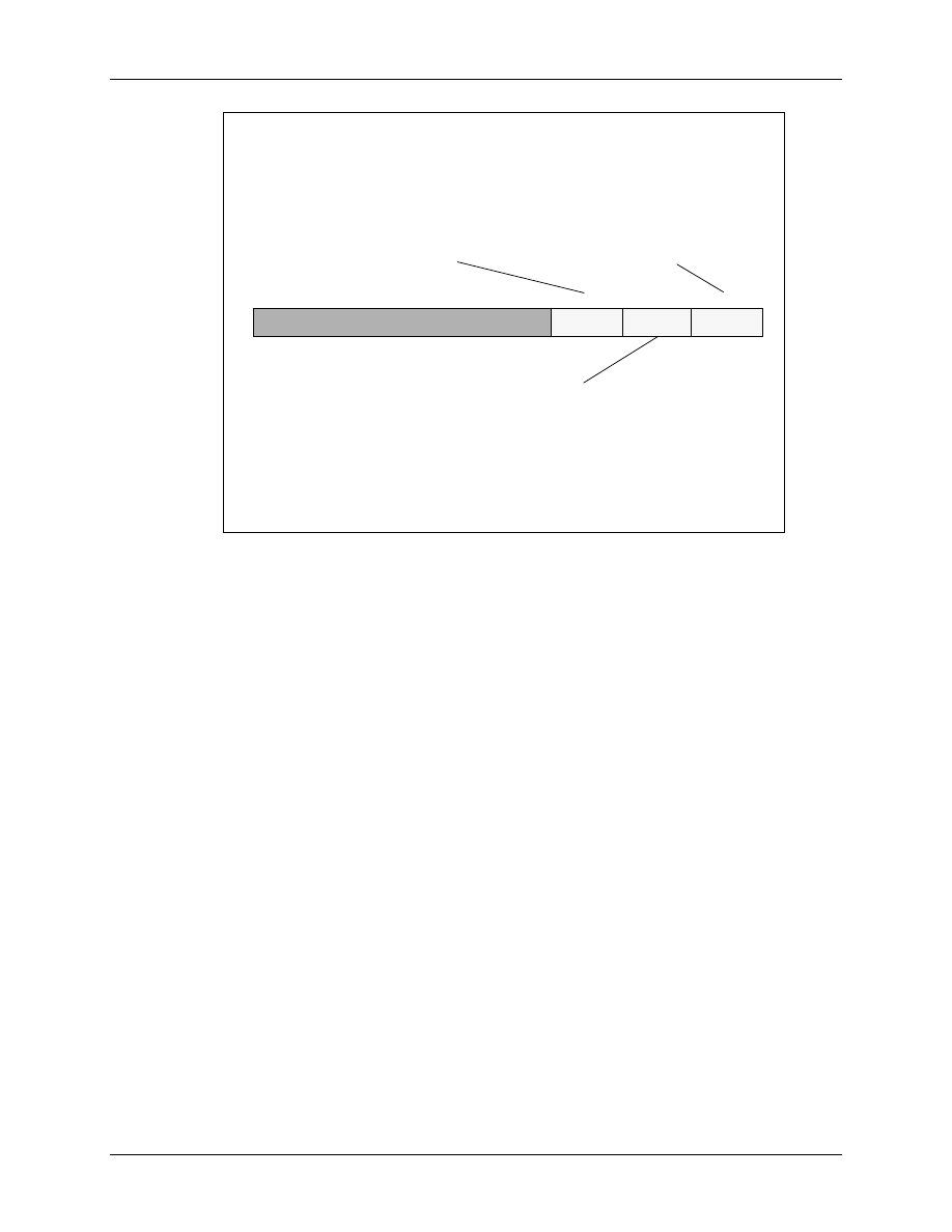
ePWM Action Qualification Unit
7 - 24
F2833x - PWM and Capture Units
ePWM Action Qualification Unit
Now let us inspect another unit, which we need to generate a series of pulses at EPWMxA and
EPWMxB - the Action Qualification Module.
7
7
-
-
18
18
ePWM Action Qualifier Module
ePWM Action Qualifier Module
16
16
-
-
Bit
Bit
Time
Time
-
-
Base
Base
Counter
Counter
Compare
Compare
Logic
Logic
Action
Action
Qualifier
Qualifier
Dead
Dead
Band
Band
PWM
PWM
Chopper
Chopper
Shadowed
Compare
Compare
Register
Register
Shadowed
Period
Period
Register
Register
Clock
Clock
Prescaler
Prescaler
Shadowed
Compare
Compare
Register
Register
CMPA . 15 - 0
CMPB . 15 - 0
TBCTR . 15 - 0
TBPRD . 15 - 0
TBCTL . 12 - 7
AQCTLB . 11 - 0
AQCTLA . 11 - 0
DBCTL . 4 - 0
PCCTL . 10 - 0
SYSCLKOUT
SYSCLKOUT
EPWMxSYNCI
EPWMxSYNCI
EPWMxSYNCO
EPWMxSYNCO
TBCLK
TBCLK
Trip
Trip
Zone
Zone
TZSEL . 15 - 0
EPWMxA
EPWMxA
EPWMxB
EPWMxB
TZy
TZy
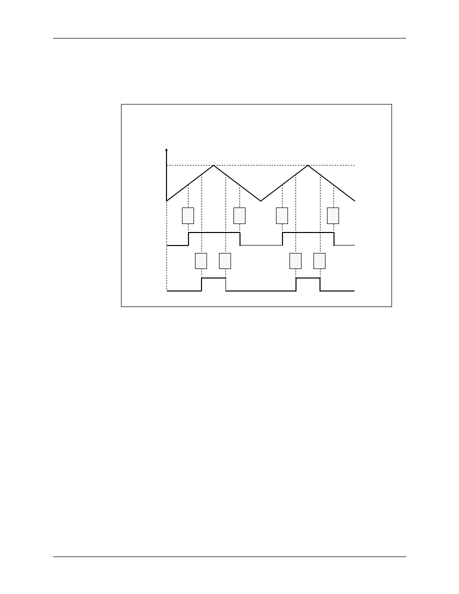
We can initialize this unit by a set of two control registers, AQCTLA for output line A and
AQCTLB for line B. For each of the 6 events on a timescale (Zero-match; CMPA-up, CMPB -
up, Period, CMPA - down and CMPB - down) we can specify a certain action at the
corresponding signal line:
• set line to high (rising edge)
• clear line to low (falling edge)
• toggle the line (low to high OR high to low)
• do nothing (ignore this event)
Furthermore we can also force the corresponding line to a certain level by executing a software
instruction in one of two software force registers. In most cases, the latter option is not used,
because it cannot be synchronized with other hardware activities of the PWM unit. Sometimes
however, especially for emergency routines, it is welcome to have such a force option.
The next slide summarizes the available options for the Action Qualification Unit. The icons used
in this slide will also be used in the following slides to highlight some popular control patterns for
PWM systems.
ePWM Action Qualification Unit
F2833x - PWM and Capture Units
7 - 25
7
7
-
-
19
19
ePWM Action Qualifier Actions
ePWM Action Qualifier Actions
Z
Z
↓
↓
Z
Z
↑
↑
Z
Z
X
X
Z
Z
T
T
CA
CA
↓
↓
CA
CA
↑
↑
CA
CA
X
X
CA
CA
T
T
CB
CB
↓
↓
CB
CB
↑
↑
CB
CB
X
X
CB
CB
T
T
P
P
↓
↓
P
P
↑
↑
P
P
X
X
P
P
T
T
SW
SW
↓
↓
SW
SW
↑
↑
SW
SW
X
X
SW
SW
T
T
Do Nothing
Do Nothing
Clear Low
Clear Low
Set High
Set High
Toggle
Toggle
S/W
S/W
Force
Force
EPWM
EPWM
Output
Output
Actions
Actions
Time
Time
-
-
Base Counter equals:
Base Counter equals:
Zero
Zero
CMPA
CMPA
CMPB
CMPB
TBPRD
TBPRD
Independent Duty Cycle on line A and B
The first example uses the lines A and B in count-up mode. The duty cycles are independently
controlled by CMPA for line A and CMPB for line B.
7
7
-
-
20
20
Independent Modulation on EPWMA / B
Independent Modulation on EPWMA / B
Z
Z
↑
↑
P
P
X
X
CB
CB
X
X
CA
CA
↓
↓
Z
Z
↑
↑
P
P
X
X
CB
CB
X
X
CA
CA
↓
↓
Z
Z
↑
↑
P
P
X
X
Z
Z
↑
↑
P
P
X
X
CB
CB
↓
↓
CA
CA
X
X
Z
Z
↑
↑
P
P
X
X
CB
CB
↓
↓
CA
CA
X
X
Z
Z
↑
↑
P
P
X
X
TBCTR
TBCTR
TBPRD
TBPRD
.
.
.
.
.
.
.
.
EPWMA
EPWMA
EPWMB
EPWMB
ePWM Action Qualification Unit
7 - 26
F2833x - PWM and Capture Units
Moving Pulse on EPWMA
This example uses EPWMB just to indicate half of the period of the PWM - frequency. CMPA
and CMPB are both used to control
(1) the position and
(2) the size of the pulse on line EPWMA
7
7
-
-
21
21
Moving Pulse on EPWMA
Moving Pulse on EPWMA
CA
CA
↑
↑
CB
CB
↓
↓
CA
CA
↑
↑
CB
CB
↓
↓
Z
Z
T
T
Z
Z
T
T
Z
Z
T
T
TBCTR
TBCTR
TBPRD
TBPRD
.
.
.
.
.
.
.
.
EPWMA
EPWMA
EPWMB
EPWMB
ePWM Action Qualification Unit
F2833x - PWM and Capture Units
7 - 27
Independent modulation of two pulses
Here both lines EPWMA and EPWMB carry a control signal. EPWMA is solely controlled by
CMPA and is always centered on the period match event. By reducing the difference between
CMPA and TBPRD we can reduce the size of the pulse, by extending the difference the pulse will
grow towards 100%.
Register CMPB is used to control the pulse size of EPWMB independently of EPWMA. In this
example output pulse EPWMB is also center aligned on the period match event.
7
7
-
-
22
22
Independent Modulation on EPWMA / B
Independent Modulation on EPWMA / B
TBCTR
TBCTR
TBPRD
TBPRD
.
.
.
.
.
.
.
.
.
.
.
.
.
.
.
.
CA
CA
↑
↑
CA
CA
↓
↓
CA
CA
↑
↑
CA
CA
↓
↓
CB
CB
↑
↑
CB
CB
↓
↓
CB
CB
↑
↑
CB
CB
↓
↓
EPWMA
EPWMA
EPWMB
EPWMB
There are many more application examples and operating modes than those, which we discussed
in the previous slides, especially when you recall typical 3-phase systems with their well known
complementary switching patterns.
Let us postpone these industrial applications for now and focus on what we have learned so far.
To perform an exercise with the basic pulse sequences shown above, we will have to include the
Action Qualification Unit (AQU) into our exercises.
We have not discussed the layout of the control registers for the AQU. The group of registers is
shown on the next slide.
ePWM Action Qualification Unit
7 - 28
F2833x - PWM and Capture Units
Action Qualification Registers
7
7
-
-
23
23
ePWM Action Qualifier Module Registers
ePWM Action Qualifier Module Registers
Name
Name
Description
Description
Structure
Structure
AQCTLA
AQCTLA
AQ Control Output A
AQ Control Output A
EPwm
EPwmx
Regs.AQCTLA.all
Regs.AQCTLA.all
=
=
AQCTLB
AQCTLB
AQ Control Output B
AQ Control Output B
EPwm
EPwmx
Regs.AQCTLB.all
Regs.AQCTLB.all
=
=
AQSFRC
AQSFRC
AQ S/W Force
AQ S/W Force
EPwm
EPwmx
Regs.AQSFRC.all
Regs.AQSFRC.all
=
=
AQCSFRC
AQCSFRC
AQ Cont. S/W Force
AQ Cont. S/W Force
EPwm
EPwmx
Regs.AQCSFRC.all
Regs.AQCSFRC.all
=
=
Action Control Register A and B
7
7
-
-
24
24
Action Qualifier Control Register
Action Qualifier Control Register
EPwm
EPwmx
Regs.AQCTL
Regs.AQCTLy (y = A or B)
ZRO
ZRO
CBU
CBU
CAD
CAD
CAU
CAU
PRD
PRD
1
1
-
-
0
0
CBD
CBD
15
15
-
-
12
12
reserved
3
3
-
-
2
2
5
5
-
-
4
4
7
7
-
-
6
6
9
9
-
-
8
8
11
11
-
-
10
10
00 = do nothing (action disabled)
00 = do nothing (action disabled)
01 = clear (low)
01 = clear (low)
10 = set (high)
10 = set (high)
11 = toggle (low
11 = toggle (low
→
→
high; high
high; high
→
→
low)
low)
Action when
Action when
CTR = CMPB
CTR = CMPB
on DOWN Count
on DOWN Count
Action when
Action when
CTR = CMPB
CTR = CMPB
on UP Count
on UP Count
Action when
Action when
CTR = CMPA
CTR = CMPA
on DOWN Count
on DOWN Count
Action when
Action when
CTR = CMPA
CTR = CMPA
on UP Count
on UP Count
Action when
Action when
CTR = 0
CTR = 0
Action when
Action when
CTR = PRD
CTR = PRD
ePWM Action Qualification Unit
F2833x - PWM and Capture Units
7 - 29
Software Forcing Registers
This register allows forcing an output line into a defined state. “One-Time” stands for the
duration of the current period of the PWM - frequency.
7
7
-
-
25
25
Action Qualifier SW Force Register
Action Qualifier SW Force Register
EPwm
EPwmx
Regs.AQSFRC
Regs.AQSFRC
ACTSFA
ACTSFA
RLDCSF
RLDCSF
OTSFB
OTSFB
ACTSFB
ACTSFB
OTSFA
OTSFA
1
1
-
-
0
0
15
15
-
-
8
8
reserved
2
2
4
4
-
-
3
3
5
5
7
7
-
-
6
6
AQSFRC Shadow Reload Options
AQSFRC Shadow Reload Options
00 = load on event CTR = 0
00 = load on event CTR = 0
01 = load on event CTR = PRD
01 = load on event CTR = PRD
10 = load on event CTR = 0 or CTR = PRD
10 = load on event CTR = 0 or CTR = PRD
11 = load immediately (from active reg.)
11 = load immediately (from active reg.)
One
One
-
-
Time S/W Force on Output B / A
Time S/W Force on Output B / A
0 = no action
0 = no action
1 = single
1 = single
s/w
s/w
force event
force event
Action on One
Action on One
-
-
Time S/W Force B / A
Time S/W Force B / A
00 = do nothing (action disabled)
00 = do nothing (action disabled)
01 = clear (low)
01 = clear (low)
10 = set (high)
10 = set (high)
11 = toggle (low
11 = toggle (low
→
→
high; high
high; high
→
→
low)
low)
“Continuous Force” will hold the line permanently in the selected state.
7
7
-
-
26
26
Continuous SW Force Register
Continuous SW Force Register
EPwmxRegs.AQCSFRC
EPwmxRegs.AQCSFRC
CSFA
CSFA
CSFB
CSFB
1
1
-
-
0
0
15
15
-
-
4
4
reserved
3
3
-
-
2
2
Continuous S/W Force on Output B / A
Continuous S/W Force on Output B / A
00 = forcing disabled
00 = forcing disabled
01 = force continuous low on output
01 = force continuous low on output
10 = force continuous high on output
10 = force continuous high on output
11 = forcing disabled
11 = forcing disabled

Lab 7_3: A 1 kHz signal with variable pulse width
7 - 30
F2833x - PWM and Capture Units
Lab 7_3: A 1 kHz signal with variable pulse width
Now let us experiment with a variable pulse width signal. The starting point is again Lab7_1. We
will now use CpuTimer0 as a time-base to change the pulse width of the 1 kHz signal once every
100 milliseconds between 0 and 100 %.
7
7
-
-
27
27
Lab 7_3: 1 KHz Signal with variable pulse
Lab 7_3: 1 KHz Signal with variable pulse
width at ePWM1A
width at ePWM1A
• Generate a 1 KHz square wave signal at ePWM1A with a
variable duty cycle between 0 and 100%
• Measure the pulse with an oscilloscope
• Registers involved:
• TBPRD:
define signal frequency
• TBCTL:
setup operating mode and time prescale
• CMPA:
setup the pulse width for ePWM1A
• AQCTLA:
define signal shape for ePWM1A
Objective:
Objective:
HSPCLKDIV
CLKDIV
T
T
TBPRD
SYSCLKOUT
PWM
∗
∗
∗
=
2
1
Objective
The objective of this lab is to generate a square wave signal of 1 kHz at line ePWM1A. With the
help of an oscilloscope connected to header J6-1 of the Peripheral Explorer Board, we can
monitor the signal. Using CPU - Timer 0, we will change CMPA between 0 and TBPRD to
generate a pulse width between 100 and 0%.
Procedure
Open Project File
1. In CCS, if not still open from Lab7_2, re-open project
Lab7.pjt.
2. Open file “Lab7_1.c” and save it as “Lab7_3.c”
3. Remove file “Lab7_2.c” from project and add “Lab7_3.c” to it. Note: optionally you can also
keep “Lab7_2.c” and exclude it from build. Use a right mouse click on file “Lab7_2.c”, select
“File Specific Options”; in category “General” enable “Exclude from Build”.
Lab 7_3: A 1 kHz signal with variable pulse width
F2833x - PWM and Capture Units
7 - 31
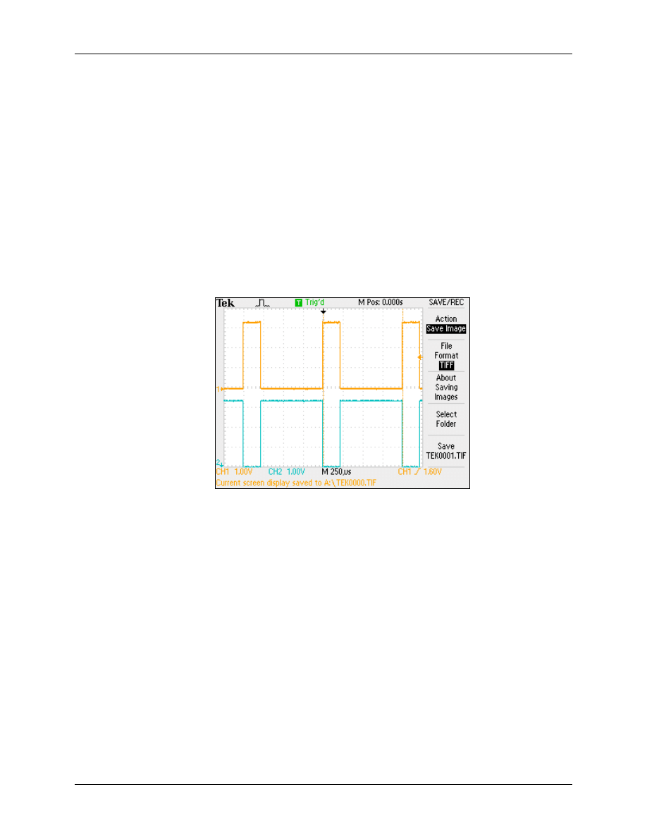
4. In file “Lab7_3.c”, edit the function “Setup_ePWM1A()”. We will again use count up/down
mode, so we can keep the existing setup for bit field TBCTL.CTRMODE. However, now we
would like to set ePWM1A to 1 on “CMPA - up match” and to clear ePWM1A on event
“CMPA - down match. Change the setup for register AQCTLA accordingly!
5. In the function “Setup_ePWM1A()” add a line to initialize CMPA to 0, which will define a
pulse width of 100%:
EPwm1Regs.CMPA.half.CMPA = 0;
6. In “main()”, change the function call “ConfigCpuTimer()” to define a period of 100
microseconds for timer 0:
ConfigCpuTimer(&CpuTimer0, 150, 100);
7. CpuTimer0 is still active from Lab exercise Lab6. It has been initialized to request an
interrupt service once every 100 microseconds. Now we can use its interrupt service routine
“cpu_timer0_isr()” to increment the value in register CMPA until it reaches the value in
TBPRD - thus we will change the pulse width gradually from 100% to 0%. If you like, you
can add a second sequence to increase the pulse width of ePWM1A again back to 100%.
Note: All registers of ePWM1 are read- and writable. To compare the current value of
CMPA against TBPRD you can use:
if (EPwm1Regs.CMPA.half.CMPA < EPwm1Regs.TBPRD) …
Build, Load and Test
7. Now build, load and test the modified project. A screenshot of signal ePWM1A could look
like this:
Result: The pulse width of your signal should change gradually between 100% and 0 %.
END of LAB 7_3

Lab 7_4: a pair of complementary 1 kHz-Signals
7 - 32
F2833x - PWM and Capture Units
Lab 7_4: a pair of complementary 1 kHz-Signals
Most power electronic systems require pairs of PWM pulse series to control two power switches
in such a way, that if one switch is on (conducting), the other switch is off (open-circuit). In the
following exercise you will modify Lab7_3 to generate such a pair of output pulses at ePWM1A
and ePWM1B. Again we will use CpuTimer0 as a time-base to change the pulse width of the 1
kHz signal every 100 milliseconds between 0 and 100 %.
7
7
-
-
28
28
Lab 7_4: a pair of complementary 1 KHz
Lab 7_4: a pair of complementary 1 KHz
signals at ePWM1A and ePWM1B
signals at ePWM1A and ePWM1B
• Generate a 1 KHz square wave signal at ePWM1A with a
variable duty cycle between 0 and 100%
• Generate a complementary signal at ePWM1B
• Measure the pulses with an oscilloscope
• Registers involved:
• TBPRD:
define signal frequency
• TBCTL:
setup operating mode and time prescale
• CMPA:
setup the pulse width for ePWM1A / 1B
• AQCTLB:
define signal shape for ePWM1B
• AQCTLA:
define signal shape for ePWM1A
Objective:
Objective:
Objective
The objective of this lab is to generate a square wave signal of 1 kHz at line ePWM1A and a
second signal at ePWM1B with opposite voltage levels. With the help of an oscilloscope
connected to header J6-1 of the Peripheral Explorer Board, we can monitor the signal. Based on
CPU - Timer 0, we will change CMPA between 0 and TBPRD to generate a pulse width between
100 and 0%.
Procedure
Open Project File
1. If not still open from Lab7_3, r-open project
Lab7.pjt
in Code Composer Studio.
2. Open file “Lab7_3.c” and save it as “Lab7_4.c”
3. Remove file “Lab7_3.c” from project and add “Lab7_4.c” to it. Note: optionally you can also
keep “Lab7_3.c” and exclude it from build. Use a right mouse click on file “Lab7_3.c”, select
“File Specific Options”; in category “General” enable “Exclude from Build”.
Lab 7_4: a pair of complementary 1 kHz-Signals
F2833x - PWM and Capture Units
7 - 33
4. In file “Lab7_4.c” edit function “Gpio_select()”. In the multiplex block enable line GPIO1 to
drive ePWM1B.
5. Rename function “Setup_ePWM1A()” to “Setup_ePWM1()”, because we will now initialize
both line A and B with this function. Also, rename the function prototype at the beginning of
“Lab7_4.c” and the function call in “main()”.
6. In “Setup_ePWM1()”, add a line to initialize register EPwm1Regs.AQCTLB. Recall that we
initialized EPwm1Regs.AQCTLA to set ePWM1A on CMPA - up and to clear ePWM1A on
CMPA - down match. For register EPwm1Regs.AQCTLB we will have to modify that setup
to generate a complementary signal at ePWM1B.
Build, Load and Test
7. Now build, load and test the modified project. A oscilloscope screenshot of signal ePWM1A
and ePWM1B should look like this:
Result: The pulse width of your pair of signals should change gradually between 100% and 0
%.
END of LAB 7_4
Lab 7_5: Independent Modulation on ePWM1A / 1B
7 - 34
F2833x - PWM and Capture Units
Lab 7_5: Independent Modulation on ePWM1A / 1B
Before we continue to discuss other modules of the ePWM - units we will perform an exercise to
produce the exact pulse pattern, as shown in Slide 7-29:
7
7
-
-
29
29
Lab 7_5: Independent Modulation of
Lab 7_5: Independent Modulation of
ePWM1A and ePWM1B
ePWM1A and ePWM1B
TBCTR
TBCTR
TBPRD
TBPRD
.
.
.
.
.
.
.
.
.
.
.
.
.
.
.
.
CA
CA
↑
↑
CA
CA
↓
↓
CA
CA
↑
↑
CA
CA
↓
↓
CB
CB
↑
↑
CB
CB
↓
↓
CB
CB
↑
↑
CB
CB
↓
↓
EPWMA
EPWMA
EPWMB
EPWMB
Objective
The objective of this lab is to generate a square wave signal of 1 kHz at line ePWM1A and a
second signal at ePWM1B with independent modulation of the pulse widths. Signal ePWM1A
will be controlled by register CMPA and ePWM1B by register CMPB. This time we will also use
a real-time operating mode to change the values of CMPA and CMPB in a variable watch
window while the program is running.
Procedure
Open Project File
1. If not still open from Lab7_4, re-open project
Lab7.pjt
in Code Composer Studio.
2. Open file “Lab7_4.c” and save it as “Lab7_5.c”
3. Remove file “Lab7_4.c” from project and add “Lab7_5.c” to it. Note: optionally you can also
keep “Lab7_4.c” and exclude it from build. Use a right mouse click on file “Lab7_4.c”, select
“File Specific Options”; in category “General” enable “Exclude from Build”.
Lab 7_5: Independent Modulation on ePWM1A / 1B
F2833x - PWM and Capture Units
7 - 35
4. In
the
function
“Setup_ePWM1()”,
change the line to initialize register
EPwm1Regs.AQCTLB. The new setup for AQCTLB should be to set ePWM1B on CMPB -
up and to clear ePWM1B on CMPB - down match.
5. After the line to initialize register TBPRD, add two lines to set register CMPA and CMPB to
initially generate a pulse width of 50%.
EPwm1Regs.CMPA.half.CMPA = EPwm1Regs.TBPRD / 2;
EPwm1Regs.CMPB = EPwm1Regs.TBPRD / 2;
Note the difference between the structure data types of the two registers. This difference is
caused by a second operating mode, called “High Resolution PWM” (HRPWM), which is
available only for the signal line(s) ePWMxA. To support this mode, TI has enhanced the
structure type for register CMPA.
6. In the function “cpu_timer0_isr()”, remove all instructions to change the pulse width by
register CMPA. We will use a fixed pulse width for this exercise, initially 50% for both
ePWM1A and ePWM1B.
Build, Load and Test
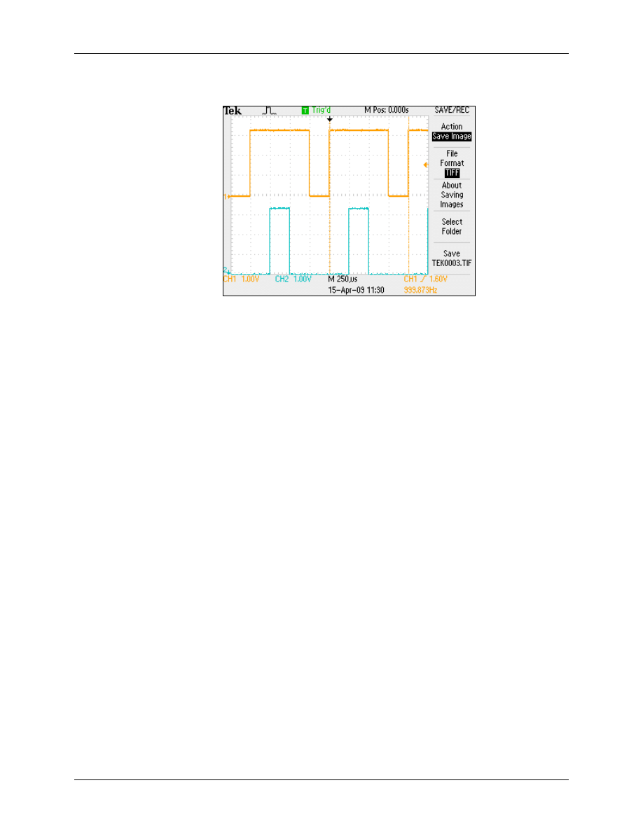
7. Now build, load and test the modified project. A oscilloscope screenshot of signal ePWM1A
and ePWM1B should look like this:
8. Stop the code execution:
Debug
Halt, followed by
Debug
Reset CPU
9. Now open a Watch Window:
View
Watch Window
In window “Watch 1” add the two variables:
EPwm1Regs.CMPA.half.CMPA and
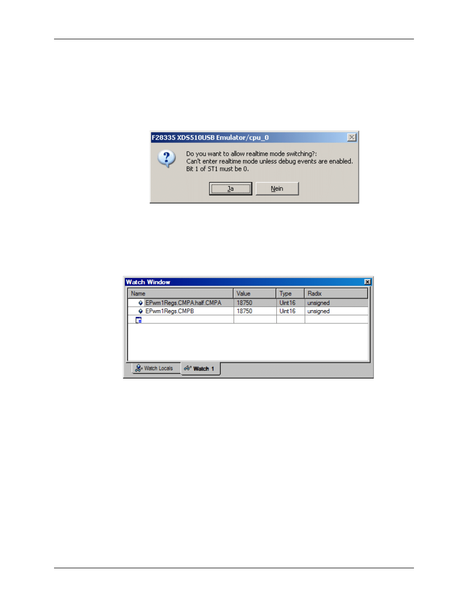
Lab 7_5: Independent Modulation on ePWM1A / 1B
7 - 36
F2833x - PWM and Capture Units
EPwm1Regs.CMPB
10. Enable Real Time Debug Mode:
Debug Real-time Mode
A warning might pop up on your screen to inform you, that you will enter a real time data
exchange debug mode now. Answer this window with “Yes”:
Right mouse click in the Watch window and select “Continuous Refresh”
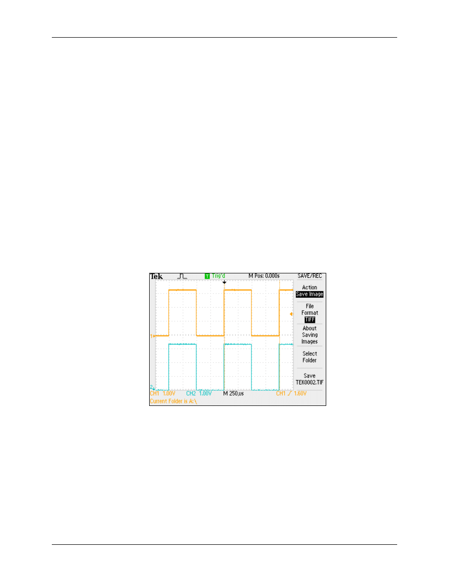
11. Restart your Test, this time with a new sequence:
GEL
Realtime Emulation Control Run_Realtime_with_Restart
Your Watch window should display the current values for CMPA and CMPB, e.g.:
Now, while the code is still running, change the values in CMPA and CMPB to 9375 and
28125 respectively.
Lab 7_5: Independent Modulation on ePWM1A / 1B
F2833x - PWM and Capture Units
7 - 37
The result should look like this:
Try other combinations of CMPA and CMPB and verify the changes with your scope!
12. If you are done with this exercise, it is important to fully halt the DSC. Since we are currently
running in real time mode, we have to apply a different command sequence:
GEL
Realtime Emulation Control Full_Halt_with_Reset
END of LAB 7_5
ePWM Dead Band Module
7 - 38
F2833x - PWM and Capture Units
ePWM Dead Band Module
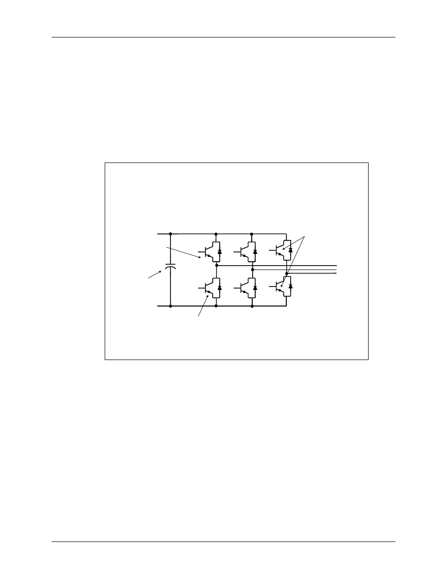
Motivation for Dead - Band
In switched mode power electronics, a typical configuration to drive a 3-phase system is shown in
the next slide (Slide 7-30). A typical system consists of a 3-phase current or voltage injection
circuit, in which a pair of power switches per phase is controlled by a sequence of PWM - pulses.
A phase current flows either from a DC bus voltage through a top switch into the winding of a
motor or via a bottom switch from the motor winding back to ground. Of course, we have to
prevent both switches from conducting at the same time.
7
7
-
-
30
30
Power
Switching
Devices
Three phase
outputs to drive
the motor
terminals
+
−
Upper & lower
devices can not
be turned on
simultaneously
(dead band)
PWM signal is
applied between
gate and source
DC bus
capacitor
Voltage source inverter components
Voltage source inverter components
+
+
−
−
A minor problem arises from the fact that power switches usually turn on faster than they turn off.
If we would apply an identical but complementary pulse pattern to the top and bottom switch of a
phase, we would end up in a short period in time with a shoot-through situation.
Dead-band control provides a convenient means of combating current “shoot-through” problems
in a power converter. “Shoot-through” occurs when both the upper and lower transistors in the
same phase of a power converter are on simultaneously. This condition shorts the power supply
and results in a large current draw. Shoot-through problems occur because transistors (especially
FET’s) turn on faster than they turn off and also because high-side and low-side power converter
transistors are typically switched in a complimentary fashion. Although the duration of the shoot-
through current path is finite during PWM cycling, (i.e. the transistor will eventually turn off),
even brief periods of a short circuit condition can produce excessive heating and stress the power
converter and power supply.
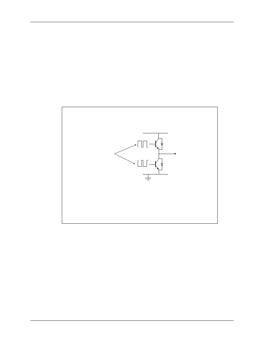
ePWM Dead Band Module
F2833x - PWM and Capture Units
7 - 39
Two basic approaches exist for controlling shoot-through: modify the transistors, or modify the
PWM gate signals controlling the transistors. In the first case, the switch-on time of the transistor
gate must be increased so that it (slightly) exceeds the switch-off time.
The hard way to accomplish this is by adding a cluster of passive components such as resistors
and diodes in series with the transistor gate to act as low-pass filter to implement the delay.
The second approach to shoot-through control separates transitions on complimentary PWM
signals with a fixed period of time. This is called dead-band. While it is possible to perform
software implementation of dead-band, the F2833x offers on-chip hardware for this purpose that
requires no additional CPU overhead. Compared to the passive approach, dead-band offers more
precise control of gate timing requirements.
7
7
-
-
31
31
Motivation for Dead
Motivation for Dead
-
-
Band
Band
to power
switching
device
supply rail
gate signals are
complementary PWM
♦ Transistor gates turn on faster than they shut off
♦ Short circuit if both gates are on at same time!
ePWM Dead Band Module
7 - 40
F2833x - PWM and Capture Units
Hardware Dead Band Unit
All ePWM modules of the F2833x feature a hardware dead band unit.
7
7
-
-
32
32
ePWM Dead
ePWM Dead
-
-
Band Module
Band Module
16
16
-
-
Bit
Bit
Time
Time
-
-
Base
Base
Counter
Counter
Compare
Compare
Logic
Logic
Action
Action
Qualifier
Qualifier
Dead
Dead
Band
Band
PWM
PWM
Chopper
Chopper
Shadowed
Compare
Compare
Register
Register
Shadowed
Period
Period
Register
Register
Clock
Clock
Prescaler
Prescaler
Shadowed
Compare
Compare
Register
Register
CMPA . 15 - 0
CMPB . 15 - 0
TBCTR . 15 - 0
TBPRD . 15 - 0
TBCTL . 12 - 7
AQCTLB . 11 - 0
AQCTLA . 11 - 0
DBCTL . 4 - 0
PCCTL . 10 - 0
SYSCLKOUT
SYSCLKOUT
EPWMxSYNCI
EPWMxSYNCI
EPWMxSYNCO
EPWMxSYNCO
TBCLK
TBCLK
Trip
Trip
Zone
Zone
TZSEL . 15 - 0
EPWMxA
EPWMxA
EPWMxB
EPWMxB
TZy
TZy
The block diagram shows the different options available for this module:
7
7
-
-
33
33
ePWM Dead
ePWM Dead
-
-
Band Module Block Diagram
Band Module Block Diagram
Rising
Rising
Edge
Edge
Delay
Delay
In Out
(10
(10
-
-
bit
bit
counter)
counter)
Falling
Falling
Edge
Edge
Delay
Delay
In Out
(10
(10
-
-
bit
bit
counter)
counter)
°
°
°
°
°
°
0
1
°
°
°
°
°
°
0
1
°
°
°
°
°
°
0
1
°
°
°
°
°
°
1
0
°
°
°
°
.
.
.
.
PWMxA
PWMxA
-
-
IN
IN
PWMxB
PWMxB
-
-
IN
IN
PWMxB
PWMxB
PWMxA
PWMxA
S1
S0
S2
S3
FED
RED
OUT
OUT
-
-
MODE
MODE
POLSEL
POLSEL
°
°
°
°
°
°
0
1
°
°
°
°
°
°
0
1
S4
S5
IN
IN
-
-
MODE
MODE
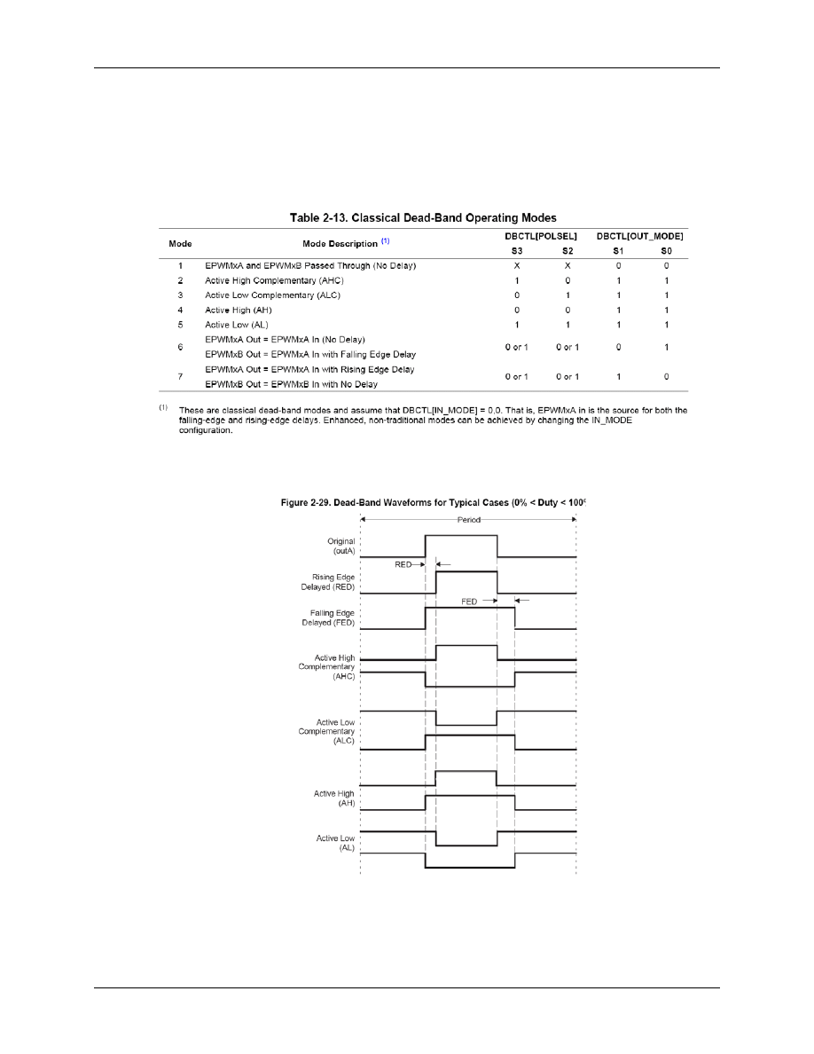
ePWM Dead Band Module
F2833x - PWM and Capture Units
7 - 41
The setup of the dead-band unit is based on six switches, S0 to S5.
Although all combinations are supported, not all modes would be used in practice. The more
classical modes assume that S4=0 and S5=0 [IN_MODE] is configured such that “EPWMxA-IN”
is the source for both the falling-edge and rising-edge delay. Enhanced or non-traditional modes
can be achieved by changing the input signal source.
The corresponding pulse sequences are:
Operating mode “Active High Complementary” (AHC) is the desired one for a pair of power
switches in one phase of a 3-phase motor control system.
ePWM Dead Band Module
7 - 42
F2833x - PWM and Capture Units
Dead Band Unit Registers
7
7
-
-
34
34
ePWM Dead
ePWM Dead
-
-
Band Module Registers
Band Module Registers
Rising Edge Delay = T
Rising Edge Delay = T
TBCLK
TBCLK
x DBRED
x DBRED
Falling Edge Delay = T
Falling Edge Delay = T
TBCLK
TBCLK
x DBFED
x DBFED
Name
Name
Description
Description
Structure
Structure
DBCTL
DBCTL
Dead
Dead
-
-
Band Control
Band Control
EPwm
EPwmx
Regs.DBCTL.all
Regs.DBCTL.all
=
=
DBRED
DBRED
10
10
-
-
bit Rising Edge Delay
bit Rising Edge Delay
EPwm
EPwmx
Regs.DBRED
Regs.DBRED
=
=
DBFED
DBFED
10
10
-
-
bit Falling Edge Delay
bit Falling Edge Delay
EPwm
EPwmx
Regs.DBFED
Regs.DBFED
=
=
The Dead Band Control Register combines the bit fields for switches S0 to S5:
7
7
-
-
35
35
ePWM Dead Band Control Register
ePWM Dead Band Control Register
Polarity Select
Polarity Select
00 = active high
00 = active high
01 = active low complementary (RED)
01 = active low complementary (RED)
10 = active high complementary (FED)
10 = active high complementary (FED)
11 = active low
11 = active low
Out
Out
-
-
Mode Control
Mode Control
00 = disabled (DBM bypass)
00 = disabled (DBM bypass)
01 =
01 =
PWMxA
PWMxA
= no delay
= no delay
PWMxB
PWMxB
= FED
= FED
10 =
10 =
PWMxA
PWMxA
= RED
= RED
PWMxB
PWMxB
= no delay
= no delay
11 = RED & FED (DBM fully enabled)
11 = RED & FED (DBM fully enabled)
OUT_MODE
OUT_MODE
POLSEL
POLSEL
1
1
-
-
0
0
15
15
-
-
6
6
reserved
3
3
-
-
2
2
IN_MODE
IN_MODE
5
5
-
-
4
4
In
In
-
-
Mode Control
Mode Control
00 =
00 =
PWMxA
PWMxA
is source for RED and FED
is source for RED and FED
01 =
01 =
PWMxA
PWMxA
is source for FED
is source for FED
PWMxB
PWMxB
is source for RED
is source for RED
10 =
10 =
PWMxA
PWMxA
is source for RED
is source for RED
PWMxB
PWMxB
is source for FED
is source for FED
11 =
11 =
PWMxB
PWMxB
is source for RED and FED
is source for RED and FED

Lab 7_6: Dead Band Unit on ePWM1A / 1B
F2833x - PWM and Capture Units
7 - 43
Lab 7_6: Dead Band Unit on ePWM1A / 1B
Objective
The objective of this lab is to introduce a delay time for rising edges in a pair of complementary
PWM signals at ePWM1A and ePWM1B. The desired operating mode is “Active High
Complementary” (AHC) and the two output signals are generated from input signal ePWM1A -
in from the action qualifier unit.
7
7
-
-
36
36
Lab 7_6: Dead Band Unit for
Lab 7_6: Dead Band Unit for
ePWM1A and ePWM1B
ePWM1A and ePWM1B
• Add a delay time for rising edges on a pair of
complementary signals ePWM1A and ePWM1B
• Active High Complementary (AHC) Mode
• Input signal to Dead-Band Unit is ePWM1A
• Dead Band Unit will generate ePWM1A and ePWM1B
• Use Lab7_4 as starting point
• New Registers involved:
• DBRED:
Dead Band Unit Rising Edge Delay
• DBFED:
Dead Band Unit Falling Edge Delay
• DBCTL:
Dead Band Unit Control Register
Objective:
Objective:
Procedure
Open Project File
1. If not still open from Lab7_5, re-open project
Lab7.pjt
in Code Composer Studio.
2. Open file “Lab7_4.c” and save it as “Lab7_6.c”
3. Add “Lab7_6.c” to the project and exclude “Lab7_5.c” from build. Use a right mouse click
on file “Lab7_5.c”, select “File Specific Options”; in category “General” enable “Exclude
from Build”.
4. In the function “cpu_timer0_isr()”, remove all instructions to change the pulse width by
register CMPA. We will use a fixed pulse width of 50% for this exercise, both for ePWM1A
and ePWM1B.
5. In the function “Setup_ePWM1()”, initialize the pulse width to 50% of TBPRD:
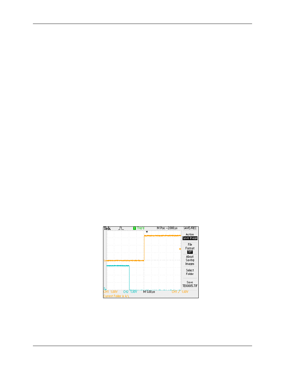
Lab 7_6: Dead Band Unit on ePWM1A / 1B
7 - 44
F2833x - PWM and Capture Units
EPwm1Regs.CMPA.half.CMPA = EPwm1Regs.TBPRD / 2;
6. Next, in the function “Setup_ePWM1()”, remove the instruction to initialize register
AQCTLB. When using the dead band unit, both output pulse sequences ePWM1A and
ePWM1B are normally derived from a single input signal, usually from internal signal
ePWM1A of the action qualifier module.
7. In the function “Setup_ePWM1()”, add lines to initialize the dead band unit. Delay times are
calculated in multiples of TBCLK, which we calculated at the beginning of Lab7_1 directly
from SYSCLKOUT with CLKDIV set to 1 and HSPCLKDIV set to 2. In case of the
F28335ControlCard running at 150MHz, TBCLK equals to 13.33334 ns. In our example we
will setup a delay time of 10 microseconds, just as an example.
EPwm1Regs.DBRED = 750;
EPwm1Regs.DBFED = 750;
To initialize register DBCTL, we have to take into account switches S0 to S5 in Slide 7-33:
• Set S4 and S5 to 0: this way we will solely use input signal ePWM1A from unit
AQCTL to generate the two output signals ePWM1A and ePWM1B.
• Set S2 = 0 and S3=1 to invert the polarity of signal ePWM1B against input
ePWM1A.
• Set S0 = 1 and S1 = 1 to include a time delay for both switching points
Build, Load and Test
8. Now build, load and test the modified project. A oscilloscope screenshot of signal ePWM1A
and ePWM1B should look like this, when you trigger at the rising edge of channel 1
(ePWM1A):
If you trigger at the falling edge of channel 1 (ePWM1A, yellow), again you should see a
delayed rising edge, now at signal ePWM1B (blue):
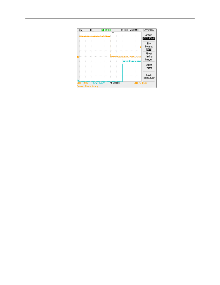
Lab 7_6: Dead Band Unit on ePWM1A / 1B
F2833x - PWM and Capture Units
7 - 45
END of LAB 7_6
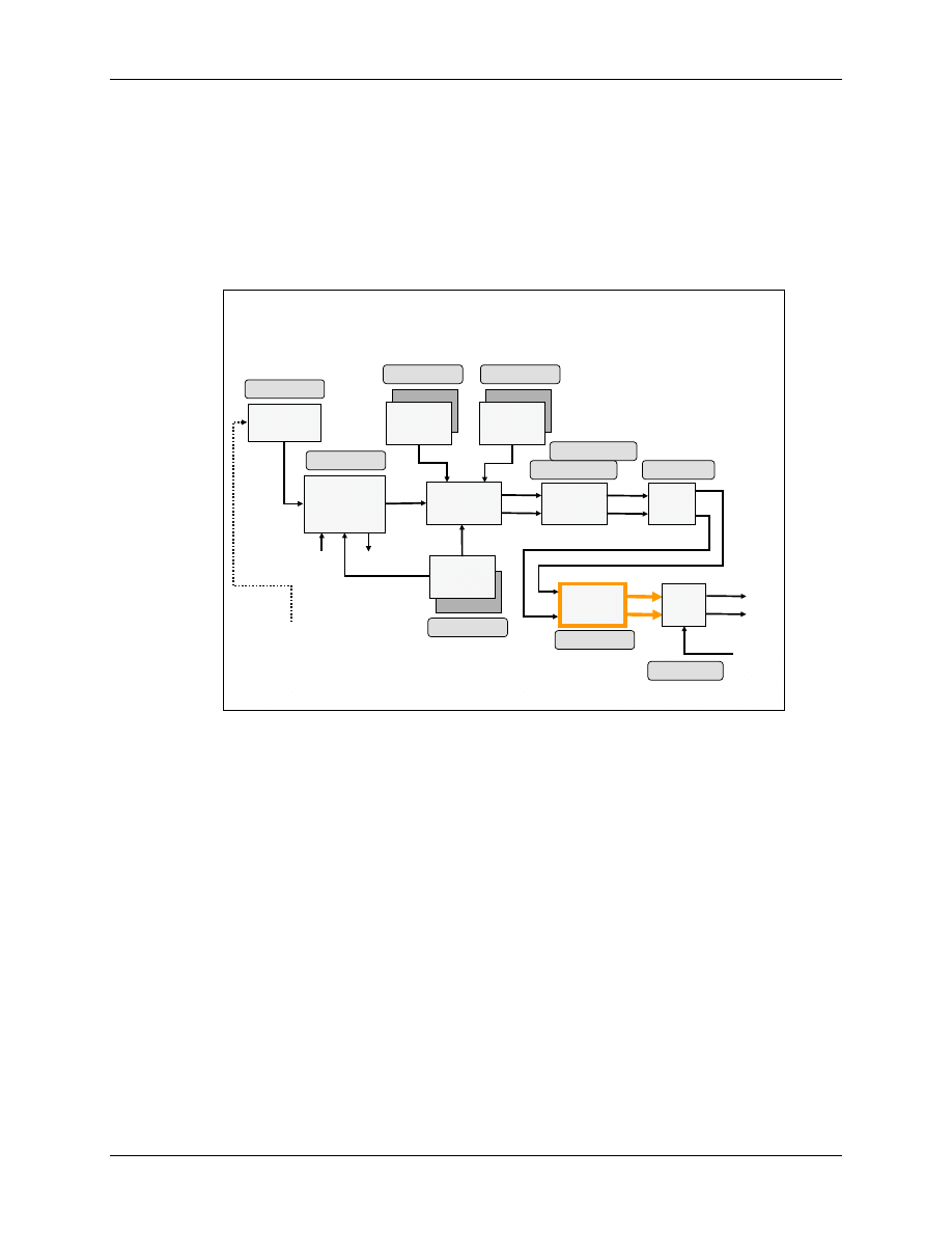
ePWM Chopper Module
7 - 46
F2833x - PWM and Capture Units
ePWM Chopper Module
The PWM-chopper sub module allows a high-frequency carrier signal to modulate the PWM
waveform generated by the action-qualifier and dead-band sub modules. This capability is
important if you need pulse transformer-based gate drivers to control the power switching
elements.
7
7
-
-
37
37
ePWM
ePWM
Chopper Module
Chopper Module
16
16
-
-
Bit
Bit
Time
Time
-
-
Base
Base
Counter
Counter
Compare
Compare
Logic
Logic
Action
Action
Qualifier
Qualifier
Dead
Dead
Band
Band
PWM
PWM
Chopper
Chopper
Shadowed
Compare
Compare
Register
Register
Shadowed
Period
Period
Register
Register
Clock
Clock
Prescaler
Prescaler
Shadowed
Compare
Compare
Register
Register
CMPA . 15 - 0
CMPB . 15 - 0
TBCTR . 15 - 0
TBPRD . 15 - 0
TBCTL . 12 - 7
AQCTLB . 11 - 0
AQCTLA . 11 - 0
DBCTL . 4 - 0
PCCTL . 10 - 0
SYSCLKOUT
SYSCLKOUT
EPWMxSYNCI
EPWMxSYNCI
EPWMxSYNCO
EPWMxSYNCO
TBCLK
TBCLK
Trip
Trip
Zone
Zone
TZSEL . 15 - 0
EPWMxA
EPWMxA
EPWMxB
EPWMxB
TZy
TZy
The key functions of the PWM-chopper sub module are:
•
Programmable chopping (carrier) frequency
•
Programmable pulse width of first pulse
•
Programmable duty cycle of second and subsequent pulses
•
Can be fully bypassed if not required

ePWM Chopper Module
F2833x - PWM and Capture Units
7 - 47
Purpose of Chopping
7
7
-
-
38
38
Purpose of the PWM Chopper Module
Purpose of the PWM Chopper Module
Allows a high frequency carrier
Allows a high frequency carrier
signal to modulate the PWM
signal to modulate the PWM
waveform generated by the Action
waveform generated by the Action
Qualifier and Dead
Qualifier and Dead
-
-
Band modules
Band modules
Used with pulse transformer
Used with pulse transformer
-
-
based
based
gate drivers to control power
gate drivers to control power
switching elements
switching elements
The carrier clock of the ePWM Chopper Module is derived from SYSCLKOUT. The frequency
and duty cycle of the chopper unit are controlled via the CHPFREQ and CHPDUTY bits in the
PCCTL register.
The one-shot block is a feature that provides a high-energy first pulse to ensure hard and fast
power switch turn on, while the subsequent pulses sustain pulses, ensuring the power switch
remains on. The one-shot width is programmed via the OSHTWTH bits.
The PWM-chopper sub module can be fully disabled (bypassed) via the CHPEN bit.
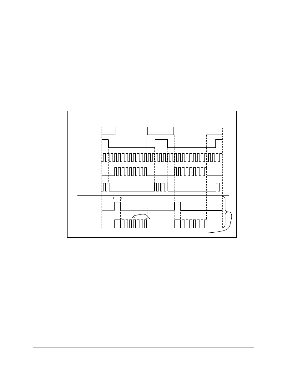
ePWM Chopper Module
7 - 48
F2833x - PWM and Capture Units
Waveform Diagram of Chopped Signals
The top half of the following slide (Slide 7-39) shows the simplified waveforms of the chopping
module action.
The bottom part of this slide shows a diagram of the special "one shot" mode, in which the
duration of the first pulse can be programmed independently of all sustaining pulses of the
chopper sequence.
Note: The duty-cycle control mode of the chopper module is not shown in the slide. This
additional mode allows the setup of a different pulse width other than 50%.
7
7
-
-
39
39
ePWM
ePWM
Chopper Waveform
Chopper Waveform
EPWMxA
EPWMxA
EPWMxB
EPWMxB
CHPFREQ
CHPFREQ
EPWMxA
EPWMxA
EPWMxB
EPWMxB
OSHT
OSHT
EPWMxA
EPWMxA
Programmable
Pulse Width
(OSHTWTH)
Sustaining
Pulses
With One-Shot Pulse on EPWMxA and/or EPWMxB
The width of the first pulse can be programmed to any of 16 possible pulse width values. The
width or period of the first pulse is given by:
OSHTWTH
T
T
SYSCLKOUT
stPULSE
∗
∗
=
8
1
Where T
SYSCLKOUT
is the period of the system clock (SYSCLKOUT) and OSHTWTH is set by
four control bits to a value between 1 and 16.
ePWM Chopper Module
F2833x - PWM and Capture Units
7 - 49
Chopper Mode Control Registers
7
7
-
-
40
40
ePWM
ePWM
Chopper Module Registers
Chopper Module Registers
Name
Name
Description
Description
Structure
Structure
PCCTL
PCCTL
PWM
PWM
-
-
Chopper Control
Chopper Control
EPwm
EPwmx
Regs.PCCTL.all
Regs.PCCTL.all
=
=
7
7
-
-
41
41
ePWM
ePWM
Chopper Control Register
Chopper Control Register
EPwm
EPwmx
Regs.PCCTL
Regs.PCCTL
CHPEN
CHPEN
CHPDUTY
CHPDUTY
CHPFREQ
CHPFREQ
OSHTWTH
OSHTWTH
0
0
15
15
-
-
11
11
reserved
4
4
-
-
1
1
7
7
-
-
5
5
10
10
-
-
8
8
Chopper Enable
Chopper Enable
0 = disable (bypass)
0 = disable (bypass)
1 = enable
1 = enable
One
One
-
-
Shot Pulse Width
Shot Pulse Width
0000 = 8 / SYSCLKOUT
0000 = 8 / SYSCLKOUT
1000 = 72 / SYSCLKOUT
1000 = 72 / SYSCLKOUT
0001 = 16 / SYSCLKOUT
0001 = 16 / SYSCLKOUT
1001 = 80 / SYSCLKOUT
1001 = 80 / SYSCLKOUT
0010 = 24 / SYSCLKOUT
0010 = 24 / SYSCLKOUT
1010 = 88 / SYSCLKOUT
1010 = 88 / SYSCLKOUT
0011 = 32 / SYSCLKOUT
0011 = 32 / SYSCLKOUT
1011 = 96 / SYSCLKOUT
1011 = 96 / SYSCLKOUT
0100 = 40 / SYSCLKOUT
0100 = 40 / SYSCLKOUT
1100 = 104 / SYSCLKOUT
1100 = 104 / SYSCLKOUT
0101 = 48 / SYSCLKOUT
0101 = 48 / SYSCLKOUT
1101 = 112 / SYSCLKOUT
1101 = 112 / SYSCLKOUT
0110 = 56 / SYSCLKOUT
0110 = 56 / SYSCLKOUT
1110 = 120 / SYSCLKOUT
1110 = 120 / SYSCLKOUT
0111 = 64 / SYSCLKOUT
0111 = 64 / SYSCLKOUT
1111 = 128 / SYSCLKOUT
1111 = 128 / SYSCLKOUT
Chopper
Chopper
Clk
Clk
Freq.
Freq.
000 = SYSCLKOUT/8
000 = SYSCLKOUT/8
÷
÷
1
1
001 = SYSCLKOUT/8
001 = SYSCLKOUT/8
÷
÷
2
2
010 = SYSCLKOUT/8
010 = SYSCLKOUT/8
÷
÷
3
3
011 = SYSCLKOUT/8
011 = SYSCLKOUT/8
÷
÷
4
4
100 = SYSCLKOUT/8
100 = SYSCLKOUT/8
÷
÷
5
5
101 = SYSCLKOUT/8
101 = SYSCLKOUT/8
÷
÷
6
6
110 = SYSCLKOUT/8
110 = SYSCLKOUT/8
÷
÷
7
7
111 = SYSCLKOUT/8
111 = SYSCLKOUT/8
÷
÷
8
8
Chopper
Chopper
Clk
Clk
Duty Cycle
Duty Cycle
000 = 1/8 (12.5%)
000 = 1/8 (12.5%)
001 = 2/8 (25.0%)
001 = 2/8 (25.0%)
010 = 3/8 (37.5%)
010 = 3/8 (37.5%)
011 = 4/8 (50.0%)
011 = 4/8 (50.0%)
100 = 5/8 (62.5%)
100 = 5/8 (62.5%)
101 = 6/8 (75.0%)
101 = 6/8 (75.0%)
110 = 7/8 (87.5%)
110 = 7/8 (87.5%)
111 = reserved
111 = reserved
Lab 7_7: Chopped Signals at ePWM1A / 1B
7 - 50
F2833x - PWM and Capture Units
Lab 7_7: Chopped Signals at ePWM1A / 1B
Objective
We will add a chopper frequency modulation to the software developed in Chapter 7. In Lab7_5
we controlled the pulse width of ePWM1A by register CMPA independently of ePWM1B, which
was controlled by CMPB. The objective now is to chop the active phase of the pulses at
ePWM1A and ePWM1B with a higher frequency.
7 - 42
Lab 7_7: Chopper Mode Signals
add ePWM1A and ePWM1B
• The pair of complementary signals ePWM1A and ePWM1B
will be modulated by a chopper frequency of 2.344 MHz
• Chopper Mode Duty Cycle = 50%
• One shot pulse width = 800 ns
• Use Lab7_5 as starting point
Objective:
Procedure
Open Project File
1. In project "Lab7" open file “Lab7_5.c” and save it as “Lab7_7.c”
2. Add “Lab7_7.c” to the project and exclude “Lab7_6.c” from build. Use a right mouse click
on file “Lab7_6.c”, select “File Specific Options”; in category “General” enable “Exclude
from Build”.
3. In the function “Setup_ePWM1()”, initialize the chopper module. Remember that
SYSCLKOUT has been set to 150 MHz (assuming an external clock of 30 MHz at the
F28335ControlCard). In register "EPwm1Regs.PCCTL":
•
Set chopper frequency to 2.34375 MHz (SYSCLKOUT / 64).
•
Set chopper duty cycle to 50%
•
Set one shot pulse to 800 ns
•
Enable the chopper unit.
Lab 7_7: Chopped Signals at ePWM1A / 1B
F2833x - PWM and Capture Units
7 - 51
Build, Load and Test
4. Build, load and test the modified project. A oscilloscope screenshot of signal ePWM1A and
ePWM1B should look like this, when you trigger at the rising edge of channel 1 (ePWM1A):
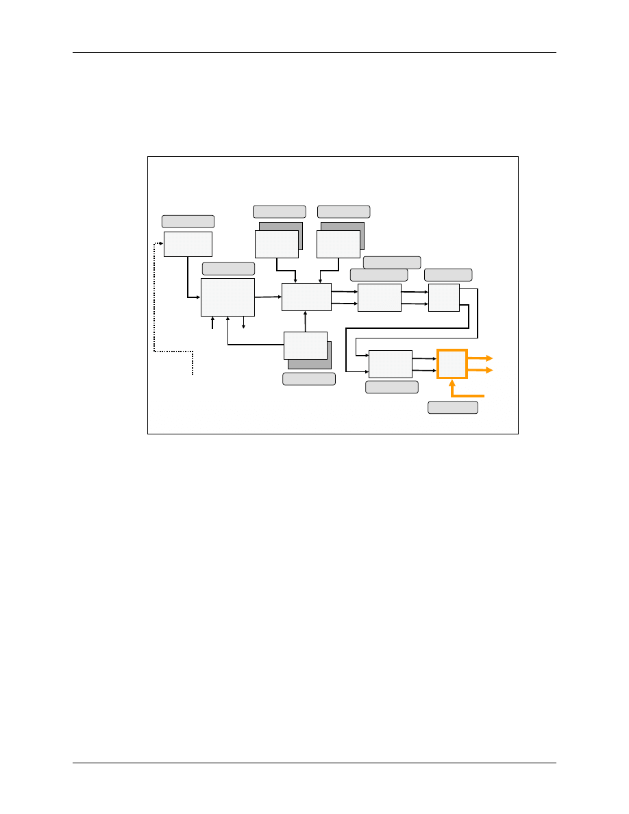
ePWM Over Current Protection
7 - 52
F2833x - PWM and Capture Units
ePWM Over Current Protection
Each ePWM module is connected to six Trip - Zone signals (TZ1 to TZ6) that are sourced from
the GPIO MUX. These signals indicate external fault or trip conditions, and the ePWM outputs
can be programmed to respond accordingly when faults occur.
7
7
-
-
43
43
ePWM
ePWM
Trip
Trip
-
-
Zone Module
Zone Module
16
16
-
-
Bit
Bit
Time
Time
-
-
Base
Base
Counter
Counter
Compare
Compare
Logic
Logic
Action
Action
Qualifier
Qualifier
Dead
Dead
Band
Band
PWM
PWM
Chopper
Chopper
Shadowed
Compare
Compare
Register
Register
Shadowed
Period
Period
Register
Register
Clock
Clock
Prescaler
Prescaler
Shadowed
Compare
Compare
Register
Register
CMPA . 15 - 0
CMPB . 15 - 0
TBCTR . 15 - 0
TBPRD . 15 - 0
TBCTL . 12 - 7
AQCTLB . 11 - 0
AQCTLA . 11 - 0
DBCTL . 4 - 0
PCCTL . 10 - 0
SYSCLKOUT
SYSCLKOUT
EPWMxSYNCI
EPWMxSYNCI
EPWMxSYNCO
EPWMxSYNCO
TBCLK
TBCLK
Trip
Trip
Zone
Zone
TZSEL . 15 - 0
EPWMxA
EPWMxA
EPWMxB
EPWMxB
TZy
TZy
Purpose of the Trip-Zone Submodule
Trip Zone signals are usually generated by over-current sensors, which set a signal if a threshold
is passed. The key functions of the Trip-Zone sub module are:
•
Trip inputs TZ1 to TZ6 can be flexibly mapped to any ePWM module.
•
Upon a fault condition, outputs EPWMxA and EPWMxB can be forced to one of the
following:
High
Low
High-impedance
No action taken
•
One-shot trip (OSHT) mode to support major short circuits or over-current
conditions.
•
Support for cycle-by-cycle tripping (CBC) for current limiting operation.
•
Each trip-zone input pin can be allocated to either one-shot or cycle-by-cycle
operation.
•
Interrupt generation is possible on any trip-zone pin.
•
Software-forced tripping is also supported.
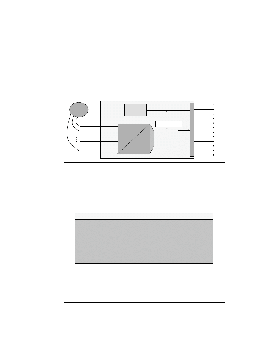
ePWM Over Current Protection
F2833x - PWM and Capture Units
7 - 53
•
The trip-zone sub module can be fully bypassed if it is not required.
7
7
-
-
44
44
Trip
Trip
-
-
Zone Module Features
Zone Module Features
♦
♦
Trip
Trip
-
-
Zone has a fast, clock independent logic path to high
Zone has a fast, clock independent logic path to high
-
-
impedance
impedance
the
the
EPWMxA
EPWMxA
/B output pins
/B output pins
♦
♦
Interrupt latency may not protect hardware when responding to ov
Interrupt latency may not protect hardware when responding to ov
er
er
current conditions or short
current conditions or short
-
-
circuits through ISR software
circuits through ISR software
♦
♦
Supports: #1) one
Supports: #1) one
-
-
shot trip for major short circuits or over
shot trip for major short circuits or over
current conditions
current conditions
#2) cycle
#2) cycle
-
-
by
by
-
-
cycle trip for current limiting operation
cycle trip for current limiting operation
DSP
DSP
core
core
P
W
M
O
U
T
P
U
T
S
EPWMxTZINT
EPWMxTZINT
EPWM1A
EPWM1A
TZ6
TZ6
TZ5
TZ5
TZ4
TZ4
TZ3
TZ3
TZ2
TZ2
TZ1
TZ1
Over
Over
Current
Current
Sensors
Sensors
Cycle-by-Cycle
Mode
One-Shot
Mode
EPWM1B
EPWM1B
EPWM2A
EPWM2A
EPWM2B
EPWM2B
EPWM3A
EPWM3A
EPWM3B
EPWM3B
EPWM4A
EPWM4A
EPWM4B
EPWM4B
EPWM5A
EPWM5A
EPWM5B
EPWM5B
EPWM6A
EPWM6A
EPWM6B
EPWM6B
ePWM Trip - Zone Registers
7
7
-
-
45
45
ePWM
ePWM
Trip
Trip
-
-
Zone Module Registers
Zone Module Registers
Name
Name
Description
Description
Structure
Structure
TZCTL
TZCTL
Trip
Trip
-
-
Zone Control
Zone Control
EPwm
EPwmx
Regs.TZCTL.all
Regs.TZCTL.all
=
=
TZSEL
TZSEL
Trip
Trip
-
-
Zone Select
Zone Select
EPwm
EPwmx
Regs.TZSEL.all
Regs.TZSEL.all
=
=
TZEINT Enable Interrupt
TZEINT Enable Interrupt
EPwm
EPwmx
Regs.TZEINT.all
Regs.TZEINT.all
=
=
TZFLG
TZFLG
Trip
Trip
-
-
Zone Flag
Zone Flag
EPwm
EPwmx
Regs.TZFLG.all
Regs.TZFLG.all
=
=
TZCLR
TZCLR
Trip
Trip
-
-
Zone Clear
Zone Clear
EPwm
EPwmx
Regs.TZCLR.all
Regs.TZCLR.all
=
=
TZFRC
TZFRC
Trip
Trip
-
-
Zone Force
Zone Force
EPwm
EPwmx
Regs.TZFRC.all
Regs.TZFRC.all
=
=
ePWM Over Current Protection
7 - 54
F2833x - PWM and Capture Units
Note: Trip Zone Registers are protected! When you initialize these registers, you must EALLOW
the access, before you can change the values. After you are done, close the protection again with
an EDIS instruction!
7
7
-
-
46
46
ePWM
ePWM
Trip
Trip
-
-
Zone Control Register
Zone Control Register
EPwm
EPwmx
Regs.TZCTL
Regs.TZCTL
TZA
TZA
TZB
TZB
1
1
-
-
0
0
15
15
-
-
4
4
reserved
3
3
-
-
2
2
TZ1 to TZ6 Action on
TZ1 to TZ6 Action on
EPWMxB
EPWMxB
/
/
EPWMxA
EPWMxA
00 = high impedance
00 = high impedance
01 = force high
01 = force high
10 = force low
10 = force low
11 = do nothing (disable)
11 = do nothing (disable)
Register TZCTL is used to define the state of line ePWMxA and ePWMxB in case of an over
current signal.
7
7
-
-
47
47
ePWM
ePWM
Trip
Trip
-
-
Zone Select Register
Zone Select Register
EPwm
EPwmx
Regs.TZSEL
Regs.TZSEL
OSHT1
OSHT1
OSHT5
OSHT5
OSHT4
OSHT4
OSHT3
OSHT3
OSHT2
OSHT2
8
8
OSHT6
OSHT6
15
15
-
-
14
14
reserved
9
9
10
10
11
11
12
12
13
13
CBC1
CBC1
CBC5
CBC5
CBC4
CBC4
CBC3
CBC3
CBC2
CBC2
0
0
CBC6
CBC6
7
7
-
-
6
6
reserved
1
1
2
2
3
3
4
4
5
5
Cycle
Cycle
-
-
by
by
-
-
Cycle Trip Zone
Cycle Trip Zone
(event cleared when CTR = 0;
i.e. cleared every PWM cycle)
0 = disable as trip source
0 = disable as trip source
1 = enable as trip source
1 = enable as trip source
One
One
-
-
Shot Trip Zone
Shot Trip Zone
(event only cleared under S/W
control; remains latched)
0 = disable as trip source
0 = disable as trip source
1 = enable as trip source
1 = enable as trip source

ePWM Over Current Protection
F2833x - PWM and Capture Units
7 - 55
With register TZSEL, we can specify which input signal TZx should be used as a cycle-by-cycle
or as a permanent (one shot) switch off signal.
7
7
-
-
48
48
ePWM
ePWM
Trip
Trip
-
-
Zone Enable Interrupt Register
Zone Enable Interrupt Register
EPwm
EPwmx
Regs.TZEINT
Regs.TZEINT
OST
OST
CBC
CBC
reserved
15
15
-
-
3
3
0
0
2
2
1
1
reserved
Cycle
Cycle
-
-
by
by
-
-
Cycle
Cycle
Interrupt Enable
Interrupt Enable
0 = disable
0 = disable
1 = enable
1 = enable
One
One
-
-
Shot
Shot
Interrupt Enable
Interrupt Enable
0 = disable
0 = disable
1 = enable
1 = enable
Register TZEINT can be used to request an interrupt service request in case of an over current
situation in a closed loop control system. We can use either a cycle - by-cycle or a one-shot over
current interrupt request, depending on the selection in register TZSEL.
What should be done in such an interrupt event? Well, this depends on the application and on the
seriousness of the fault.

Lab 7_8: Trip Zone protection with TZ6
7 - 56
F2833x - PWM and Capture Units
Lab 7_8: Trip Zone protection with TZ6
Objective
Again we will start with file "lab7_5.c". Trip Zone signal “/TZ6” is multiplexed with input signal
GPIO17, which on the Peripheral Explorer Board is connected to push button PB1. So a very
simple setup is to use this button to "simulate" an over current signal. When we push this button,
we can produce an active signal TZ6. The objective is to force both ePWM1A and ePWM1B
permanently to low in case of this button is pushed.
7
7
-
-
49
49
Lab 7_8: Over Current Protection
Lab 7_8: Over Current Protection
with Trip Zone Signals
with Trip Zone Signals
TZx
TZx
• Trip Zone Signal TZ6 is connected to GPIO17, push –
button PB1at Peripheral Explorer Board
• Active Signal PB1 will force ePWM1A and ePWM1B to low
• Use Lab7_5 as starting point
• New registers in this lab:
• TZCTL:
Trip Zone Control
• TZSEL:
Trip Zone Select
• TZEINT:
Trip Zone Enable Interrupt
• TZCLR:
Trip Zone Clear Interrupt Flags
Objective:
Objective:
Procedure
Open Project File
1. In project "Lab7", open file “Lab7_5.c” and save it as “Lab7_8.c”
2. Add “Lab7_8.c” to the project and exclude “Lab7_7.c” from build. Use a right mouse click
on file “Lab7_7.c”, select “File Specific Options”; in category “General” enable “Exclude
from Build”.
3. In the function "Gpio_select()", set multiplex register GPAMUX2 to use /TZ6 for GPIO17.
4. The in the function “Setup_ePWM1()”, initialize the trip zone registers.
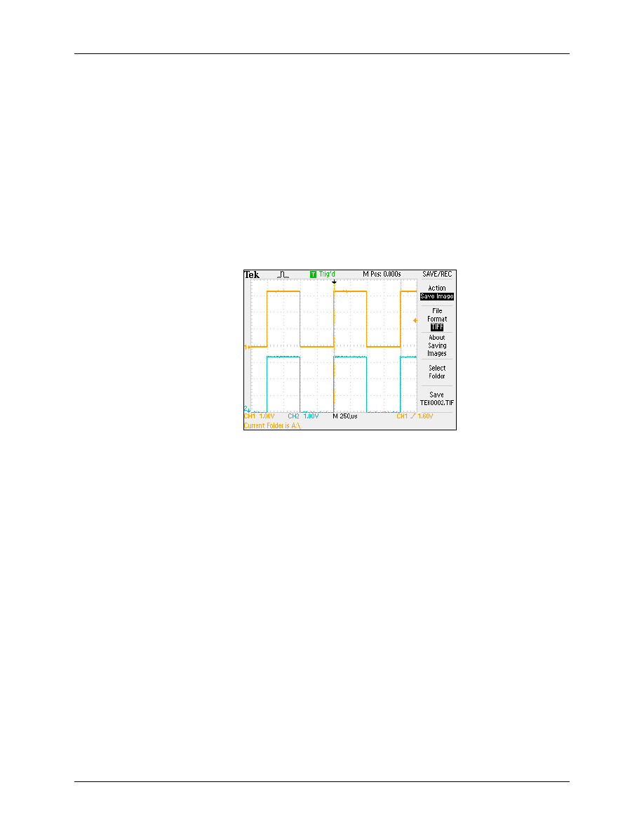
Lab 7_8: Trip Zone protection with TZ6
F2833x - PWM and Capture Units
7 - 57
•
In the register "EPwm1Regs.TZCTL", set TZA and TZB to force ePWM1A and
ePWM1B to zero in case of an active TZ6.
•
In the register "EPwm1Regs.TZSEL", select TZ6 as source for a one shot over current
signal. In the event of an active TZ6 (when we push button PB1), both lines ePWM1A
and ePWM1B will be switched off permanently.
•
Remember that both registers are EALLOW - protected, so please do not forget to open /
close the access to these registers.
Build, Load and Test
5. Build, load and test the modified project. A oscilloscope screenshot of signal ePWM1A and
ePWM1B should show the desired pattern at ePWM1A an ePWM1B:
6. Now push button PB1. Both ePWM1A and ePWM1B should be switched off (0V)
permanently.
One Shot Mode
7. Now let us modify the code in such a way, that an active button PB1 (our trip zone TZ6) will
request a cycle-by-cycle switch off of the two signals ePWM1A and ePWM1B.
•
In the function "Setup_ePWM1()", change register "EPwm1Regs.TZSEL" so that TZ6
will now be the source for a cycle-by-cycle over current signal, and no longer for a one-
shot procedure.
Re-Build, Load and Test
8. Build, load and test the modified project. Please do not forget to reset the DSC before you
perform a new test. This is always a good practice, since the chip will always start from a
known state! Here once more is the required sequence:
•
Debug
Reset CPU
•
Debug
Restart
•
Debug
Go Main

Lab 7_8: Trip Zone protection with TZ6
7 - 58
F2833x - PWM and Capture Units
•
Debug
Run
The scope should again show the pulse sequences at ePWM1A and ePWM1B.
When you push PB1, the signals should fade out to ground and keep this ground voltage, as long
as you keep your finger on PB1 to hold it down. But, when you release PB1, the pulse pattern at
ePWM1A and ePWM1B should reappear again. That's why we this time initialized the F2833x to
resume the PWM operation on a cycle-by-cycle basis!
Add an Interrupt Service
Although we do not have a real power stage system and just the Peripheral Explorer Board, it still
allows us also to perform an exercise with an interrupt service in the event of an over current
situation.
9. At the beginning of "Lab7_8.c", add a prototype for an interrupt service routine:
interrupt void ePWM1_TZ_isr(void);
10. In “main()”, look for the line, in which we change the entry in PieVectTable for TINT0. After
this line, add a new line to replace the entry for EPWM1_TZINT:
PieVectTable.EPWM1_TZINT = &ePWM1_TZ_isr;
11. Interrupt EPWM1_TZINT is wired to PIE - interrupt line INT2 bit 1. We have to enable this
line. In “main()”, search for the line, where we enabled PIEIER1.bit.INTx7. Add a new line
to also enable interrupt 2.1:
PieCtrlRegs.PIEIER2.bit.INTx1 = 1;
12. Change the line "IER |= 1;" so that the two lines INT1 and INT2 are enabled:
IER |= 3;
13. In the function "Setup_ePWM1()", add a line to enable cycle-by-cycle interrupts in register
EPwm1Regs.TZEINT. Include this new instruction in the EALLOW - EDIS block!
14. At the end of "Lab7_8.c", add the definition for function "ePWM1_TZ_isr()". In this function
include the following actions:
•
Clear the two flags "CBC" and "INT" in register "EPwm1Regs.TZCLR" to re-enable TZ6
for the next interrupt service:
EPwm1Regs.TZCLR.bit.CBC = 1;
EPwm1Regs.TZCLR.bit.INT = 1;
Recall that this register is EALLOW - protected!
•
Now, because we "simulate" our over current signal TZ6 using a push button, the
duration of the "over-current" signal depends on how fast we can take our finger off the
button. So what happens, if we push it too long? Answer: TZ6 will trigger a next
interrupt immediately after we return from interrupt function "ePWM1_TZ_isr()".
Remember that we have three different software activities in Lab7_8:

Lab 7_8: Trip Zone protection with TZ6
F2833x - PWM and Capture Units
7 - 59
• “main()” - loop, where we execute the watchdog service #1;
• interrupt service "cpu_timer0_isr()", where we execute the watchdog service #2;
• new interrupt service "ePWM1_TZ_isr()".
Because the interrupt service "cpu_timer0_isr()" has a higher priority than
"ePWM1_TZ_isr()", it will interleave with our finger triggered series of interrupt
requests. The problem is, that the “main()”-loop, and consequently our watchdog service
#1, will be locked out - as long as we keep pushing button PB2.
Solution: push quickly! Or, if you like to push slowly, include the watchdog service #1
into the new interrupt service function "ePWM1_TZ_isr()":
SysCtrlRegs.WDKEY = 0x55;
Remember that this register is also EALLOW - protected!
•
To indicate, that we are executing code from the new interrupt service routine
"ePWM1_TZ_isr", add a line to toggle LED GPIO9:
GpioDataRegs.GPATOGGLE.bit.GPIO9 = 1;
•
To acknowledge that we are done with the interrupt service, in PIE group 2, add:
PieCtrlRegs.PIEACK.all = 2;
15. In the while(1) - loop of “main()”, remove the code for the binary counter at GPIO9, GPIO11,
GPIO34 and GPIO49. Because we will use GPIO9 as an indicator for the new interrupt
service function "ePWM1_TZ_isr()", we cannot use that old block of code any more.
Optionally, you can add a toggle instruction for GPIO11 to the second interrupt service
function "cpu_timer0_isr()".
16. In “main()”, change the line to setup CPU - Timer 0 back to a period of 100 milliseconds:
ConfigCpuTimer(&CpuTimer0,100,100000);
Re-Build, Load and Test
17. Build, load and test the modified project. Please do not forget to reset the device before you
perform a new test. This is always a good practice, since the chip will always start from a
known state! Here's ones more the sequence:
•
Debug
Reset CPU
•
Debug
Restart
•
Debug
Go Main
•
Debug
Run
The scope should again show the pulse sequences at ePWM1A and ePWM1B.
When you push PB1 the signals should fade out to ground and keep this ground voltage, as
long as you keep your finger on PB1 to hold it down. When you release PB1, the pulse pattern
at ePWM1A and ePWM1B should reappear again.
LED LD2 (GPIO11) should toggle with a period of 100 milliseconds.

Lab 7_8: Trip Zone protection with TZ6
7 - 60
F2833x - PWM and Capture Units
Each time you push PB1, LED LD1 (GPIO9) should toggle, as an indication of the execution
of the over current interrupt service routine "ePWM1_TZ_isr()". Please note that button PB1
is a switch with bouncing contacts, so it might request more than one interrupt, when you
press it down.
Of course, in a real-world application, an over-current signal will never be generated by a
push button; we would use a real sensor unit to measure the current in a power stage!
Nevertheless, this exercise with the limited features of the Peripheral Explorer Board includes
all the software features of such a real-world application.
END of Lab7_8
ePWM Interrupt Sources
F2833x - PWM and Capture Units
7 - 61
ePWM Interrupt Sources
7
7
-
-
50
50
ePWM
ePWM
Event
Event
-
-
Trigger Module
Trigger Module
16
16
-
-
Bit
Bit
Time
Time
-
-
Base
Base
Counter
Counter
Compare
Compare
Logic
Logic
Action
Action
Qualifier
Qualifier
Dead
Dead
Band
Band
PWM
PWM
Chopper
Chopper
Shadowed
Compare
Compare
Register
Register
Shadowed
Period
Period
Register
Register
Clock
Clock
Prescaler
Prescaler
Shadowed
Compare
Compare
Register
Register
CMPA . 15 - 0
CMPB . 15 - 0
TBCTR . 15 - 0
TBPRD . 15 - 0
TBCTL . 12 - 7
AQCTLB . 11 - 0
AQCTLA . 11 - 0
DBCTL . 4 - 0
PCCTL . 10 - 0
SYSCLKOUT
SYSCLKOUT
EPWMxSYNCI
EPWMxSYNCI
EPWMxSYNCO
EPWMxSYNCO
TBCLK
TBCLK
Trip
Trip
Zone
Zone
TZSEL . 15 - 0
EPWMxA
EPWMxA
EPWMxB
EPWMxB
TZy
TZy
We still have left one module of the ePWM unit: the event trigger sub module. It monitors
various event conditions, such as
Counter value TBCTR = zero
Counter value TBCTR = TBPRD
Counter value TBCTR = CMPA
Counter value TBCTR = CMPB
and can be configured to prescale these events before issuing an Interrupt request or an ADC start
of conversion. The event-trigger prescaling logic can issue Interrupt requests and ADC start of
conversion at:
Every event
Every second event
Every third event
The next slide is an example for symmetrical PWM operation mode and shows available point of
actions for interrupt service requests or to start an analogue to digital conversion:
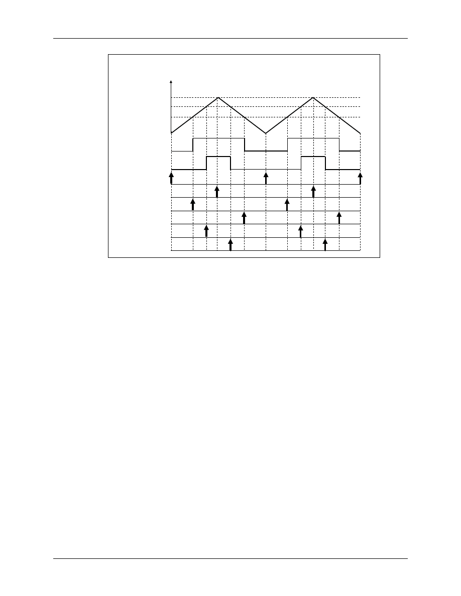
ePWM Interrupt Sources
7 - 62
F2833x - PWM and Capture Units
7
7
-
-
51
51
ePWM
ePWM
Event
Event
-
-
Trigger Interrupts and SOC
Trigger Interrupts and SOC
TBCTR
TBCTR
TBPRD
TBPRD
.
.
.
.
.
.
.
.
.
.
.
.
.
.
.
.
EPWMA
EPWMA
EPWMB
EPWMB
CMPB
CMPB
CMPA
CMPA
CTR = 0
CTR = 0
CTR = PRD
CTR = PRD
CTRU = CMPA
CTRU = CMPA
CTRD = CMPA
CTRD = CMPA
CTRU = CMPB
CTRU = CMPB
CTRD = CMPB
CTRD = CMPB
The Event-Trigger- Sub module is initialized by a set of registers:
ETSEL
-
This register selects which of the possible events will trigger an
interrupt or start an ADC conversion
ETPS
-
This register programs the event prescaling options mentioned
above.
ETFLG
-
Register with flag bits to indicate the status of the selected and
prescaled events.
ETCLR
-
These bits allow you to clear the flag bits in the ETFLG register
via software.
ETFRC
-
These bits allow software forcing of an event. Useful for
debugging or s/w intervention.
We will use one of the interrupts of the event trigger module in the next lab exercise Lab7_9 to
request a change of the pulse width on a cycle by cycle base (or "on the fly") to generate a sine
wave modulated signal at ePWM1A.
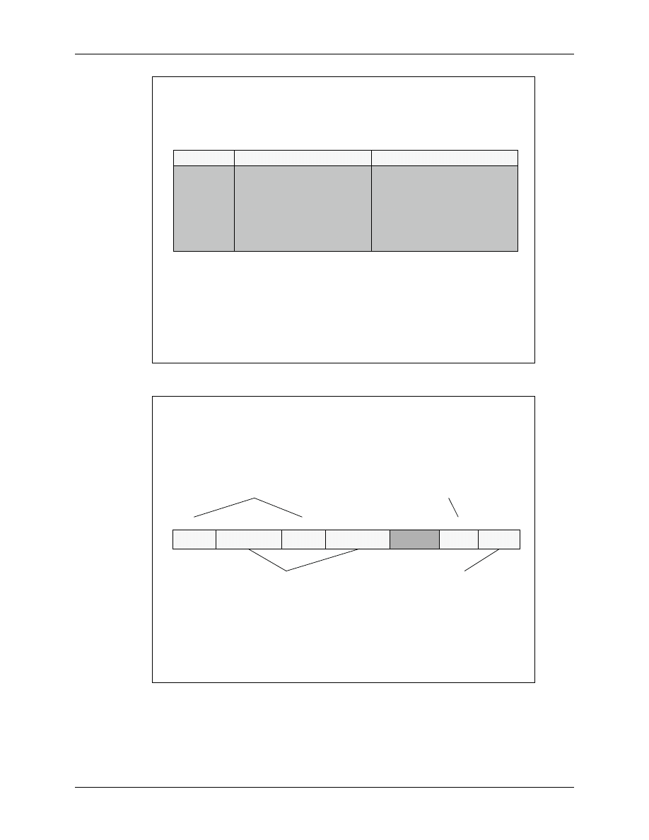
ePWM Interrupt Sources
F2833x - PWM and Capture Units
7 - 63
7
7
-
-
52
52
ePWM
ePWM
Event
Event
-
-
Trigger Module Registers
Trigger Module Registers
Name
Name
Description
Description
Structure
Structure
ETSEL
ETSEL
Event
Event
-
-
Trigger Selection
Trigger Selection
EPwm
EPwmx
Regs.ETSEL.all
Regs.ETSEL.all
=
=
ETPS
ETPS
Event
Event
-
-
Trigger Pre
Trigger Pre
-
-
Scale
Scale
EPwm
EPwmx
Regs.ETPS.all
Regs.ETPS.all
=
=
ETFLG
ETFLG
Event
Event
-
-
Trigger Flag
Trigger Flag
EPwm
EPwmx
Regs.ETFLG.all
Regs.ETFLG.all
=
=
ETCLR
ETCLR
Event
Event
-
-
Trigger Clear
Trigger Clear
EPwm
EPwmx
Regs.ETCLR.all
Regs.ETCLR.all
=
=
ETFRC
ETFRC
Event
Event
-
-
Trigger Force
Trigger Force
EPwm
EPwmx
Regs.ETFRC.all
Regs.ETFRC.all
=
=
7
7
-
-
53
53
ePWM
ePWM
Event
Event
-
-
Trigger Selection Register
Trigger Selection Register
EPwm
EPwmx
Regs.ETSEL
Regs.ETSEL
15
15
11
11
7
7
-
-
4
4
2
2
-
-
0
0
INTEN
INTEN
INTSEL
INTSEL
reserved
3
3
SOCBSEL
SOCBSEL
SOCASEL
SOCASEL
SOCAEN
SOCAEN
SOCBEN
SOCBEN
10
10
-
-
8
8
14
14
-
-
12
12
Enable SOCB / A
Enable SOCB / A
0 = disable
0 = disable
1 = enable
1 = enable
EPWMxSOCB
EPWMxSOCB
/ A Select
/ A Select
000 = reserved
000 = reserved
001 = CTR = 0
001 = CTR = 0
010 = CTR = PRD
010 = CTR = PRD
011 = reserved
011 = reserved
100 = CTRU = CMPA
100 = CTRU = CMPA
101 = CTRD = CMPA
101 = CTRD = CMPA
110 = CTRU = CMPB
110 = CTRU = CMPB
111 = CTRD = CMPB
111 = CTRD = CMPB
Enable
Enable
EPWMxINT
EPWMxINT
0 = disable
0 = disable
1 = enable
1 = enable
EPWMxINT
EPWMxINT
Select
Select
000 = reserved
000 = reserved
001 = CTR = 0
001 = CTR = 0
010 = CTR = PRD
010 = CTR = PRD
011 = reserved
011 = reserved
100 = CTRU = CMPA
100 = CTRU = CMPA
101 = CTRD = CMPA
101 = CTRD = CMPA
110 = CTRU = CMPB
110 = CTRU = CMPB
111 = CTRD = CMPB
111 = CTRD = CMPB
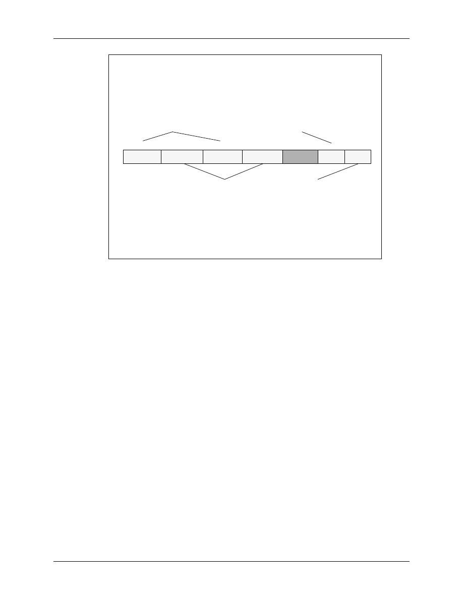
ePWM Interrupt Sources
7 - 64
F2833x - PWM and Capture Units
7
7
-
-
54
54
ePWM
ePWM
Event
Event
-
-
Trigger
Trigger
Prescale
Prescale
Register
Register
EPwm
EPwmx
Regs.ETPS
Regs.ETPS
15
15
-
-
14
14
11
11
-
-
10
10
7
7
-
-
4
4
1
1
-
-
0
0
INTCNT
INTCNT
INTPRD
INTPRD
reserved
2
2
-
-
3
3
SOCBPRD
SOCBPRD
SOCAPRD
SOCAPRD
SOCACNT
SOCACNT
SOCBCNT
SOCBCNT
9
9
-
-
8
8
13
13
-
-
12
12
EPWMxSOCB
EPWMxSOCB
/ A Counter
/ A Counter
(number of events have occurred)
00 = no events
00 = no events
01 = 1 event
01 = 1 event
10 = 2 events
10 = 2 events
11 = 3 events
11 = 3 events
EPWMxSOCB
EPWMxSOCB
/ A Period
/ A Period
(number of events before SOC)
00 = disabled
00 = disabled
01 = SOC on first event
01 = SOC on first event
10 = SOC on second event
10 = SOC on second event
11 = SOC on third event
11 = SOC on third event
EPWMxINT
EPWMxINT
Counter
Counter
(number of events have occurred)
00 = no events
00 = no events
01 = 1 event
01 = 1 event
10 = 2 events
10 = 2 events
11 = 3 events
11 = 3 events
EPWMxINT
EPWMxINT
Period
Period
(number of events before INT)
00 = disabled
00 = disabled
01 = INT on first event
01 = INT on first event
10 = INT on second event
10 = INT on second event
11 = INT on third event
11 = INT on third event
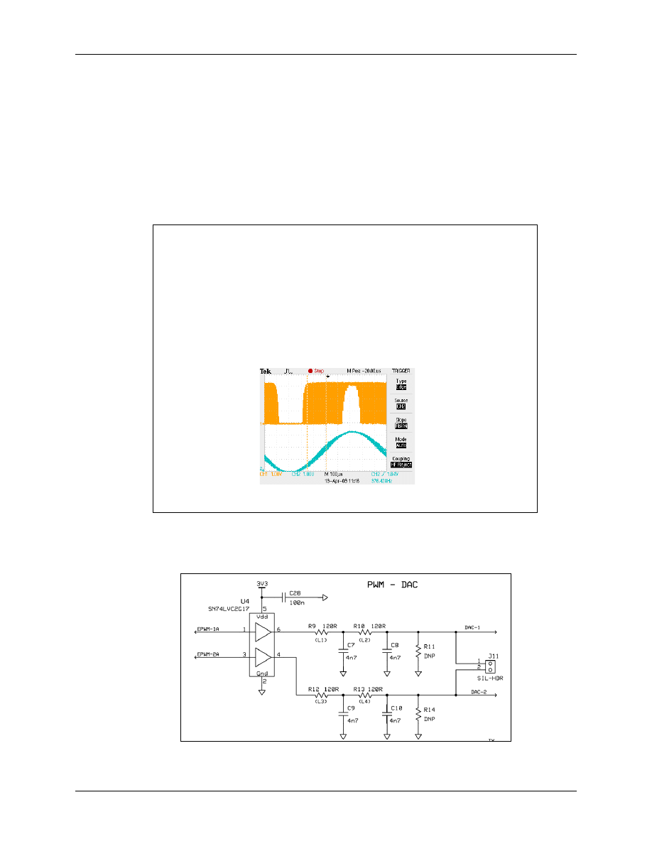
Lab7_9: ePWM Sine Wave Modulation
F2833x - PWM and Capture Units
7 - 65
Lab7_9: ePWM Sine Wave Modulation
Objective
The F28335ControlCARD is used in combination with the Peripheral Explorer Board to output a
sine wave signal at ePWM1A. Channel ePWM1A is set up in standard 16-bit resolution. The
generated signal is connected to a second order low pass filter with a cut-off frequency of 105
kHz. The filter output signal can be monitored at header J11-1 (“DAC-1”) of the Peripheral
Explorer Board.
7
7
-
-
55
55
Lab 7_9: Sine Wave PWM signal at ePWM1A
Lab 7_9: Sine Wave PWM signal at ePWM1A
• Generate a sine wave modulated pulse sequence at
ePWM1A
• ePWM1A carrier frequency is 500 KHz
• Sine wave frequency is 976 Hz
Objective:
Objective:
Channel ePWM1A is set up for a 500 kHz PWM frequency, ePWM1 compare down event
triggers an interrupt service routine (ISR), according to the frequency the trigger appears every
2.000 ns.
Lab7_9: ePWM Sine Wave Modulation
7 - 66
F2833x - PWM and Capture Units
The ISR with a code execution time of 630ns takes advantage of the Boot-ROM sine wave
lookup-table to calculate the next compare value for the next ePWM1A period. The lookup-table
consists of 512 values in I2Q30-format and is located at address 0x3FE000. Every ISR call is
used to read the next entry of this table, thus a full period of the resulting sine wave takes 512 *
2000 ns = 1024 µs. The synthesized sine wave signal has a frequency of 1/1024µs = 976 Hz. Due
to the type of look-up values in I2Q30-format, functions of a library called “IQmath” are used to
calculate the next value for the duty cycle.
Although we have not discussed the background of fixed-point binary mathematics and especially
of Texas Instruments IQMath yet, we will use this library in a 'black box' method. We will
resume the discussion of this mathematical approach in a later chapter of this teaching course.
Procedure
Install IQMath
If not already installed on your PC, you will have to install the IQMath library now. The standard
installation path is "C:\tidcs\c28\IQmath":
If this library isn't available on your PC, you will have to install it first. If you are in a classroom
and you do not have administrator installation rights, ask your teacher for assistance. You can
find the installation file under number "sprc087.zip" in the utility part of this CD-ROM or at the
Texas Instruments Website (www.ti.com).
Open Project File
1. In project "Lab7" open the file “Lab7_8.c” and save it as “Lab7_9.c”
2. Add “Lab7_9.c” to the project and exclude “Lab7_8.c” from build. Use a right mouse click
on file “Lab7_8.c”, select “File Specific Options”; in category “General” enable “Exclude
from Build”.
3. Change the Build options.

Lab7_9: ePWM Sine Wave Modulation
F2833x - PWM and Capture Units
7 - 67
We have to extend the preprocessors include search path. Open Project Build Options and go
to the preprocessor category. The "Include Search Path" already has two entries. Do not
delete these entries! Instead, at the end of this line add a semicolon and a third entry:
; C:\tidcs\c28\IQmath\v15\include
Close the Build options menu with <OK>
4. Add IQmath library to your project. Add:
C:\tidcs\c28\IQmath\v15\lib\IQmath_fpu32.lib
5. At the beginning of "Lab7_9.c" include the header file for IQmath:
#include "IQmathLib.h"
Also at the beginning of "Lab7_9.c", add a new global variable "sine_table[512]" of data type
"_iq30" to "Lab7_9.c":
#pragma DATA_SECTION(sine_table, "IQmathTables");
_iq30 sine_table[512];
The pragma statement is a directive for the compiler to generate a new data section for
"sine_table". The linker command file "28335_RAM_lnk.cmd", which is already part of our
project, will connect the section "IQmathTables" to physical address 0x3FE000, which is
where our lookup table is stored in ROM.
6. In "Lab7_9.c" remove everything that is related to CpuTimer0, including external function
prototypes, the call to functions "InitCpuTimers()", "ConfigCpuTimer()" and Interrupt
Service Routine "cpu_timer0_isr()", including its prototype and definition. In the while(1)
loop of main, also remove all instruction related to variable "CpuTimer0.InterruptCount".
Also remove everything that is related to variable "counter". We do not need this variable any
more.
7. Also at the beginning of "Lab7_9.c", replace the function prototype of ISR
"ePWM1_TZ_isr()" by a new interrupt service function prototype:
interrupt void ePWM1A_compare_isr(void);
8. In “main()”, remove the entry instruction to write into "PieVectTable.EPWM1_TZINT" and
add a new instruction:
PieVectTable.EPWM1_INT = &ePWM1A_compare_isr;
PWM1 interrupts are connected to PIE group 3, bit 1. Therefore change the line to enable PIE
interrupts into:
PieCtrlRegs.PIEIER3.bit.INTx1 = 1;
Change register IER to allow interrupts at line 3:
IER |= 4;
9. In the while(1) - loop of main keep just the instruction to service the watchdog instruction #1
(value 0x55) to register WDKEY. Remember that the register WDKEY is EALLOW
protected!

Lab7_9: ePWM Sine Wave Modulation
7 - 68
F2833x - PWM and Capture Units
10. Next, in the function "Gpio_select()", just keep ePWM1A as PWM output signal. Remove
the instructions to enable lines ePWM1B and TZ6.
11. In the function "Setup_ePWM1()", change the period of ePWM1 to 500 kHz. In up/down
mode the value for TBPRD is calculated by:
HSPCLKDIV
CLKDIV
f
f
TBPRD
PWM
SYSCLKOUT
*
*
2
1 ∗
=
with CLKDIV and HSPCLKDIV both set to "divide by 1" and f
SYSCLKOUT
= 150MHz,
TBPRD should be initialized to 150.
12. Then in the function "Setup_ePWM1()", remove the initialization lines for registers CMPB
an AQCTLB, since we will not generate a signal at ePWM1B.
13. At the end of the function "Setup_ePWM1()", remove the code to initialize the trip zone unit,
including all instructions for registers TZCTL, TZSEL and TZEINT.
14. At the end of the function "Setup_ePWM1()", add code to initialize the Event Trigger
module. In the register "ETSEL", enable bit "INTEN" and set the bit field "INTSEL" to select
an interrupt request, if CTRD = CMPA (counter down matches CMPA). In the register
"ETPS", set bit field "INTPRD" to request an interrupt on first event.
15. At the end of "Lab7_9.c" add the definition of function "ePWM1A_compare_isr()":
interrupt void ePWM1A_compare_isr(void)
{
First define a static variable "index" and initialize it to zero. This variable will be used as an
index into lookup-table "sine_table[512]:
static unsigned int index = 0;
Next we have to service the second half of the watchdog - key sequence to register WDKEY
(value 0xAA). Remember that this register is EALLOW protected!
Now we have to calculate a new value for register CMPA. Here is the line:
EPwm1Regs.CMPA.half.CMPA =
EPwm1Regs.TBPRD -_IQsat(
_IQ30mpy((sine_table[index]+_IQ30(0.9999))/2, EPwm1Regs.TBPRD),
EPwm1Regs.TBPRD,0);
Confusing, isn't it?
Here is an attempt to explain it, should you be interested in the details:
Recall, the difference between TBPRD and CMPA defines the pulse width of the
PWM signal. The bigger the difference, the bigger the pulse. It means that we have to
subtract a percentage value from TBPRD to define the next pulse width and store this
percent value in CMPA.
To find that next value to be subtracted from TBPRD we have to access the sine
table. Variable "index" points to this table, which consists of 512 entries for a unit
circle of 360 degrees. The value taken from this table is in I2Q30-Format and

Lab7_9: ePWM Sine Wave Modulation
F2833x - PWM and Capture Units
7 - 69
between 0 for sin(0), 1 for sin(90°), 0 for sin(180°), -1 for sin(270°) and again 0 for
sin(360°).
So, we read a number between +1 and -1, which corresponds to the current amplitude
of the sine. However, we cannot use a negative number for the calculation of a result
between 0 and 100% of TBPRD. What we do is we add an offset of +1 in the form of
an IQ-number (_IQ30(0.9999)) to obtain numbers between 0 and +2. Next we divide
the result by 2 to scale it into a range between 0 and 1 (or 0% and 100%).
Now we multiply this relative number (0 to 1) by TBPRD with a call of function
"_IQ30mpy( )" . If TBPRD has been set to 100, the result will be a number between 0
and 100.
The function "_IQsat()" is a saturation function that will limit the first parameter (our
result) between maximum (parameter 2, TBPRD) and minimum (parameter 3, zero).
To call this function is just a precaution to avoid any calculation overflows, which
could result in catastrophic output signals, where a large positive number suddenly
becomes a large negative number.
After this calculation, still inside "ePWM1A_compare_isr()", we have to increment variable
"index" and to reset it, if we are at the end of the sine_table:
index +=1;
if( index > 511) index = 0;
Finally, we have to clear the interrupt flags of the event trigger module and the PIE-unit:
EPwm1Regs.ETCLR.bit.INT = 1;
PieCtrlRegs.PIEACK.all = 4;
Close function "ePWM1A_compare_isr()" with a closing curly brace ( }).
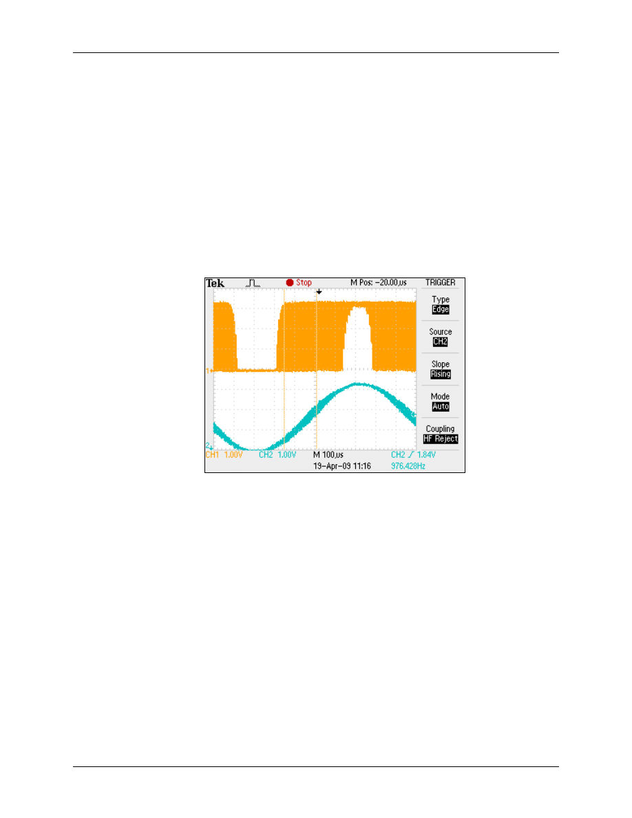
Lab7_9: ePWM Sine Wave Modulation
7 - 70
F2833x - PWM and Capture Units
Build, Load and Test
16. Build, load and test the modified project. Please do not forget to reset the DSC before you
perform a new test. This is always a good practice, since the chip will always start from a
known state! Here's the sequence:
•
Debug
Reset CPU
•
Debug
Restart
•
Debug
Go Main
•
Debug
Run
17. A scope should show the 500 kHz-pulse sequence at ePWM1A (Peripheral Explorer Board
Jumper J6-1) and a sine wave signal of 976 Hz at DAC1 (Peripheral Explorer Board Jumper
J11-1).
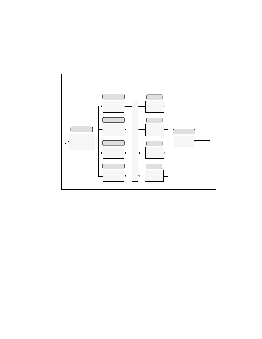
eCAP Capture Module
F2833x - PWM and Capture Units
7 - 71
eCAP Capture Module
The enhanced Capture (eCAP) module provides measurement units, which are useful for accurate
time stamps of external events, such as rising or falling edges of digital signals.
Capture Operating Mode
7
7
-
-
56
56
eCAP
eCAP
Block Diagram
Block Diagram
–
–
Capture Mode
Capture Mode
32
32
-
-
Bit
Bit
Time
Time
-
-
Stamp
Stamp
Counter
Counter
Capture 1
Capture 1
Register
Register
Event
Event
Prescale
Prescale
Polarity
Polarity
Select 1
Select 1
Polarity
Polarity
Select 2
Select 2
Polarity
Polarity
Select 3
Select 3
Polarity
Polarity
Select 4
Select 4
Capture 2
Capture 2
Register
Register
Capture 3
Capture 3
Register
Register
Capture 4
Capture 4
Register
Register
E
v
e
n
t L
o
g
ic
E
v
e
n
t L
o
g
ic
ECAPx
ECAPx
pin
pin
SYSCLKOUT
SYSCLKOUT
TSCTR . 31 - 0
CAP1 . 31 - 0
CAP2 . 31 - 0
CAP3 . 31 - 0
CAP4 . 31 - 0
ECCTL . 13 - 9
ECCTL . 0
ECCTL . 2
ECCTL . 4
ECCTL . 6
CAP1POL
CAP1POL
CAP2POL
CAP2POL
CAP3POL
CAP3POL
CAP4POL
CAP4POL
PRESCALE
PRESCALE
The capture units allow time-based logging of external logic level signal transitions on the
capture input pins.
Devices in the F2833x family have four independent capture units; one of them is shown in Slide
7-56 above. Each capture unit is associated with a capture input pin. An event prescaler can be
initialized to reduce the input frequency. Four polarity select bit fields define rising or falling
edges as the trigger events for capture events 1 to 4. The measurement time-base is derived from
the frequency SYSCLKOUT, in the case of the F28335ControlCard, this is 100 MHz. This signal
will increment a 32-bit Time-Stamp Counter. In the event of a capture trigger signal the current
value of this counter is captured and stored in the corresponding capture register.
Multiple identical eCAP modules can be contained in a 2833x system as shown in Slide 7-56.
The number of modules is device-dependent and is based on target application needs.
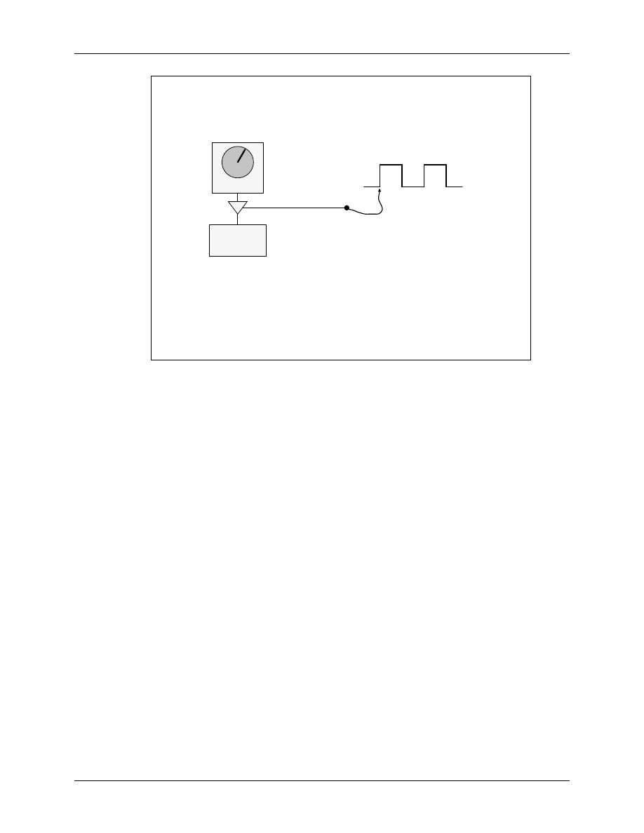
eCAP Capture Module
7 - 72
F2833x - PWM and Capture Units
7
7
-
-
57
57
Capture Units (
Capture Units (
eCAP
eCAP
)
)
The
The
eCAP
eCAP
module timestamps transitions on a
module timestamps transitions on a
capture input pin
capture input pin
Timer
Timestamp
Values
Trigger
pin
Typical uses for the Capture Units are:
• Period and duty cycle measurements of pulse train signals
• Low speed measurement of a rotating machinery (e.g., toothed sprockets sensed via Hall
sensors). A potential advantage for low speed estimation is given when we use “time
capture” (32-bit resolution) instead of position pulse counting, which has a poor
resolution at slow operating speeds.
• Elapsed time measurements between position sensor pulses.
• Decoding current or voltage amplitude derived from duty cycle encoded current/voltage
sensors
Additionally, if the capture operation is not used in an application, an ePWM channel can be used
as another single ended ePWM - output channel, with 32-bit resolution for frequency and duty
cycle register setup. Since this operation mode is not the primary purpose of this unit, it is called
"Auxiliary PWM" mode.
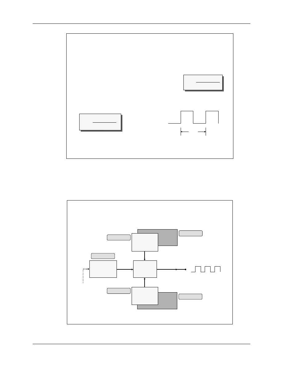
eCAP Capture Module
F2833x - PWM and Capture Units
7 - 73
7
7
-
-
58
58
Some Uses for the Capture Units
Some Uses for the Capture Units
Problem: At low speeds, calculation of speed
based on a measured position change at
fixed time intervals produces large estimate
errors
Alternative: Estimate the speed using a measured time interval
at fixed position intervals
Signal from one
quadrature
encoder channel
Low speed velocity estimation from incr. encoder:
Measure the time width of a pulse
v
k
≈
∆x
t
k
- t
k-1
v
k
≈
∆t
x
k
- x
k-1
∆x
Auxiliary PWM generation
Auxilliary PWM Operating Mode
As a second operating mode of a capture unit, auxiliary PWM mode can be used. In this case a
single ended output PWM signal can be generated. Register CAP1 features as period register and
register CAP2 as compare register.
7
7
-
-
59
59
eCAP
eCAP
Block Diagram
Block Diagram
–
–
APWM Mode
APWM Mode
32
32
-
-
Bit
Bit
Time
Time
-
-
Stamp
Stamp
Counter
Counter
Period
Period
Register
Register
(CAP3)
(CAP3)
Period
Period
Register
Register
(CAP1)
(CAP1)
Compare
Compare
Register
Register
(CAP4)
(CAP4)
Compare
Compare
Register
Register
(CAP2)
(CAP2)
PWM
PWM
Compare
Compare
Logic
Logic
ECAP
ECAP
pin
pin
Shadowed
Shadowed
SYSCLKOUT
SYSCLKOUT
TSCTR . 31 - 0
CAP1 . 31 - 0
CAP2 . 31 - 0
CAP3 . 31 - 0
CAP4 . 31 - 0
immediate
immediate
mode
mode
shadow
shadow
mode
mode
shadow
shadow
mode
mode
immediate
immediate
mode
mode
Capture Units Registers
7 - 74
F2833x - PWM and Capture Units
Capture Units Registers
Each of the four capture units is controlled by a set of individual registers.
7
7
-
-
60
60
eCAP
eCAP
Module Registers
Module Registers
Name
Name
Description
Description
Structure
Structure
ECCTL1 Capture Control 1
ECCTL1 Capture Control 1
ECap
ECapx
Regs.ECCTL1.all =
Regs.ECCTL1.all =
ECCTL2 Capture Control 2
ECCTL2 Capture Control 2
ECap
ECapx
Regs.ECCTL2.all =
Regs.ECCTL2.all =
TSCTR
TSCTR
Time
Time
-
-
Stamp Counter
Stamp Counter
ECap
ECapx
Regs.TSCTR
Regs.TSCTR
=
=
CTRPHS Counter Phase Offset
CTRPHS Counter Phase Offset
ECap
ECapx
Regs.CTRPHS
Regs.CTRPHS
=
=
CAP1
CAP1
Capture 1
Capture 1
ECap
ECapx
Regs.CAP1 =
Regs.CAP1 =
CAP2
CAP2
Capture 2
Capture 2
ECap
ECapx
Regs.CAP2 =
Regs.CAP2 =
CAP3
CAP3
Capture 3
Capture 3
ECap
ECapx
Regs.CAP3 =
Regs.CAP3 =
CAP4
CAP4
Capture 4
Capture 4
ECap
ECapx
Regs.CAP4 =
Regs.CAP4 =
ECEINT Enable Interrupt
ECEINT Enable Interrupt
ECap
ECapx
Regs.ECEINT.all
Regs.ECEINT.all
=
=
ECFLG
ECFLG
Interrupt Flag
Interrupt Flag
ECap
ECapx
Regs.ECFLG.all
Regs.ECFLG.all
=
=
ECCLR
ECCLR
Interrupt Clear
Interrupt Clear
ECap
ECapx
Regs.ECCLR.all
Regs.ECCLR.all
=
=
ECFRC
ECFRC
Interrupt Force
Interrupt Force
ECap
ECapx
Regs.ECFRC.all
Regs.ECFRC.all
=
=
eCAP Control Register 1
7
7
-
-
61
61
eCAP
eCAP
Control Register 1
Control Register 1
ECap
ECapx
Regs.ECCTL1
Regs.ECCTL1
CAPLDEN
CAPLDEN
FREE_SOFT
FREE_SOFT
PRESCALE
PRESCALE
15
15
-
-
14
14
13
13
-
-
9
9
8
8
Upper Register:
Upper Register:
Emulation Control
Emulation Control
00 = TSCTR stops immediately
00 = TSCTR stops immediately
01 = TSCTR runs until equals 0
01 = TSCTR runs until equals 0
1X = free run (do not stop)
1X = free run (do not stop)
Event Filter
Event Filter
Prescale
Prescale
Counter
Counter
00000 = divide by 1 (bypass)
00000 = divide by 1 (bypass)
00001 = divide by 2
00001 = divide by 2
00010 = divide by 4
00010 = divide by 4
00011 = divide by 6
00011 = divide by 6
00100 = divide by 8
00100 = divide by 8
11110 = divide by 60
11110 = divide by 60
11111 = divide by 62
11111 = divide by 62
CAP1
CAP1
–
–
4 Load
4 Load
on Capture Event
on Capture Event
0 = disable
0 = disable
1 = enable
1 = enable

Capture Units Registers
F2833x - PWM and Capture Units
7 - 75
ECCTL1 [15-14] specify the interaction between the DSC and the JTAG emulation unit. If a
running code hits a breakpoint, these two bits define how the capture unit behaves in this
situation.
The prescaler counter in ECCTL1 [13-9] is used as an input filter of the capture signal. If set to
"00001", every other edge is used to trigger the capture unit.
ECCTL [8] is the global enable switch for the particular capture unit.
ECCTL1 [6, 4, 2, 0] define rising (0) or falling (1) edge as trigger signal for capture event 1 to 4
ECCTL1 [7, 5, 3, 1] specify absolute (0) or relative (1) time stamp mode. Absolute mode will
never clear the timestamp - counter, after the capture unit has been started. Relative mode will
clear the timestamp - counter simultaneously with the trigger event. For example, if bits 0 and 1
are initialized to 1, the first falling edge after enabling the capture unit will zero the timestamp-
counter.
7
7
-
-
62
62
eCAP
eCAP
Control Register 1
Control Register 1
ECap
ECapx
Regs.ECCTL1
Regs.ECCTL1
Lower Register:
Lower Register:
CTRRST4
CTRRST4
CAP4POL
CAP4POL
7
7
3
3
0
0
2
2
CTRRST3
CTRRST3
CAP3POL
CAP3POL
CTRRST2
CTRRST2
CAP2POL
CAP2POL
CTRRST1
CTRRST1
CAP1POL
CAP1POL
1
1
4
4
5
5
6
6
Counter Reset on Capture Event
Counter Reset on Capture Event
0 = no reset
0 = no reset
(absolute time stamp mode)
1 = reset after capture
1 = reset after capture
(difference mode)
Capture Event Polarity
Capture Event Polarity
0 = trigger on rising edge
0 = trigger on rising edge
1 = trigger on falling edge
1 = trigger on falling edge
Capture Units Registers
7 - 76
F2833x - PWM and Capture Units
eCAP Control Register 2
ECCTL2 [10] defines the shape of an ePWM - output signal in auxiliary PWM operation mode
to be active high (0) or active low (1). In capture operating mode, this bit is don't care.
ECTTL2 [9] selects either capture operating mode (0) or auxiliary PWM mode (1).
7
7
-
-
63
63
eCAP
eCAP
Control Register 2
Control Register 2
ECap
ECapx
Regs.ECCTL2
Regs.ECCTL2
Upper Register:
Upper Register:
SWSYNC
SWSYNC
APWMPOL
APWMPOL
CAP_APWM
CAP_APWM
10
10
8
8
15
15
-
-
11
11
reserved
9
9
APWM Output Polarity
APWM Output Polarity
(valid only in APWM mode)
0 = active high output
0 = active high output
1 = active low output
1 = active low output
Capture / APWM mode
Capture / APWM mode
0 = capture mode
0 = capture mode
1 = APWM mode
1 = APWM mode
Software Force
Software Force
Counter Synchronization
Counter Synchronization
0 = no effect
0 = no effect
1 = TSCTR load of current
1 = TSCTR load of current
module
module
and other modules
and other modules
if SYNCO_SEL bits = 00
if SYNCO_SEL bits = 00
ECTTL2 [8] can be used in APWM-Mode to synchronize different capture units with each other.
In case of an active sync input signal, register TSCTR is loaded with a start value.
Capture Units Registers
F2833x - PWM and Capture Units
7 - 77
7
7
-
-
64
64
eCAP
eCAP
Control Register 2
Control Register 2
ECap
ECapx
Regs.ECCTL2
Regs.ECCTL2
Lower Register:
Lower Register:
SYNCO_SEL
SYNCO_SEL
SYNCI_EN
SYNCI_EN
7
7
-
-
6
6
3
3
0
0
2
2
-
-
1
1
TSCTRSTOP
TSCTRSTOP
REARM
REARM
STOP_WRAP
STOP_WRAP
CONT_ONESHT
CONT_ONESHT
4
4
5
5
Sync
Sync
-
-
Out Select
Out Select
00 = sync
00 = sync
-
-
in to sync
in to sync
-
-
out
out
01 = CTR = PRD event
01 = CTR = PRD event
generates sync
generates sync
-
-
out
out
1X = disable
1X = disable
Counter Sync
Counter Sync
-
-
In
In
0 = disable
0 = disable
1 = enable
1 = enable
Time Stamp
Time Stamp
Counter Stop
Counter Stop
0 = stop
0 = stop
1 = run
1 = run
Re
Re
-
-
arm
arm
(capture mode only)
0 = no effect
0 = no effect
1 = arm sequence
1 = arm sequence
Stop Value for One
Stop Value for One
-
-
Shot Mode/
Shot Mode/
Wrap Value for Continuous Mode
Wrap Value for Continuous Mode
(capture mode only)
00 = stop/wrap after capture event 1
00 = stop/wrap after capture event 1
01 = stop/wrap after capture event 2
01 = stop/wrap after capture event 2
10 = stop/wrap after capture event 3
10 = stop/wrap after capture event 3
11 = stop/wrap after capture event 4
11 = stop/wrap after capture event 4
Continuous/One
Continuous/One
-
-
Shot
Shot
(capture mode only)
0 = continuous mode
0 = continuous mode
1 = one
1 = one
-
-
shot mode
shot mode
ECTTL2 [7-6] are used to specify the source of the sync output signal (to achieve synchronized
APWM channels). The code 00 will directly drive a sync input signal to the sync output. Code 01
will sent a sync output signal to other capture channels, if TBCTR = TBPRD.
ECTTL2 [5] allows the APWM sync input feature.
ECTTL2 [4] is the master switch to enable the capture counter unit.
ECTTL2 [3-0]: The continuous/one-shot block controls the start/stop and reset (zero) functions
of a Modulo 4 event counter via a mono-shot type of action that can be triggered by the stop-
value comparator and re-armed via software control.
One shot mode:
Once armed, the eCAP module waits for 1 to 4 (defined by the stop-value) capture events
before freezing both the Modulo 4 event counter and the contents of registers CAP1 to 4
(i.e. time-stamps). Re-arming prepares the eCAP module for another capture sequence.
Also re-arming clears the Modulo 4 counter to zero and permits loading of CAP1-4
registers again, providing that the CAPLDEN bit is set.
Continuous Mode:
In continuous mode, the Modulo 4 event counter continues to run (0->1->2->3->0, the
one-shot action is ignored, and capture values continue to be written to capture result
registers CAP1 - x in a circular buffer sequence. The wrap around value will limit
number x to the pre-selected result register.
eCAP Interrupt Enable Register
Interrupts can be requested based on internal events of the capture or APWM module.
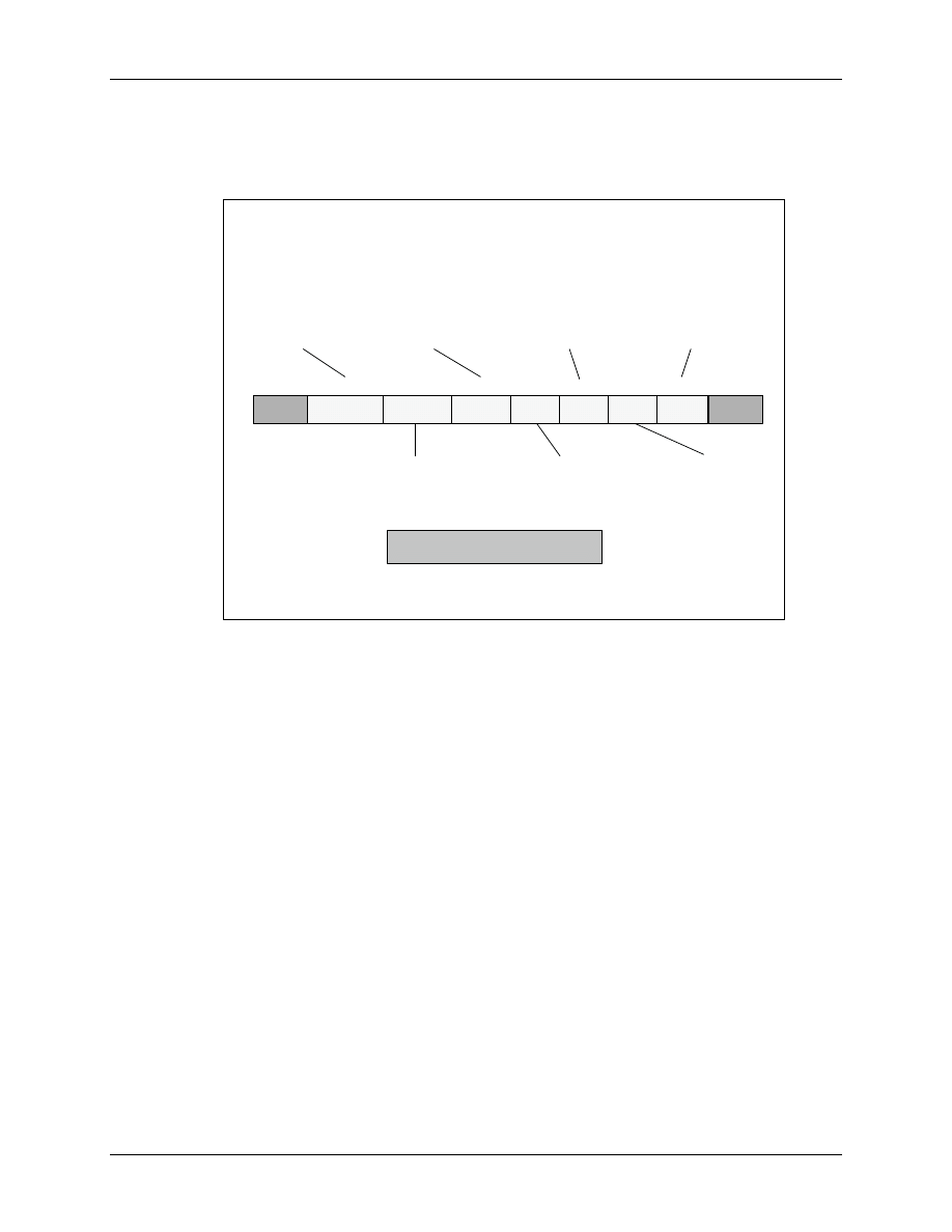
Capture Units Registers
7 - 78
F2833x - PWM and Capture Units
ECEINT [4-1] will enable an interrupt request with capture event 1 to 4.
ECEINT [5] can be used to request an ISR in case of an overflow of the 32-bit register TBCTR.
It is important to note such an overflow when results will be subtracted in a later calculation.
7
7
-
-
65
65
eCAP
eCAP
Interrupt Enable Register
Interrupt Enable Register
ECap
ECapx
Regs.ECEINT
Regs.ECEINT
CTR=CMP
CTR=CMP
CTR=PRD
CTR=PRD
7
7
3
3
0
0
2
2
CTROVF
CTROVF
CEVT4
CEVT4
CEVT3
CEVT3
CEVT2
CEVT2
CEVT1
CEVT1
1
1
4
4
5
5
6
6
reserved
15
15
-
-
8
8
reserved
0 = disable as interrupt source
0 = disable as interrupt source
1 = enable as interrupt source
1 = enable as interrupt source
CTR = CMP
CTR = CMP
Interrupt Enable
Interrupt Enable
CTR = PRD
CTR = PRD
Interrupt Enable
Interrupt Enable
CTR = Overflow
CTR = Overflow
Interrupt Enable
Interrupt Enable
Capture Event 3
Capture Event 3
Interrupt Enable
Interrupt Enable
Capture Event 1
Capture Event 1
Interrupt Enable
Interrupt Enable
Capture Event 4
Capture Event 4
Interrupt Enable
Interrupt Enable
Capture Event 2
Capture Event 2
Interrupt Enable
Interrupt Enable
ECEINT [7, 6] are interrupt enable bits used in APWM mode. If TBCTR matches either register
CMP or PRD, a corresponding interrupt service routine can be requested.

Lab7_10: ePWM1A 1 kHz signal captured by eCAP1
F2833x - PWM and Capture Units
7 - 79
Lab7_10: ePWM1A 1 kHz signal captured by eCAP1
Objective
The F28335ControlCARD is used in combination with the Peripheral Explorer Board to output a
1 kHz square wave signal with a duty cycle of 50% at ePWM1A. We will use unit eCAP1 to
measure period and duty cycle of this signal.
Note: for this exercise you will have to connect header J6-1 (ePWM1A) to header J10-1
(eCAP1) on the Peripheral Explorer Board.
Procedure
Open Project File
1. In project "Lab7" open the file “Lab7_1.c” and save it as “Lab7_10.c”
2. Add “Lab7_10.c” to the project and exclude “Lab7_9.c” from build. Use a right mouse click
on file “Lab7_9.c”, select “File Specific Options”; in category “General” enable “Exclude
from Build”.
Edit Source File
3. In the function "Gpio_select()", switch the eCAP1 to pin GPIO24. On the Peripheral Explorer
Board we can access eCAP1 via header J10-1, which is wired to pin GPIO24. Adjust register
GPAMUX2 accordingly.
4. At the beginning of "Lab7_10.c", add a function prototype for a new local function
"Setup_eCAP1()":
void Setup_eCAP1(void);
We will also need a new interrupt service routine for eCAP1. Add a new prototype:
interrupt void eCAP1_isr(void);
5. At the end of "Lab7_10.c" add the definition of the new function "Setup_eCAP1()". The
objective is to initialize eCAP1 to capture 3 edges of signal ePWM1A:
•
1
st
capture: rising edge
•
2
nd
capture: falling edge
•
3
rd
capture: rising edge
For register ECCTL2:
•
use continuous mode
•
set wrap counter to "wrap after 4 captures"
•
do not re-arm
•
enable counter
•
disable the sync features
•
select capture mode

Lab7_10: ePWM1A 1 kHz signal captured by eCAP1
7 - 80
F2833x - PWM and Capture Units
For register ECCTL1:
•
stop TSCTR immediately on Emulation Suspend
•
prescaler : divide by 1
•
enable capture load results
•
edge select: CAP1 - falling ; CAP2 - rising; CAP3 - falling; CAP4 - rising
•
reset TSCTR on CAP4 - event
For register ECEINT:
•
enable event CAP3 interrupt request
6. In the function "main()", add a line to call function "Setup_eCAP1". The best position is
directly after the function call to "Setup_ePWM1A()".
7. Next, in the function "main()", add a line to enable eCAP1 interrupt. Recall that eCAP1 is
connected to bit 0 in PIE group 4. Also, change the code line to enable core interrupts in
register IER. For the new exercise we have to enable INT1 (CPU Timer 0) and INT4
(eCAP1).
8. In the function "main()", search for the line in which we changed the PieVectTable entry for
the CPU Timer 0 interrupt service (TINT0) and add a new line to load a new interrupt service
routine address into PieVectTable for eCAP1:
PieVectTable.ECAP1_INT = & eCAP1_isr;
9. At the beginning of "Lab7_10.c", add two global variables:
Uint32 PWM_Period;
Uint32 PWM_Duty;
We will use the two variables to calculate the difference between CAP2 and CAP1 (duty) and
CAP3 and CAP1 (period).
10. At the end of "Lab7_10.c", add the definition of the interrupt service function "eCAP1_isr()".
Add the following commands to this function:
•
Clear flag "INT" in register ECCLR.
•
Clear flag "CEVT3" in register ECCLR. This will re-enable the CAP3 interrupt.
•
Calculate the differences:
PWM_Duty = (int32) ECap1Regs.CAP2 - (int32) ECap1Regs.CAP1;
PWM_Period = (int32) ECap1Regs.CAP3 - (int32) ECap1Regs.CAP1;
•
Acknowledge the PIE - group interrupt 4:
PieCtrlRegs.PIEACK.all = 8;
Build, Load and Test
11. Build the modified project.
•
Project
Rebuild All
12. Use a wire and connect header J6-1 (ePWM1A) to header J10-1 (eCAP1).
13. Load the modified code:
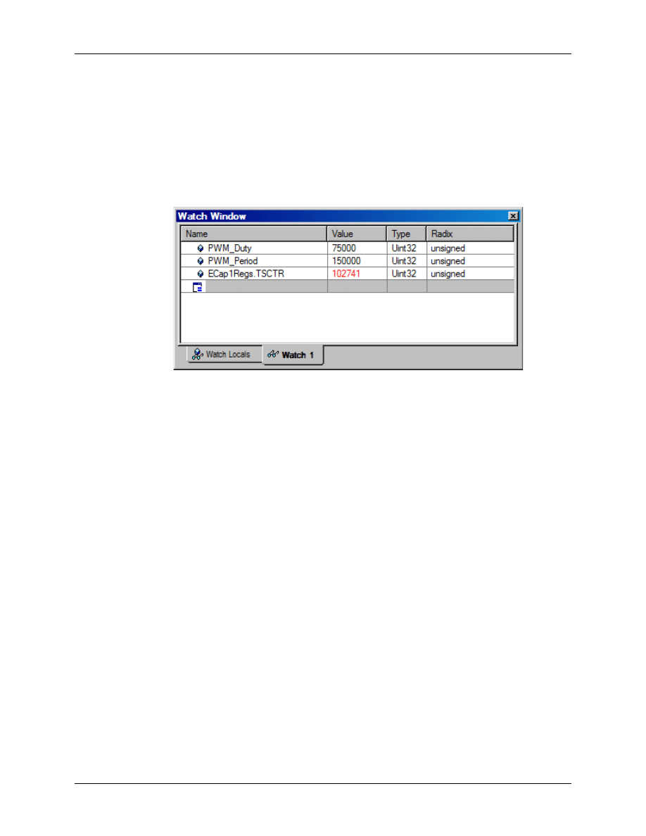
Lab7_10: ePWM1A 1 kHz signal captured by eCAP1
F2833x - PWM and Capture Units
7 - 81
File
Load Program
14. Test the code:
GEL
Realtime Emulation Control Run_Realtime_with_Restart
15. Open the Watch Window and add the variables "PWM_Duty", "PWM_Period" and
"ECap1Regs.TSCTR" to it. With a left mouse click in the "Radix" column, we can change the
format to "unsigned" for all 3 variables. Now click right mouse in the Watch Window and
enable "Continuous Refresh".
What do the values in "PWM_Duty" and "PWM_Period" mean? Remember that ePWM1A is a
signal of 1 kHz with a period of 1 millisecond and a pulse width of 0.5 milliseconds. Our
measurement unit has a resolution of 1/150MHz = 6.667 ns. Therefore the value of 150,000 for
"PWM_Period" translates into 150,000 * 6.667 ns = 1 millisecond.
16. Finally halt the DSC:
GEL
Realtime Emulation Control Full_Halt_with_Reset
END of LAB 7_10
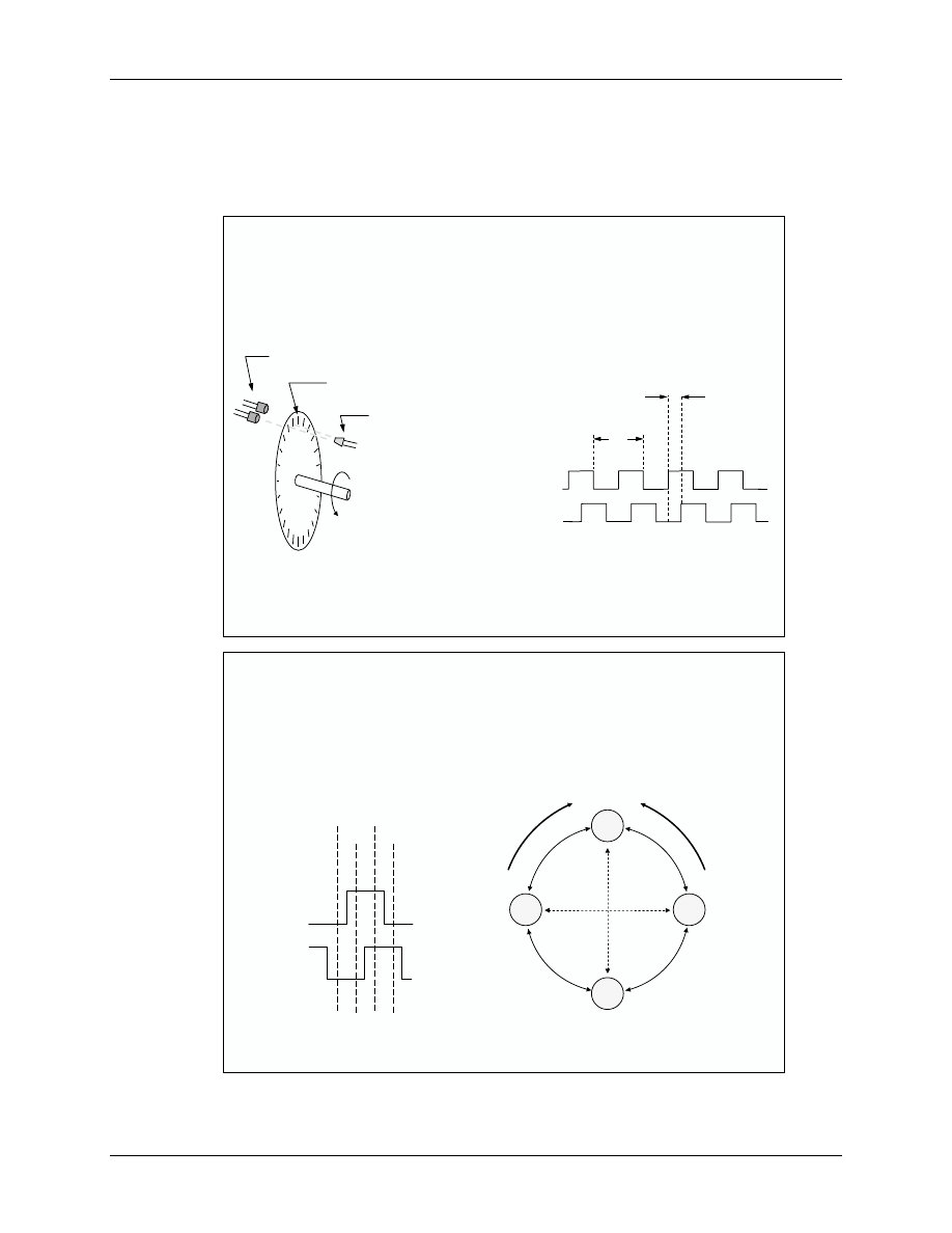
Enhanced QEP module
7 - 82
F2833x - PWM and Capture Units
Enhanced QEP module
The F28335 device contains to two enhanced Quadrature Encoder Positioning (eQEP) modules.
These modules are usually used as hardware support units for incremental encoder devices.
7
7
-
-
66
66
What is an Incremental
What is an Incremental
Quadrature
Quadrature
Encoder?
Encoder?
A digital (angular) position sensor
A digital (angular) position sensor
slots spaced
θ
deg. apart
photo sensors spaced
θ
/4 deg. apart
light source (LED)
shaft rotation
Ch. A
Ch. B
Quadrature Output from Photo Sensors
θ
θ
/4
Incremental Optical Encoder
7
7
-
-
67
67
How is Position Determined from
How is Position Determined from
Quadrature
Quadrature
Signals?
Signals?
Ch. A
Ch. B
(00) (11)
(10) (01)
(A,B) =
00
01
11
10
Quadrature Decoder
State Machine
increment
counter
decrement
counter
Position resolution is
θ
/4 degrees
Illegal
Transitions;
generate
phase error
interrupt
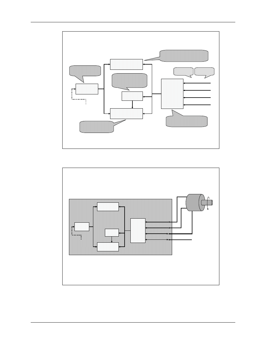
Enhanced QEP module
F2833x - PWM and Capture Units
7 - 83
7
7
-
-
68
68
eQEP
eQEP
Block Diagram
Block Diagram
Quadrature
Quadrature
Decoder
Decoder
EQEPxA
EQEPxA
/XCLK
/XCLK
EQEPxB
EQEPxB
/XDIR
/XDIR
EQEPxI
EQEPxI
EQEPxS
EQEPxS
Position/Counter
Position/Counter
Compare
Compare
Quadrature
Quadrature
Capture
Capture
32
32
-
-
Bit Unit
Bit Unit
Time
Time
-
-
Base
Base
QEP
QEP
Watchdog
Watchdog
SYSCLKOUT
SYSCLKOUT
Generate the direction and
clock for the position counter
in quadrature count mode
Generate a sync output
and/or interrupt on a
position compare match
Measure the elapsed time
between the unit position events;
used for low speed measurement
Generate periodic
interrupts for velocity
calculations
Monitors the quadrature
clock to indicate proper
operation of the motion
control system
Quadrature -
clock mode
Direction -
count mode
The QEP is used (a) to estimate the speed and direction of a rotation or (b) to perform a
positioning movement.
7
7
-
-
69
69
eQEP
eQEP
Connections
Connections
Ch. A
Ch. B
Index
Quadrature
Decoder
EQEPxA/XCLK
EQEPxB/XDIR
EQEPxI
EQEPxS
Position/Counter
Compare
Quadrature
Capture
32-Bit Unit
Time-Base
QEP
Watchdog
SYSCLKOUT
SYSCLKOUT
Strobe
from homing sensor

Infrared Remote Control
7 - 84
F2833x - PWM and Capture Units
Infrared Remote Control
An interesting example for the capture unit is an infrared (IR) remote receiver. IR-signals are
widely used for all kinds of handheld remote control devices, such as TV, radio tuners and
amplifiers, DVD players, satellite receivers and many others. On the Peripheral Explorer Board
an IR - sensor (TSOP32238 - http://www.vishay.com) is connected to capture unit ECAP4
(GPIO27). This unit will be used to measure the pulse widths of each pulse in a series sent to the
IR-receiver.
IR - Protocols
Although IR-remote is widely used in consumer electronics, there are different and incompatible
protocols. In a typical living room, you will usually find a collection of different remote control
units:
Typical IR protocols are:
•
RC5 code:
•
designed by Philips and also used by Loewe, Bang & Olufsen, Bose,
Grundig, Marantz, Hauppauge, in model making and other areas
•
14 - Bit code to address up to 32 devices with 64 instructions each
•
SIRCS/ CNTRL - S Code:
•
designed by Sony
•
up to 21 data bits
•
DENON code:
•
16 bit transmission
•
MOTOROLA - Code:
•
Similar to RC5
•
11 bit transmission
•
For our exercise we will focus on RC5 code.
RC5 protocol
A RC5 protocol consists of 14 bits per transmission:
•
2 Start Bits (always '1'). Used to synchronize the transmission and to adjust the amplification
of the receiver.
•
1 Toggle Bit (alternate '1' or '0'). Level is changed each time a button is pressed. Used to
distinguish between a long duration (permanent pressing of a button) and a repetitive use of a
button.
•
5 address bits. Allow the control of up to 32 devices by the same control unit.
00
TV1
01
TV2
02
Videotext
03
Video VD
04
Video LV1
05
VCR1
06
VCR2
07
experimental
08
Sat-Receiver
09
Camera
10
Sat-Receiver 2
11

Infrared Remote Control
F2833x - PWM and Capture Units
7 - 85
12
Video-CD
13
Camcorder
14
15
16
Audio-
Amplifier 1
17
Receiver /
Tuner
18
Audio Tape Re-
corder
19
Audio-Amplifier 2 /
experimental
20
CD-Player
21
record player
22
23
DAT-Tape, MD-
Recorder
24
25
26
CDR
27
28
29
lighting
30
lighting 2
31
Telephone
00
"0"
01
"1"
02
"2"
03
"3"
04
"4"
05
"5"
06
"6"
07
"7"
08
"8"
09
"9"
10
11
12
Standby
13
Mute
14
Default Setup
15
16
Volume +
17
Volume -
18
Brightness +
19
Brightness -
20
Color +
21
Color -
22
Bass +
23
Bass -
24
Highs +
25
Highs -
26
Balance right
27
Balance left
28
29
30
31
32
33
34
35
36
37
38
39
40
41
42
43
44
45
46
47
48
Pause
49
50
<<
51
52
>>
53
Play
54
Stop
55
Record
56
57
58
59
60
61
62
63
System select
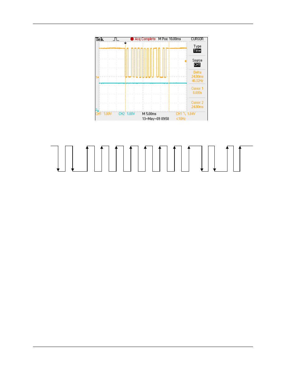
Infrared Remote Control
7 - 86
F2833x - PWM and Capture Units
The figure above shows the pattern for the "POWER" - Button of the PHILIPS universal remote
control, as supplied with the Peripheral Explorer Board. RC5 is a bi-phase code with duration of
1778µs for a single bit. The following figure will explains the details:
1
1
0
0 0 0 0 0 0 0 1 1 0 0
Start -C6 T A4 A3 A2 A1 A0 C5 C4 C3 C2 C1 C0
This screenshot translates into address = 0 (TV) and command = 12 (ON/OFF/STANDBY). We
will use this command in Lab7_11 to toggle LED LD2 of the Peripheral Explorer Board each
time the POWER button of the remote control is pushed.
The space between the signal edges is either 889µs or 1778µs.
The RC5 idle separator between transmissions sequences is defined as 113ms.
We will use eCAP4 unit to capture four consecutive edges, in the sequence "falling - rising-
falling - rising" and repeat this four edges capture until the end of the pulse series. After the
capture of a full command, Lab7_11 must then decode the code and in case of address = 0 and
code = 12 toggle led LD2.

Lab7_11: eCAP4 to receive a RC5 IR-signal
F2833x - PWM and Capture Units
7 - 87
Lab7_11: eCAP4 to receive a RC5 IR-signal
Objective
The F28335ControlCARD is used in combination with the Peripheral Explorer Board to receive a
RC5 sequence (Phillips-Specification) from an IR remote control unit.
Procedure
Open Project File
1. In the project "Lab7", open the file “Lab7_1.c” and save it as “Lab7_11.c”
2. Add “Lab7_11.c” to the project and exclude “Lab7_10.c” from build. Use a right mouse click
on file “Lab7_10.c”, select “File Specific Options”; in category “General” enable “Exclude
from Build”.
3. Add the provided source code file "Lab7_11_IR.c" to your project. This file is located in
directory \Labs\Lab7.
Edit Source File
4. In Lab7_11.c search for function "Gpio_select()" and select eCAP4 function for pin GPIO27,
which is connected to the IR-receiver TSOP32238.
5. At the beginning of "Lab7_11.c", add two new function prototypes for external functions:
extern void Calculate_IR_code(void);
extern interrupt void eCAP4_isr(void);
6. Also add a new function prototype for local function:
void Setup_eCAP4(void);
7. Add the following global variables:
Uint16 result[100];
// distances between edges
Uint16 signal_IR_ready=0;
// decode switch
Uint16 IR_address;
// IR device address
Uint16 IR_command;
// IR command
Uint16 IR_Toggle;
// status of IR - Toggle bit
8. In “main()”, after the basic initialization of the PIE vector table, add a line to load the address
of our local interrupt function "eCAP4_isr" into the PIE vector table:
PieVectTable.ECAP4_INT = &eCAP4_isr;
Remember that this memory location is EALLOW protected!
9. In “main()”, after the initialization of CPU Timer 0, add a for-loop to clear all elements of
array "result[100]".
10. Next, add a line to enable the PIE - interrupt line for eCAP4:

Lab7_11: eCAP4 to receive a RC5 IR-signal
7 - 88
F2833x - PWM and Capture Units
PieCtrlRegs.PIEIER4.bit.INTx4 = 1;
11. Modify the line to initialize register IER accordingly! Recall that eCAP4 is controlled by line
INT4!
12. In the endless while(1) loop of “main()”, after the wait construction to wait for 100
milliseconds, add the following code:
if (signal_IR_ready == 1)
{
Calculate_IR_code();
if(IR_command == 12) GpioDataRegs.GPATOGGLE.bit.GPIO11 = 1;
for (i=0;i<100;i++) result[i] = 0;
signal_IR_ready = 0;
}
13. At the beginning of “main()”, add a local integer variable "i".
14. In “main()”, after the function call to "Gpio_select()", add a function call to a new function
"Setup_eCAP4(). We will define this function shortly.
15. At the end of "Lab7_11.c", add the definition of function "Setup_eCAP4()". Take into
account:
•
In register ECCTL1:
•
Set Polarity for CAP1 to 4 to: falling - rising - falling - rising
•
Select difference mode or "delta" mode for all 4 capture events
•
Enable loading of CAP registers
•
Do not use the prescale feature
•
For register ECCTL2 initialize:
•
Enable Capture mode
•
Disable all synchronization signals
•
For TSCTRSTOP select free running mode
•
Select continuous mode
•
Set Stop_Wrap to wrap after capture event 4
•
For register ECEINT:
•
Enable Interrupt after the 4th event.
Build, Load and Test
16. Build and Load the modified project.
•
Project
Rebuild All
•
File
Load Program
17. Test the code:
•
GEL
Realtime Emulation Control Run_Realtime_with_Restart
Now Use an IR-Remote control Unit with RC5 - code (Phillips, Loewe) and press the "ON/OFF"
- key in front of the IR-Receiver at the Peripheral Explorer Board.

Lab7_11: eCAP4 to receive a RC5 IR-signal
F2833x - PWM and Capture Units
7 - 89
Each time you press the "POWER" - button of the remote control, LED LD2 (GPIO11) at the
Peripheral Explorer Board should toggle.
END of LAB 7_11
Note:
•
HRPWM - mode was not discussed in this chapter, because to experiment with it would require an expensive and fast
oscilloscope.

Lab7_11: eCAP4 to receive a RC5 IR-signal
7 - 90
F2833x - PWM and Capture Units
This page has bee left blank intentionally.
Document Outline
- F2833x PWM, Capture and QEP
- Introduction
- Module Topics
- ePWM Block Diagram
- ePWM Time Base Unit
- ePWM Phase Synchronisation
- Timer Operating Modes
- Time Base Registers
- Lab 7_1: Generate an ePWM signal
- Lab 7_2: Generate a 3 - phase signal system
- Purpose of Pulse Width Modulation
- ePWM Compare Unit
- ePWM Action Qualification Unit
- Lab 7_3: A 1 kHz signal with variable pulse width
- Lab 7_4: a pair of complementary 1 kHz-Signals
- Lab 7_5: Independent Modulation on ePWM1A / 1B
- ePWM Dead Band Module
- Lab 7_6: Dead Band Unit on ePWM1A / 1B
- ePWM Chopper Module
- Lab 7_7: Chopped Signals at ePWM1A / 1B
- ePWM Over Current Protection
- Lab 7_8: Trip Zone protection with TZ6
- ePWM Interrupt Sources
- Lab7_9: ePWM Sine Wave Modulation
- eCAP Capture Module
- Capture Units Registers
- Lab7_10: ePWM1A 1 kHz signal captured by eCAP1
- Enhanced QEP module
- Infrared Remote Control
- Lab7_11: eCAP4 to receive a RC5 IR-signal
Wyszukiwarka
Podobne podstrony:
Module 07
EdPsych Modules PDF Cluster 2 Module 07
Assertivness Module 07
CE Elementary module 07 web worksheet
07 cisco semestr 2 v31 module 7 exam
07 OnScreen B1plus Module 7
07 BS Module 1 Section 7
07 cisco semestr 3 v31 module 7 exam
EŚT 07 Użytkowanie środków transportu
07 Windows
07 MOTYWACJAid 6731 ppt
Planowanie strategiczne i operac Konferencja AWF 18 X 07
Wyklad 2 TM 07 03 09
ankieta 07 08
więcej podobnych podstron