
CAN ON THE AVR
by Mike Blenderman
Draft 1.2 prerelease

CAN on the AVR – Draft 1.2 prerelease
Page 1
Table of Contents
Introduction...................................................................................................................................................................1
CAN Description ...........................................................................................................................................................1
Starting Development Tips.............................................................................................................................................2
Clock Source .................................................................................................................................................................3
CAN Bus Length ...........................................................................................................................................................3
Message ID Details........................................................................................................................................................4
Priority Arbitration ........................................................................................................................................................5
Errors ............................................................................................................................................................................7
Acceptance Filter...........................................................................................................................................................7
Initialization and Use .....................................................................................................................................................9
Baud Rate....................................................................................................................................................................10
Interrupts.....................................................................................................................................................................11
Appendix A - Baud......................................................................................................................................................14
Introduction
This is not an ATMEL Incorporated document, however it does provide supplemental information to the ATMEL AVR
AT90CAN32/64/128 data sheet. The current data sheet revision at the time this document was created is 7679C-CAN-
01/07. It is assumed you have already read the data sheet and read at least some of the Bosch 2.0 CAN specification found
on the Bosch web site. There is additional information on setting up CAN baud rates available on the Bosch web site
(BTW, big kudos to Bosch for freely publishing the CAN specifications).
CAN Description
CAN is a multi-cast, multi-master serial network bus. Multi-cast means all the CAN nodes see all the CAN network data
traffic (this is also called a broadcast bus). You cannot route CAN data between specific nodes like a point-to-point network
does (traditional network cut switches and routers do not work for CAN). Multi-master means any CAN node may send
data on the CAN bus. Ultimately only one master at a time is allowed to complete an entire CAN bus frame. CAN has a
neat trick that allows dynamic real time priority arbitration when more than one master collides with another master and
sends data at the same time. All the CAN nodes that loose the priority arbitration simply go back into receive which
prevents having the winning master re-send any CAN bus data. Many other types of serial networks require the master to
always send the data over again until there is no data collision with any other masters.
Since CAN is a real time control protocol it only allows a maximum of up to 8 data bytes per CAN data frame. Breaking up
the data frames into small pieces allows other CAN nodes quick access to the CAN bus. The fixed 8 byte maximum size
also allows the designer to calculate the maximum response time for a complete maximum length message and estimate the
overall CAN data frame response. You may calculate this bus response for the highest priority CAN data frame on a
correctly configured CAN bus that is operating without errors. Worst case response can be estimated depending on
expected error behavior, other bus traffic loads and priorities. This will give you a reasonable idea of the real time response
limitations. For example: if you are using CAN to control engine spark plug firing sequences, you must make sure your
CAN bus design will be able to keep up with any and all timing demands of the engine. More is at stake here than just raw
bit rate speeds. Other network types that are faster may not support built-in features like automatic global error reporting for
network wide data integrity, error confinement of a malfunctioning bus node, collision arbitration without retries, built-in
limits on data frame sizes that prevent bus access blocking by huge (long) continuous data transfer streams, automatic
retires, etc.
CAN is a message oriented network, not an address oriented network. There are no dedicated CAN node addresses or

CAN on the AVR – Draft 1.2 prerelease
Page 2
unique identification built into the Media Access Control (MAC) layer. You may simulate an addressable bus by using
software to assign a unique Rx Message ID to an individual CAN node. However, if for no other reasons than the priority
arbitration and global error signaling, you cannot isolate any CAN bus node from the any other CAN bus nodes. You may
use multiple CAN buses with a CAN bus bridge between them, but the bridge will require individual complete CAN nodes
for each separate CAN bus (i.e. the separate CAN buses must remain physically separated). It is the job of the CAN bus
designer to figure out the Message ID assignments for each CAN node. If needed, a higher level protocol like CANopen
(CANfestival), CANKingdom, DeviceNet for example or an in house protocol may be used. Using an already specified
protocol should provide the Message ID assignment scheme for you, but it could be a large amount of work to port an
existing standard to the AVR processor and/or you might have to pay money for the specification.
The entire CAN bus acts together in concert. If a CAN message is sent and even one single CAN node has a problem with
it, the entire CAN bus will be alerted to that error. Any CAN message sent is always a two-way communication between all
the CAN nodes. If there are no errors in the CAN message, then the return response will be the ACK bit. If there is an error,
then CAN has different ways of signaling the error to all the other CAN nodes and the return response is more complex.
CAN is very picky about baud rates and setting the CAN baud rate is complicated. Every CAN node on the same CAN bus
must have the exact same baud rate. Unlike other serial data devices such as USARTs, the behavior of all the other CAN
nodes connected to the CAN bus really does matter.
The CAN specification does not say exactly what the physical CAN bus is, but it does have certain requirements that must
be met. One requirement is the zero value dominant and one value recessive behavior, where a dominant always prevails
over a recessive. There are different ISO specifications and other specifications that do require a particular bus hardware
implementation. These are basically extensions added onto, but not part of the Bosch CAN specification.
Common CAN transceiver interface chips are available that use differential 120 ohm impedance copper wiring. An
advantage of these compared to multi-master RS-485 driver chips is bit collisions do not cause bus short circuit conditions.
Since RS-485 actively drives both high/low bus data states, any nodes sending different bit values at the same time will
drive the bus positive voltage source on a node directly into ground on another node. These CAN bus drivers only actively
drive the dominant bus state and leave the recessive state to pull up and pull down resistors that are always connected. Any
CAN nodes sending different bit values at the same time will not drive a positive bus voltage on one node directly into a
bus ground from any other node. The manufacturer of the CAN transceiver interface chip will specify how many chips may
be connected together (i.e. the number of fanout loads). Some of these CAN chips offer slew rate limiting to reduce radiated
noise from the CAN bus wiring. The amount of output driver slew rate limiting is balanced with the CAN baud rate (see the
CAN transceiver chip data sheet).
There is a variation on the usual CAN priority arbitration scheme called Time Triggered CAN (TTCAN). Automatic Tx
retries are disabled in TTCAN and CAN Tx nodes use a time slot to transmit in. If you want to use TTCAN, you will need
other/additional information sources to learn about it.
Starting Development Tips
When developing brand new CAN driver software from scratch, start with a slower CAN baud rate. This allows for less
than perfect CAN bus wiring impedance and termination. If you want to, turn up the CAN bus speed after your new drivers
are working.
When developing CAN drivers, pay very close attention to the data sheet read only bit or bits in the register descriptions. It
will save you the embarrassment of finding out later during debugging that you have been writing to a read only register or
a read only bit in a register as if you expected writing to it would do something. Paying attention and identifying the read
only bits will also help you understand what those bits are used for.
The AT90CAN32/64/128 will not acknowledge its own CAN messages. You cannot send a CAN frame to the same AVR
chip. You will get an acknowledge error if you try this with only a single CAN node. Using the CANGCON register

CAN on the AVR – Draft 1.2 prerelease
Page 3
LISTEN bit has no effect on the lack of an acknowledge. Since you need at least two different CAN nodes, it will be easier
if you have a CAN analyzer or at least one already working CAN node to use for testing when developing new CAN driver
software.
If you do not have an ICE50, JTAGICE MKII, DRAGON or JTAGICE for debugging, there is an AVRstudio CAN plug-in
for software CAN simulation. However, like most software simulators it might possibly have some problems with
something as complex as CAN. The original JTAGICE has a “limited” notation on the AT90CAN128 device support
documentation, with no explanation of exactly what limited means The original JTAGICE does not support the
AT90CAN32/64 chips. The DRAGON is by far the most economical fully functional debugging hardware, but it will only
do ICE with the AT90CAN32 CAN chip because of its 32 K FLASH size ICE support limit. The more expensive
JTAGICE MKII is the best all around ICE debugger that supports all JTAG and debugWIRE capable AVR chips. The
ICE50 is a really expensive traditional type of ICE that requires purchasing an additional emulator pod for each type of
AVR chip that is used, but it does offer additional features not available with any JTAG based ICE.
Do not forget to read the errata section in the data sheet. You should also look for any AVR Forum errata sticky threads.
The AVR CAN module is based on the older C51/CAN module. There is an AVR application note on migrating from the
C51/CAN chips to the AT90CAN32/64/128 chips. This application note may be used to port program code from the
C51/CAN to the AVR/CAN and therefore expands the potential amount of example program code as well. There are
AT90CAN32/64/128 CAN program examples and a CAN library available on the ATMEL web site. Even if the example
code does not do exactly what you want, you may still strip out the low level CAN interface code from the example code to
start your own program with. The AVRfreaks Forum as well as your favorite Internet search engine are also great
resources. In general as a rule of thumb, always evaluate the quality and completeness of any example code, as there are
usually no guarantees on how well it was written and/or if it is suitable for your exact application.
Clock Source
For the most part CAN requires a crystal oscillator to generate an accurate, stable CAN asynchronous baud rate. This is
especially true at higher CAN baud rates (1 mega-baud is the maximum). Using ceramic resonators at slower baud rates is
possible, but adds to the design burden in order to engineer a working CAN system. As long as all the CAN nodes use the
exact same baud rate, you may select your own CAN baud rate and choose an AVR main oscillator frequency that perfectly
divides down to that exact baud rate (even if that baud rate is not an integer value with no remainder). Because a minimum
of 8 time quanta are required for each CAN bit time (i.e. baud rate), the AVR I/O clock frequency divided by 8 is the fastest
possible CAN baud rate. This means at least an 8 MHz AVR clock is required to achieve the maximum CAN one mega-
baud rate and that AVR clock will have to be increased in order to use a time quanta setting higher than 8 at the maximum
CAN baud rate. If you are also using the AVR USART module or TWI module, these other asynchronous baud rates are
secondary to the CAN baud rate when choosing the AVR main oscillator frequency. CAN specifies an oscillator tolerance
of 0.5 % at full speed with the specified protocol and up to 1.58 % maximum at 125 k-baud or less using a modified
protocol. Out of specification baud rate errors between different CAN nodes may also have the effect of reducing the
maximum CAN bus length, if the CAN bus is even capable of operating under those conditions. Unlike USARTs, CAN
does not tolerate built in (i.e. purposely-selecting) baud rate errors between the different CAN nodes. Designing each CAN
node for exactly the same baud rate allows for normal production differences between the different CAN nodes (like an
AVR clock crystal that is not exactly on frequency but is close enough, environmental temperature variations, etc.).
CAN Bus Length
The CAN bus has physical length limits based on the maximum propagation delay time between all nodes vs. baud rate (i.e.
CAN bit time). The internal propagation delay of the CAN driver circuits is a factor as well as the propagation delay caused
by the CAN bus serial data traveling over the physical length of the CAN bus. All CAN nodes must detect the same bit
together, and any CAN node from anywhere along the CAN bus might also be setting that same bit value. When the longest

CAN on the AVR – Draft 1.2 prerelease
Page 4
propagation delay time becomes a significant part of the time for each CAN bit time (i.e. baud rate), it limits the detection
window time across the entire CAN bus for each individual CAN bit. Since the internal propagation delay of the CAN
circuitry is not adjustable without redesigning the hardware, the physical length of the CAN bus is limited to keep the total
propagation delay within requirements. Simply put, higher CAN baud rates have shorter CAN bit times and therefore
require shorter CAN bus lengths.
The CAN baud rate setting has a propagation time segment that sets the phase error compensation. This phase error may
also be due to slight oscillator frequency differences in other CAN nodes as well as the CAN bus propagation delay. The
amount of phase adjustment which is set as integer multiples of time quanta, along with critical internal CAN bit timing
requirements, also contribute to the bus length limitations (see the Bosch CAN baud white paper for more information).
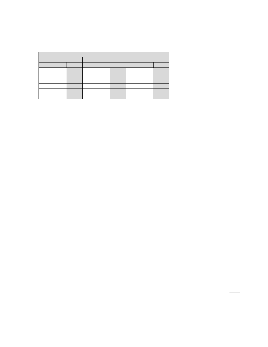
Recommended Practical CAN Maximum Bus Lengths*.
bit rate kbps
Bus length (m)
1000
30
500
100
250
250
125
500
62.5
1000
20
2500
10
5000
* Theoretically achievable CAN bus lengths may be longer.
Message ID Details
From the Bosch version 2.0 Sept. 91 Part A page 11: The 7 most significant bits (ID-10 - ID-4) must not be all ’recessive’.
This limits the range of 11 bit CAN Message IDs from 0x000 to 0x7EF. Message ID values from 0x7F0 to 0x7FF are not
allowed (this is 16 unusable Message ID values total, with 2032 usable Message ID values left).
Some CAN systems may reserve the Message ID 0x7EF as a special wake up from sleep message (as suggested in the
Bosch CAN specification). Since the AT90CAN32/64/128 has no CAN Message ID recognition ability while in sleep, this
is mostly of interest for compatibility with other CAN hardware. Still, for example it is certainly possible to implement an
AVR simple external interrupt wake up on any CAN bus activity using one of the INT0 through INT3 input inputs. This is
an easy solution to using sleep with the AT90CAN32/64/128 CAN module.
From the Bosch version 2.0 Sept. 91 Part B page 44: The 7 most significant bits (ID-28 - ID-22) must not be all ’recessive’.
This limits the range of 29 bit CAN Message IDs from 0x00000000 to 0x1FBFFFFF. Message ID values from
0x1FC00000 to 0x1FFFFFFF are not allowed (this is 4,194,304 unusable Message ID values total, but don't worry because
there are still 532,676,608 usable Message ID values left).
CAN on the AVR – Draft 1.2 prerelease
Page 5
Priority Arbitration
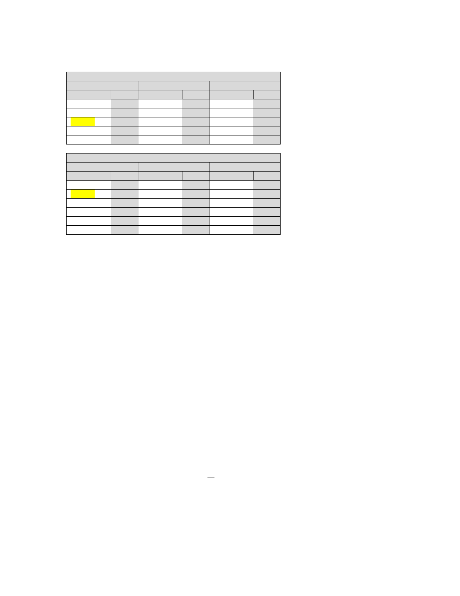
CAN Priority Arbitration Bits
11 bit Message ID
29 bit Message ID
Mixed 11/29 bit
Name
Bits
Name
Bits
Name
Bits
IDTn
11
IDTn
(MSb)
11
IDTn
(MSb)
11/11
RTR
1
*
-
RTR/SRR
1/ -
-
IDE
1
IDE
1/1
-
IDTn
(LSb)
18
IDTn
(LSb)
-/18
-
RTR
1
-/RTR
-/1
total bits
12
total bits
31
total bits
13/31
* The fixed one value recessive SRR bit is not counted in the 29 bit Message ID since it is just a place holder bit for the relocated RTR bit in
the 29 bit CAN format. However, in mixed 11/29 bit format priority arbitrations the recessive SRR bit may be compared to the 11 bit format
RTR bit.
All of the above 11 bit Message ID, 29 bit Message ID and Mixed 11/29 bit Message ID bits represent live CAN Remote
Frame or CAN Data Frame serial data bits from more than one CAN node sending at the same time. The bit names are
taken from the data frame and remote frame drawings in the data sheet. Since the CAN bus synchronizes the start of all the
sending CAN nodes to start each frame together at the same bit time slot, each CAN node sends the same type of bit at the
same time slot. The IDTn bits are numbered differently for the 11 bit and 29 bit formats. They are IDT10 through IDT0 for
the 11 bit format and IDT28 through IDT0 for the 29 bit format. All IDTn bits are sent starting from the Most Significant
Bit to the least significant bit. In the mixed 11/29 bit comparison, the 11 bit format IDT10 is compared to the 29 bit format
IDT28 and on down until IDT0 and IDT18 (the first 11 IDTn bits) are compared. The RTR bit time slot is different
between the 11 bit and 29 bit formats. The IDE bit is only part of the arbitration field when a 29 bit format is involved.
Priority arbitration is a bit wise operation on the CAN frame arbitration field bits. Since a dominant bit value always
overrides a recessive bit value, every CAN node reads each bit as it sends each bit. Whenever a recessive value is sent, but
a dominant value is read, that Tx CAN node instantly knows it has collided with another Tx CAN node. During arbitration
this means the recessive sender looses arbitration and reverts back to just receiving the current CAN frame, without loosing
any data. This is a non-destructive bit wise collision detection and no retries are needed to send the arbitration field bits
again. First, the 11 most significant IDTn Message ID bits are compared for all formats. Next the 11 bit format will
compare the RTR bits and is then finished with the arbitration field. The mixed 11/29 bit format will compare the RTR bits
with the fixed value SRR bits. Both 29 bit and mixed 11/29 bit formats will compare the IDE bits next. In the case of a
mixed 11/29 bit format, the priority arbitration is finished at this point for all 11 bit format Message IDs (more info on this
below). The 29 bit format will proceed to compare the 18 remaining least significant IDT Message ID bits, finally compare
the RTR bits and the priority arbitration is finished. Any CAN node detecting any bit collision during priority arbitration
(i.e. reads a dominant bit value when it sent a recessive bit) will loose arbitration, stop sending and revert to just being a Rx
CAN node. The priority arbitration winner is the last CAN node that did not drop out due to loosing a recessive send
against a dominant reception. Because dominant zero values always win over recessive one values, lower bit values win
arbitration.
When using mixed 11/29 bit priority arbitration, any 11 bit format Message ID that survived all the IDTn bits and RTR bit
arbitration always wins the final arbitration when the IDE bit is checked. If all the 11 bit format Message IDs loose
arbitration and drop out during the IDTn arbitration checks, then a normal 29 bit format Message ID arbitration will
proceed after the IDE bit (i.e. the mixed arbitration always ends after the IDE bit, but a 29 bit format arbitration may
continue only against other 29 bit CAN Message IDs). This means at no time will an 11 bit format Message ID be
arbitrated past the 13th bit, which is a good thing since the 11 bit format is all out of arbitration field bits after this point.
The IDE bit is part of the 29 bit CAN Message ID priority arbitration. The 29 bit format IDE bit position is specifically
arranged and assigned a recessive value while the 11 bit format IDE bit position is always a dominant value. So, the mixed
arbitration of both 11 bit and 29 bit CAN Message IDs will never proceed beyond the IDE bit position if any surviving 11
bit format CAN nodes are still sending. Keep in mind that in order for the 11 bit format part of the arbitration process to

CAN on the AVR – Draft 1.2 prerelease
Page 6
make it all the way to the IDE bit, the 11 bit CAN Message ID recessive bits (IDT10-IDT0) must perfectly match the other
29 bit format recessive CAN Message ID bits (IDT28-IDT18) and the 11 bit format RTR bit must be recessive. If any of
these individual IDT bits or the RTR bit have a zero dominant value and a one recessive value bit wise mismatch, the one
with the first zero value dominant bit will win that particular bit arbitration (i.e. the looser will drop out) before the IDE bit
is arbitrated.
Consider these two different message identifier values:
0x015 (IDT10-IDT0) – 11 bit Message ID (21 decimal)
0x0500000 (IDT28-IDT0) – 29 bit Message ID (5,242,880 decimal)
First lets break down the 11 Most Significant Bits and use a common 4 bit nibble hex alignment between the first 11 bits of
these 11 bit and 29 bit formats.
000 0001 0101 (binary 11 bit format adjusted to place the MSb first)
000 0001 0100 000000000000000000 (binary 29 bit format adjusted to place the MSb first)
0x015 (IDT10-IDT0) – 11 bit Message ID
0x014 (IDT28-IDT18) – 29 bit Message ID (only the first 11 bits)
Because the first 11 bits of the 29 bit format message identifier 0x014 (IDT28-IDT18) are a lower value than the 11 bits of
the 11 bit format message identifier 0x015 (IDT10-IDT0), the 29 bit format message identifier wins the bit wise priority
arbitration, even though its total 5,242,880 decimal numerical value (IDT28-IDT0) is much larger than the 11 bit format
message identifier numerical value of 21 decimal (IDT10-IDT0). The 29 bit format Message ID value must be larger than
0x003FFFF before the IDT28 through IDT18 part of its value is no longer zero. In reality, 29 bit format Message Identifiers
lower than 0x0040000 win mixed arbitration unless the 11 bit format Message ID value is zero.
The above binary representation clearly shows where the recessive 11 bit format IDT0 bit looses to the dominant 29 bit
format IDT18 bit (this bit is underlined). When counting these bit positions, keep in mind they are numbered starting from
zero in the IDTn representation. So, counting bit positions from one, starting from the right LSb position, the IDT18 bit is
in the 19th bit position.
Of course when 11 bit formats are only arbitrated against other 11 bit formats, the lower numbered Message ID always
wins. A remote frame will loose out to a data frame because the RTR bit is zero for a data frame. This will behave the same
way when 29 bit formats are only arbitrated against other 29 bit formats. The arbitration priority behavior is much simpler
when mixed 11/29 bit formats are not arbitrated against each other.
After the arbitration field, any Tx bit collisions are considered to be errors and indicated as a bit error (BERR). The
exceptions to this are during the ACK time slot and while sending a passive error flag.
Only unique CAN Message ID and RTR bit values may be transmitted by any CAN node. If two or more Tx CAN nodes
using the exact same CAN Message ID and RTR values collide, they will both pass the priority arbitration together
allowing two or more active CAN nodes to be sending after the arbitration field. After the arbitration is finished, any
dominant/recessive bit wise difference will cause a CANSTMOB register Tx BERR (Bit ERRor) in the transmitting CAN
node that sends a recessive bit and sees a dominant bit value instead (two BERR exceptions have already been noted).
Because CAN has error signaling, error node confinement and automatic retries of corrupted messages, the BERR will
cause an error flag to be sent over the entire CAN bus (error signaling). Automatic retries could theoretically create a
situation where the two Tx CAN duplicate Message ID+RTR nodes keep repeating the same BERR failure over and over,
until the Tx CAN node bus off error handling is triggered by the CANTEC error counter trying to exceed a value of 255
decimal. The CANTEC error counter is incremented by 8 when sending the error flag, so if there are no other Tx problems
the 32nd failed BERR retry attempt will cause the bus off (error node confinement). Since bus off is automatically reset
after receiving 128 occurrences of 11 consecutive recessive bits, the problems may keep occurring over and over. Just

CAN on the AVR – Draft 1.2 prerelease
Page 7
remember this problem is caused by the CAN bus designer using the exact same Tx CAN Message ID and RTR bit values
in multiple Tx CAN nodes (it is not the fault of the CAN system). Of course the exact same Rx CAN Message ID may be
used in any other CAN node or even in all the other CAN nodes.
Errors
Bosch recommends an error count greater than about 96 is an indication of a heavily disturbed CAN bus. Check the
CANREC and CANTEC register values for this error level. If high error level values persist, check your baud rate
calculations first. Incorrect baud rate settings have been sited as a primary cause of a heavily disturbed CAN bus. Because
there is a global error notification system for CAN, any errors will cause problems for the entire CAN bus, impact
throughput, cause error passive states and ultimately cause a bus off error node confinement. Unlike many USART drivers
that commonly ignore error flags and allow errors to pass, active CAN error detection does not ignore errors or allow errors
to pass, even on any other CAN nodes. When debugging CAN problems in general, knowing the values of the CANREC
and CANTEC error counters is critical. When asking for help or advice with a CAN bus sending or receiving problem,
these values are probably the first thing you will be asked about if you have not already provided them.
According to the Bosch CAN specification, there is no reason to increment the 8 bit CANREC error counter beyond a 128
decimal value. However, the 8 bit CANTEC error counter will go all the way to a 255 decimal value and cause a bus off
state if the count overflows.
CAN has a built in CRC check for data integrity. The active error signaling notifies all the CAN bus nodes if any node or
nodes encounter any error, which maintains the data integrity over the entire CAN network (I believe the data sheet CAN
opening paragraph called this “a very high level of security” which should not be confused with the more conventional use
of the word security as in encryption, etc.). This allows CAN nodes to assume all the other error active nodes have received
the same data. However, as with all electronic devices there is a specified undetected message error rate of 4.7 * 10
-11
.
Using redundant Rx CAN nodes on the same CAN bus will not necessarily decrease the undetected message error rate
because the built in CAN node CRC algorithm is probably responsible for at least a portion of the undetected message
error rate. Redundant Rx CAN nodes that use the same internal CRC algorithm will both share the same vulnerability of
failing to detect the same combinations of corrupted bits (no CRC based check is perfect). However, separate fully
redundant CAN buses could improve reliability. Sending critical information redundantly over and over in a continuous
loop is another defense (using otherwise idle CAN bus time with a very low priority back up Message ID). Any possible
undetected message errors would have a very short life span before one of the predominantly good messages overwrites the
very, very extremely rare undetected bad message. Including additional error detection information as data in each message
data frame is another defense against accepting corrupt data in the first place. Sending the same data two different ways
with different bit patterns is another verification step to avoid corrupt data. Since undetected error rates are extremely small,
they are usually not a problem and dealing with them is an entire endeavor all by itself.
Acceptance Filter
The acceptance filter is a CAN hardware mechanism that unburdens the AVR CPU from having to handle each and every
incoming received CAN message in real time. There are 15 Message Object buffers (MObs) that when setup to receive will
compare any CAN frames in the receive shift register with the information stored in each of the 15 MObs. This allows the
AVR CPU to only respond to CAN frames it is expecting (i.e. are accepted by the MOb) and ignore CAN frames not meant
for it (i.e. are not accepted by the MOb). The acceptance filter handles both 11 bit CAN and 29 bit CAN formats (the IDE
bit value determines the correct format). In addition there are mask bits that may be used to force a Rx bit wise true
comparison in the acceptance filter. In fact this mask may be used to force acceptance of all received CAN frames, if so
desired. The MOb mask only works for Rx MObs and has no meaning in a Tx MOb.
CAN on the AVR – Draft 1.2 prerelease
Page 8
Part A 11 bit Message ID CAN Rx Acceptance Filter Bits
CAN Rx Shift Reg.
1 of 15 Rx MObs
Each Rx MOb Mask
Name
Bits
Name
Bits
Name
Bits
IDn
11
IDTn
3
11
IDMSKn
7
11
RTR
1
RTRTAG
6
1
RTRMSK
9
1
IDE = 0
1
1
IDE
5
1
IDEMSK
9
1
RB0
1
RB0TAG
6
1
-
total bits
14
total bits
14
total bits
13
Part B 29 bit Message ID CAN Rx Acceptance Filter Bits
CAN Rx Shift Reg.
1 of 15 Rx MObs
Each Rx MOb Mask
Name
Bits
Name
Bits
Name
Bits
IDn
29
IDTn
4
29
IDMSKn
8
29
IDE = 1
2
1
IDE
5
1
IDEMSK
9
1
RTR
1
RTRTAG
6
1
RTRMSK
9
1
RB0
1
RB0TAG
6
1
-
RB1
1
RB1TAG
6
1
-
total bits
33
total bits
33
total bits
31
Note 1: The CAN Rx shift register IDE bit value of zero (dominant) determines the 11 bit Message ID format of the Rx CAN frame.
Note 2: The CAN Rx shift register IDE bit value of one (recessive) determines the 29 bit Message ID format of the Rx CAN frame.
Note 3: MOb registers CANIDT1 and CANIDT2.
Note 4: MOb registers CANIDT1, CANIDT2, CANIDT3 and CANIDT4.
Note 5: MOb register CANCDMOB.
Note 6: MOb register CANIDT4.
Note 7: MOb registers CANIDM1 and CANIDM2.
Note 8: MOb registers CANIDM1, CANIDM2, CANIDM3 and CANIDM4.
Note 9: MOb register CANIDM4.
The reserved bits RB0 and/or RB1 have no mask bits. According to the Bosch CAN specification, these reserved bit(s) are
always sent as zero dominant values for future compatibility purposes. The receiver is supposed to correctly receive either a
zero or one value, but you are never supposed to send a one value (at least not under the current specification). Because of
this, the reserved bit(s) in CANIDT4 are always set to zero. Because these reserved bit(s) are part of the control field and
not part of the priority arbitration field, they only effect the acceptance filter outcome.
When a new CAN Data Frame or CAN Remote Frame is received, each of the Rx enabled 15 MObs are searched for a
matching Message ID starting with the lowest numbered MOb to the highest numbered MOb. If more than one Rx enabled
MOb has a match to the new received CAN Frame, the only MOb used will be the lowest numbered MOb that matched.
The MOb Mask bits will either allow a full compare between the CAN data in the Rx Shift Register and the data in the
MOb, or they will force their individual bit to always be accepted as a match even when they do not really match. So, a
MOb Mask bit set to one allows the bit compare, and a MOb Mask bit set to zero forces the bit comparison to always
match. If an IDMSKn bit is set to zero, the forced true compare expands the total number of CAN Message ID values that
will match the acceptance filter. The expanded values depend on the binary weights of the IDTn bits forced into a true
match. If the IDEMSK bit is set to zero, the MOb will accept either 11 bit or 29 bit CAN Message IDs (see the previous
notes about mixed 11/29 bit format priority arbitration). If the RTRMSK bit is set to zero, the MOb will except either CAN
Data frames or CAN Remote frames. If all the Mask bits are set to zero, the MOb will accept any 11 bit, 29 bit, Remote
Frame or Data Frame with any CAN Message ID (i.e. all CAN data and remote frames).
If any Mask bits are set to zero and the MOb passes the acceptance filter (i.e. the MOb is selected), the actual received
value may be read from the appropriate AVR CAN register(s) in that MOb. This is because the CAN module automatically
writes the internal CAN Rx Shift Register values into the matching MOb registers when the acceptance filter finds a
matching MOb. If you allow mixed 11 bit and 29 bit CAN Message IDs, checking the CANCDMOB register IDE bit value

CAN on the AVR – Draft 1.2 prerelease
Page 9
will be critical for identifying the 11 bit or 29 bit received CAN frame formats. Without the IDE information, you will not
know what format to use when reading the four CANIDT registers. This also means if you allow a range of Message IDs,
you are able to tell which specific Message ID was actually received by reading the appropriate CANIDT registers after the
CANSTMOB register RXOK is asserted.
If an error is detected in a Rx CAN frame that matches the acceptance filter of any Rx MOb (starting with lower numbered
MObs), the error will be sent to that CANSTMOB MOb interrupt register. If an error is detected in a Rx CAN frame that
does not match the acceptance filter of any MOb, the error will be sent to the CANGIT general interrupt register instead.
This acceptance filter process is the reason the CANSTMOB and CANGIT registers have some duplicated Rx error bits
with the same meaning. Whenever an error occurs, the appropriate CANREC or CANTEC error counters will be
incremented. This error process has implications for the automatic error management and for automatic retires, so
additional things may also occur depending on the type of error.
Initialization and Use
In the AVR there are CAN general registers and CAN Message Object buffer (MOb) registers. The MOb registers are
used to setup a transmit (Tx) CAN frame or to receive (Rx) a CAN frame. There are 15 MOb register sets total and each
MOb register set is the same format/layout as all the other MOb register sets. The CANPAGE register is used as a pointer
register to select and access only one of the 15 MOb register sets by the CAN driver software. So, MOb registers must have
CANPAGE set first in order to access 1 of the 15 MOb register sets (numbered 0 through 14).The general registers are
normal I/O registers that are always available and do not need any pointer register to select them.
Initializing the AVR CAN controller requires a special sequence. All of the CAN general registers have an initial (default)
value. None of the MOb registers that use CANPAGE as an access pointer have an initial (default) value. As soon as the
CAN module is enabled (CANGCON register ENA/STB bit is set to a one) and actually starts (the read only CANGSTA
register ENFG bit becomes a one), the CANCDMOB register configuration bits (CONMOB1:0) information in all 15
MObs is immediately acted on. Since the CANDCMOB register bits have no initial (default) value, CAN chaos will ensue
if they have not already been explicitly initialized by your software. The correct initialization value is setting the
CONMOB1 and CONMOB0 bits to zero in each of the 15 MOb CANCDMOB registers before turning on the CAN
module. This is a MOb configuration “disable” value that starts the CAN module in a stable known state. The interrupt flag
bits should also be initialized to zero in each of the 15 MOb CANSTMOB registers. This will prevent false MOb interrupt
responses when the CAN module is turned on. The remaining MOb registers do not have to be initialized until their MOb is
actually going to be used. After this software setup and the initialization of the general CAN register values, the CAN
module may be safely enabled.
Before setting up an MOb for use (skipping the first initialization before the CAN module was turned on), the read only
CANEN2 and CANEN1 read only registers are used to see if the desired MOb is already in use or if its available for use.
Check this first to ensure you do not trample an active MOb operation that is already in progress. If you setup the MOb
register data while an MOb is active, the CAN controller may write to the MOb registers at any time while you are also
writing to the MOb registers. Ignoring the CANEN2 and CANEN1 registers is an invitation to create a bug in your program
that will not present symptoms consistently. The bug would only present when the MOb is written to by the CAN hardware
while you are also changing it, and even then there are lots of variable outcomes depending on what dynamically happens
to which bit values. Of course very simple CAN program software might do something simple with the MObs and not
appear to require checking the CANEN2 and CANEN1 registers. Just keep in mind that simple program code is often used
as the starting point for larger more complex programs. After all, checking these registers first is not a big burden for the
program anyway.
Frame buffer reception (CANCDMOB) is a special Rx mode that uses the CAN hardware to manage a block of two or
more MObs in a single AVR chip as an extended single receive buffer function. It has a complex setup and requires special
management as documented in the data sheet. If you ever see any need/desire to use this type of function, the equivalent
function may also be created in software using regular individual “enable reception” MObs instead.

CAN on the AVR – Draft 1.2 prerelease
Page 10
The CAN Remote Frame will tell another correctly setup CAN node to send an already setup prearranged CAN Data Frame
with the same Message ID (different RTR bit values). It triggers the other CAN node to send. This requires special setup
and management in both CAN nodes as documented in the data sheet. The same function may also be performed by your
CAN driver software using only CAN Data Frames instead. Be aware that some higher level protocols may not allow the
use of CAN Remote Frames even if they are available on your CAN hardware. Some of these protocols were originally
written in the early days, before Bosch specification version 2.0 and not all CAN chips will handle remote frames. I assume
this was only done for backward compatibility when using the protocol.
When using AVR CAN hardware with other manufacturers CAN hardware, you must make sure the other CAN hardware
matches the capabilities of the AVR and that the other CAN node has implemented these capabilities in their software. If it
does not, then you will have to limit which AVR CAN features you actually use in order to ensure both CAN nodes will
work together. This is usually only a problem when the other CAN node is not 2.0 Part A and/or Part B active capable (as
in an older CAN chip) or when a higher level protocol forbids using certain CAN capabilities.
It is recommended that you create a macro or function, which translates Message ID values from a straight numerical
format into the CANIDT1, CANIDT2, CANIDT3 and CANIDT4 register storage format. The same may be done for the
Mask values in the CANIDM1, CANIDM2, CANIDM3 and CANIDM4 registers. This will make using and debugging
your CAN module software much easier.
Baud Rate
From the data sheet section 9.4.3 Baud Rate: “Notes: 1. The total number of Tscl (Time Quanta) in a bit time must be
between 8 to 25”.
From the Bosch Specification: “The total number of TIME QUANTA in a bit time has to be programmable at least from 8
to 25”.
I think Bosch said it a little better since there is no confusion there about the 8 and 25 values being inclusive.
Calculating the CAN baud rate is complicated and there are white papers that go into this subject in detail. All I will present
are some simplified observations.
The CANBT1 register BRP5:0 bit value divides into the AVR I/O clock value (main AVR clock divided by the CLKPR
register setting) to determine the time quanta value. In the data sheet formula, Tscl is the time quanta value. This is the time
period or width of the basic CAN time quanta unit. The CAN bit time (i.e. baud rate) is determined by the number of these
time quanta that make up each CAN bit time. The specification requires from 8 to 25 time quanta units for each bit time.
You can multiply the time quanta value by the number of time quanta that make up each CAN bit time to get the baud rate
value. The number of time quanta per bit time is based on these values:
Tsyns (bit synchronization segment) is always 1 time quanta long (no register).
Tprs (propagation segment) is from 1 to 8 time quanta long (CANBT2 register PRS2:0 bits = Tprs - 1).
Tphs1 (phase segment 1) is from 1 to 8 time quanta long (CANBT3 register PHS12:0 bits = Tphs1 - 1).
Tphs2 (phase segment 2) which is less than or equal to Tphs1 (CANBT3 register PHS22:0 bits = Tphs2 – 1).
The Tprs, Tphs1 and Tphs2 segments are represented as values from 0 to 7 in the register bits. You have to add 1 to each
value to convert it from how it is stored in the AVR registers into its real value. So, a Tphs1 value of 4 is stored in the AVR
as a value of 3. You will see this show up as a + 1 in the CANBT2 and CANBT3 register description formulas. So, (1 +
Tprs + Tphs1 + Tphs2) = the number of time quanta that make up each CAN bit time period (i.e. baud rate). If you look at
the data sheet table 19.12 Examples of CAN Baud Rate Setting, you can add up the Tbit values yourself from the
information provided in the table columns. So, CAN baud may be calculated this way:

CAN on the AVR – Draft 1.2 prerelease
Page 11
CLKio = AVR clock frequency / CKLPR {see the data sheet for the CLKPR register division values}
Tscl = (BRP[5:0] + 1) / CLKio
CAN baud = 1 / ((1 + Tprs + Tphs1 + Tphs2) * Tscl)
Since Tbit = 1 + Tprs + Tphs1 + Tphs2, we may also say:
CAN baud = 1 / (Tbit * Tscl)
All of this is very nice and clear; except for the question of how do you figure out the Tprs, Tphs1 and Tphs2 values after
selecting the time quanta value? There are at least three different answers:
1) Simply use the provided baud rate examples from the data sheet with the indicated AVR clock frequency.
2) Read the white papers on how to calculate CAN baud rates from scratch.
3) Use the provided baud rate Tprs, Tphs1, Tphs2 and Tsjw example values from the data sheet as a basis, using your own
AVR clock frequency and desired baud rate. If you look closely, you will see that all the same example Tbit values share
the exact same Tprs, Tphs1, Tphs2 and Tsjw values (see Appendix A).
Obviously, answer 2 is the correct way to engineer the correct baud rate settings for any CAN system. This will require
actually knowing or measuring things like the propagation delay through your actual CAN driver circuitry.
Interrupts
First, a quick look at the “old” way interrupts work. The typical AVR interrupt structure for a common edge triggered
interrupt has at least an enable bit for the interrupt, a flag bit for the interrupt and a single interrupt vector for the interrupt.
When global interrupts (the I bit in SREG) are enabled, the individual interrupt is enabled and the interrupt flag bit is set,
the interrupt will be compared against any other pending interrupt for priority (lower numbered interrupt vectors have
higher priority). The winning highest priority interrupt vector will be responded to by pushing the program counter onto the
stack, disabling global interrupts, clearing the interrupt flag and executing the interrupt vector jump to the interrupt
response program code.
The interrupt flag is set anytime an edge triggered interrupt event is detected by the AVR hardware, even if the interrupt
and/or global interrupts are disabled.
Since there is only a single interrupt flag that can trigger an interrupt response to a corresponding unique interrupt vector,
the interrupt flag has no special meaning to the interrupt response code. In other words just by running the interrupt
program code for an interrupt, you already know which interrupt flag caused it all to happen and the interrupt response code
knows exactly what to do because there is only one reason it could have been triggered. This is why automatically clearing
the interrupt flag is not harmful.
Usually for purposes of software initialization, interrupts flags can be cleared in software by writing a one to the interrupt
flag bit. Consider that a typical AVR might have multiple interrupt flags (each with a corresponding unique interrupt
vector) all together in a single register. If you do an 8 bit write to this register, but only set a single interrupt flag bit as a
one value, writing a zero to all the other interrupt flag bits that you do not want to software clear has no effect on them. This
is the reason the write a one bit value to clear an interrupt flag was created in the first place. It allows you to target and reset
only one interrupt flag without affecting any other interrupt flags in that same register.
The CAN module does not follow this typical interrupt structure. The main CAN interrupt vector (CANIT) has 13 different

CAN on the AVR – Draft 1.2 prerelease
Page 12
types of interrupt flags that may trigger this one single interrupt vector. These interrupt flags cannot be automatically
cleared upon initial response to the interrupt vector. If they were automatically cleared the CANIT interrupt program
response code would not know what to do if the interrupt flags were lost (the interrupt flag and simply executing the
interrupt program vector no longer have redundant meanings). What has to happen now is the interrupt response program
code must check each flag to see if that individual flag needs service and if it does, clear the flag then run the response
program code for that interrupt flag, then check the next interrupt flag, and so on. Since there is no automatic interrupt flag
clearing for the CANIT interrupt vector, the software must do it. If you exit the interrupt response program code and you
have not cleared all the interrupt flags for each enabled interrupt type (up to 13 types) as soon as global interrupts are
enabled by the RETI instruction, the interrupt vector will be entered again and again in an infinite loop (or until you finally
clear all the enabled interrupt flags or disable them from the interrupt response program code).
There are way more individual interrupt flags than just the 13 types of interrupt flags. The CAN module has general
interrupt flags and MOb interrupt flags. There is only one general interrupt flag register (CANGIT), but each one of the 15
different MObs has its own its own interrupt flag register (CANSTMOB). That makes 15 x 7 CANSTMOB interrupt flags
+ 6 CANGIT interrupt flags just for the single CANIT interrupt vector (a total of 111 interrupt flags). This is not as bad as
it sounds because the CANPAGE register points at one of the 15 MOb register sets and each CANSTMOB interrupt flag
register is exactly the same format for all 15 MObs. When taking CANPAGE into account, you are really only dealing with
up to 13 interrupt flags at one single moment in time (7 CANSTMOB + 6 CANGIT).
The general SERG, CERG, FERG and AERG interrupt flags have corresponding MOb interrupt flags SERR, CERR, FERR
and AERR. The MOb interrupt flags are the ones commonly used, but consider what happens when CAN serial data is
mangled so badly that an CAN Message ID cannot be decoded. Since each MOb requires a matching Message ID, these
general error flags will tell you these errors happened on the CAN serial data bus even though there was no way to put them
into any MOb. Also, CAN tracks and reports errors even if you never setup any MOb for that Message ID, which is why
the general error bits are available.
Look at the data sheet figure 19-14. CAN Controller Interrupt Structure. All of the CANSTMOB bits and CANGIT bits on
the left side of the drawing are the interrupt flags. The CANSTMOB flags exist for each of the 15 MOb register sets, but
the drawing is simplified to only show one CANSTMOB set (remember, the other 14 that are not shown are all the same
format and all used the same way). CANPAGE is used by the CAN driver software to access any one of the 15
CANSTMOB interrupt flag registers. BTW, remember to restore the original CANPAGE value before exiting your CANIT
interrupt service program code. If the interrupt corrupts the CANPAGE value when it exits, the main program code will
suddenly point at the wrong CANPAGE without knowing it happened (this is a huge bug if you do it).
The CAN interrupt enable bits are also different. Since there is more than one interrupt flag for the CANIT interrupt vector,
you must decide on which interrupt bits to enable. This is what all of the general CANGIE and CANIE registers are about.
The CANGIE register selects which types of CANIT interrupt vector flag bits to enable. The CANIE1 and CANIE2
registers select which MObs to enable (you can mask out and remove any MOb CANSTMOB registers you do not want to
respond to). Keep in mind that you only have to check enabled interrupt flag bits in the CANIT interrupt vector response
program code (as in the “check the next interrupt flag, and so on.” process previously described).
The figure has a CANGIT.7 with a CANIT bit shown in light gray. This is a special read only register bit that shows the
status of all the enabled CANIT vector interrupt flags. If you do not use interrupts, you still enable all the desired interrupts
except the CANGIE.7 ENIT bit, then you poll the read only CANGIT.7 CANIT bit.
There is also the CANSIT 1/2 registers show in light gray. These are special read only status registers that help you by
identifying which MObs have CANSTMOB register interrupt flag bits set waiting to be serviced. It is assumed if you have
any unused MObs not selected with the CANIE1 and CANIE2 registers, that you will disable those MObs in their
CANCDMOB register (otherwise CANSIT1 and CANSIT2 may show interrupt flags are pending in a MOb that you are not
using with interrupts or polling with the CANGIT register read only CANIT bit). The CANHPMOB register works with the
CANSIT1 and CANSIT2 registers to supply a pointer to the lowest numbered MOb (numbers 0 to 14, 15 total) that has
interrupt flags needing service. It is formatted such that you may simply set CANPAGE = CANHPMOB to access the

CAN on the AVR – Draft 1.2 prerelease
Page 13
lowest numbered MOb that has CANSTMOB register enabled interrupt flags set. If you use the CANHPMOB register, it
would kind of make sense to use the highest priority MOb (the lowest MOb number) with the highest priority Message ID
(lowest Message ID value) for the fastest possible priority based response (this would only apply if you do not always keep
up with and clear all interrupt flags before the next CAN frame finishes). Typical AVR interrupts have nothing at all like
the CANSIT interrupt status or CANHPMOB registers.
Another difference is the individual general CANGIT interrupt flag bits are cleared by the usual writing a one to the
interrupt flag bit. However, the MOb CANSTMOB register interrupt flag bits are cleared by writing a zero to the interrupt
flag bit. This is where the read-modify-write operation in the data sheet comes from. After setting CANPAGE, you read the
CANSTMOB register, clear only the bit or bits you want to clear leaving all the other bits unchanged and finally write it
back to the CANSTMOB register. Remember, these individual interrupt flag bits are the only information telling your
interrupt response program code what it needs to do. This is why you have to read-modify-write individual CANSTMOB
interrupt flag bits as you process each flag in the interrupt response program code. Typically this read-modify-write takes
place in the interrupt response program code where global interrupts are disabled. The CAN module uses both the write a
one method and the read-modify-write the bit to zero method depending on the registers being used. The data sheet clearly
documents how each interrupt flag is cleared using program software.
When you software clear interrupt flags in the interrupt response program code, the usual practice is to clear the flag first
and then run the interrupt code for that flag. This sequence prevents the possibility of finishing running the interrupt code
for a given interrupt flag and having a new interrupt event set that same interrupt flag again, just before the software blindly
clears that interrupt flag. If this sequence happens you will loose the interrupt and never respond to that last interrupt event.
In the case of the CANSTMOB interrupt flags, the CAN hardware may be finished with that MOb (as in RXOK or TXOK
set), meaning the interrupt flags will not be set again until after you enable the MOb again. However, this is not true for all
the CANSTMOB interrupt flags and certainly not true for the CANGIT interrupt flags. You will not loose any interrupts
when clearing the interrupt flag first, then running the interrupt code for that interrupt flag. A new interrupt event may still
set the interrupt flag again just before the software blindly clears the interrupt flag, but the interrupt will still be answered
when the program runs the interrupt code for that recently cleared interrupt flag. This also means the read-modify-write
cycle must be completely implemented for each CANSTMOB interrupt flag or flags that are cleared (any shortcuts in this
cycle will invite lost interrupts). Typical AVR interrupts will only guarantee a single interrupt response, even if the
interrupt flag has been previously set multiple times since the last interrupt response for that interrupt flag. The important
thing is you maintain that guaranteed single CAN interrupt response and do not loose the interrupt.
The other CAN interrupt vector is the OVRIT counter overflow interrupt. This interrupt vector only has a single interrupt
flag and a single interrupt enable, so it works just like the original typical AVR interrupt example.
When coding any interrupt routine, avoid long delays inside the interrupt response code. If needed set a single byte variable
value the main non-interrupt code will see then act on later and return from the interrupt rather than waiting inside the
interrupt. Ideally, interrupt response code executes as quickly and efficiently as possible to improve interrupt response
availability for all the interrupts. Remember to temporarily disable the interrupt or global interrupts if you read-modify-
write this variable value in the main non-interrupt code or the interrupt could possibly corrupt the value. If the variable is
just a single byte and you only write to it in the main non-interrupt code, there is no need to disable the interrupt. However,
if the variable is more than a single byte then you do need to disable the interrupt to prevent possible corruption. The data
sheet calls this an atomic operation.
Understanding how typical AVR interrupts work is an important step towards learning the more complex and different
CAN interrupt structure. Understanding how to read simple logic diagrams also really helps in understanding the figure 19-
14 CAN Controller Interrupt Structure drawing. If you can interpret this diagram, it makes it really simple to understand the
entire CANIT interrupt structure.

CAN on the AVR – Draft 1.2 prerelease
Page 14
Appendix A - Baud
This is a shortcut method for CAN baud calculations that uses the data sheet CAN example baud rate settings as a basis.
You substitute your own AVR clock speed and baud rate, then use the examples to get the Tprs, Tph1, Tph2 and Tsjw
values.
If you look at the data sheet 19.12 Examples of CAN Baud Rate Setting, check out the CAN Baud Rate, TQ and Tbit
columns. You should notice that if you convert TQ into seconds:
BAUD = 1 / (TQ * Tbit)
Using simple algebra we get this formula for the Time Quanta (TQ) value:
TQ = 1 / (BAUD * Tbit)
Because Tbit must be 8 or higher, an 8 MHz clock is the slowest possible AVR clock for the maximum 1 mega-baud CAN
operation (8000000 / 8 = 1000000). Also because the maximum AVR clock is 16 MHz (1 / 16000000 = 6.25 E-8), the
smallest TQ possible (within the AVR specifications) with prescaler BRP[5..0] = 0 is .0625 microseconds (6.25 E-8
seconds).
As per the CAN specification, Tbit must be at least from 8 to 25.
If you pick a desired baud rate, then use Tbit = 8 you can calculate the required TQ which we will call TQ8:
TQ8 = 1 / (BAUD * 8)
Then use Tbit = 25 and calculate the required TQ which we will call TQ25 (so you have a range of possible TQ values).
TQ25 = 1 / (BAUD * 25)
Examine TQ8 and TQ25 too make sure they are equal or larger than CLKio (your AVR I/O clock is the AVR speed taking
CLKPR and CKDIV8 into account) divided into 1. Any TQ value for a given Tbit (8 to 25) value that is too small means it
cannot be used. For an example, look at the data sheet 8 MHz clock in 19.12 Examples of CAN Baud Rate Setting. You
will see that at 1 mega-baud an 8 MHz AVR I/O clock is .125 microseconds and it matches a TQ8 of .125 microseconds. A
TQ9 is .11111 microseconds, which is a smaller value than the AVR CLKio which is as fast as the AVR can go at that
clock speed. So, TQ9 is too small to be used at this baud rate and CLKio speed. Do not try to use any Tbit values that do
not meet the time quanta limitations.
Next take your CLKio frequency (AVR system clock divided by the CLKPR value) and multiply it by TQ8:
TDIV8 = (CLKio * TQ8) - 1
Round TDIV8 off to an integer. This will be the required prescaler divider BRP[5..0] bit value in decimal. Because
BRP[5..0] is only 6 binary bits, TDIV8 must always be in the 0 and 63 decimal value range. If TDIV8 is larger then 63
decimal it means you cannot set the BRP[5..0] to a high enough value for that baud rate at Tbit = 8. You could use CLKPR
to reduce CLKio if you really wanted to use Tbit = 8 for some reason.
Now you can do:
TDIV25 = (CLKio * TQ25) - 1
and round it off to an integer (it must also be 0 to 63 or it cannot be used).
What TDIV8 and TDIV25 tell you is what range of BRP[5..0] prescaler values are possible for your desired baud rate.
When rounding off the TDIV8 and TDIV25 prescaler values recalculate the TQ values:
TQ8 = TDIV8 + 1 / CLKio
TQ25 = TDIV25 + 1 / CLKio
Note that the original TQ8 and TQ25 values may change in the above formulas because of the TDIV8 and TDIV25 round
off.

CAN on the AVR – Draft 1.2 prerelease
Page 15
Next there is something else the data sheet that 19.12 Examples of CAN Baud Rate Setting can teach us. You will notice
that:
Tbit
= Tsyns + Tprs + Tphs1 + Tphs2
Tsyns is the built in 1 TQ long synchronization bit, so its value is fixed as a 1 at all times which gives us:
Tbit
= 1 + Tprs + Tphs1 + Tphs2
In fact there is a pattern in the examples table. The Tprs, Tph1, Tph2 and Tsjw values are always the same for a given Tbit
value (it does not matter what the clock speed or baud rate is). We can take a shortcut here and copy the pattern values for a
new baud rate that is not in the table. The data sheet has Tbit values for 20, 16, 15, 12, 10 and 8. So, using your custom
baud rate pick one of these Tbit values and calculate your TQ. Then use CLKio and TQ to calculate your prescaler division
integer. If the prescaler division calculation does not need rounding off into an integer, your baud rate will be perfect. If
there is any remainder to round off your baud rate will not be perfect (use the first formula to figure out your actual BAUD
rate). Lastly, copy the Tprs, Tph1, Tph2 and Tsjw values (CANBT2 and CANBT3) for the same Tbit value as the one you
used. This is a back door method to quickly setup what should be a workable CAN baud setting for CANBT1, CANBT2
and CANBT3 using a custom baud rate or custom AVR system clock frequency.
I am not claiming it should be used as a substitute for the long hard way of designing your own CAN baud rate from
scratch. It is just a quick way to estimate new custom baud values and/or clock speeds from the existing example table.
Here is a 9600 baud example with an AVR 7.3728 MHz system clock and CLKPR of 0 (i.e. CLKio = 7.3728 MHz).
TQ = 1 / (BAUD * Tbit)
TQ8 = 1 / (9600 * 8) = 1.302 E-05
TQ25 = 1 / (9600 * 25) = 4.166 E-06
TDIV = (CLKio * TQ) – 1
TDIV8 = (7372800 * 1.302 E-05) – 1 = 95
TDIV25 = (7372800 * 4.166 E-06) – 1 = 29.72 (rounded to 30)
Notice that a TDIV8 of 95 exceeds the BRP[5..0] maximum value of 63, so it is not usable. However, since TDIV25 is
under the 63 maximum value we know it is possible to use other Tbit values higher than 8. Since we have to pick from the
existing table 20, 16, 15, 12, 10 selection, lets just go to Tbit = 16.
TQ16 = 1 / (9600 * 16) = 6.510 E-06
TDIV16 = (7372800 * 6.510 E-06) – 1 = 47
There is no remainder in TDIV16, so 9600 baud is a perfect baud rate at this AVR clock speed with Tbit set to 16. If we
double check, even though we do not have to because of the perfect baud rate match:
TQ16 = (TDIV16 + 1) / CLKio
TQ16 = (47 + 1) / 7372800 = 6.510 E-06
This tells us BRP[5..0] = 47 decimal which is 101111 binary and formats into CANBT1 as 1011110 binary or 0x5E hex.
Then we just take the existing Tprs, Tph1, Tph2 and Tsjw values for Tbit = 16. So, we get:
CANBT1 = 0x5E
CANBT2 = 0x0C
CANBT3 = 0x37

CAN on the AVR – Draft 1.2 prerelease
Page 16
Tbit = 16 because Tsyns = 1, Tprs = 7, Tph1 = 4 and Tph2 = 4 (1 + 7 + 4 +4 = 16). Notice that the actual binary coding
for Tprs, Tph1, Tph2 and Tsjw values is one less than the example table values. The data sheet explains this in the CANBT
register descriptions. Because CANBT1 is not a zero value (see the data sheet), the sample point will be 75 %.
Its not what I would call a properly engineered CAN baud value setting, but it should be at least as good as the other
examples for testing purposes.
Looking at some of the other Tbit values we get:
Tbit = 20 would be 9701.05 baud with TDIV20 = 37 (not a perfect/correct baud rate).
Tbit = 15 would be 9637.64 baud with TDIV15 = 50 (not a perfect/correct baud rate).
Tbit = 12 would be 9600 baud with TDIV12 = 63 (perfect, no remainder from the TDIV12 calculation to round off).
Obviously, Tbit = 10 and lower will be out of range since Tbit = 12 is already at the BRP[5..0] prescaler 63 maximum
value.
Wyszukiwarka
Podobne podstrony:
How to configure fuel injectors on the pre CAN Duratorq HPCR
Parzuchowski, Purek ON THE DYNAMIC
Enochian Sermon on the Sacraments
GoTell it on the mountain
Interruption of the blood supply of femoral head an experimental study on the pathogenesis of Legg C
Ogden T A new reading on the origins of object relations (2002)
On the Actuarial Gaze From Abu Grahib to 9 11
91 1301 1315 Stahl Eisen Werkstoffblatt (SEW) 220 Supplementary Information on the Most
Pancharatnam A Study on the Computer Aided Acoustic Analysis of an Auditorium (CATT)
Newell, Shanks On the Role of Recognition in Decision Making
BIBLIOGRAPHY I General Works on the Medieval Church
Chambers Kaye On The Prowl 2 Tiger By The Tail
On The Manipulation of Money and Credit
Dispute settlement understanding on the use of BOTO
Fly On The Wings Of Love
090219 3404 NUI FR 160 $3 9 million spent on the road to success in?ghanistan
31 411 423 Effect of EAF and ESR Technologies on the Yield of Alloying Elements
więcej podobnych podstron