Features
•
Floating channel designed for bootstrap operation
Fully operational to +600V
Tolerant to negative transient voltage
dV/dt immune
•
Gate drive supply range from 10 to 20V
•
Undervoltage lockout for both channels
•
CMOS Schmitt-triggered inputs with pull-down
•
Matched propagation delay for both channels
•
Internally set deadtime
•
High side output in phase with input
Description
The IR2111 is a high voltage, high speed power
MOSFET and IGBT driver with dependent high and
low side referenced output channels designed for
half-bridge applications. Proprietary HVIC and
latch immune CMOS technologies enable rugge-
dized monolithic construction. Logic input is
compatible with standard CMOS outputs. The out-
put drivers feature a high pulse current buffer stage
designed for minimum driver cross-conduction.
Internal deadtime is provided to avoid shoot-
through in the output half-bridge. The floating
channel can be used to drive an N-channel power
MOSFET or IGBT in the high side configuration
which operates up to 600 volts.
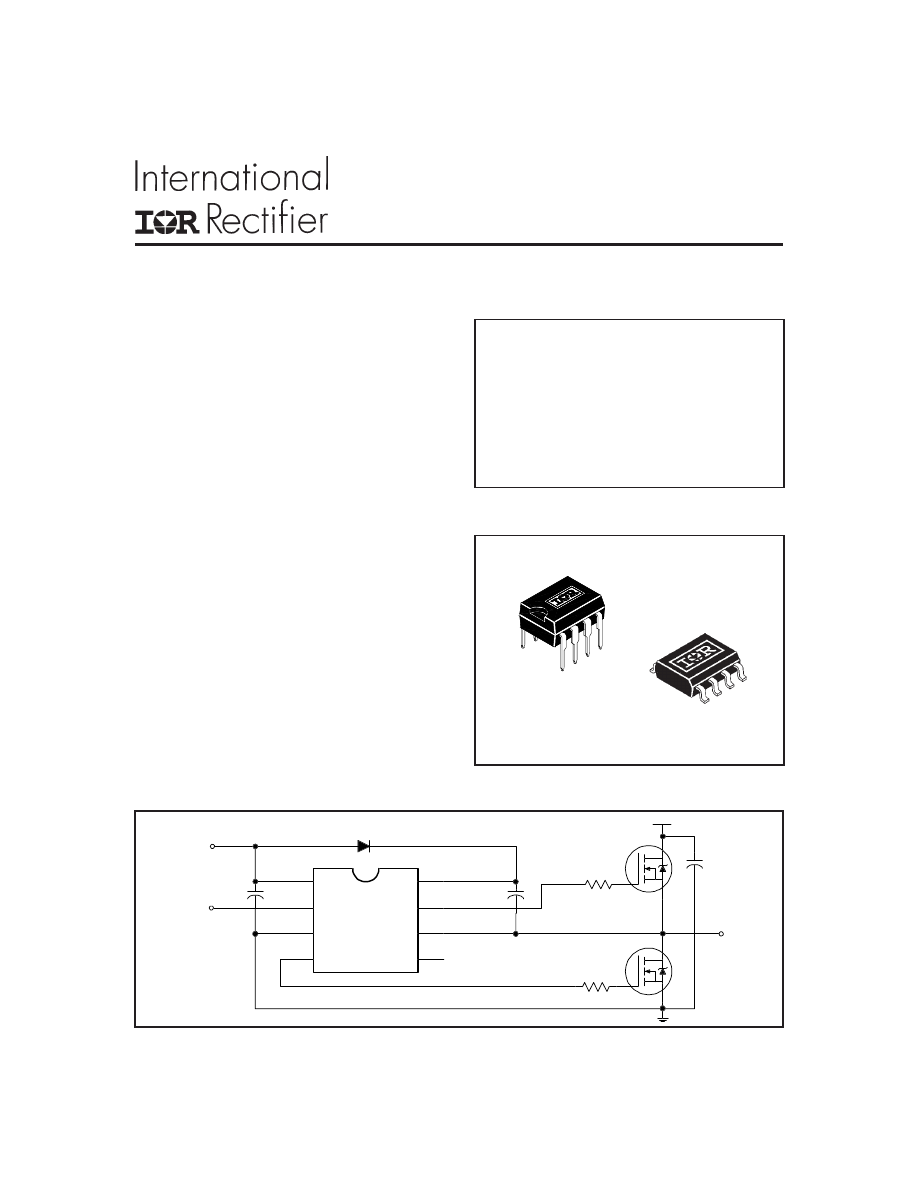
Typical Connection
Preliminary Data Sheet No. PD60028J
IR2111
HALF-BRIDGE DRIVER
Product Summary
V
OFFSET
600V max.
I
O
+/-
200 mA / 420 mA
V
OUT
10 - 20V
t
on/off
(typ.)
850 & 150 ns
Deadtime (typ.)
700 ns
Packages
V
CC
V
B
V
S
HO
LO
IN
COM
IN
up to 600V
TO
LOAD
V
CC
8 Lead PDIP
8 Lead SOIC
IR2111
2
Symbol Definition
Min.
Max.
Units
V
B
High side floating supply voltage
-0.3
625
V
S
High side floating supply offset voltage
V
B
- 25
V
B
+ 0.3
V
HO
High side floating output voltage
V
S
- 0.3
V
B
+ 0.3
V
CC
Low side and logic fixed supply voltage
-0.3
25
V
LO
Low side output voltage
-0.3
V
CC
+ 0.3
V
IN
Logic input voltage
-0.3
V
CC
+ 0.3
dV
s
/dt
Allowable offset supply voltage transient (figure 2)
—
50
V/ns
P
D
Package power dissipation @ T
A
≤
+25°C
(8 Lead DIP)
—
1.0
(8 lead SOIC)
—
0.625
Rth
JA
Thermal resistance, junction to ambient
(8 lead DIP)
—
125
(8 lead SOIC)
—
200
T
J
Junction temperature
—
150
T
S
Storage temperature
-55
150
T
L
Lead temperature (soldering, 10 seconds)
—
300
Absolute Maximum Ratings
Absolute maximum ratings indicate sustained limits beyond which damage to the device may occur. All voltage param-
eters are absolute voltages referenced to COM. The thermal resistance and power dissipation ratings are measured
under board mounted and still air conditions. Additional information is shown in figures 7 through 10.
V
W
°C/W
Symbol Definition
Min.
Max.
Units
V
B
High side floating supply absolute voltage
V
S
+ 10
V
S
+ 20
V
S
High side floating supply offset voltage
Note 1
600
V
HO
High side floating output voltage
V
S
V
B
V
CC
Low side and logic fixed supply voltage
10
20
V
LO
Low side output voltage
0
V
CC
V
IN
Logic input voltage
0
V
CC
T
A
Ambient temperature
-40
125
Note 1: Logic operational for V
S
of -5 to +600V. Logic state held for V
S
of -5V to -V
BS
.
Recommended Operating Conditions
The input/output logic timing diagram is shown in figure 1. For proper operation the device should be used within the
recommended conditions. The V
S
offset rating is tested with all supplies biased at 15V differential.
°C
V
°C
IR2111
3
Symbol
Definition
Min.
Typ. Max. Units Test Conditions
ton
Turn-on propagation delay
—
850
1,000
V
S
= 0V
toff
Turn-off propagation delay
—
150
180
V
S
= 600V
tr
Turn-on rise time
—
80
130
tf
Turn-off fall time
—
40
65
DT
Deadtime, LS turn-off to HS turn-on &
—
700
900
HS turn-off to LS turn-on
MT
Delay matching, HS & LS turn-on/off
—
30
—
Dynamic Electrical Characteristics
V
BIAS
(V
CC
, V
BS
) = 15V, C
L
= 1000 pF and T
A
= 25°C unless otherwise specified. The dynamic electrical characteristics
are measured using the test circuit shown in figure 3.
ns
Symbol
Definition
Min.
Typ. Max. Units Test Conditions
V
IH
Logic “1” input voltage for HO & logic “0” for LO
6.4
—
—
V
CC
= 10V
9.5
—
—
V
CC
= 15V
12.6
—
—
V
CC
= 20V
V
IL
Logic “0” input voltage for HO & logic “1” for LO
—
—
3.8
V
CC
= 10V
—
—
6.0
V
CC
= 15V
—
—
8.3
V
CC
= 20V
V
OH
High level output voltage, V
BIAS
- V
O
—
—
100
I
O
= 0A
V
OL
Low level output voltage, V
O
—
—
100
I
O
= 0A
I
LK
Offset supply leakage current
—
—
50
V
B
= V
S
= 600V
I
QBS
Quiescent V
BS
supply current
—
50
100
V
IN
= 0V or V
CC
I
QCC
Quiescent V
CC
supply current
—
70
180
V
IN
= 0V or V
CC
I
IN+
Logic “1” input bias current
—
20
40
V
IN
= V
CC
I
IN-
Logic “0” input bias current
—
—
1.0
V
IN
= 0V
V
BSUV+
V
BS
supply undervoltage positive going threshold
7.3
8.4
9.5
V
BSUV-
V
BS
supply undervoltage negative going threshold
7.0
8.1
9.2
V
CCUV+
V
CC
supply undervoltage positive going threshold
7.6
8.6
9.6
V
CCUV-
V
CC
supply undervoltage negative going threshold
7.2
8.2
9.2
I
O+
Output high short circuit pulsed current
200
250
—
V
O
= 0V, V
IN
= V
CC
PW
≤
10 µs
I
O-
Output low short circuit pulsed current
420
500
—
V
O
= 15V, V
IN
= 0V
PW
≤
10 µs
Static Electrical Characteristics
V
BIAS
(V
CC
, V
BS
) = 15V and T
A
= 25°C unless otherwise specified. The V
IN
, V
TH
and I
IN
parameters are referenced to
COM. The V
O
and I
O
parameters are referenced to COM and are applicable to the respective output leads: HO or LO.
mV
mA
V
V
µA
IR2111
4
Symbol Description
IN
Logic input for high side and low side gate driver outputs (HO & LO), in phase with HO
V
B
High side floating supply
HO
High side gate drive output
V
S
High side floating supply return
V
CC
Low side and logic fixed supply
LO
Low side gate drive output
COM
Low side return
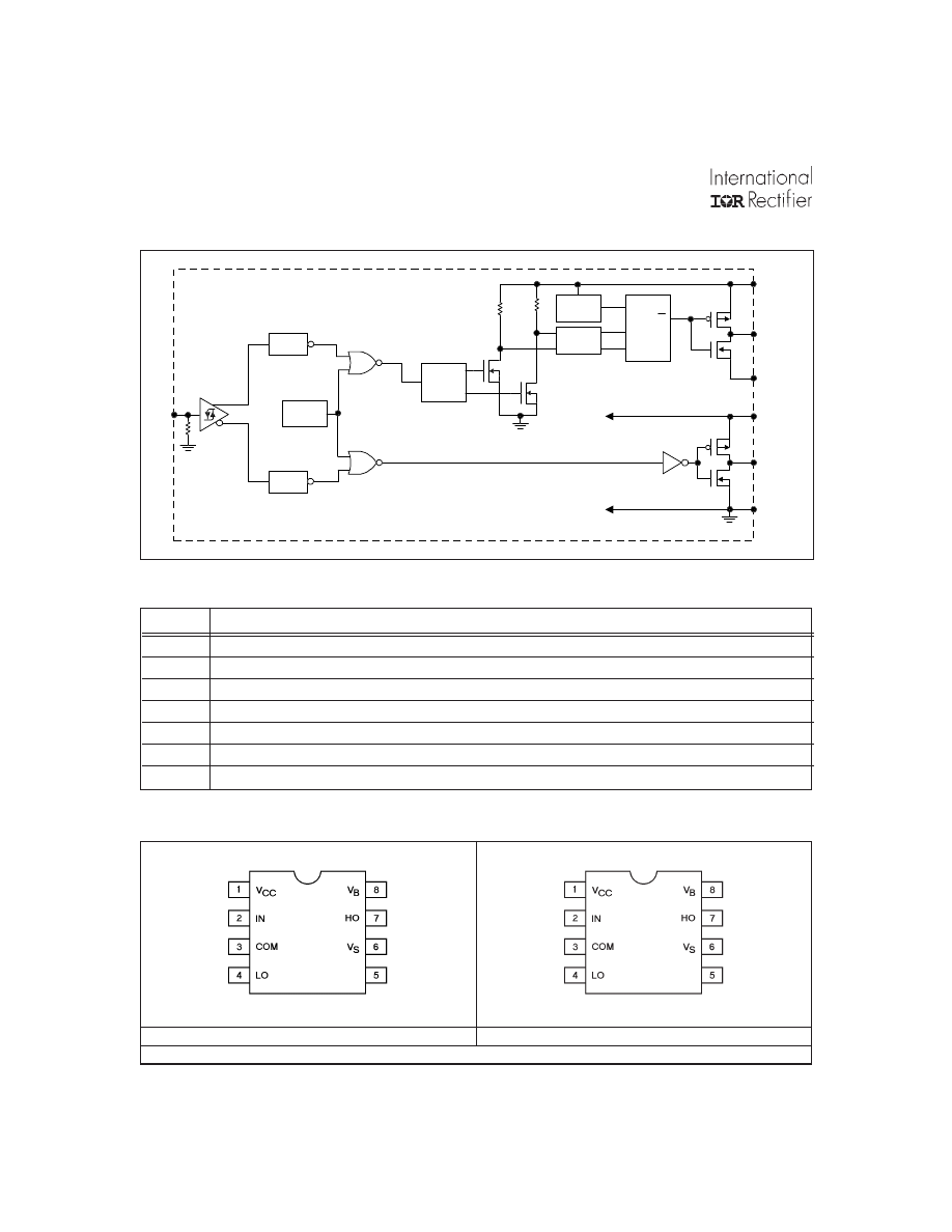
Functional Block Diagram
8 Lead DIP
8 Lead SOIC
IR2111
IR2111S
Part Number
Lead Assignments
PULSE
G E N
IN
UV
DETECT
C O M
H O
V
S
V
CC
L O
V
B
Q
S
R
R
PULSE
FILTER
HV
LEVEL
SHIFT
DEAD
TIME
DEAD
TIME
UV
DETECT
Lead Definitions
IR2111
5
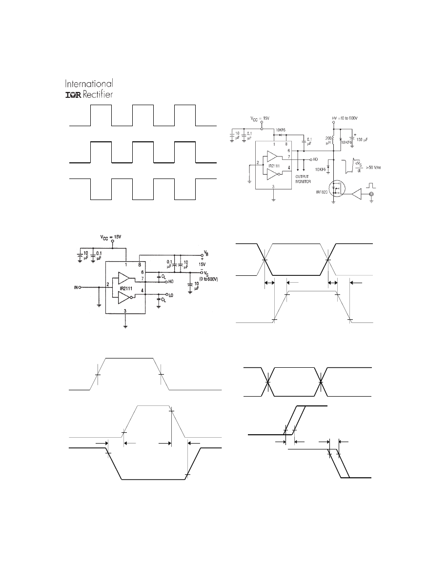
Figure 1. Input/Output Timing Diagram
Figure 2. Floating Supply Voltage Transient Test Circuit
Figure 3. Switching Time Test Circuit
Figure 4. Switching Time Waveform Definition
Figure 5. Deadtime Waveform Definitions
Figure 6. Delay Matching Waveform Definitions
HO
IN
LO
IN
(HO)
tr
ton
tf
toff
LO
HO
50%
50%
90%
90%
10%
10%
IN
(LO)
IN
HO
50%
50%
90%
10%
LO
90%
10%
DT
HO
50%
50%
10%
LO
90%
MT
HO
LO
MT
IN
(LO)
IN
(HO)
IR2111
6
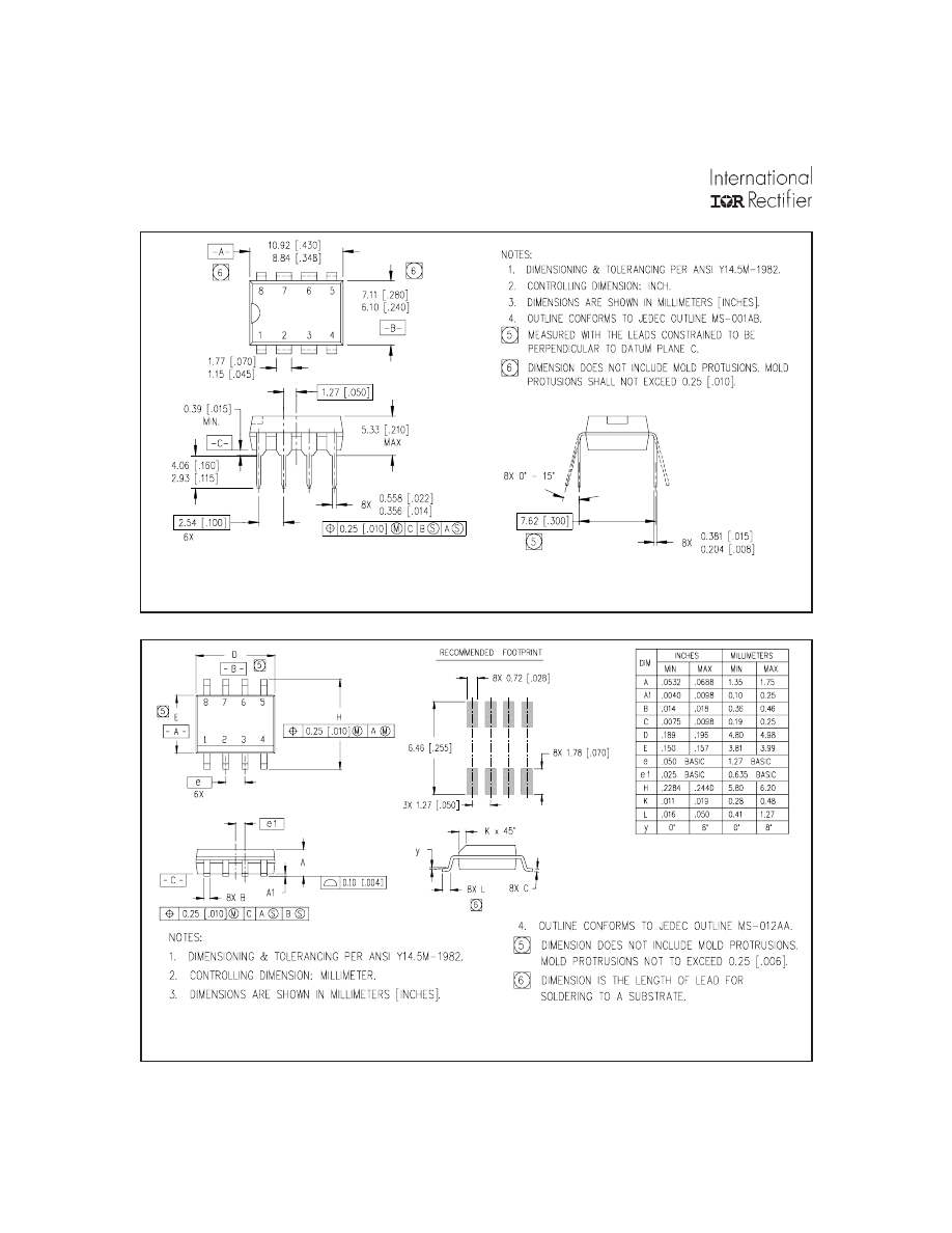
8 Lead PDIP
01-3003 01
8 Lead SOIC
01-0021 08
IR2111
7
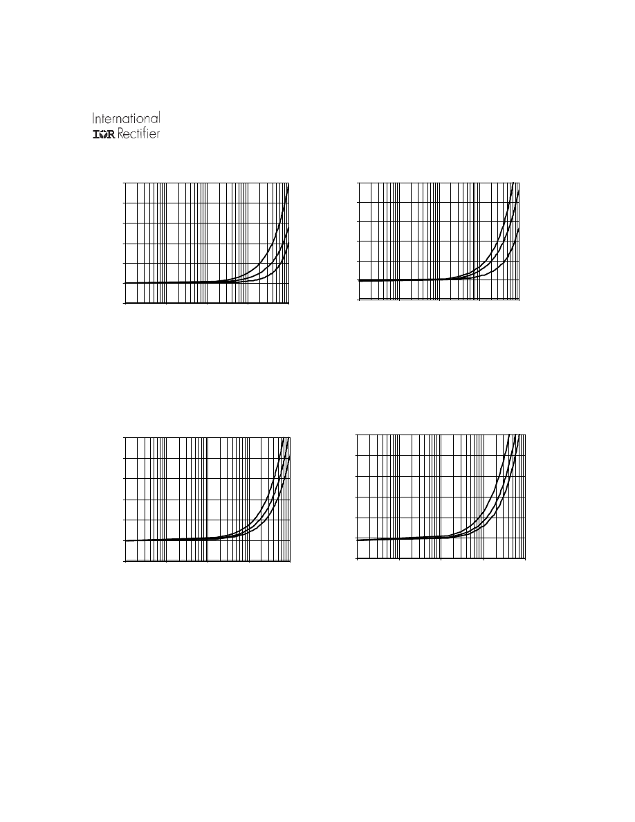
Frequency (Hz)
Figure 9. IR2111 T
J
vs. Frequency (IRFBC40)
R
GATE
= 15
Ω
Ω
Ω
Ω
Ω
, V
CC
= 15V
Frequency (Hz)
Figure 10. IR2111 T
J
vs. Frequency (IRFPC50)
R
GATE
= 10
Ω
Ω
Ω
Ω
Ω
, V
CC
= 15V
Frequency (Hz)
Figure 7. IR2111 T
J
vs. Frequency (IRFBC20)
R
GATE
= 33
Ω
Ω
Ω
Ω
Ω
, V
CC
= 15V
Frequency (Hz)
Figure 8. IR2111 T
J
vs. Frequency (IRFBC30)
R
GATE
= 22
Ω
Ω
Ω
Ω
Ω
, V
CC
= 15V
0
25
50
75
100
125
150
1E+2
1E+3
1E+4
1E+5
1E+6
Junc
ti
on Te
m
p
e
ra
ture
(
°C
)
320
160
30V
0
25
50
75
100
125
150
1E+2
1E+3
1E+4
1E+5
1E+6
Ju
nc
ti
on
Te
m
p
e
ra
tu
re
(
°C
)
320V
160V
30V
0
25
50
75
10 0
12 5
15 0
1E+2
1E+3
1E+4
1E+5
1E+6
Ju
n
ct
ion Te
m
p
e
ra
ture
(
°C
)
32 0V 16 0V
30 V
0
25
50
75
100
125
150
1E+2
1E+3
1E+4
1E+5
1E+6
Ju
nc
ti
on
T
e
m
p
e
ra
tu
re
(
°C
)
320V 160V 30V
IR2111
8
WORLD HEADQUARTERS: 233 Kansas St., El Segundo, California 90245 Tel: (310) 322 3331
IR GREAT BRITAIN: Hurst Green, Oxted, Surrey RH8 9BB, UK Tel: ++ 44 1883 732020
IR CANADA: 15 Lincoln Court, Brampton, Ontario L6T 3Z2 Tel: (905) 453-2200
IR GERMANY: Saalburgstrasse 157, 61350 Bad Homburg Tel: ++ 49 6172 96590
IR ITALY: Via Liguria 49, 10071 Borgaro, Torino Tel: ++ 39 11 451 0111
IR FAR EAST: K&H Bldg., 2F, 30-4 Nishi-Ikebukuro 3-Chome, Toshima-Ku, Tokyo, Japan 171 Tel: 81 3 3983 0086
IR SOUTHEAST ASIA: 1 Kim Seng Promenade, Great World City West Tower, 13-11, Singapore 237994 Tel: 65 838 4630
IR TAIWAN: 16 Fl. Suite D..207, Sec.2, Tun Haw South Road, Taipei, 10673, Taiwan Tel: 886-2-2377-9936
http://www.irf.com/
Data and specifications subject to change without notice. 3/1/99
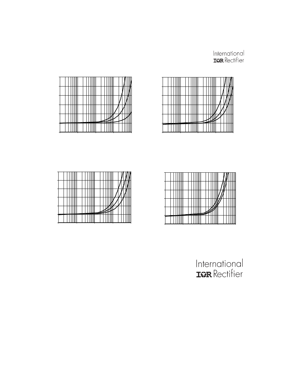
Frequency (Hz)
Figure 13. IR2111S T
J
vs. Frequency (IRFBC40)
R
GATE
= 15
Ω
Ω
Ω
Ω
Ω
, V
CC
= 15V
Frequency (Hz)
Figure 14. IR2111S T
J
vs. Frequency (IRFPC50)
R
GATE
= 10
Ω
Ω
Ω
Ω
Ω
, V
CC
= 15V
Frequency (Hz)
Figure 11. IR2111S T
J
vs. Frequency (IRFBC20)
R
GATE
= 33
Ω
Ω
Ω
Ω
Ω
, V
CC
= 15V
Frequency (Hz)
Figure 12. IR2111S T
J
vs. Frequency (IRFBC30)
R
GATE
= 22
Ω
Ω
Ω
Ω
Ω
, V
CC
= 15V
0
25
50
75
100
125
150
1E+2
1E+3
1E+4
1E+5
1E+6
Ju
nc
ti
on
T
e
m
p
e
ra
tu
re
(
°C
)
320V
160
30V
0
25
50
75
100
125
150
1E+2
1E+3
1E+4
1E+5
1E+6
Ju
nc
ti
on
Te
m
p
e
ra
tu
re
(
°C
)
320V 140V
30V
0
25
50
75
100
125
150
1E+2
1E+3
1E+4
1E+5
1E+6
Ju
nc
ti
on
T
e
m
p
e
ra
tur
e
(
°C
)
320V 140V
30V
0
25
50
75
100
125
150
1E+2
1E+3
1E+4
1E+5
1E+6
Ju
nc
ti
on
T
e
m
p
e
ra
tur
e
(
°C
)
320V 140V 30V
Wyszukiwarka
Podobne podstrony:
87 1237 1248 Machinability and Tool Wear During the High Speed Milling of Some Hardened
An investigation of shock induced temperature rise and melting of bismuth using high speed optical p
antybiotyki High Speed Countercurrent
high speed usb pcb layout recom Nieznany
ADSL High Speed Internetzugang
Fotopolis pl High speed photography w warunkach domowych
DB Systems Super High Grade Pre amp and DB 4 Moving Coil Cartridge Pre Amp
High Speed Countercurrent Chromatography
CD74HCT86 High Speed CMOS Logic Quad 2 Input EXCLUSIVE OR Gate
High speed photography sound trigger ZPT
High Speed Photography, czyli j Nieznany
Lab1 High Speed Camera XS 3
DB Systems Super High Grade Pre amp and DB 4 Moving Coil Cartridge Pre Amp
Fast virus detection by using high speed time delay neural networks
więcej podobnych podstron