MP1527
2A, 1.3MHz
Step-Up Converter
MP1527 Rev 1.8_8/31/05
Monolithic Power Systems, Inc.
1
Monolithic Power Systems
General Description
The MP1527 is a 2A, fixed frequency step-up
converter in a tiny 16 lead QFN package. The
high 1.3MHz switching frequency allows for
smaller external components producing a
compact solution for medium-to-high current
step-up, flyback, and SEPIC applications.
The MP1527 regulates the output voltage up
to 25V at efficiency as high as 93%. Soft-start,
timer-latch fault circuitry, cycle-by-cycle current
limiting, and input undervoltage lockout
prevent overstressing or damage to external
circuitry at startup and output short-circuit
conditions. Fixed frequency operation eases
control of noise making the MP1527 optimal
for noise sensitive applications such as mobile
handsets and wireless LAN PC cards.
Current-mode regulation and external
compensation components allow the MP1527
control loop to be optimized over wide variety
of input voltage, output voltage and load
current conditions.
The MP1527 is offered in a tiny 4mm x 4mm
16 lead QFN and 14 lead TSSOP packages.
Features
2A Peak Current Limit
Internal 150m
Ω Power Switch
V
IN
Range of 2.6V to 25V
>93% Efficiency
Zero Current Shutdown Mode
Under Voltage Lockout Protection
Timer-Latch Fault Detection
Soft Start Operation
Thermal Shutdown
Tiny 4mm x 4mm 16 pin QFN Package
Evaluation Board Available
Applications
SOHO Routers, PCMCIA Cards, Mini PCI
Handheld Computers, PDAs
Cell Phones, Digital and Video Cameras
Small LCD Display
Ordering Information
Part Number
Package
Temperature
MP1527DR QFN16
(4x4)
-40
° to +85°C
MP1527DM TSSOP14 -40
° to +85°C
EV0034
MP1527DR Evaluation Board
∗ For Tape & Reel, add suffix –Z (e.g. MP1527DR–Z)
For Lead Free, add suffix –LF (e.g. MP1527DR–LF–Z)
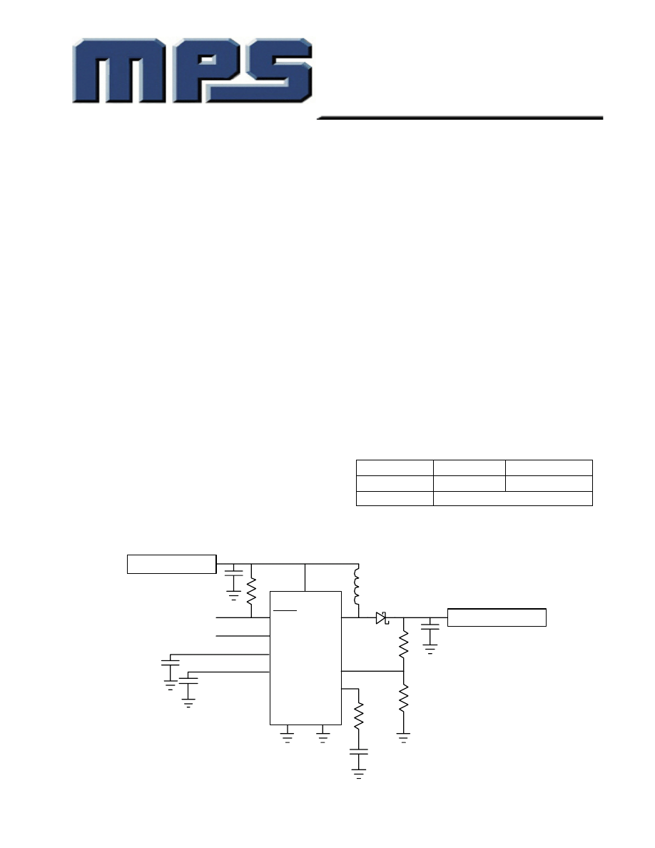
Figure 1: Typical Application Circuit
ON/OFF
FAULT
V
IN
= 2.6V to 25V
V
OUT
= 3.3V to 25V
SS
EN
FAULT
IN
BP
SGND
SW
FB
PGND
COMP

MP1527
2A, 1.3MHz
Step-Up Converter
MP1527 Rev 1.8_8/31/05
Monolithic Power Systems, Inc.
2
Monolithic Power Systems
Absolute Maximum Ratings (Note 1)
Input Supply Voltage
V
IN
-0.3V to 27V
SW Pin Voltage V
SW
-0.3V to 27V
Voltage at All Other Pins
-0.3V to 6V
Storage Temperature
-55
°C to +150°C
Recommended Operating Conditions
IN Input Supply Voltage V
IN
2.6V to 25V
Step Up Output Voltage
3.3V to 25V
Operating Temperature
-40
°C to +85°C
Package Thermal Characteristics
Thermal Resistance Θ
JA
(TSSOP14)
90°C/W
Thermal Resistance Θ
JA
(QFN16) (Note 2)
46°C/W
Electrical Characteristics
(V
IN
= 5.0V, T
A
= 25
°C unless specified otherwise)
Parameters Conditions
Min
Typ
Max
Units
IN Shutdown Supply Current
V
EN
<0.3V
0.5
1.0
µA
IN Operating Supply Current
V
EN
>2V, V
FB
=1.1V
0.9
1.2
mA
BP Output Voltage
V
IN
= 2.6V to 25V
2.4
V
IN Undervoltage Lockout Threshold
V
IN
Rising
2.1
2.4
V
IN Undervoltage Lockout Hysteresis
100
mV
EN Input Low Voltage
0.3
V
EN Input High Voltage
1.5
V
EN Input Hysteresis
100
mV
EN Input Bias Current
100
nA
SW Switching Frequency
1.0
1.3
1.5
MHz
SW Maximum Duty Cycle
V
FB
= 1.1V
85
90
%
Error Amplifier Voltage Gain
400
V/V
Error Amplifier Transconductance
300
µA/V
COMP Maximum Output Current
Sourcing and Sinking
30
µA
FB Regulation Threshold
1.196
1.22
1.244
V
FB Input Bias Current
V
FB
=1.22V
-100
nA
SS Charging Current
During Soft-Start
2
µA
FAULT Input Threshold Voltage
1.2
V
FAULT Output Low Voltage
V
FB
< 1.0V
0.2
V
V
IN
=5V
150
m
Ω
SW On Resistance
V
IN
=3V
225
m
Ω
SW Current Limit
(Note 3)
2.0
3.0
A
SW Leakage Current
V
SW
= 25V
0.5
µA
Thermal Shutdown
160
°C
Note 1: Exceeding these ratings may damage the device.
Note 2: Measured on approximately 1” square of 1oz copper.
Note 3: Guaranteed by design. Not tested.
MP1527
2A, 1.3MHz
Step-Up Converter
MP1527 Rev 1.8_8/31/05
Monolithic Power Systems, Inc.
3
Monolithic Power Systems
Pin Descriptions
COMP
NC
BP
EN
Top
View
PGND
PGND
SW
SW
SG
N
D
NC
NC
IN
FB
SS
F
AUL
T
SG
N
D
1
2
3
4
5
6
7
8
12
11
10
9
16
15
1
4
13
1
2
3
4
5
6
7
14
13
12
11
10
9
8
NC
NC
IN
SW
PGND
SGND
FAULT
SGND
EN
BP
NC
COMP
FB
SS
Table 1: Pin Description
QFN
Pin
TSSOP
Pin
Name Function
1 10
COMP
Compensation Node. COMP is the output of the internal transconductance error
amplifier. Connect a series RC network from COMP to SGND to compensate the
regulator control loop.
2, 6, 7
1, 2, 11
NC
No Connect
3 12 BP
Output of the internal 2.4V low dropout regulator. Connect a 10nF bypass
capacitor between BP and SGND. Do not apply an external load to BP.
4 13 EN
Regulator On/Off Control Input. A logic high input (V
EN
>1.5V) turns on the
regulator, a logic low puts the MP1527 into low current shutdown mode.
5, 13
6, 14
SGND
Signal Ground
8
3
IN
Input Supply
9, 10
4
SW
Output Switching Node. SW is the drain of the internal n-channel MOSFET.
Connect the inductor and rectifier to SW to complete the step-up converter.
11, 12
5
PGND
Power Ground
14 7
FAULT
Fault Input/Output.
FAULT
is an Input/Output that indicates that the MP1527
detected a fault and shuts the regulator off once a fault is indicated. Connect the
FAULT
input/outputs together for all MP1527 regulators to force all regulators off
when any one regulator detects a fault. Once a fault is detected, cycle EN or the
input power to restart the regulator. Pull
FAULT
to the input voltage through a
100kΩ resistor. Up to 20
FAULT
input/outputs can be connected in parallel.
15 8 SS
Soft-Start Input. Connect a 10nF to 22nF capacitor from SS to SGND to set the
soft-start and fault timer periods. SS sources 2
µA to an external soft-start
capacitor during start-up and when a fault is detected. As the voltage at SS
increases to 1.2V, the voltage at COMP is clamped to 0.7V above the voltage at
SS limiting the startup current. Under a fault condition, SS ramps at the same rate
as in soft-start. When the voltage at SS reaches 1.2V,
FAULT
is asserted and the
regulator is disabled. The external capacitor at SS is discharged to ground when
not in use or when under voltage lockout or thermal shutdown occurs.
16 9 FB
Regulation Feedback Input. Connect to external resistive voltage divider from the
output voltage to FB to set output voltage.
MP1527
2A, 1.3MHz
Step-Up Converter
MP1527 Rev 1.8_8/31/05
Monolithic Power Systems, Inc.
4
Monolithic Power Systems
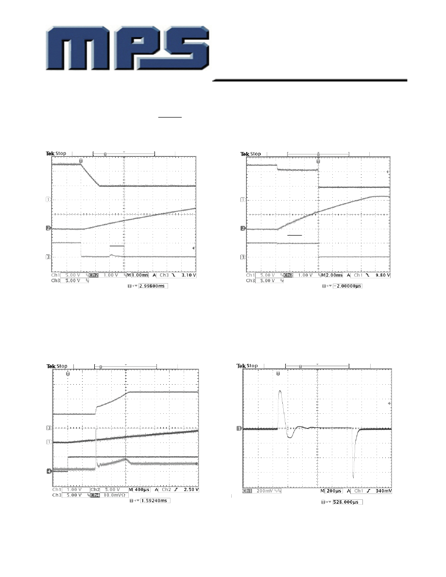
Typical Operating Characteristics
(Circuit of Figure 9: Unless Otherwise Specified)
Figure 2: MP1527 responding to FAULT being
Figure 3: MP1527 responding to an overload
driven low
V
OUT
V
SS
V
FAULT
V
OUT
V
SS
V
FAULT
Figure 4: MP1527 starting from EN being
Figure 5: Transient Load Response. Load
driven low-to-high
driven from 50mA to 500mA
V
OUT
V
SS
I
IN
(500mA/Div)
V
EN
V
OUT
MP1527
2A, 1.3MHz
Step-Up Converter
MP1527 Rev 1.8_8/31/05
Monolithic Power Systems, Inc.
5
Monolithic Power Systems
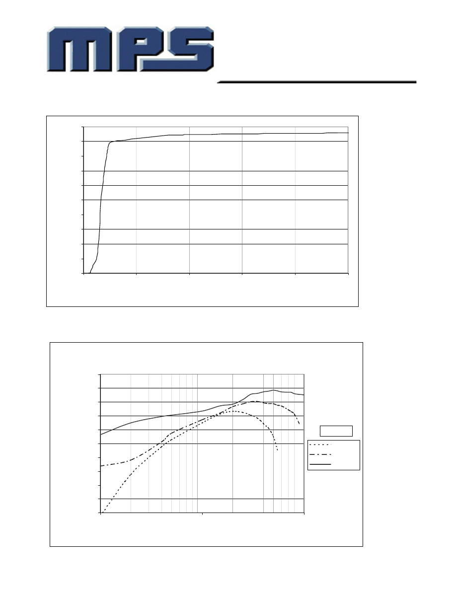
Figure 6: Quiescent Current versus Input Voltage (Bootstrapped)
0
100
200
300
400
500
600
700
800
900
1000
0
5
10
15
20
25
Input Voltage (V)
Qui
escent C
u
rrent (uA
)
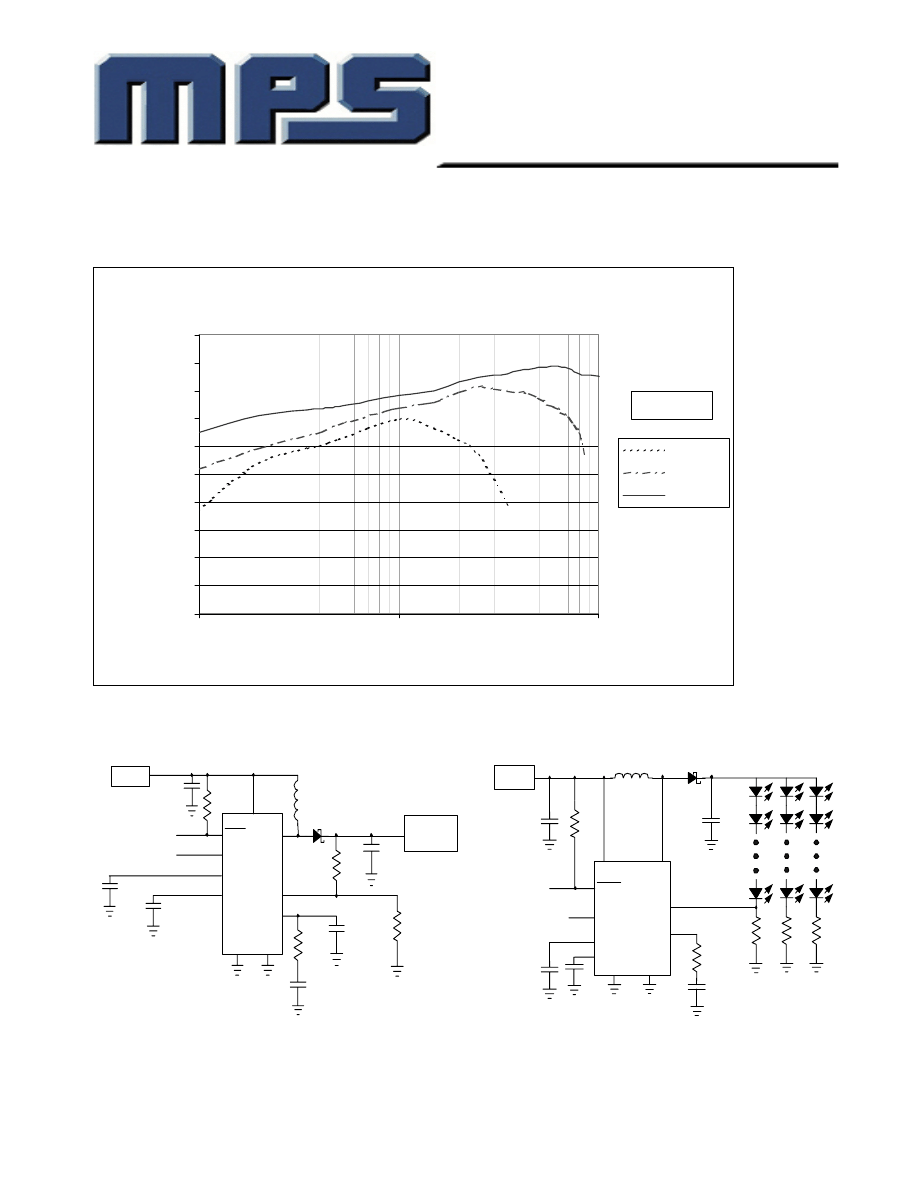
Figure 7: Efficiency vs. Load Current (Bootstrapped)
VOUT=12V
50.00%
55.00%
60.00%
65.00%
70.00%
75.00%
80.00%
85.00%
90.00%
95.00%
100.00%
10
100
1000
Load Current (mA)
Efficiency
VIN=3.3V
VIN=5V
VIN=8V
MP1527
2A, 1.3MHz
Step-Up Converter
MP1527 Rev 1.8_8/31/05
Monolithic Power Systems, Inc.
6
Monolithic Power Systems
Figure 8: Efficiency vs. Load Current (Non-Bootstrapped)
VOUT = 12V
50.00%
55.00%
60.00%
65.00%
70.00%
75.00%
80.00%
85.00%
90.00%
95.00%
100.00%
10
100
1000
Load Current (mA)
Efficien
cy
VIN=3.3V
VIN=5V
VIN=8V
Figure 9: V
IN
= 5V, V
OUT
= 12V @ 500mA Load
Figure 10: Driving Multiple Strings of White LEDs
ON/OFF
FAULT
V
IN
= 5V
V
OUT
= 12V
@ 0.5A
SS
EN
FAULT
IN
BP
SGND
SW
FB
PGND
COMP
10µF
C2
10µF
MBR0530
R3
10K
C3
5.6nF
10nF
10nF
4.7µH
10K
91K
100K
C4
N/A
ON/OFF
Up to
6 LEDs
per String
MP1527
IN
SS
EN
FB
SW
V
IN
=
2.6
to 25V
60
60
60
SGND
PGND
BP
FAULT
FAULT
COMP
4.7µF
1µF
1µF
10nF 10nF
5.6K
100K
4.7nF
1N5819H
W
MP1527
2A, 1.3MHz
Step-Up Converter
MP1527 Rev 1.8_8/31/05
Monolithic Power Systems, Inc.
7
Monolithic Power Systems
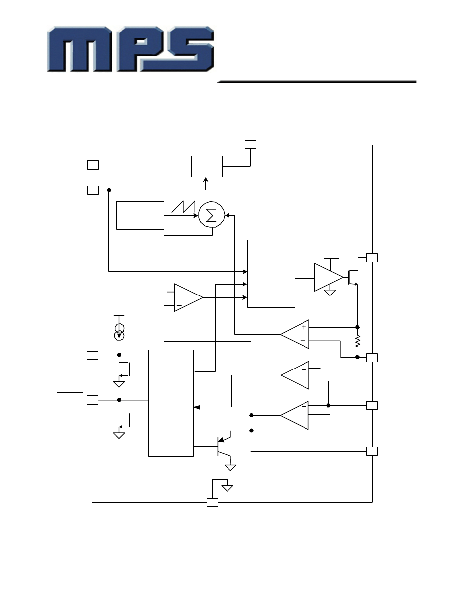
Figure 11: Functional Block Diagram
PWM
CONTROL
LOGIC
FAULT
SS
SGND
COMP
FB
1.22V
PGND
GM
SW
VDD
OSCILLATOR
LDO
EN
BP
2.4V
IN
2
µA
CURRENT
SENSE AMP
SOFT-
START
&
FAULT
CONTROL
1.098V

MP1527
2A, 1.3MHz
Step-Up Converter
MP1527 Rev 1.8_8/31/05
Monolithic Power Systems, Inc.
8
Monolithic Power Systems
Functional Description
The MP1527 uses a 1.3MHz fixed-frequency,
current-mode regulation architecture to
regulate the output voltage. The MP1527
measures the output voltage through an
external resistive voltage divider and compares
that to the internal 1.22V reference to generate
the error voltage at COMP. The current-mode
regulator compares voltage at the COMP pin
to the inductor current to regulate the output
voltage. The use of current-mode regulation
improves transient response and control loop
stability.
At the beginning of each cycle, the n-channel
MOSFET switch is turned on, forcing the
inductor current to rise. The current at the
source of the switch is internally measured and
converted to a voltage by the current sense
amplifier. That voltage is compared to the
error voltage at COMP. When the inductor
current rises sufficiently, the PWM comparator
turns off the switch forcing the inductor current
to the output capacitor through the external
rectifier. This forces the inductor current to
decrease. The peak inductor current is
controlled by the voltage at COMP, which in
turn is controlled by the output voltage. Thus
the output voltage controls the inductor current
to satisfy the load.
Internal Low-Dropout Regulator
The internal power to the MP1527 is supplied
from the input voltage (IN) through an internal
2.4V low-dropout linear regulator, whose
output is BP. Bypass BP to SGND with a 10nF
or greater capacitor to insure the MP1527
operates properly. The internal regulator can
not supply any more current than is required to
operate the MP1527, therefore do not apply
any external load to BP.
Soft-Start
The MP1527 includes a soft-start timer that
limits the voltage at COMP during start-up to
prevent excessive current at the input. This
prevents premature termination of the source
voltage at startup due to input current
overshoot at startup. When power is applied to
the MP1527, or with power applied when
enable is asserted, a 2µA internal current
source charges the external capacitor at SS.
As the capacitor charges, the voltage at SS
rises. The MP1527 internally clamps the
voltage at COMP to 0.7V above the voltage at
SS. This limits the inductor current at start-up,
forcing the input current to rise slowly to the
current required to regulate the output voltage
during soft-start.
The soft-start period is determined by the
equation:
t
SS
= 2.75 *10
5
* C
SS
Where C
SS
(in F) is the soft-start capacitor from
SS to SGND, and t
SS
(in seconds) is the soft-
start period.
Determine the capacitor required for a given
soft-start period by the equation:
C
SS
= 3.64 *10
-6
* t
SS
Use values for C
SS
between 10nF and 22nF to
set the soft-start period.
Fault Timer-Latch Function
The MP1527 includes an output fault detector
and timer-latch circuitry to disable the regulator
in the event of an undervoltage, overcurrent, or
thermal overload. Once the soft-start is
complete, the fault comparator monitors the
voltage at FB. If the voltage falls below the
1.098V fault threshold, the capacitor at SS
charges through an internal 2µA current
source. If the fault condition remains long
enough for the capacitor at SS to charge to
1.2V, the
FAULT
output is pulled low and the
power switch is turned off, disabling the output.

MP1527
2A, 1.3MHz
Step-Up Converter
MP1527 Rev 1.8_8/31/05
Monolithic Power Systems, Inc.
9
Monolithic Power Systems
The fault time-out period is determined by the
equation:
t
FAULT
= 6*10
5
* C
SS
If multiple MP1527 regulators are used in the
same circuit, the
FAULT
input/outputs can be
connected together. Should any one regulator
indicate a fault, it pulls all FAULT input/outputs
low, disabling all regulators. This insures that
all outputs are disabled should any one output
detect a fault. Pull-up
FAULT
to the input
voltage (IN) through a 100KΩ resistor. The
leakage current at
FAULT
is less than 250nA,
so up to 20
FAULT
input/outputs can be
connected together through a single 100KΩ
pull-up resistor. To reduce current draw when
FAULT
is active, a higher value pull-up resistor
may be used. Calculate the pull-up resistor
value by the equation:
100kΩ ≤ R
PULL-UP
≤ 2MΩ / N
Where N is the number of FAULT input/outputs
connected together.
Setting the Output Voltage
Set the output voltage by selecting the
resistive voltage divider ratio. The voltage
divider drops the output voltage to the 1.22V
feedback threshold voltage. Use 10KΩ for the
low-side resistor of the voltage divider.
Determine the high side resistor by the
equation:
R
H
= (V
OUT
- V
FB
) / (V
FB
/ R
L
)
where R
H
is the high-side resistor, R
L
is the
low-side resistor, V
OUT
is the output voltage
and V
FB
is the feedback regulation threshold.
For R
L
= 10KΩ and V
FB
= 1.22V, then
R
H
(KΩ) = 8.20* (V
OUT
– 1.22V)
Selecting the Input Capacitor
An input capacitor is required to supply the AC
ripple current to the inductor, while limiting
noise at the input source. A low ESR capacitor
is required to keep the noise at the IC to a
minimum. Ceramic capacitors are preferred,
but tantalum or low-ESR electrolytic capacitors
may also suffice.
Use an input capacitor value greater than
4.7µF. The capacitor can be electrolytic,
tantalum or ceramic. However since it absorbs
the input switching current it requires an
adequate ripple current rating. Use a capacitor
with RMS current rating greater than the
inductor ripple current (see Selecting The
Inductor to determine the inductor ripple
current).
To insure stable operation place the input
capacitor as close to the IC as possible.
Alternately a smaller high quality ceramic
0.1µF capacitor may be placed closer to the IC
with the larger capacitor placed further away. If
using this technique, it is recommended that
the larger capacitor be a tantalum or
electrolytic type. All ceramic capacitors should
be placed close to the MP1527.
Selecting the Output Capacitor
The output capacitor is required to maintain
the DC output voltage. Low ESR capacitors
are preferred to keep the output voltage ripple
to a minimum. The characteristic of the output
capacitor also affects the stability of the
regulation control system. Ceramic, tantalum,
or low ESR electrolytic capacitors are
recommended. In the case of ceramic
capacitors, the impedance of the capacitor at
the switching frequency is dominated by the
capacitance, and so the output voltage ripple is
mostly independent of the ESR. The output
voltage ripple is estimated to be:
SW
LOAD
OUT
IN
RIPPLE
f
2
C
I
V
V
-
1
V
×
×
⎟⎟
⎠
⎞
⎜⎜
⎝
⎛
≈
Where V
RIPPLE
is the output ripple voltage, V
IN
and V
OUT
are the DC input and output voltages
respectively, I
LOAD
is the load current, f
SW
is the
switching frequency, and C2 is the capacitance
of the output capacitor.
In the case of tantalum or low-ESR electrolytic
capacitors, the ESR dominates the impedance

MP1527
2A, 1.3MHz
Step-Up Converter
MP1527 Rev 1.8_8/31/05
Monolithic Power Systems, Inc.
10
Monolithic Power Systems
at the switching frequency, and so the output
ripple is calculated as:
IN
OUT
ESR
LOAD
SW
LOAD
OUT
IN
RIPPLE
V
V
R
I
f
2
C
I
)
V
V
1
(
V
×
×
+
×
×
−
≈
Where R
ESR
is the equivalent series resistance
of the output capacitors.
Choose an output capacitor to satisfy the
output ripple and load transient requirements
of the design. A 4.7µF-22µF ceramic capacitor
is suitable for most applications.
Selecting the Inductor
The inductor is required to force the higher
output voltage while being driven by the input
voltage. A larger value inductor results in less
ripple current that results in lower peak
inductor current, reducing stress on the
internal n-channel
.
switch. However, the larger
value inductor has a larger physical size,
higher series resistance, and/or lower
saturation current.
A 4.7µH inductor is recommended for most
applications. However, a more exact
inductance value can be calculated. A good
rule of thumb is to allow the peak-to-peak
ripple current to be approximately 30-50% of
the maximum input current. Make sure that the
peak inductor current is below 75% of the
current limit at the operating duty cycle to
prevent loss of regulation due to the current
limit. Also make sure that the inductor does not
saturate under the worst-case load transient
and startup conditions. Calculate the required
inductance value by the equation:
I
f
V
)
V
-
(V
V
L
SW
OUT
IN
OUT
IN
∆
×
×
=
×
η
×
×
=
IN
)
MAX
(
LOAD
OUT
)
MAX
(
IN
V
I
V
I
(
)
)
MAX
(
IN
I
%
50
%
30
I
−
=
∆
Where I
LOAD(MAX)
is the maximum load current, ∆I
is the peak-to-peak inductor ripple current, and η
is efficiency.
Selecting the Diode
The output rectifier diode supplies current to the
inductor when the internal MOSFET is off. To
reduce losses due to diode forward voltage and
recovery time, use a Schottky diode with the
MP1527. The diode should be rated for a
reverse voltage equal to or greater than the
output voltage used. The average current
rating must be greater than the maximum load
current expected, and the peak current rating
must be greater than the peak inductor current.
Compensation
The output of the transconductance error
amplifier (COMP) is used to compensate the
regulation control system. The system uses
two poles and one zero to stabilize the control
loop. The poles are f
P1
set by the output
capacitor and load resistance and f
P2
set by
the compensation capacitor C3. The zero f
Z1
is set by the compensation capacitor C3 and
the compensation resistor R3. These are
determined by the equations:
f
P1
= 1 / (π*C2*R
LOAD
)
f
P2
= G
EA
/ (2π*A
VEA
*C3)
f
Z1
= 1 / (2π*C3*R3)
Where R
LOAD
is the load resistance, G
EA
is the
error amplifier transconductance, and A
VEA
is
the error amplifier voltage gain.
The DC loop gain is:
A
VDC
= A
VEA
*G
CS
*(V
IN
/ V
OUT
)*R
LOAD
*(V
FB
/ V
OUT
)
or
A
VDC
= A
VEA
*G
CS
*V
IN
*V
FB
*R
LOAD
/(V
OUT
)
2
Where G
CS
is the current sense gain, V
IN
is the
input voltage, V
FB
is the feedback regulation
threshold, and V
OUT
is the regulated output
voltage.

MP1527
2A, 1.3MHz
Step-Up Converter
MP1527 Rev 1.8_8/31/05
Monolithic Power Systems, Inc.
11
Monolithic Power Systems
There is also a right-half-plane zero (f
RHPZ
) that
exists in all continuous mode (continuous
mode means that the inductor current does not
drop to zero on each cycle) step-up
converters. The frequency of the right half
plane zero is:
f
RHPZ
= V
IN
2
*R
LOAD
/ (2π*L*V
OUT
2
)
where L is the value of the inductor.
To stabilize the regulation control loop, the
crossover frequency (The frequency where the
loop gain drop to 0dB or gain of 1, indicated as
f
C
) should be at least one decade below the
right-half-plane zero and should be at most
75KHz. f
RHPZ
is at its lowest frequency at
maximum output load current (R
LOAD
is at a
minimum)
The crossover frequency is calculated by the
equation:
f
C
= A
VDC
*f
P1
*f
P2
/ f
Z1
or
f
C
= G
CS
*G
EA
*V
IN
*V
FB
*R3 / (2π*C2*V
OUT
2
)
The known values are:
G
CS
= 4.3S
G
EA
= 400µS
V
FB
= 1.22V
Putting in the known constants:
f
C
= 3.3x10
-4
*V
IN
*R3/ (C2*V
OUT
2
)
If the frequency of the right-half-pane zero
f
RHPZ
is less than 750KHz, then the crossover
frequency should be 1/10 of f
RHPZ
, and
determine the compensation resistor (R3) with
equation (1). If f
RHPZ
is greater than or equal to
750KHz, set the crossover frequency to 75KHz
with equation (2).
For f
C
= f
RHPZ
/ 10, then
R3 = V
IN
*R
LOAD-MIN
*C2 / (10G
CS
*G
EA
*V
FB
*L)
The minimum load resistance (R
LOAD-MIN
) is
equal to the regulated output voltage (V
OUT
)
divided by the maximum load current I
LOAD-MAX
.
Substituting that into the above equation:
R3 = V
IN
*V
OUT
*C2 /(10G
CS
*G
EA
*V
FB
*L*I
LOAD-MAX
)
Putting in the known constant values:
(1) R3 ≈ 48*V
IN
*V
OUT
*C2 / (L*I
LOAD-MAX
)
For f
C
= 75KHz,
f
C
= (G
CS
*G
EA
*V
IN
*V
FB
*R3) / (2π*C2*V
OUT
2
)
Solving for R3,
R3 = (2π*f
C
*C2*V
OUT
2
/ (G
CS
*G
EA
*V
IN
*V
FB
)
Using 75KHz for f
C
and putting in the other
known constants:
(
2) R3 ≈ 2.2x10
8
*C2*V
OUT
2
/ V
IN
The value of the compensation resistor is
limited to 10KΩ to prevent overshoot on the
output at turn-on. So if the value calculated for
R3 from either equation (1) or equation (2) is
greater than 10kΩ, use 10KΩ for R3.
Choose C3 to set the zero frequency f
Z1
to
one-fourth of the crossover frequency f
C
:
f
Z1
= f
C
/ 4
or
1 /(2π*C3*R3) = G
CS
*G
EA
*V
IN
*V
FB
*R3 / (8π*C2*V
OUT
2
)
Solving for C3:
C3 = 4*C2*V
OUT
2
/ (G
CS
*G
EA
*V
IN
*V
FB
*R3
2
)
Entering the known values gives:

MP1527
2A, 1.3MHz
Step-Up Converter
MP1527 Rev 1.8_8/31/05
Monolithic Power Systems, Inc.
12
Monolithic Power Systems
C3 ≈ 1.9x10
3
C2 V
OUT
2
/ (V
IN
R3
2
)
In some cases, if an output capacitor with high
capacitance and high equivalent series
resistance (ESR) is used, then a second
compensation capacitor (from COMP to
SGND) is required to compensate for the zero
introduced by the output capacitor ESR. The
extra capacitor is required if the ESR zero is
less than 4x the crossover frequency. The
ESR zero frequency is:
f
ZESR
= 1 / (2π*C2*R
ESR
)
The second compensation capacitor is
required if:
4*f
C
≥ f
ZESR
or
4*G
CS
*G
EA
*V
IN
*V
FB
*R3 / (2π*C2*V
OUT
2
)
≥ 1 /
(2π*C2*R
ESR
)
Simplifying:
(8.4x10
-3
*V
IN
*R3*R
ESR
)/ V
OUT
2
≥ 1
If this is the case, calculate the second
compensation capacitor by the equation:
R3*C4 = C2*R
ESR
or
C4 = (C2*R
ESR
) / R3
Example
Given:
Input Voltage (V
IN
): 5V
Output Voltage (V
OUT
): 12V
Maximum Load Current (I
LOAD-MAX
): 500mA
Output Capacitor (C2): 10µF (ESR=10mΩ
Maximum)
Inductor Value (L): 4.7µH
Find the frequency of the right-half-plane zero:
f
RHPZ
= V
IN
2
/ (2π*L*V
OUT
*I
LOAD-MAX
)
f
RHPZ
= (5V)
2
/
(2π*4.7µH*12V*500mA)=141KHz
The frequency of the right-half-plane zero is
less than 750khz, so use equation (1) to
determine the compensation resistor R3:
R3 ≈ 48*V
IN
*V
OUT
*C2 / (L*I
LOAD-MAX
)
R3 ≈ 48*5*12*10µF/(4.7µH*500mA) =12.3KΩ
(use 10KΩ)
Find the compensation capacitor C3:
C3 ≈ 1.9x10
3
*C2*V
OUT
2
/ (V
IN
*R3
2
)
C3 ≈ 1.9x10
3
*10µF (12V)
2
/ (5 * 10KΩ
2
) = 5.4nF
(use the nearest standard value, 5.6nF)
Determine if the second compensation
capacitor is required:
8.4x10
-3
* 5V * 5.6KΩ * 10mΩ / 12V
2
= 0.016 ≤ 1
Therefore no second compensation capacitor
is required.
MP1527
2A, 1.3MHz
Step-Up Converter
MP1527 Rev 1.8_8/31/05
Monolithic Power Systems, Inc.
13
Monolithic Power Systems
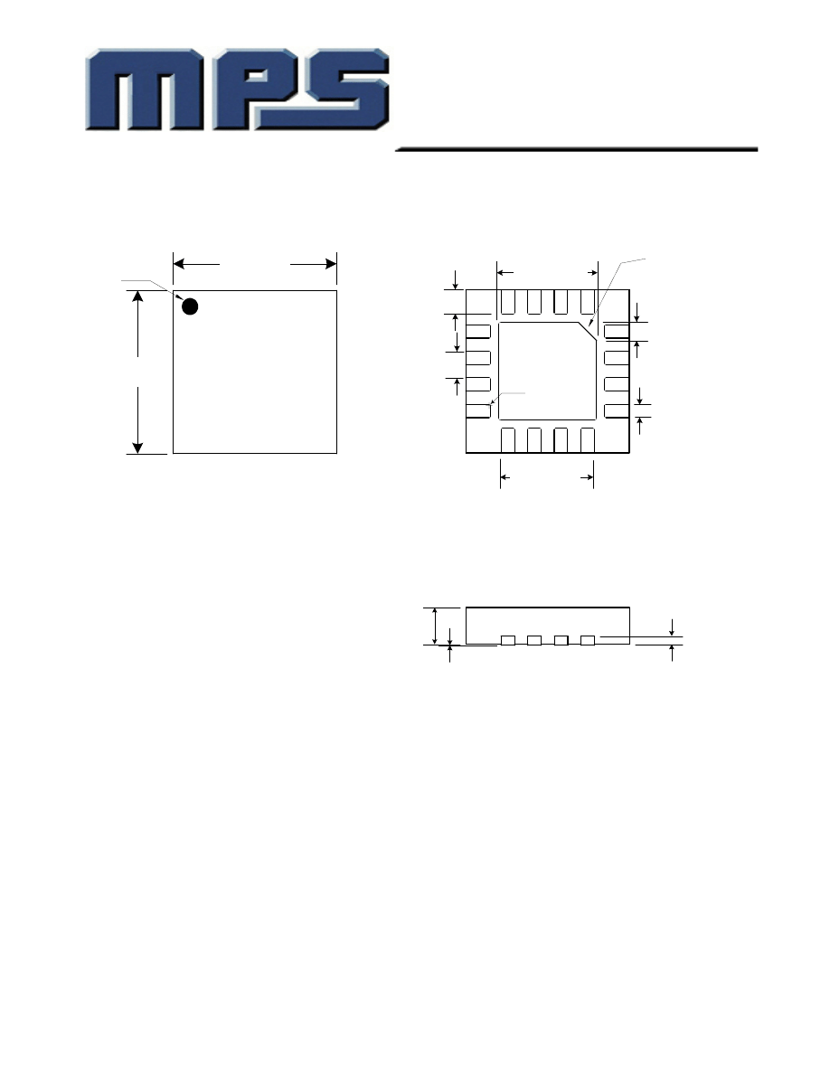
Packaging
QFN16 (4x4)
Pin 1 Identification
1
4
5
8
9
13
16
R0.030Max.
Side View
0.850 ( 0.0335)
0.950 (0.0374)
0.000-0.025
0.178 (0.007)
0.228 (0.009)
Btm View
Top View
3.950 (0.156)
4.050 (0.159)
3.950 (0.156)
4.050 (0.159)
Pin 1 Dot
By marking
(4 X 4mm)
QFN 16L
0.550 (0.217)
0.650 (0.256)
0.650
BSC
2.280 (0.898)
Ref.
0.40 (0.0158)
0.50 (0.0197)
2.35 (0.093)
2.45 (0.097)
0.28 (0.011)
0.38 (0.015)
MP1527
2A, 1.3MHz
Step-Up Converter
MP1527 Rev 1.8
Monolithic Power Systems, Inc.
14
8/31/05
983 University Ave, Building A, Los Gatos, CA 95032 USA
© 2003 MPS, Inc.
Tel: 408-357-6600
♦
Fax: 408-357-6601
♦
Web: www.monolithicpower.com
Monolithic Power Systems
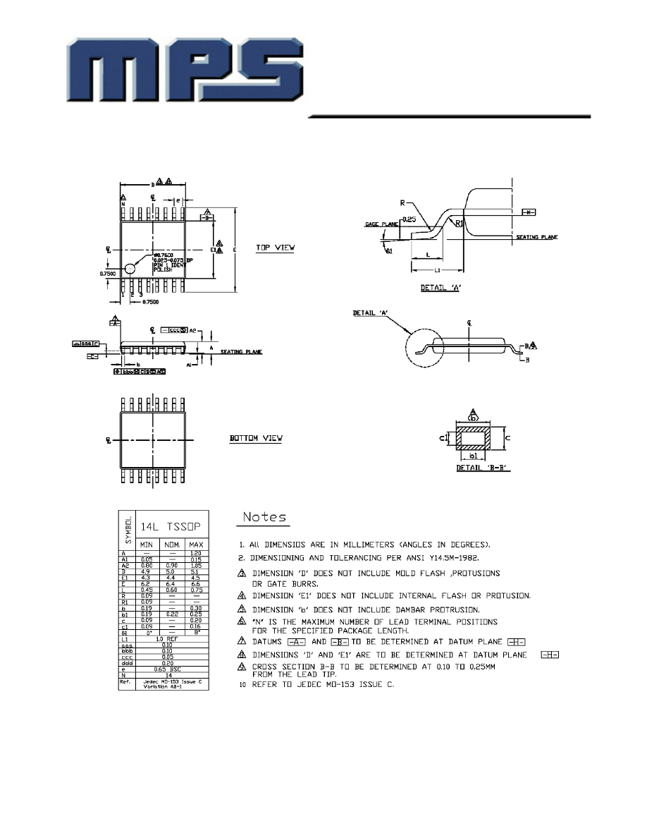
TSSOP14
NOTICE:
MPS believes the information in this document to be accurate and reliable. However, it is subject to change
without notice. Please contact the factory for current specifications. No responsibility is assumed by MPS for its use or fit to
any application, nor for infringement of patent or other rights of third parties.
Wyszukiwarka
Podobne podstrony:
strefy r1
R1 11
01kdpp r1 1
MP2305 r1 3
fema361 chap 5 r1
nierownosci R1
MP2307 r1 1
Ciagi liczbowe R1
MP2106 r1 3
2 letnie R1 godziny wbinp bid 2 Nieznany (2)
BROWN, R1,3
Marketing egzamin, ZiIP, ZiIP, R1, SII, marketing
Additional Affidavit R1
PIG-R1 2100, Rozdzial I.
ABS wersia D Cab r1 2[1]
r1
MP2104 r1 3
więcej podobnych podstron