MP2106
1.5A, 15V, 800KHz
Synchronous Buck Converter
MP2106 Rev. 1.3
www.MonolithicPower.com
1
9/26/2005
MPS Proprietary Information. Unauthorized Photocopy and Duplication Prohibited.
© 2005 MPS. All Rights Reserved.
The Future of Analog IC Technology
TM
TM
DESCRIPTION
The MP2106 is a 1.5A, 800KHz synchronous
buck converter designed for low voltage
applications requiring high efficiency. It is
capable of providing output voltages as low as
0.9V. MP2106 integrates top and bottom
switches to minimize power loss and
component count. The 800KHz switching
frequency reduces the size of filtering
components, further reducing the solution size.
The MP2106 includes cycle-by-cycle current
limiting and under voltage lockout. Internal
power switches, combined with the tiny 10-pin
MSOP or QFN packages, provide a solution
requiring a minimum of surface area.
EVALUATION BOARD REFERENCE
Board Number
Dimensions
EV2106DQ/DK-00A
2.5”X x 2.0”Y x 0.5”Z
FEATURES
• 1.5A Output Current
• Synchronous
Rectification
• Internal
210mΩ and 255mΩ Power Switches
• Input Range of 2.6V to 15V
• >90%
Efficiency
• Zero Current Shutdown Mode
• Under Voltage Lockout Protection
• Soft-Start
Operation
• Thermal
Shutdown
• Internal Current Limit (Source & Sink)
• Tiny 10-Pin MSOP or QFN Package
APPLICATIONS
• DC/DC Regulation from Wall Adapters
• Portable Entertainment Systems
• Set Top Boxes
• Digital Video Cameras, DECT
• Networking
Equipment
• Wireless
Modems
“MPS” and “The Future of Analog IC Technology” are Trademarks of Monolithic
Power Systems, Inc.
TYPICAL APPLICATION
MP2106
LX
VIN
BST
FB
6
7
8
2
9
10
4
3
1
5
COMP
SS
PGND
SGND
VREF
RUN
OUTPUT
1.8V / 1.5A
INPUT
2.6V to 15V
MP2106_TAC_S01
OFF ON
10nF
10nF
3.3nF
10nF
100
90
80
70
60
50
40
30
20
10
0
EFFICIENCY
(%)
0.01
0.1
1
10
LOAD CURRENT (A)
MP2106_TAC_EC02
Efficiency vs.
Load Current
V
IN
=5V
V
IN
=3.3V
MP2106 – 1.5A, 15V, 800KHz SYNCHRONOUS BUCK CONVERTER
MP2106 Rev. 1.3
www.MonolithicPower.com
2
9/26/2005
MPS Proprietary Information. Unauthorized Photocopy and Duplication Prohibited.
© 2005 MPS. All Rights Reserved.
TM
PACKAGE REFERENCE
SS
FB
COMP
VREF
RUN
1
2
3
4
5
10
9
8
7
6
SGND
PGND
LX
VIN
BST
TOP VIEW
MP2106_PD01-MSOP10
Part Number*
Package
Temperature
MP2106DK MSOP10 –40
°C to +85°C
*
For Tape & Reel, add suffix –Z (eg. MP2106DK–Z)
For Lead Free, add suffix –LF (eg. MP2106DK–LF–Z)
MP2106_PD02-QFN10
TOP VIEW
SS
FB
COMP
VREF
RUN
1
2
3
4
5
SGND
PGND
LX
VIN
BST
10
9
8
7
6
EXPOSED PAD
ON BACKSIDE
Part Number**
Package
Temperature
MP2106DQ
QFN10
(3mm x 3mm)
–40
°C to +85°C
**
For Tape & Reel, add suffix –Z (eg. MP2106DQ–Z)
For Lead Free, add suffix –LF (eg. MP2106DQ–LF–Z)
ABSOLUTE MAXIMUM RATINGS
(1)
Input Supply Voltage V
IN
.............................. 16V
LX Voltage V
LX
.....................
–
0.3V to V
IN
+ 0.3V
BST to LX Voltage .........................
–
0.3V to +6V
Voltage on All Other Pins...............
–
0.3V to +6V
Storage Temperature...............
–
55
°C to +150°C
Recommended Operating Conditions
(2)
Input Supply Voltage V
IN
..................2.6V to 15V
Output Voltage V
OUT
........................0.9V to 5.5V
Operating Temperature..............
–
40
°C to +85°C
Thermal Resistance
(3)
θ
JA
θ
JC
MSOP10 ................................ 150 ..... 65...
°C/W
QFN10 .................................... 50 ...... 12...
°C/W
Notes:
1) Exceeding
these
ratings may damage the device.
2) The device is not guaranteed to function outside of its
operating conditions.
3) Measured on approximately 1” square of 1 oz copper.
ELECTRICAL CHARACTERISTICS
V
IN
= 5.0V, T
A
= +25
°C, unless otherwise noted.
Parameter Symbol Condition
Min
Typ
Max
Units
Input Voltage Range
V
IN
2.6
15
V
Input Under Voltage Lockout
2.2
V
Input Under Voltage Lockout
Hysteresis
100 mV
Shutdown Supply Current
V
RUN
≤ 0.3V
0.5
1.0
µA
Operating Supply Current
V
RUN
> 2V, V
FB
= 1.1V
1.2
1.8
mA
VREF Voltage
V
REF
V
IN
= 2.6V to 15V
2.4
V
RUN Input Low Voltage
V
IL
0.4
V
RUN Input High Voltage
V
HL
1.5
V
RUN
Hysteresis
100 mV
RUN Input Bias Current
1
µA
Oscillator
Switching Frequency
f
SW
700 800 900 KHz
Maximum Duty Cycle
D
MAX
V
FB
= 0.7V
85
%
Minimum On Time
t
ON
200 ns
MP2106 – 1.5A, 15V, 800KHz SYNCHRONOUS BUCK CONVERTER
MP2106 Rev. 1.3
www.MonolithicPower.com
3
9/26/2005
MPS Proprietary Information. Unauthorized Photocopy and Duplication Prohibited.
© 2005 MPS. All Rights Reserved.
TM
ELECTRICAL CHARACTERISTICS
(continued)
V
IN
= 5.0V, T
A
= +25
°C, unless otherwise noted.
Parameter Symbol Condition
Min
Typ
Max
Units
Error Amplifier
Voltage Gain
A
VEA
400 V/V
Transconductance G
EA
300 µA/V
COMP Maximum Output Current
±30
µA
FB Regulation Voltage
V
FB
880 900 920 mV
FB Input Bias Current
I
FB
V
FB
= 0.9V
–100
nA
Soft-Start
Soft-start Current
I
SS
2 µA
Output Switch On-Resistance
V
IN
= 5V
255
mΩ
Switch On Resistance
V
IN
= 3V
315
mΩ
V
IN
= 5V
210
mΩ
Synchronous Rectifier On Resistance
V
IN
= 3V
255
mΩ
Switch Current Limit (Source)
2.5
A
Synchronous Rectifier Current Limit
(Sink)
350 mA
Thermal
Shutdown
160
°C
PIN FUNCTIONS
Pin #
Name
Description
1 SS
Soft-start Input. Place a capacitor from SS to SGND to set the soft-start period. The
MP2106 sources 2µA from SS to the soft-start capacitor at start up. As the voltage at SS
rises, the feedback threshold voltage increases to limit inrush current at startup.
2 FB
Feedback Input. FB is the inverting input of the internal error amplifier. Connect a resistive
voltage divider from the output voltage to FB to set the output voltage.
3 COMP
Compensation Node. COMP is the output of the error amplifier. Connect a series RC
network to compensate the regulation control loop.
4 VREF
Internal 2.4V Regulator Bypass. Connect a 10nF capacitor between VREF and SGND to
bypass the internal regulator. Do not apply any load to VREF.
5 RUN
On/Off Control Input. Drive RUN high to turn on the MP2106, drive RUN low to turn the
MP2106 off. For automatic startup, connect RUN to VIN via a pullup resistor.
6 BST
Power Switch Boost. BST powers the gate of the high-side N-Channel power MOSFET
switch. Connect a 10nF or greater capacitor between BST and LX.
7 VIN
Internal Power Input. VIN supplies the power to the MP2106 through the internal LDO
regulator. Bypass VIN to PGND with a 10µF or greater capacitor. Connect VIN to the input
source voltage.
8 LX
Output Switching Node. LX is the source of the high-side N-Channel switch and the drain
of the low-side N-Channel switch. Connect the output LC filter between LX and the output.
9 PGND
Power Ground. PGND is the source of the N-Channel MOSFET synchronous rectifier.
Connect PGND to SGND as close to the MP2106 as possible.
10 SGND
Signal
Ground.
MP2106 – 1.5A, 15V, 800KHz SYNCHRONOUS BUCK CONVERTER
MP2106 Rev. 1.3
www.MonolithicPower.com
4
9/26/2005
MPS Proprietary Information. Unauthorized Photocopy and Duplication Prohibited.
© 2005 MPS. All Rights Reserved.
TM
TYPICAL PERFORMANCE CHARACTERISTICS
Circuit of Figure 2, V
IN
= 5V, V
OUT
= 1.8V, L1 = 5µH, C1 = 10µF, C2 = 22µF, T
A
= +25
°C, unless
otherwise noted.
V
OUT
1V/div.
I
L
1A/div.
MP2106-TPC06
Short Circuit Protection
V
OUT
1V/div.
I
L
1A/div.
Short Circuit Recovery
MP2106-TPC07
V
SW
5V/div.
V
O
AC Coupled
10mV/div.
V
IN
AC Coupled
200mV/div.
I
L
1A/div.
MP2106-TPC01
Steady State Operation
1.5A Load
V
SW
5V/div.
V
O
AC Coupled
10mV/div.
V
IN
AC Coupled
20mV/div.
I
L
1A/div.
Steady State Operation
No Load
MP2106-TPC02
V
EN
2V/div.
V
OUT
1V/div.
V
SW
5V/div.
I
L
1A/div.
1ms/div.
MP2106-TPC04
Startup from Shutdown
1.5A Resistive Load
V
EN
2V/div.
V
OUT
1V/div.
V
SW
5V/div.
I
L
1A/div.
1ms/div.
Startup from Shutdown
No Load
MP2106-TPC05
V
OUT
AC Coupled
200mV/div.
I
LOAD
1A/div.
I
L
1A/div.
MP2106-TPC03
Load Transient
MP2106 – 1.5A, 15V, 800KHz SYNCHRONOUS BUCK CONVERTER
MP2106 Rev. 1.3
www.MonolithicPower.com
5
9/26/2005
MPS Proprietary Information. Unauthorized Photocopy and Duplication Prohibited.
© 2005 MPS. All Rights Reserved.
TM
OPERATION
MP2106_BD01
RUN
V
IN
7
6
8
9
2
3
10
1
4
5
FB
R2
R1
PGND
C7
C2
C1
LX
L1
V
REF
V
BP
2.4V
V
BP
V
IN
2.6V to 15V
SGND
V
OUT
OFF ON
800KHz
OSCILLATOR
RAMP
PWM
COMPARATOR
ENABLE
CKT & LDO
REGULATOR
GATE
DRIVE
REGULATOR
UVLO &
THERMAL
SHUTDOWN
CURRENT
LIMIT
COMPARATOR
CONTROL
LOGIC
--
+
Vdr
Vdr
Vdr
SS
C5
C6
V
FB
0.9V
GM
ERROR
AMPLIFIER
CURRENT
LIMIT
THRESHOLD
--
--
+
COMP
R3
C3
C4
--
--
+
+
CURRENT
SENSE
AMPLIFIER
--
+
BST
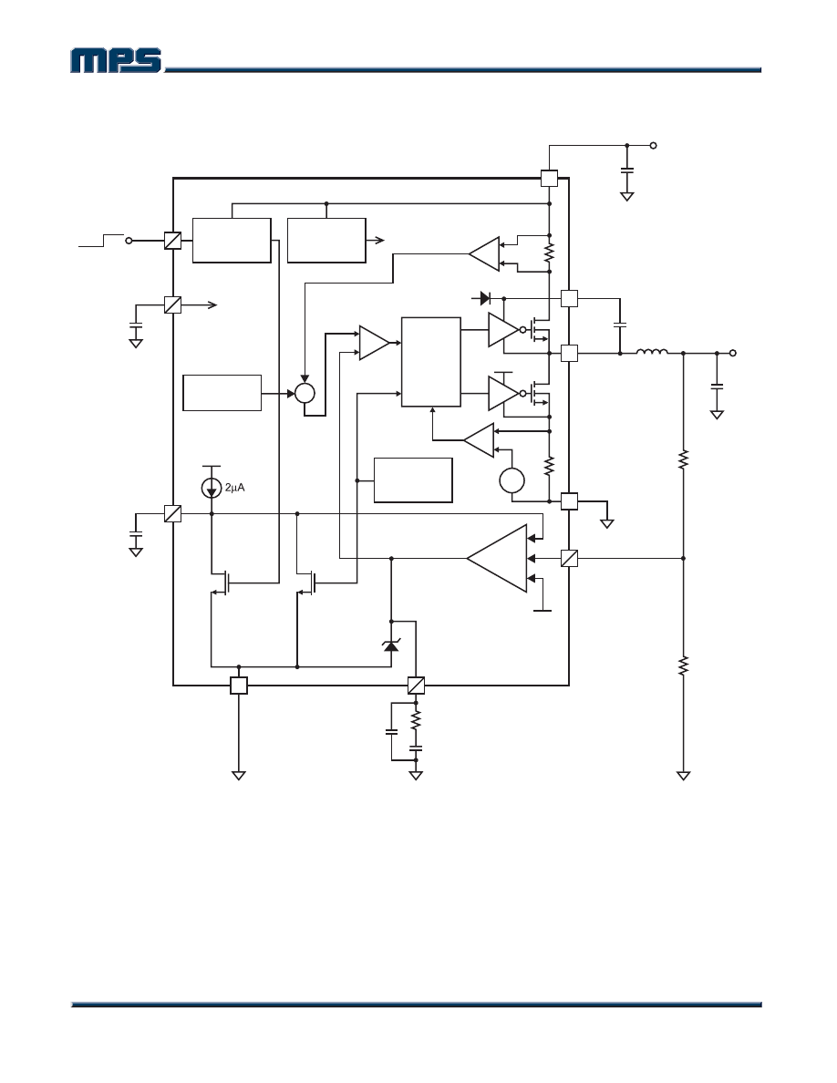
Figure 1—Functional Block Diagram
MP2106 – 1.5A, 15V, 800KHz SYNCHRONOUS BUCK CONVERTER
MP2106 Rev. 1.3
www.MonolithicPower.com
6
9/26/2005
MPS Proprietary Information. Unauthorized Photocopy and Duplication Prohibited.
© 2005 MPS. All Rights Reserved.
TM
The MP2106 measures the output voltage
through an external resistive voltage divider and
compares that to the internal 0.9V reference to
generate the error voltage at COMP. The
current-mode regulator uses the voltage at
COMP and compares it to the inductor current
to regulate the output voltage. The use of
current-mode regulation improves transient
response and improves control loop stability.
At the beginning of each cycle, the high-side
N-Channel MOSFET is turned on, forcing the
inductor current to rise. The current at the drain
of the high-side MOSFET is internally
measured and converted to a voltage by the
current sense amplifier.
That voltage is compared to the error voltage at
COMP. When the inductor current rises
sufficiently, the PWM comparator turns off the
high-side switch and turns on the low-side
switch, forcing the inductor current to decrease.
The average inductor current is controlled by
the voltage at COMP, which in turn, is
controlled by the output voltage. Thus the
output voltage controls the inductor current to
satisfy the load.
Since the high-side N-Channel MOSFET
requires voltage above V
IN
to drive its gate, a
bootstrap capacitor from LX to BST is required
to drive the high-side MOSFET gate. When LX
is driven low (through the low-side MOSFET),
the BST capacitor is internally charged. The
voltage at BST is applied to the high-side
MOSFET gate to turn it on, and maintains that
voltage until the high-side MOSFET is turned
off and the low-side MOSFET is turned on, and
the cycle repeats. Connect a 10nF or greater
capacitor from BST to SW to drive the high-side
MOSFET gate.
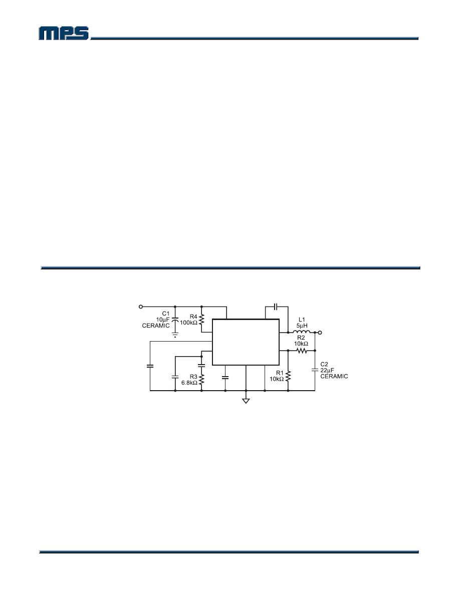
APPLICATION INFORMATION
MP2106
LX
VIN
BST
FB
COMP
SS
PGND
SGND
VREF
RUN
OUTPUT
1.8V / 1.5A
INPUT
2.6V to 15V
MP2106_TAC_F02
C5
10nF
C6
10nF
C3
3.3nF
C7
10nF
C4
OPEN
6
7
8
2
9
10
4
3
1
5
Figure 2—Typical Application Circuit
Internal Low-Dropout Regulator
The internal power to the MP2106 is supplied
from the input voltage (VIN) through an internal
2.4V low-dropout linear regulator, whose output
is VREF. Bypass VREF to SGND with a 10nF
or greater capacitor for proper operation. The
internal regulator can not supply more current
than is required to operate the MP2106.
Therefore, do not apply any external load to
VREF.
Soft-Start
The MP2106 includes a soft-start timer that
slowly ramps the output voltage at startup to
prevent excessive current at the input.
When power is applied to the MP2106, and
RUN is asserted, a 2µA internal current source
charges the external capacitor at SS. As the
capacitor charges, the voltage at SS rises. The
MP2106 internally limits the feedback threshold
voltage at FB to that of the voltage at SS. This
forces the output voltage to rise at the same
rate as the voltage at SS, forcing the output

MP2106 – 1.5A, 15V, 800KHz SYNCHRONOUS BUCK CONVERTER
MP2106 Rev. 1.3
www.MonolithicPower.com
7
9/26/2005
MPS Proprietary Information. Unauthorized Photocopy and Duplication Prohibited.
© 2005 MPS. All Rights Reserved.
TM
voltage to ramp linearly from 0V to the desired
regulation voltage during soft-start.
The soft-start period is determined by the
equation:
5
C
45
.
0
t
SS
×
=
Where C5
(in nF) is the soft-start capacitor from
SS to GND, and t
SS
(in ms) is the soft-start
period. Determine the capacitor required for a
given soft-start period by the equation:
SS
t
22
.
2
5
C
×
=
Use values for C5 between 10nF and 22nF to
set the soft-start period (between 4ms and
10ms).
Setting the Output Voltage (see Figure 2)
Set the output voltage by selecting the resistive
voltage divider ratio. The voltage divider drops
the output voltage to the 0.9V feedback voltage.
Use 10kΩ for the low-side resistor of the
voltage divider. Determine the high-side resistor
by the equation:
1
R
1
V
9
.
0
V
2
R
OUT
×
⎟⎟
⎠
⎞
⎜⎜
⎝
⎛
−
=
Where R2 is the high-side resistor, V
OUT
is the
output voltage and R1 is the low-side resistor.
Selecting the Input Capacitor
The input current to the step-down converter is
discontinuous, and so a capacitor is required to
supply the AC current to the step-down
converter while maintaining the DC input
voltage. A low ESR capacitor is required to
keep the noise at the IC to a minimum. Ceramic
capacitors are preferred, but tantalum or low
ESR electrolytic capacitors may also suffice.
The capacitor can be electrolytic, tantalum or
ceramic. Because it absorbs the input switching
current it must have an adequate ripple current
rating. Use a capacitor with RMS current rating
greater than 1/2 of the DC load current.
For stable operation, place the input capacitor
as close to the IC as possible. A smaller high
quality 0.1µF ceramic capacitor may be placed
closer to the IC with the larger capacitor placed
further away. If using this technique, it is
recommended that the larger capacitor be a
tantalum or electrolytic type. All ceramic
capacitors should be placed close to the
MP2106. For most applications, a 10µF ceramic
capacitor will work.
Selecting the Output Capacitor (C
OUT
)
The output capacitor is required to maintain the
DC output voltage. Low ESR capacitors are
preferred to keep the output voltage ripple to a
minimum. The characteristics of the output
capacitor also affect the stability of the
regulation control system. Ceramic, tantalum, or
low ESR electrolytic capacitors are
recommended.
The output voltage ripple is:
⎟⎟
⎠
⎞
⎜⎜
⎝
⎛
×
×
+
×
⎟⎟
⎠
⎞
⎜⎜
⎝
⎛
−
×
×
=
OUT
SW
ESR
IN
OUT
SW
OUT
RIPPLE
C
f
8
1
R
V
V
1
L
f
V
V
Where V
RIPPLE
is the output voltage ripple, f
SW
is
the switching frequency, V
IN
is the input voltage,
and R
ESR
is the equivalent series resistance of
the output capacitors and f
SW
is the switching
frequency.
Choose an output capacitor to satisfy the output
ripple requirements of the design. A 22µF
ceramic capacitor is suitable for most
applications.
Selecting the Inductor
The inductor is required to supply constant
current to the output load while being driven by
the switched input voltage. A larger value
inductor results in less ripple current that will
results in lower output ripple voltage. However,
the larger value inductor is likely to have a
larger physical size and higher series
resistance. Choose an inductor that does not
saturate under the worst-case load conditions.
A good rule for determining the inductance is to
allow the peak-to-peak ripple current to be
approximately 30% to 40% of the maximum
load current. Make sure that the peak inductor
current (the load current plus half the peak-to-
peak inductor ripple current) is below 2.5A to
prevent loss of regulation due to the current
limit.
MP2106 – 1.5A, 15V, 800KHz SYNCHRONOUS BUCK CONVERTER
MP2106 Rev. 1.3
www.MonolithicPower.com
8
9/26/2005
MPS Proprietary Information. Unauthorized Photocopy and Duplication Prohibited.
© 2005 MPS. All Rights Reserved.
TM
Calculate the required inductance value by the
equation:
(
)
I
f
V
V
V
V
L
SW
IN
OUT
IN
OUT
∆
×
×
−
×
=
Where ∆I is the peak-to-peak inductor ripple
current. It is recommended to choose ∆I to be
30%~40% of the maximum load current.
Compensation
The system stability is controlled through the
COMP pin. COMP is the output of the internal
transconductance error amplifier. A series
capacitor-resistor combination sets a pole-zero
combination to control the characteristics of the
control system.
The DC loop gain is:
LOAD
CS
VEA
OUT
FB
VDC
R
G
A
V
V
A
×
×
×
⎟⎟
⎠
⎞
⎜⎜
⎝
⎛
=
Where:
V
FB
is the feedback voltage, 0.9V, A
VEA
is the
transconductance error amplifier voltage gain,
400 V/V, G
CS
is the current sense
transconductance, (roughly the output current
divided by the voltage at COMP), 4.5A/V and
R
LOAD
is the load resistance:
OUT
OUT
LOAD
I
V
R
=
Where I
OUT
is the output load current.
The system has 2 poles of importance, one is
due to the compensation capacitor (C3), and
the other is due to the load resistance and the
output capacitor (C2), where:
3
C
A
2
G
f
VEA
EA
1
P
×
×
π
=
P1 is the first pole, and G
EA
is the error amplifier
transconductance (300µA/V) and
2
C
R
2
1
f
LOAD
2
P
×
×
π
=
The system has one zero of importance, due to
the compensation capacitor (C3) and the
compensation resistor (R3). The zero is:
3
C
3
R
2
1
f
1
Z
×
×
π
=
If large value capacitors with relatively high
equivalent-series-resistance (ESR) are used,
the zero due to the capacitance and ESR of the
output capacitor can be compensated by a third
pole set by R3 and C4. The pole is:
4
C
3
R
2
1
f
3
P
×
×
π
=
The system crossover frequency (the frequency
where the loop gain drops to 1, or 0dB) is
important. Set the crossover frequency to below
one tenth of the switching frequency to insure
stable operation. Lower crossover frequencies
result in slower response and worse transient
load recovery. Higher crossover frequencies
degrade the phase and/or gain margins and
can result in instability.
Table 1—Compensation Values for Typical
Output Voltage/Capacitor Combinations
V
OUT
C2 R3
C3
C4
1.8V 22µF Ceramic
6.8kΩ 3.3nF None
2.5V 22µF Ceramic
9.1kΩ 2.2nF None
3.3V 22µF Ceramic
12kΩ 1.8nF None
1.8V
47µF Tantalum
(300mΩ)
13kΩ 2nF 1nF
2.5V
47µF Tantalum
(300mΩ)
18kΩ 1.2nF
750pF
3.3V
47µF Tantalum
(300mΩ)
24kΩ 1nF
560pF
Choosing the Compensation Components
The values of the compensation components
given in Table 1 yields a stable control loop for
the output voltage and capacitor given. To
optimize the compensation components for
conditions not listed in Table 1, use the
following procedure.
MP2106 – 1.5A, 15V, 800KHz SYNCHRONOUS BUCK CONVERTER
MP2106 Rev. 1.3
www.MonolithicPower.com
9
9/26/2005
MPS Proprietary Information. Unauthorized Photocopy and Duplication Prohibited.
© 2005 MPS. All Rights Reserved.
TM
Choose the compensation resistor to set the
desired crossover frequency. Determine the
value by the following equation:
FB
CS
EA
C
OUT
V
G
G
f
V
2
C
2
3
R
×
×
×
×
×
π
=
Where f
C
is the desired crossover frequency
(preferably 33KHz).
Choose the compensation capacitor to set the
zero below one fourth of the crossover
frequency. Determine the value by the following
equation:
C
f
3
R
2
3
C
×
×
π
>
Determine if the second compensation
capacitor, C4 is required. It is required if the
ESR zero of the output capacitor happens at
less than half of the switching frequency. Or:
1
f
R
2
C
SW
ESR
>
×
×
×
π
If this is the case, then add the second
compensation capacitor.
Determine the value by the equation:
3
R
R
2
C
4
C
(max)
ESR
×
=
Where R
ESR(MAX)
is the maximum ESR of the
output capacitor.
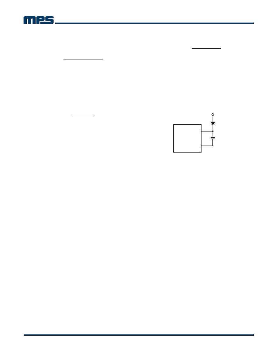
External Boost Diode
For 5V input or output applications, it is
recommended that an external boost diode be
added. This will help improve the regulator
efficiency. The diode can be a low cost diode
such as an IN4148 or BAT54.
MP2106
LX
BST
5V
8
6
BOOST
DIODE
10nF
MP2106_F03
Figure 3—External Boost Diode
MP2106 – 1.5A, 15V, 800KHz SYNCHRONOUS BUCK CONVERTER
NOTICE:
The information in this document is subject to change without notice. Please contact MPS for current specifications.
Users should warrant and guarantee that third party Intellectual Property rights are not infringed upon when integrating MPS
products into any application. MPS will not assume any legal responsibility for any said applications.
MP2106 Rev. 1.3
www.MonolithicPower.com
10
9/26/2005
MPS Proprietary Information. Unauthorized Photocopy and Duplication Prohibited.
© 2005 MPS. All Rights Reserved.
TM
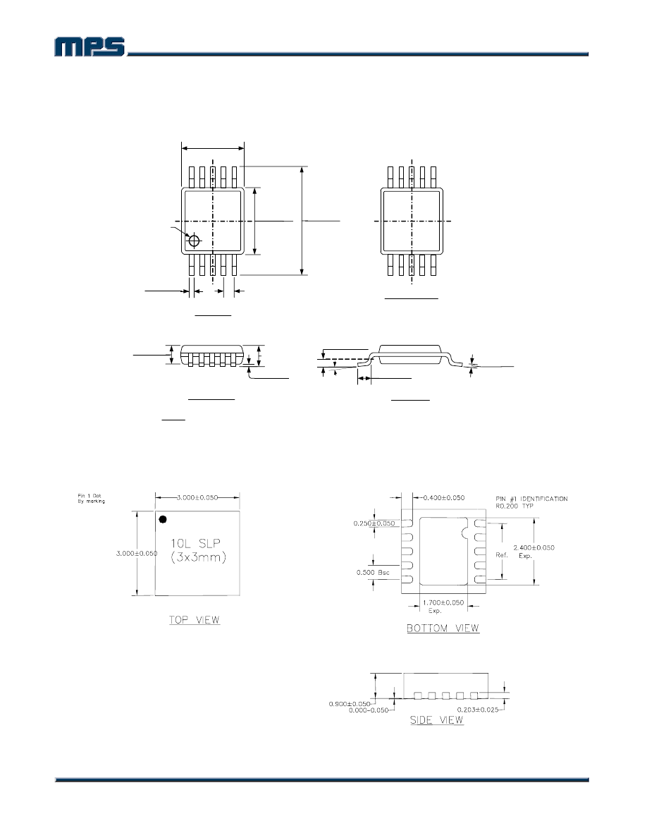
PACKAGE INFORMATION
MSOP10
BOTTOM VIEW
0.030(0.75)
0.037(0.95)
0.043(1.10)MAX
0.002(0.05)
0.006(0.15)
FRONT VIEW
0.004(0.10)
0.008(0.20)
SIDE VIEW
GAUGE PLANE
0.010(0.25)
0.016(0.40)
0.026(0.65)
0
o
-6
o
SEATING PLANE
PIN 1 ID
(NOTE 5)
0.114(2.90)
0.122(3.10)
0.187(4.75)
0.199(5.05)
1
5
6
10
0.007(0.18)
0.011(0.28)
0.0197(0.50)BSC
0.114(2.90)
0.122(3.10)
TOP VIEW
NOTE:
1) CONTROL DIMENSION IS IN INCHES. DIMENSION IN BRACKET IS IN MILLIMETERS.
QFN10 (3mm x 3mm)
2.250
PAD
PAD
Wyszukiwarka
Podobne podstrony:
strefy r1
R1 11
01kdpp r1 1
MP2305 r1 3
fema361 chap 5 r1
nierownosci R1
MP2307 r1 1
Ciagi liczbowe R1
MP1527 r1 8
2 letnie R1 godziny wbinp bid 2 Nieznany (2)
BROWN, R1,3
Marketing egzamin, ZiIP, ZiIP, R1, SII, marketing
Additional Affidavit R1
PIG-R1 2100, Rozdzial I.
ABS wersia D Cab r1 2[1]
r1
więcej podobnych podstron