
A Novel Multilevel Inverter Topology Based on
Multi-Winding Multi-Tapped Transformers for
Improved Wave Shape Requirements
E.S Deepak, C.S Anil, S Sanjay, C Febi and K.R Sajina,
Amrita VishwaVidyapeetham University
Abstract- The present work proposes a simple cost effective
multilevel topology for generating high quality sinusoidal AC
waveform based onmulti-tapped multi-winding transformer
switching technique. Multi-winding multi-tapped transformers
are used to aid the multi-level switching process which guarantees
a large number of intermediate switching levels. Each secondary
tapping can act as a separate DC source derived from the single
DC supply input to feed the second transformer. The proposed
topology can generate 27 switching states by using only 8 switches
and 3 full bridge diode rectifiers. The basic working principle is
based on the selective addition and subtraction of magnetic flux in
the transformer core. Although the mathematical modeling of
multi-winding multi-tapped transformer is slightly complex, the
resulting circuit complexity reduces when compared to the
conventional topologies like diode clamped, capacitor clamped
and cascaded multilevel inverters. The present work uses PSPICE
and MATLABmodeling techniques to simulate the entire system
using synthesized multi-winding multi-tapped transformer
models. Also the proposed system has superior quality
performance characteristics when compared to the conventional
topologies, due to its ability to avoid major drawbacks like
capacitor voltage unbalancing, common mode voltage stresses at
the load end and the requirement of large filters to avoid the
presence of harmonic frequencies at the output.
Index Terms- Multi-winding multi tapped transformer,
multilevel inverter, Common mode voltage, PSICE modeling
I.
I
NTRODUCTION
Multilevel inverter technology has become extremely
popular in recent years due to its increasing number of high
power applications such as large motor drives, flexible ac
transmission systems, power quality improvement devices and
renewable energy converters.
E.S. Deepak is with the Department of Electrical and Electronics
Engineering, Amrita University, Kollam, India (e-mail :
deepakes@gmail.com).
C.S. Anil (anil89cs@yahoo.com), S. Sanjay (sanjay.santhosh@gmail.com),
C. Febi (febichellampillai@gmail.com) and K.R. Sajina
(kr.sajina@gmail.com) are Electrical Engineering students (2007 to 2011
batch) at Amrita University, Kollam, India
978-1-4244-7882-8/11/$26.00
©2011
IEEE
Unlike normal voltage source inverters, multilevel inverters
provide several intermediate voltage levels which guarantee an
improved output voltage waveform as well as a less distorted
input current wave shape [2].The other features include large
power conversion capability, better harmonic spectrum, and
low dv/dt stress on switches, reduced EMI, lower switching
losses and smaller common mode voltage. They can also
operate at both fundamental switching frequency and higher
switching frequencies according to the applications [1].
The basic multilevel inverter topologies are diode clamped,
cascaded and capacitor clamped. Although the three topologies
provide multilevel operation, their disadvantages limit their
applications. Voltage unbalancing and unequal current stresses
are the major difficulties of diode clamped multilevel inverter.
Also, the number of clamping diodes required is quadratically
related to the number of levels which can be cumbersome for
units with high number of levels. In capacitor clamped, the
control is complicated to uphold the voltage levels for each of
the capacitors. The pre-charging of capacitors to the
corresponding voltages and the startup are also complex.For
lower switching frequency the clamping capacitoris larger in
size, decreasing the power density of the multilevel inverter
[1]. Switching utilization and efficiency are also poor for real
power transmission. The use of large number of capacitors is
more expensive and bulkier than clamping diodes. The main
disadvantage of cascaded cell multilevel inverter is the need of
separate DC sources for each of the H-bridges.
The number of isolated DC-links is more for a multilevel
inverter when compared to a two level inverter. The problems
caused by the neutral point voltage variations also make the
multilevel topology more complex. The power bus structure
and hence the control schemes become complicated as the
number of levels increases.
The present work focuses on a new multilevel inverter
topology utilizing the multi-winding multi-tapped transformer
structure to make a large number of output voltage levels with
minimum number of switches. The initial phase of the work
includes the study of conventional topologies through PSPICE
and MATLAB basedsimulations [6] and the second phase
proposes a new multilevel inverter topology. The proposed
topology can efficiently eliminate the main drawbacks of
conventional topologies and it can provide improved output
voltage wave shape.
II.
C
OMMON
M
ULTILEVEL
T
OPOLOGIES
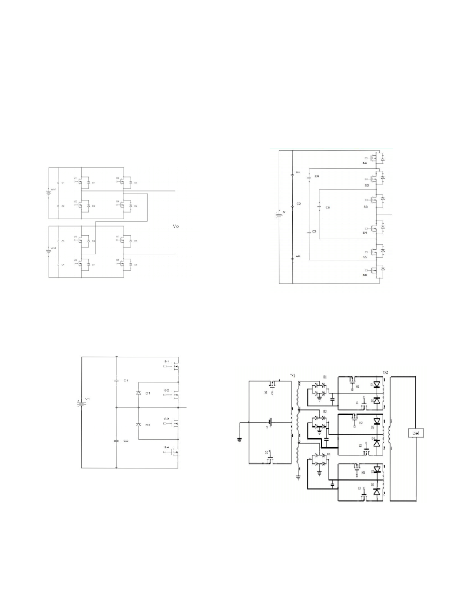
In cascaded multilevel inverter topology [3], each separate
DC source is connectedtodifferent H-bridge stages. Each H-
Bridge can generate three different voltage levels +V
DC
,0,-V
DC.
The number of output voltage levels in a cascaded inverter is
given by m=2s+1, where‘s’ is the number of separate dc
sources. Figure 1 shows the typical cascaded multilevel
inverter topology.
In Diode-clamped multilevel inverter [3], all the phases
share a common dc bus, which minimizes the capacitance
requirements. The voltage stress across each switching device
is limited to V
DC
through the clamping diodes.
Fig. 1. Cascaded Multilevel Topology
The number of diodes required for each phase is (m-1)*(m-
2), where ‘m’ is the number of required levels. The efficiency
of diode clamped inverter is high for fundamental switching
frequency.In the absence of precise monitoring and control, the
system will tend to overcharge or discharge the intermediate dc
levels. Figure 2 shows the typical diode clamped inverter [7].
Fig. 2. Diode Clamped Multilevel Topology
In capacitor clamped (flying-capacitor)multilevelinverter
[3], multiple capacitors are used to limit the voltage stress
across each switching device. This topology uses a ladder
structure of capacitors as shown in Figure 3, where the voltage
on each capacitor differs from that of the next capacitor.
One major advantage of the flying–capacitor based inverter
is that it provides redundancies for inner voltage levels. The
system requires (m-1)*(m-2)/2 auxiliary capacitors per phase if
the voltage rating of the capacitors is identical to the main
switches, in addition to (m-1) dc link capacitors. The use of
large number of capacitor makes the system more expensive
and bulky.
The current work reveals a new topology utilizing the
advantage of multi-winding multi tapped transformer and DC-
DC converter. In this topology, the number of switches, diodes
and capacitors required is very few. Diodes are used only for
rectification and freewheeling, and not for clamping.
Fig. 3. Flying Capacitor Topology
Using a single DC voltage source at the input, the system
derives several output voltage levels.
III.
T
HE
P
ROPOSED
S
YSTEM
Fig.4.The proposed multilevel inverter topology
A.
Description of the first stageinverter
The circuit diagram of the proposed multilevel topology is
shown in Figure 4. The main function of the first stage inverter
is to derive multiple DC levels at the secondary tappings from
a single DC supply input. The full bridge diode rectifier stage
acts as an interface between the first and the second stage
inverters.
B.
Description of the second stage inverter
The second stage inverter synthesizes twenty seven output
voltage levels from four DC input levels by selective addition
and subtraction of magnetic flux in the transformer core.The
full bridge rectifiers at the interface can act as separate DC
sources at the second stage inverter input.
C.
Role of capacitors and diodes in the circuit
Diodes are used in the circuit mainly for rectification and
freewheeling. The freewheeling diodes help to eliminate
switching spikes in the output waveform. The capacitor can not
only filter the first stage DC output, but it can also serve as DC
link to the second stage. The proposed topology can efficiently
minimize the voltage unbalance problem which is a common
issue in most of the conventional topologies.
D.
Embedded control system
Precise monitoring and control is a vital part of the inverter
operation. The real time control system for the proposed
topology can be implemented using an embedded controller.
All the switching strategy can be programmed into the
controller. Also the embedded controller can regulate the
output by generating compensatory gating pulses for the
switches. All the essential protective measures can be
incorporated with the embedded logic.
E.
Description of switching strategy
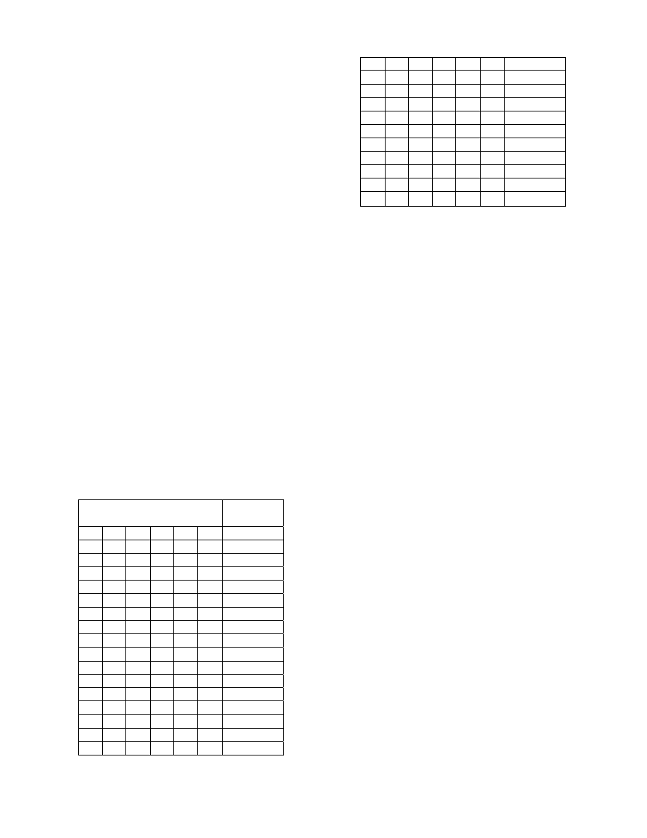
TABLE 1
SWITCHING STATES
VOLTAGE
LEVELS
H1 L1 H2 L2 H3 L3
0 1 0 1 0 1
-V
0 1 0 1 0 0 -12V/13
0 1 0 1 1 0 -11V/13
0 1 0 0 0 1 -10/13V
0 1 0 0 0 0 -9V/13
0 1 0 0 1 0 -8V/13
0 1 1 0 0 1 -7V/13
0 1 1 0 0 0 -6V/13
0 1 1 0 1 0 -5V/13
0 0 0 1 0 1 -4V/13
0 0 0 1 0 0 -3V/13
0 0 0 1 1 0 -2V/13
0 0 0 0 0 1 -V/13
0 0 0 0 0 0
0
0 0 0 0 1 0 +V/13
0 0 1 0 0 1 +2V/13
0 0 1 0 0 0 +3V/13
0 0 1 0 1 0 +4V/13
1 0 0 1 0 1 +5V/13
1 0 0 1 0 0 +6V/13
1 0 0 1 1 0 +7V/13
1 0 0 0 0 1 +8/13V
1 0 0 0 0 0 +9V/13V
1 0 0 0 1 0 +10V/13
1 0 1 0 0 1 +11V/13
1 0 1 0 0 0 +12V/13
1 0 1 0 1 0
+V
Even though the proposed system uses eight switches, the
output voltage levels are directly influenced only by the six
switches at the input of the second stage inverter. The required
levels are obtained by the selective addition and subtraction of
magnetic flux linked with the transformer core. This is
achieved by selecting the correct combination of switches. To
obtain the correct wave shape for the output voltage, it is
important to choose the switching sequence properly. Table 1
describes the switching strategy for the proposed system.
Using six switches at the input of the second stage inverter,
we obtain twenty seven voltage levels. Twenty seven switch
combinations are required to synthesize these twenty seven
output voltage levels. The switching states are as shown in
Table 1.
The outputs voltage levels of the three rectifier bridges are in
the ratio 9:3:1. This can be achieved by the proper design of
the first stage transformer. Various output voltage levels can be
synthesized by selecting switching combinations as described
below:
• For voltage level +V, switches H1,H2 and H3 are turned
on. The output of the bridges B1,B2 and B3 gets added up
(9+3+1).
• For voltage level +12V/13, the switches H1 and H2 are
turned on.The output of the bridge B1 which is 9V adds up
with the output of bridge B2 which is 3V to obtain +12V
(9+3).
• For voltage level +11V/13, the three switches H1,H2 and
L3 are turned on. The output of bridges B1 and B2 gets
added up while the output of bridge B3 gets subtracted
(9+3-1).
• For voltage level +10V/13, the switches H1and H3 are
turned on. The outputs of B1 and B3 gets added (9+1).
• For voltage level +9V/13, the switch H1 is turned on.
• For voltage level +8V/13, the switches H1 and L3 are
turned on. The output of B3 gets subtracted from the output
of B1 (9-1).
• For voltage level +7V/13, three switches H1,L2 and H3 are
turned on (9-3+1).
• For voltage level +6V/13, the switches H1 and L2 are
turned on (9-3).
• For voltage level +5V/13, three switches H1,L2 and L3(9-
3-1).
• For voltage level +4V/13, the switches H2and H3 are
turned on (3+1).
• For voltage level +3V/13, the switch H2 is turned on.
• For voltage level +2V/13, the switches H1 and L3 are
turned on (3-1).
• For voltage level +1V/13, the switchH3 are turned on.
• For voltage level 0, all the seven switches are turned off.
Similar is the case for negative voltage levels.
F.
Standalone Second Stage Inverter Application
The second stage inverter of the proposed topology can act
as a standalone multilevel inverter with isolated multiple dc
sources. Thus the topology is well suited for renewable power
conversion applications such as solar and wind based systems
provided the same 9:3:1input dc source voltage ratio is
maintained properly. The simulation results presented in the
following section is also valid for the standalone topology.
IV.
S
IMULATION
R
ESULTS
F
IG
.
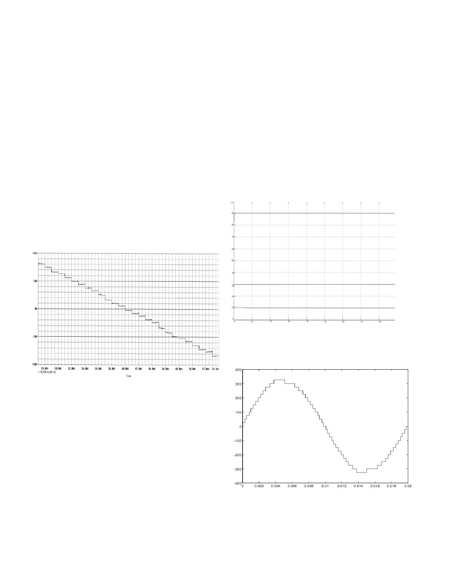
7
PSPICE Simulation Result- Unfiltered waveform
A.
PSPICE Simulation
The operation of the proposed topology is tested in PSPICE
and the output obtained is shown in figure7.It shows an
unfiltered staircase waveform with 27 voltage levels. Since
PSPICE does not include any templates for the multi-winding
multi-tapped transformer by default, derived models are
synthesized from the available basic models. Also the
unavailability of state machines in default PSPICE library can
make the simulation tedious. So the PSPICE simulation is used
for testing the peak to peak 27voltage level switching sequence
over a period of 180
o
as shown in figure 7. The complete
switching strategy is tested using MATLAB SIMULINK
[8],[9].
B.
MATLAB simulation
In order to perform a more detailed evaluationof the
proposed multilevel inverter system, MATLABis used. The
complete topology is modeled using SIMULINK toolbox and
the control logic is tested. Figure 8 shows thedc output
obtained from the first stage convertor which ensures 9:3:1
input voltage ratios for feeding the second stage. The filter
capacitors of the first stage can ensure stable dc input supplies
for the second stage.
The final output waveform of the second stage is a 27 level
staircase waveform as shown in figure 9. For a purely resistive
load the shape of the current waveform is exactly similar to the
voltage waveform. As the load becomes inductive the staircase
current waveform takes the shape of a sinusoidal wave. The
Fourier analysis of the voltage and current waveforms at the
output of the system shows a low THD of 3.99%. The quality
of the output wave shape can be significantly increased by
introducing proper pulse width modulation strategy along with
the switching scheme.
Fig. 8
MATLAB Simulation Results - First Stage Output
Fig. 9
MATLAB Simulation Results– Final Output

V.
A
DVANTAGES
A
ND
D
ISADVANTAGES
O
F
T
HE
P
ROPOSED
S
YSTEM
The proposed system uses only minimal number of switches
and capacitors. No clamping diodes are used in the system.
Unlike the other conventional topologies, the proposed
topology uses a only single DC source to synthesize output
voltage levels and the number of levels increases drastically by
increasing the number of windings in the transformer. The
design is made in such a way that the capacitors that are idle
during a switching period are continuously charged, thereby
reducing the capacitor voltage unbalancing problem to a
greater extend when compared to the conventional topologies.
Inspiteof these advantages, the use of transformers makes
the system bulky. Also the transformer design process makes
the system design tedious.
VI.
C
ONCLUSION
A wide range of modern high power applications demand a
high quality sinusoidal power supply. In order to satisfy the
requirement, multilevel inverter topologies are commonly
preferred. The demerits of the conventional topologies limit
their applications in various fields. The proposed topology can
efficiently minimize the main drawbacks of the conventional
topologies and it can provide a large number of output levels to
create a purely sinusoidal power supply. Even though the use
of multi-winding multi-tapped transformer increases the design
complexity of the topology, the resulting circuit is simple and
having minimum number of components. For the complete
development of the proposed system, more research needs to
be done in designing proper control strategy along with
suitable real-time embedded controller and multi-tapped multi-
winding transformers.
R
EFERENCES
[1] J. Rodriguez, J.S. Lai; F.Z. Peng, “Multilevel inverters:A
survey oftopologies, controls, and applications”, IEEE
Trans.on Industrial Electronics,vol.49, no.4, Aug. 2002, pp.
724-738.
[2]P.Panagis,F.Stergiopolos, P.Marabeas,
S.Manios.“Comparison of state of the art multilevel
inverters,”Power Electronics Specialists Conference PESC
2008,IEEE, 2008, pp. 4296-4301.
[3]R.W.Erickson,“Fundamentalsof Power
electronics,"Chapman and Hall ,May 1997.
[4]M.Wenzhong and K.L.L.Yaohua,“Research on a multilevel
high power converter,“IEEEInternational conference on
industrial application, vol. 1, 2004, pp. 341-344.
[5]E.Herbert, “Transformer SPICE model,” February 14, 2008.
[6]L.G.Meares and C.E. Hymowitz, “SPICE models for power
electronics,”.
[7]X.Yuan and I.Barbi,“Fundamentals of a new diode
Clamping Multilevel inverter,” IEEE Trans.onPower
Electronics, vol.15, No. 4, July 2000, pp. 711-718.
[8] Chin-Chiang Hua, Chu-Wei Wu and Chih-Wei Chuang,
“Fully digital control of 27-level cascade inverter with
variable DC voltage sources,”2007 Second IEEE Conference
on Industrial Electronics and Application
[9] F.S.Kang, S.J.Park, M.H.Lee and C.U.Kin, “An efficient
multilevel synthesis approach and its application to a 27 level
inverter,” IEEE Trans. on industrial electronics vol.52, no.6
,december 2005
Wyszukiwarka
Podobne podstrony:
A Novel Video Image Scaling Algorithm Based on Morphological Edge Interpolation
Multi Winding Transformer Based Diode Clamped Multi Level Inverter
A Trust System Based on Multi Level Virus Detection
Isolated Multi level Inverter Using 3 Phase Transformers
Implementation of a Mu;ti level Inverter Based on Selective Harmonic Elimination and Zig Zag Connect
Isolated Multi level Inverter Using 3 Phase Transformers
A Series Active Power Filter Based on a Sinusoidal Current Controlled Voltage Source Inverter
A New Low Cost Cc Pwm Inverter Based On Fuzzy Logic
A Series Active Power Filter Based on Sinusoidal Current Controlled Voltage Source Inverter
Performance Improvements in an arc welding power supply based on resonant inverters (1)
A New Low Cost Cc Pwm Inverter Based On Fuzzy Logic
A Series Active Power Filter Based on Sinusoidal Current Controlled Voltage Source Inverter
Design and construction of three phase transformer for a 1 kW multi level converter
Novel Techniques to Cancel Common mode Noise Based on Noise Balan
Electrochemical DNA biosensors based on platinum nanoparticles combined carbon nanotubes
Fundamnentals of dosimetry based on absorbed dose standards
A Comparison between Genetic Algorithms and Evolutionary Programming based on Cutting Stock Problem
Food packaging based on polymer nanomaterials
więcej podobnych podstron