
Performance Improvements in an Arc Welding Power Supply Based on Resonant
Inverters
Alejandro Navarro-Crespin, Student Member, IEEE, Rosario Casanueva, Member, IEEE,
Francisco J. Azcondo, Senior Member, IEEE
Dept. of Electronics Technology, Systems and Automation Engineering
University of Cantabria
Santander, Spain
anavarro@teisa.unican.es, casanuer@unican.es, azcondof@unican
Abstract -- This paper describes improvements developed in
an arc welding power supply based on resonant inverters. A new
stand-by operation sequence based on sliding phase is proposed
in order to reduce the discharge capacitor size. This stand-by
solution also relieves the voltage specification of the resonant
inductor. The interleaving operation of paralleled stages and the
output connection wires are used to minimize the output
capacitor current ripple and so extend the power supply’s
lifetime. Moreover, synchronous rectification is proposed in
order to increase the efficiency and reduce the operation
temperature of the output power stage. Finally, sequences are
described for establishing and extinguishing arcs. TIG welding
is selected for testing operations.
Index Terms--Arc welding, resonant power conversion,
switched-mode power supplies, synchronous rectification.
I. I
NTRODUCTION
TIG welding uses dc, pulsed dc or ac power supplies. Of
these, dc sources provide constant polarity current, resulting
in high arc stability. Resonant converters are applied in the
control of discharges including lighting, induction heating,
arc welding, etc. Using this converter topology, small-size,
light-weight and high-efficiency systems can be obtained.
With high-frequency technology, it is possible to incorporate
all the features of the shielded metal arc welding (SMAW),
gas metal arc welding (GMAW) and tungsten inert gas (TIG)
modes of welding, which makes the equipment multi-
functional. The system is a flexible power supply configured
in current mode operation, which is able to adapt to other
continuous current mode operation. This paper deals with the
improvements developed. TIG welding tests have been
carried out to obtain the results in this paper. The issues to
improve the welding operations proposed in this work are:
- Stand-by operation.
- Resonant inductance specifications.
- Interleaving effects in output capacitor current.
- Synchronous rectification.
- Establishing and extinguishing arc sequence.
II. D
ESCRIPTION OF THE WELDING POWER SUPPLY
The system is a flexible power supply designed as a
current source [1], corresponding to the block diagram shown
in Fig 1 which consists of the following stages:
Fig. 1. Block diagram of the welding power supply.
Input stage: The objective of the power factor correction
(PFC) is to act as an ideal resistor emulator converting the
main ac voltage into a dc stabilized voltage. This enables the
power distribution system to operate more efficiently,
reducing energy consumption and eliminating the reactive
energy.
Resonant inverter stage: a two-phase resonant inverter is
used to transform the dc voltage into a high-frequency ac
current (dc/ac). The inverter is designed as a current source.
At the unloaded resonant frequency, the resonant circuit has
an inductive behavior and the switches are turned-on at zero
voltage (ZVS) for all load conditions, which leads to
minimum switching losses. The resonant inverter stage is
composed of modules which supply up to 25 A.
Transformer: This stage increases the current to supply the
weld with the specified current level.
Rectification stage: it is a high-frequency half-wave
rectifier that converts the ac current into a dc current with an
overlapped high-frequency ripple. A discharge capacitor is
required to establish the arc.
Control circuit: performs several functions, such as:
- Generation of switching signals.
- Setting the pulsating modes.
- Setting the operating point at the maximum current or
at different reduced current levels under the same
stability conditions.
- Fixing the stand-by and over voltage at around 40 V.
- The digital circuit is designed to control up to twenty-
four 25-A modules. At present, operation of 12 modules
(300 A) has been tested.
978-1-4244-6395-4/10/$26.00 ©2010 IEEE
III. I
MPROVEMENTS
3.1. Stand-by operation
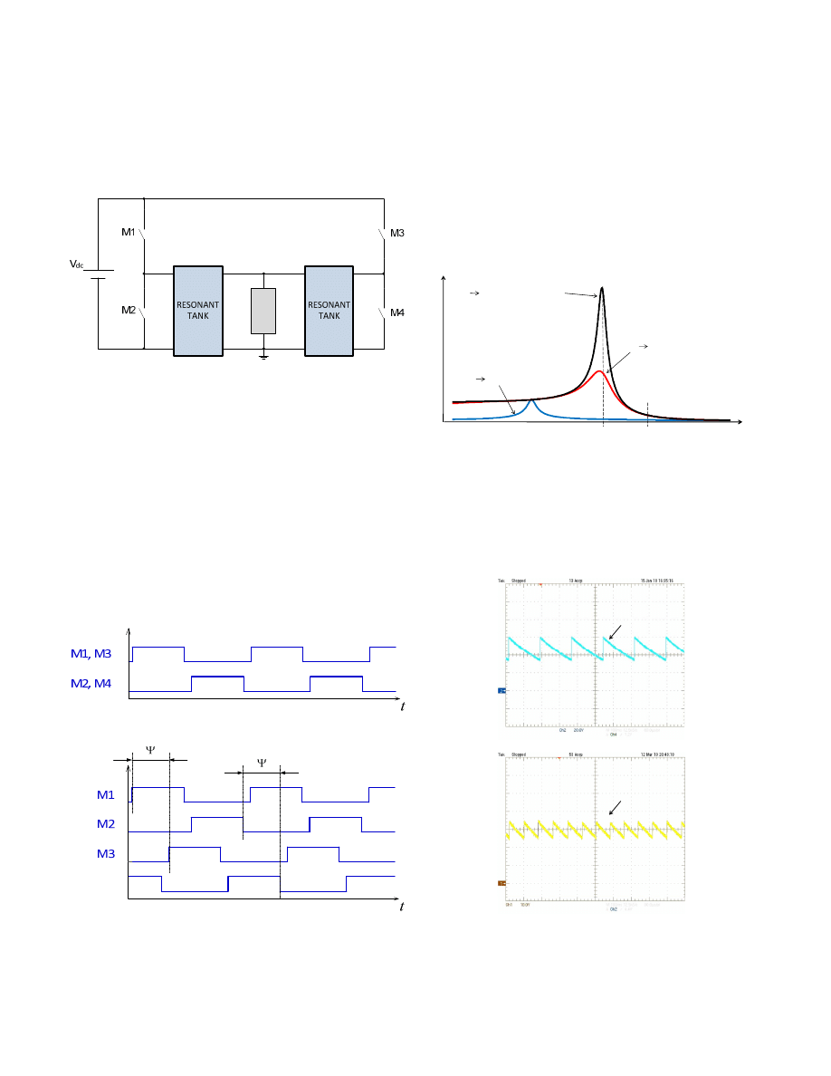
Fig. 2 shows the two-phase resonant inverter obtained
from the parallel connection of two class D LC
s
C
p
resonant
inverters [2], [3].
LO
A
D
Fig. 2. Block diagram of the resonant inverter.
In welding operation, the circuit operates as a current
source switching at 125 kHz, which is the unloaded resonant
frequency. The maximum current is obtained when M1 and
M3 switch synchronously and alternately to M2 and M4, as
shown in Fig. 3. The output current level can be reduced
introducing a phase-shift (
Ψ) between the drive signals of
each inverter, as shown in Fig. 4.
The output voltage is imposed by the welding process
from 6 V to 15 V, in the case of TIG welding, up to 35 V, for
SMAW. In stand-by conditions, the circuit has to be
protected against over voltage. This voltage charges the
output capacitor that provides the electric discharge necessary
to establish the arc.
Fig. 3. On phase.
Fig. 4. Sliding phase.
For turning the power supply off, the switching frequency
is fixed at 250 kHz, at this frequency the voltage gain of the
resonant inverter is very low so the output voltage decreases
drastically as shown in Fig. 5.
In stand-by, due to the resonant circuit operation, the
output voltage rises quickly [4] when switching at 125 kHz,
until reaching a threshold. This limit, set at 40 V to protect
the power supply, is implemented by means of an opto-
coupler. After this highest threshold has been reached, the
resonant stage switches at 250 kHz and so the voltage falls to
the lowest threshold (hysteresis inherent for this device)
where the resonant stage will switch at 125 kHz again, and so
on until the weld operation starts.
V
ol
tag
e
gai
n
f (kHz)
125 kHz
250 kHz
Q
p
arc
Q
p
dielectric breakdown
Q
p
short circuit
Fig. 5. Resonant inverter voltage gain vs. frequency.
In Fig. 6(a), the output voltage of the arc welding power
supply, v
o
, is shown in open circuit conditions.
A new method is proposed to minimize the output voltage
ripple, amplitude and frequency under open circuit
conditions. The practical advantage of the method is the
significant size reduction of the output capacitor.
20 V/div, 100 ms/div
v
o
(a)
10 V/div, 100 ms/div
v
o
(b)
Fig. 6. Output voltage in stand-by operation: a) open circuit in current
system and b) soft start.
An improved operation mode is achieved when a sliding
phase is introduced (soft-start), decreasing the output current
level as well as the resonant inverter voltage gain. Fig. 6(b)
shows the output voltage, v
o
, in this operation mode. As
observed, the output ripple and amplitude are reduced and the
frequency is increased which allows the size to be reduced
and extends the life of the output capacitor.
3.2. Resonant inductance specifications
The resonant inverter stage is composed of modules which
supply up to 25 A. Every module has been designed to work
at 1 kW as maximum power. In nominal behavior, the drop
voltage in the resonant inductor is about 1 kV but in stand-by
operation, this voltage increases up to 1.3 kV as shown in
Fig. 7(a). For this reason, the specification in resonant
inductance should be higher, increasing its size and weight.
By means of the sliding phase described in Section 3.1,
lower energy circulates in the resonant tank reducing the
maximum resonant inductor voltage (around 800 V), as
shown in the lower trace of Fig. 7(b), which means that the
voltage specification does not exceed the voltage required for
the nominal operation.
500 V/div, 10 µs/div
v
L
(a)
1 kV/div, 20 µs/div
v
L
(b)
Fig. 7. Resonant inductor voltage in stand-by operation: a) open circuit
without sliding phase and b) open circuit with sliding phase.
3.3. Interleaving effects in output capacitor current
The transformer supplies a high-frequency current. After
rectification, the ac component is removed by the inductance
of the wires that connect the converter output to the torch.
(a) (b)
Fig. 8. Output current: a) on-phase and b) interleaving operation.
Further reduction of the capacitor current ripple is
achieved by the interleaving operation of paralleled stages
[5], [6]. In this mode, the MOSFETs’ drive signals of one
stage are delayed 90 degrees with respect to the others. The
theoretical output current waveforms of on-phase and
interleaved operation are depicted in Fig. 8.
Instantaneous output voltage differences between two
paralleled stages, which occur in the interleaving operation,
drop across the connection wires. The wire impedance
prevents cross-current conduction between paralleled stages.
The benefit of the interleaving operation is shown in Fig.
9, in which the output capacitor ripple in the case of on-phase
and interleaving operation are compared. Fig. 9 also includes
the waveforms of one rectifier diode voltage of two paralleled
stages. In Fig. 9(b) a 90-degree phase difference between the
diode voltages can be observed.
(a)
(b)
Fig. 9. Ac current in capacitor (Ch1), output current (Ch2), VD1,1 (Ch3),
VD2,1 (Ch4): a) on-phase and b) interleaving operation. Ch1: 25 A/div; Ch2:
20 A/div; Ch3, Ch4: 20 V/div; time scale: 4 µs/div.
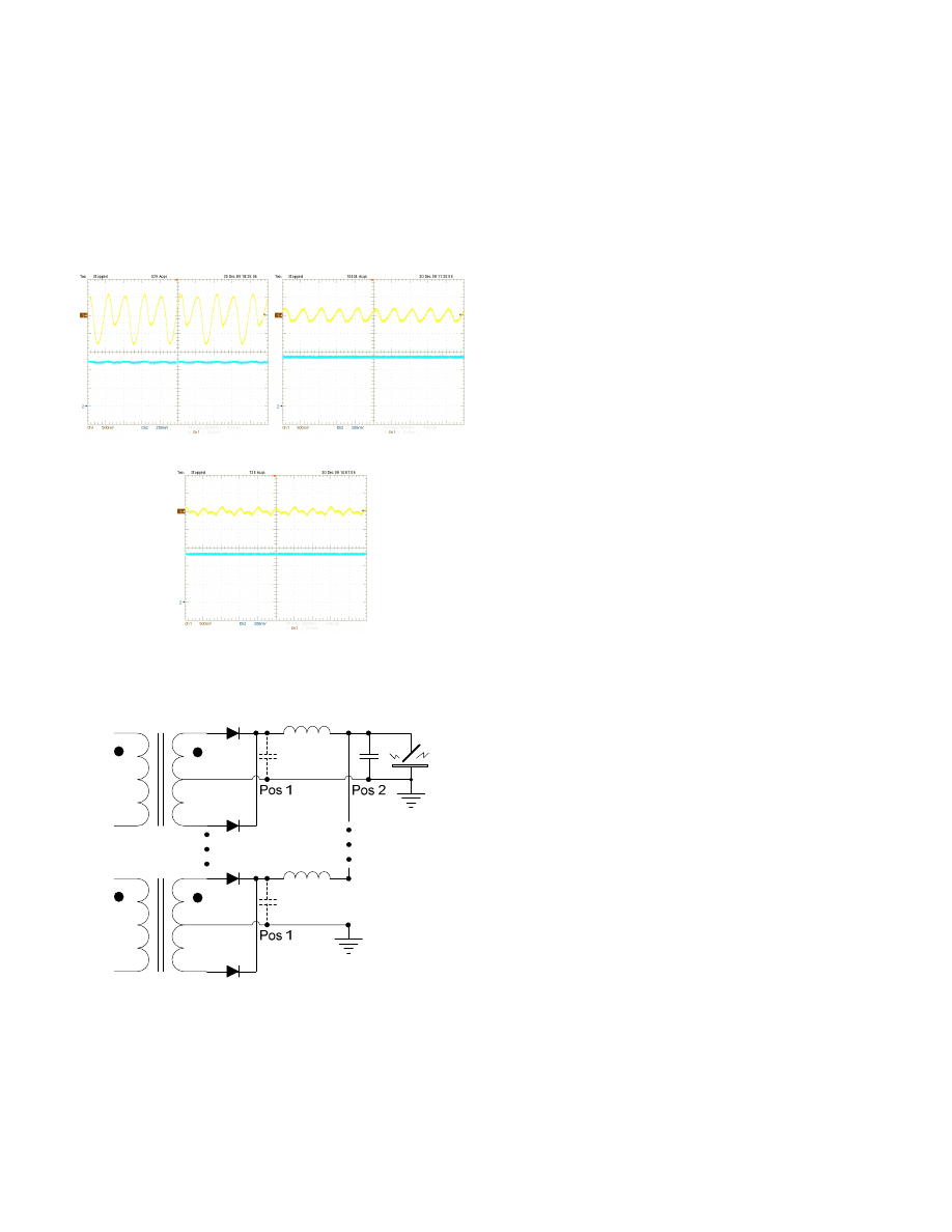
Fig. 10 shows the effect of the wire impedance and the
interleaving operation in the output capacitor current. Fig.
10(a) shows the capacitor current and the output current with
the capacitor in position Pos 1 (see Fig. 11). Fig. 10(b) shows
the same waveforms with the capacitor in position Pos 2 (see
Fig. 11). Fig. 10(c) shows the same waveforms with the
capacitor in position Pos 2 (see Fig. 11) and interleaving
operation.
(a) (b)
(c)
Fig. 10. Ac current in capacitor (Ch1) and output current (Ch2): a) capacitor
in Pos 1, b) capacitor in Pos 2 and c) capacitor un Pos 2 and interleaving
operation. Ch1: 25 A/div; Ch2: 20 A/div; time scale: 4 µs/div.
Fig. 11. HF rectification.
3.4. Synchronous rectification
Traditionally, the rectifier devices are diodes, but due to
the evolution of the MOSFETs [7], in some applications it is
possible to use them to reduce conduction losses:
2
,
,
rms
o
d
dc
o
f
diode
I
r
I
V
P
+
=
(1)
2
,
)
(
rms
o
on
ds
MOSFET
I
R
P
=
(2)
Synchronous rectification (SR) is used in applications in
which low voltage, high current and fast dynamic response
are required. Improved performance and thermal behavior
and reduced size are achieved by using this technique.
Depending on how the MOSFETs’ drive signals are
generated, two types of SR are distinguished: 1) self driven
and 2) external driven:
1) Self driven:
The main advantage is its simplicity because no further
signals are required [8]-[10]. This type of SR is used in
topologies where fast switching transition leads to short dead-
time, reducing the power losses that the current circulating
across the MOSFETs’ body diodes would produce otherwise.
As a limitation, the correct MOSFET excitation depends
on the drain to source voltage; to establish a dead time
between two synchronous rectifiers, a low voltage does not
turn the switches on. If the resulting dead time is long, it may
lead to high switching losses.
2) External driven:
In this type of rectification the MOSFETs’ drive signals
are generated by an external control circuit [11], [12].
– The main advantages are:
Since the MOSFETs’ drive signals depend of the control
circuit, the dead time can be managed efficiently,
decreasing power losses on the parasitic diode.
• The gate to source voltage is independent of the drain
to source voltage.
– On the other hand, the drawbacks are:
• There is no automatic synchronism between power
and control stages, so the external circuit is
responsible for driving the devices.
• The drive signal may require galvanic isolation. In
this case a pulse transformer or opto-coupler with the
appropriate bandwidth should be selected.
• External power supplies are required.
For this application, the external driven mode, by means of
an IC driver, is selected [13], [14]. As mentioned in [13], the
rectifier currents in the two secondary legs are sensed using
the power MOSFET R
ds(on)
as a shunt resistance. The
MOSFET drive signals are generated by comparing the
sensed voltage to three thresholds.
The core of this device is the two high-speed comparators
which differentially sense the drain-to-source voltage of the
switch, in order to determine the polarity and level of the
switch currents. Then, a dedicated internal logic manages the
MOSFET switching in close proximity to the zero current
transition, assuring accurate performance without needing a
PLL or an external timing source. Additionally, an internal
blanking logic is used to prevent spurious gate transitions and
to guarantee operation in fixed and variable frequency
operation modes.
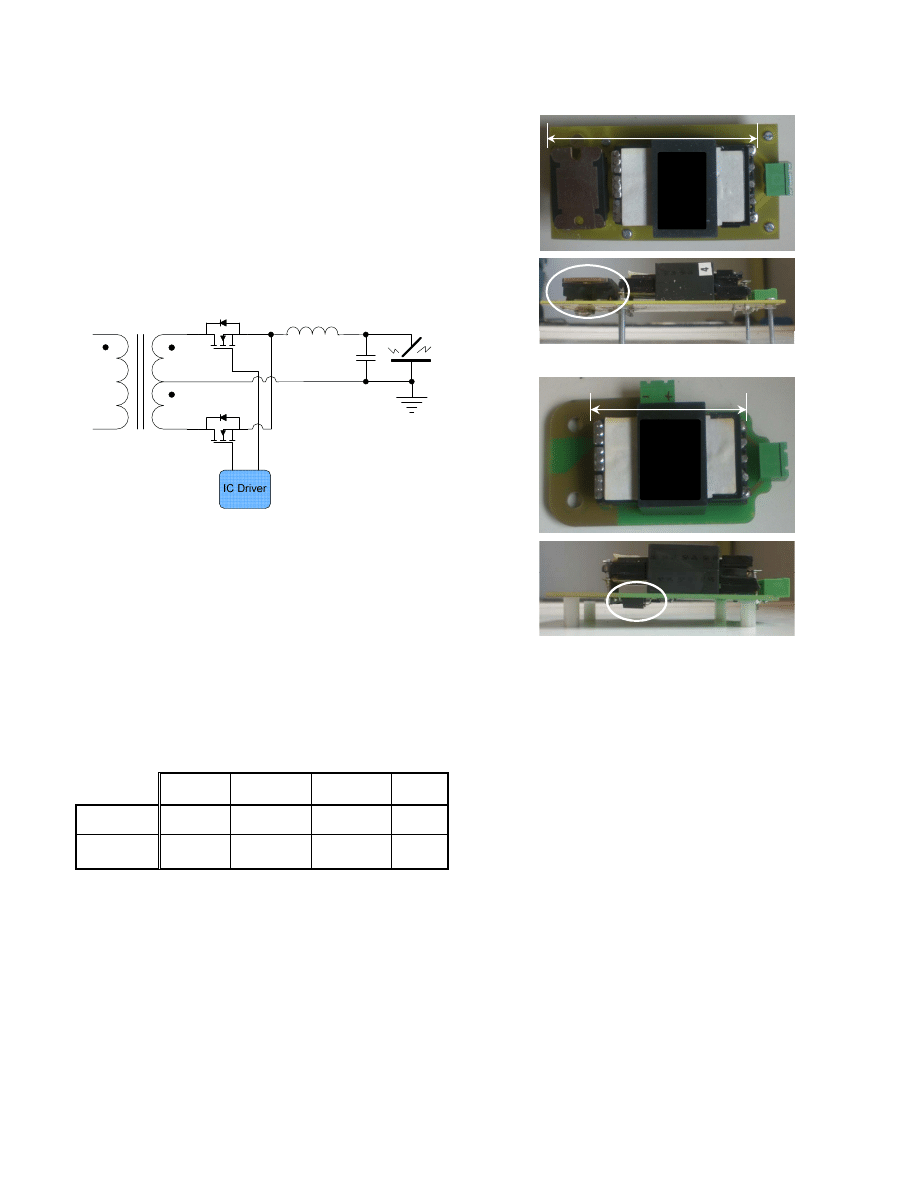
By implementing this rectification technique (see Fig. 12),
the dissipated power is reduced and consequently the rectifier
device temperature, leading to better performance. Thus, the
size of the heatsink can also be reduced and the total size will
be less for this stage and so to the overall system.
The prototype built for this application is composed of
twelve 25 A modules, making up a total system that can
supply up to 300 A.
Fig. 12. Synchronous rectification based on IC driver.
Different tests have been performed to compare the
efficiency using diodes vs. power MOSFETs as a SR. The
power Schottky diodes are IXYS Semiconductor DSS
2X101-015A (V
RRM
= 150 V, I
FAV
= 2x100 A, V
F
= 0.77 V)
and the power MOSFETs are IRLS4030 (V
DSS
= 100 V, I
D
=
190 A, R
DS(on)max.
= 3.9 mΩ). These tests are carried out using
a 2 Ω resistor. The results are shown in Table I.
The input power is measured at the input of the inverter
stage and the output voltage is measured at the load
calculating the output power.
TABLE
I
C
OMPARISON
:
D
IODES VS
.
MOSFET
S
P
in,ms
(W) V
out,rms
(V) P
out,rms
(W) η (%)
Diodes 930 39.8 792.02
85.16
MOSFETs 952
40.6 824.18 86.57
As shown in Table I, the results obtained using power
MOSFETs are better than using diodes. Using synchronous
rectification, the power loss has been improved 1.41 W in
each rectifier stage.
Fig. 13 and Fig. 14 show photographs of different layouts
of the output stage without heatsinks and the size reduction of
the rectification stage can be observed.
95 mm
Fig. 13. Rectification stage using diodes.
67 mm
Fig. 14. Rectification stage using external driven MOSFETs.
3.5. Establishing and extinguishing arc sequence
Different analyses of arc discharge have been carried out
over time [15], [16] to determine criteria for arc ignition.
Three methods can be used to start the arc:
1. contact [17], [18],
2. applying a high-voltage pulse or
3. high-voltage high-frequency ac pulses (HV-HF) [19],
[20].
Method 1 is selected since no extra circuitry is required
and it is compatible with the proposed rectifier stages (either
Schottky diodes or synchronous rectification). Furthermore, a
modification of this technique is presented to establish the
welding arc minimizing damage to the metal parts and
reducing electromagnetic interferences (EMI) produced in
electronic devices located near the circuit compared to the
HV-HF method.
When the arc starts or ends, two types of damage can be
produced:
a) electrode and workpiece deterioration and possible
contamination can occur due to the welding sparks, and
b) a crater can be formed which will be the origin of
cracks in the welded part.
To minimize or even eliminate these negative effects, the
proposed system can establish the arc welding touching the
electrodes together at a low current level and then increasing
up to the required current by means of the sliding phase, as
explained in Section 3.1 (Fig. 4), in a period denominated up-
slope. Due to the use of a control circuit based on a field
programmable gate array (FPGA) device, the period of the
up-slope can be easily changed according to the operation
needs.
Similarly a down-slope period is defined to extinguish the
arc. A sliding phase is performed in order to slowly reduce
the output current level.
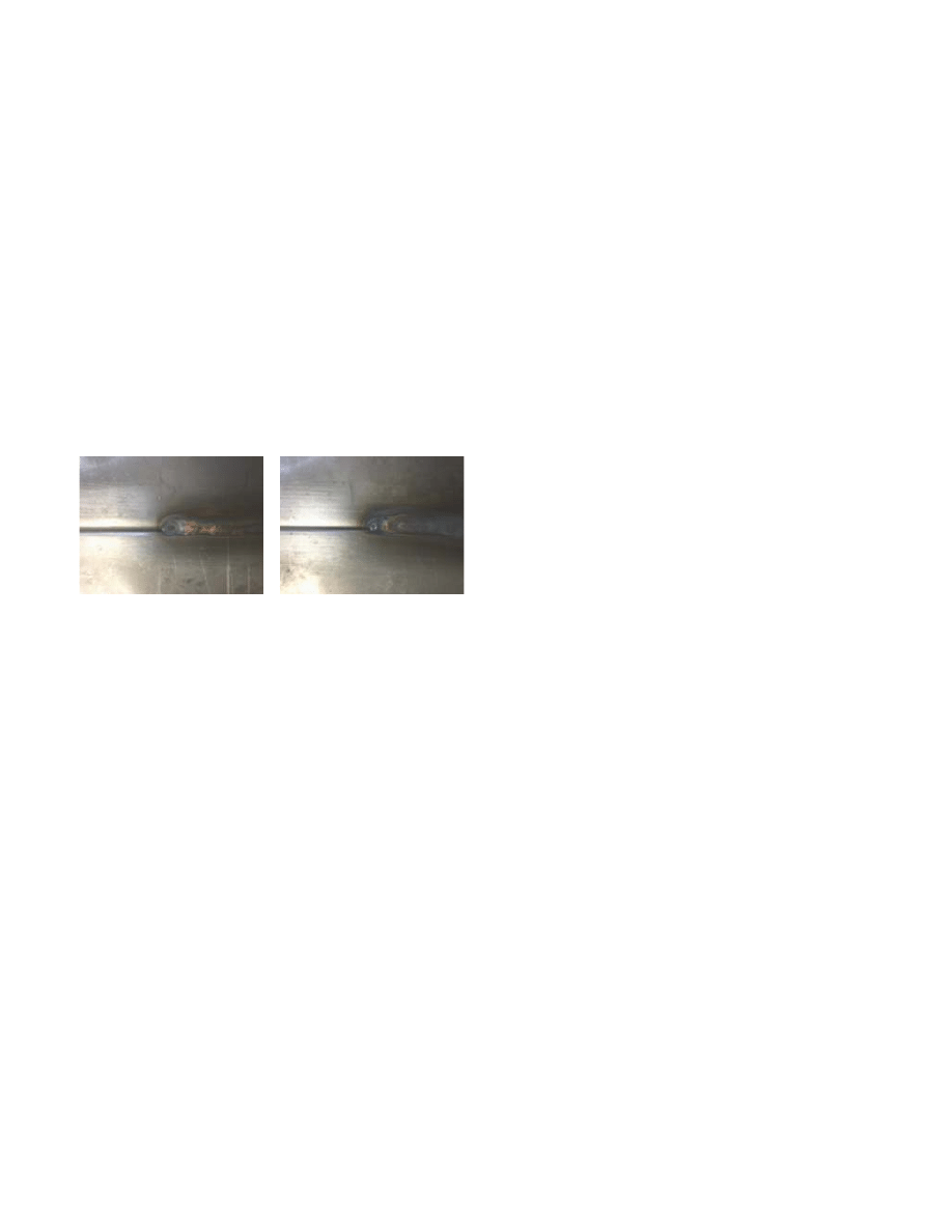
Fig. 15 shows photographs of two weld beads with
different extinguishing arc sequences. The tests have been
carried out on 3 mm thick AISI 316 steel plates, for a current
setup of the power supply of 100 A. In Fig. 15(a), the arc is
abruptly finished and in Fig. 15(b) the output current was
reduced with a down-slope of ~14 A/s. Differences are found
in the resulting crater size.
Crater Ø=6 mm
Crater Ø=2.5 mm
(a) (b)
Fig. 15. Extinguishing arc: (a) abrupt and (b) by means of a down-slope.
IV. C
ONCLUSIONS
In this paper, improvements for an arc-welding power
supply based on resonant inverters have been developed. The
output voltage ripple, amplitude and frequency under open
circuit conditions have been reduced by means of a sliding
phase, which increases the life time of the output capacitor. In
the same way, the resonant inductance voltage in stand-by
operation has been reduced in order to reduce its size and
weight. The effects of the ac output current have been shown
and have been improved by means of interleaving the current
ripple of different stages. The diodes of the rectifier stage
have been replaced by power MOSFETs in order to increase
performance and reduce temperature in these rectifier devices
and to achieve a smaller layout of this stage. Finally, an
improved method for starting and extinguishing the arc has
been developed to reduce damage in the welded parts.
A
CKNOWLEDGMENT
This work is sponsored by the Spanish Government in the
framework of the project CICYT TEC2008-01753 entitled:
“Digital power processing for the control of gaseous
discharges”.
R
EFERENCES
[1] R. Casanueva, F. J. Azcondo, F. J. Diaz and C. Branas, "DC and Pulsed
DC TIG Welding with a Scalable Power Supply," in Proc. IEEE IAS
2009, pp. 1-6.
[2] D. Czarkowski, M. K. Kazimierczuk, "Phase-Controlled Series-Parallel
Resonant Converter," IEEE Trans. on Power Electron. , vol. 8, no. 3,
pp. 309-319, July 1993.
[3] C. Brañas, F. J. Azcondo, R. Casanueva, S. Bracho, “Multi-Phase
Parallel Resonant Inverter Applied to HID Lamp Control,” in Proc.
PCIM Europe 2005, pp. 187-192.
[4] L. Malesani, P. Mattavelli, L. Rossetto, P. Tenti, W. Marin, A.
Pollmann, “Electronic welder with high-frequency resonant inverter,”
IEEE Trans. on Industry Applications, vol. 31. Issue 2, pp. 273–279,
March/April 1995.
[5] R. Casanueva, F. J. Azcondo, C. Branas and S. Bracho , "High spark,
low loss - paralleled LC
S
C
p
resonant converters for spark erosion
applications," IEEE Industry Applications Magazine, vol. 12, no. 2, pp.
43- 51, March-April 2006.
[6] J. B. Klaassens, W. L. F. H. A. Moize de Chateleux, M. P. N. Van
Wesenbeeck, “Phase-Staggering Control of a Series-Resonant DC-DC
Converter with Paralleled Power Modules,” IEEE Trans. on Power
Electron., vol. 3, no. 2, pp. 164-173, April 1988.
[7] C. Blake, D. Kinzer and P. Wood, "Synchronous rectifiers versus
Schottky diodes: a comparison of the losses of a synchronous rectifier
versus the losses of a Schottky diode rectifier," in Proc. IEEE APEC
1994, vol. 1, pp. 17-23.
[8] J. A. Cobos, O. Garcia, J. Sebastian and J. Uceda, "Active clamp PWM
forward converter with self-driven synchronous rectification," in Proc.
IEEE INTELEC 1993, vol. 2, pp. 200-206.
[9] O. Garcia, J. A. Cobos, J. Uceda and J. Sebastian, "Zero voltage
switching in the PWM half bridge topology with complementary
control and synchronous rectification," in Proc. IEEE PESC 1995, vol.
1, pp. 286-291.
[10] J. A. Cobos, J. Sebastian, J. Uceda, E. de la Cruz and J. M. Gras,
"Study of the applicability of self-driven synchronous rectification to
resonant topologies," in Proc. IEEE PESC 1992, vol. 2, pp. 933-940.
[11] D. Huang, D. Fu and F. C. Lee, "High switching frequency, high
efficiency CLL resonant converter with synchronous rectifier," in Proc.
IEEE ECCE 2009, pp. 804-809.
[12] C. Yan, F. Li, J. Zeng and J. Ying, "A High Efficiency 3 KW DC/DC
Converter with Novel External Driven Synchronous Rectifier," in Proc.
IEEE INTELEC 2004, pp. 638-641.
[13] International Rectifier, “Dual Smart rectifier driver IC,” IR1168S
datasheet, Nov. 2009.
[14] A. Lokhandwala, “Design of Secondary-Side Rectification using
IR1168 Dual SmartRectifier™ Control IC,” International Rectifier,
Application Note AN-1139.
[15] J. Leland Myer, "New Studies of the Arc Discharge," Transactions of
the American Institute of Electrical Engineers, vol. 52, no. 1, pp. 250-
259, March 1933.
[16] L. L. Alston, "The impulse initiation of arc discharges," Proceedings of
the IEE-Part A: Power Engineering, vol. 106, no. 26, pp. 133-140,
April 1959.
[17] H. Edels, “A technique for arc initiation,” British Journal of Applied
Physics, vol. 2, pp. 171-174, 1951.
[18] J. B. Bjorgvinsson, R. J. Barnett, G. E. Cook and K. Andersen,
"Microprocessor control of arc starting for gas tungsten arc welding
(GTAW)," in Proc. IEEE SoutheastCon 1990, vol. 3, pp. 787-791.
[19] A. K. Paul, “Optimizing the Transition Process from Sparking for Non-
contact TIG Welding Inverters,” in Proc. IEEE ICIT 2006, pp. 1413-
418.
[20] J. A. Ferreira, J. A. Roux, “A Series Resonant Converter for Arc-
Striking Applications,” IEEE Trans. Ind. Electron., vol. 45, no. 4, pp.
585-592, Aug. 1998.
Wyszukiwarka
Podobne podstrony:
Paralleling Arc Welding Power Sources
How to Modify an ATX Computer Power Supply
Paralleling Arc Welding Power Sources
A Series Active Power Filter Based on a Sinusoidal Current Controlled Voltage Source Inverter
A Series Active Power Filter Based on Sinusoidal Current Controlled Voltage Source Inverter
A Series Active Power Filter Based on Sinusoidal Current Controlled Voltage Source Inverter
Improvements in Fan Performance Rating Methods for Air and Sound
Iannace, Ianniello, Romano Room Acoustic Conditions Of Performers In An Old Opera House
Control and Power Supply for Resistance Spot Welding (RSW)
Power MOS FET in Switching Power Supply
Improvements in Fan Performance Rating Methods for Air and Sound
Canadian Patent 29,537 Improvements in Methods of and Apparatus for the Electrical Transmission of P
Convert Computer ATX Power Supply to Lab Power Supply
Jvc Power Supply Description And Trouble Shooting Procedure
Battery Inverter For Modularly Structured Pv Power Supply Systems
0 50V 2A LM10C, 0 50V 2A Bench power supply circuit diagrams, schematics, electronic projects
więcej podobnych podstron