1
LTC1090
1090fc
Single Chip 10-Bit Data
Acquisition System
■
Software Programmable Features:
Unipolar/Bipolar Conversions
4 Differential/8 Single Ended Inputs
MSB or LSB First Data Sequence
Variable Data Word Length
■
Built-In Sample and Hold
■
Single Supply 5V, 10V or ±5V Operation
■
Direct 4 Wire Interface to Most MPU Serial Ports and
All MPU Parallel Ports
■
30kHz Maximum Throughput Rate
■
Resolution: 10 Bits
■
Total Unadjusted Error (LTC1090A): ±1/2LSB Max
■
Conversion Time: 22µs
■
Supply Current: 2.5mA Max, 1.0mA Typ
The LTC
®
1090 is a data acquisition component which
contains a serial I/O successive approximation A/D con-
verter. It uses LTCMOS
TM
switched capacitor technology
to perform either 10-bit unipolar, or 9-bit plus sign bipolar
A/D conversions. The 8-channel input multiplexer can be
configured for either single ended or differential inputs (or
combinations thereof). An on-chip sample and hold is
included for all single ended input channels.
The serial I/O is designed to be compatible with industry
standard full duplex serial interfaces. It allows either
MSB or LSB first data and automatically provides 2’s
complement output coding in the bipolar mode. The
output data word can be programmed for a length of 8, 10,
12 or 16 bits. This allows easy interface to shift registers
and a variety of processors.
The LTC1090A is specified with total unadjusted error
(including the effects of offset, linearity and gain errors)
less than ±0.5LSB.
The LTC1090 is specified with offset and linearity less than
±0.5LSB but with a gain error limit of ±2LSB for
applications where gain is adjustable or less critical.
FEATURES
DESCRIPTIO
U
LTCMOS is a trademark of Linear Technology Corp.
, LTC and LT are registered trademarks of Linear Technology Corporation.
KEY SPECIFICATIO S
U
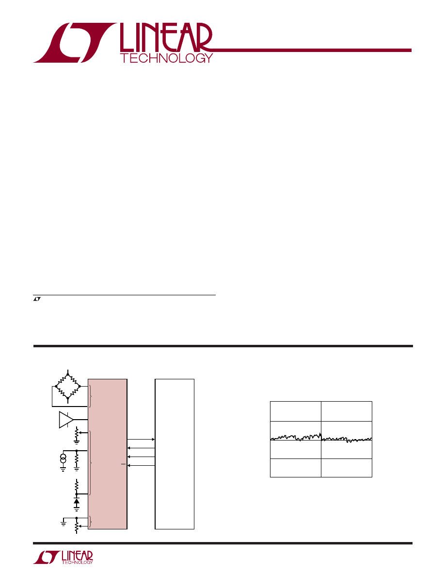
LTC1090 • TA02
OUTPUT CODE
0
512
1024
ERROR (LSBs)
1.0
0.5
0.0
– 0.5
–1.0
Linearity Plot
TYPICAL APPLICATIO
U
5V
LTC1090
MPU
(e.g., 8051)
FOR 8051 CODE SEE
APPLICATIONS INFORMATION
SECTION
DIFFERENTIAL
INPUT
BIPOLAR INPUT
–5V
5V
–5V
(+)
(–)
T
LTC1090 • TA01
UNIPOLAR
INPUTS
P1.1
D
OUT
P1.2
D
IN
P1.3
SCLK
P1.4
CS
SERIAL DATA
LINK
– UNIPOLAR
INPUT
2
LTC1090
1090fc
ABSOLUTE AXI U RATI GS
W
W
W
U
Supply Voltage (V
CC
) to GND or V
– ................................
12V
Negative Supply Voltage (V
–
) ..................... – 6V to GND
Voltage:
Analog and Reference
Inputs .................................... (V
–
) –0.3V to V
CC
0.3V
Digital Inputs ......................................... –0.3V to 12V
Digital Outputs .............................. – 0.3V to V
CC
0.3V
Power Dissipation .............................................. 500mW
Operating Temperature Range
LTC1090AC/LTC1090C ........................–40°C to 85°C
LTC1090AM/LTC1090M (OBSOLETE) ...... –55°C to 125°C
Storage Temperature Range ................. – 65°C to 150°C
Lead Temperature (Soldering, 10 sec).................. 300°C
(Notes 1 and 2)
PACKAGE/ORDER I FOR ATIO
U
U
W
Consult LTC Marketing for parts specified with wider operating temperature
ranges.
RECO
E
DED OPERATI
G CO DITIO
S
U
U
U
U
W
W
LTC1090/LTC1090A
SYMBOL
PARAMETER
CONDITIONS
MIN
MAX
UNITS
V
CC
Positive Supply Voltage
V
–
= 0V
4.5
10
V
V
–
Negative Supply Voltage
V
CC
= 5V
– 5.5
0
V
f
SCLK
Shift Clock Frequency
V
CC
= 5V
0
1.0
MHz
f
ACLK
A/D Clock Frequency
V
CC
= 5V
25°C
0.01
2.0
MHz
85°C
0.05
2.0
125°C
0.25
2.0
t
CYC
Total Cycle Time
See Operating Sequence
10 SCLK +
Cycles
48 ACLK
t
hCS
Hold Time, CS Low After Last SCLK↓
V
CC
= 5V
0
ns
t
hDI
Hold Time, D
IN
After SCLK
↑
V
CC
= 5V
150
ns
t
suCS
Setup Time CS
↓ Before Clocking in First Address Bit (Note 9)
V
CC
= 5V
2 ACLK Cycles
1µs
t
suDI
Setup Time, D
IN
Stable Before SCLK↑
V
CC
= 5V
400
ns
t
WHACLK
ACLK High Time
V
CC
= 5V
127
ns
t
WLACLK
ACLK Low Time
V
CC
= 5V
200
ns
t
WHCS
CS High Time During Conversion
V
CC
= 5V
44
ACLK
Cycles
OBSOLETE PACKAGE
Consider the SW or N Package for Alternate Source
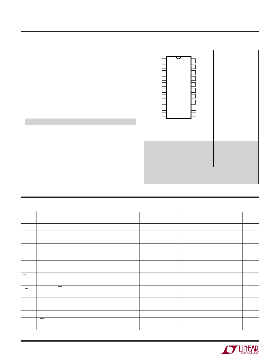
1
2
3
4
5
6
7
8
9
10
TOP VIEW
J PACKAGE
20-LEAD CERDIP
T
JMAX
= 150
°
C
θ
JA
= 70
°
C/W
SW PACKAGE
20-LEAD PLASTIC SO WIDE
N PACKAGE
20-LEAD PDIP
20
19
18
17
16
15
14
13
12
11
CH0
CH1
CH2
CH3
CH4
CH5
CH6
CH7
COM
DGND
V
CC
ACLK
SCLK
D
IN
D
OUT
CS
REF
+
REF
–
V
–
AGND
LTC1090ACN
LTC1090CN
LTC1090CSW
LTC1090AMJ
LTC1090MJ
LTC1090ACJ
LTC1090CJ
ORDER PART
NUMBER
T
JMAX
= 150
°
C,
θ
JA
= 70
°
C/W
T
JMAX
= 110
°
C,
θ
JA
= 90
°
C/W
LTC1090 • POI01
3
LTC1090
1090fc
CO VERTER A D ULTIPLEXER CHARACTERISTICS
U
W
U
LTC1090A
LTC1090
PARAMETER
CONDITIONS
MIN
TYP
MAX
MIN
TYP
MAX
UNITS
Offset Error
(Note 4)
●
±0.5
±0.5
LSB
Linearity Error
(Notes 4 and 5)
●
±0.5
±0.5
LSB
Gain Error
(Note 4)
●
±1.0
±2.0
LSB
Total Unadjusted Error
V
REF
= 5.000V
●
±1.0
LSB
(Notes 4 and 6)
Reference Input Resistance
10
10
kΩ
Analog and REF Input Range
(Note 7)
(V
–
) – 0.05V to V
CC
0.05V
V
On Channel Leakage Current
On Channel = 5V
●
1
1
µA
(Note 8)
Off Channel = 0V
On Channel = 0V
●
–1
–1
µA
Off Channel = 5V
Off Channel Leakage Current
On Channel = 5V
●
–1
–1
µA
(Note 8)
Off Channel = 0V
On Channel = 0V
●
1
1
µA
Off Channel = 5V
The
●
denotes specifications which
apply over the full operating temperature range, otherwise specifications are T
A
= 25°C. (Note 3)
LTC1090/LTC1090A
SYMBOL
PARAMETER
CONDITIONS
MIN
TYP
MAX
UNITS
t
ACC
Delay Time From CS↓ to D
OUT
Data Valid
(Note 9)
2
ACLK Cycles
t
SMPL
Analog Input Sample Time
See Operating Sequence
5
SCLK Cycles
t
CONV
Conversion Time
See Operating Sequence
44
ACLK Cycles
t
dDO
Delay Time, SCLK
↓ to D
OUT
Data Valid
See Test Circuits
●
250
450
ns
t
dis
Delay Time, CS
↑ to D
OUT
Hi-Z
See Test Circuits
●
140
300
ns
ns
t
en
Delay Time, 2nd CLK
↓ to D
OUT
Enabled
See Test Circuits
●
150
400
ns
ns
t
hDO
Time Output Data Remains Valid After SCLK
↓
50
ns
t
f
D
OUT
Fall Time
See Test Circuits
●
90
300
ns
ns
t
r
D
OUT
Rise Time
See Test Circuits
●
60
300
ns
ns
C
IN
Input Capacitance
Analog Inputs
On Channel
65
pF
Off Channel
5
pF
Digital Inputs
5
pF
The
●
denotes specifications which apply over the full operating
temperature range, otherwise specification are T
A
= 25°C. (Note 3)
AC ELECTRICAL CHARACTERISTICS
4
LTC1090
1090fc
DIGITAL A D DC ELECTRICAL CHARACTERISTICS
U
LTC1090/LTC1090A
SYMBOL
PARAMETER
CONDITIONS
MIN
TYP
MAX
UNITS
V
IH
High Level lnput Voltage
V
CC
= 5.25V
●
2.0
V
V
IL
Low Level Input Voltage
V
CC
= 4.75V
●
0.8
V
I
IH
High Level lnput Current
V
IN
= V
CC
●
2.5
µA
I
IL
Low Level Input Current
V
IN
= 0V
●
–2.5
µA
V
OH
High Level Output Voltage
V
CC
= 4.75V, l
O
= 10µA
4.7
V
V
CC
= 4.75V, l
O
= 360µA
●
2.4
4.0
V
V
OL
Low Level Output Voltage
V
CC
= 4.75V, l
O
= 1.6mA
●
0.4
V
I
OZ
Hi-Z Output Leakage
V
OUT
= V
CC
, CS High
●
3
µA
V
OUT
= 0V, CS High
●
–3
µA
I
SOURCE
Output Source Current
V
OUT
= 0V
–10
mA
I
SINK
Output Sink Current
V
OUT
= V
CC
10
mA
I
CC
Positive Supply Current
CS High, REF
+
Open
●
1.0
2.5
mA
I
REF
Reference Current
V
REF
= 5V
●
0.5
1.0
mA
I
–
Negative Supply Current
CS High, V
–
= – 5V
●
1
50
µA
The
●
denotes specifications which apply
over the full operating temperature range, otherwise specification are T
A
= 25°C. (Note 3)
Note 1: Absolute Maximum Ratings are those values beyond which the life
of a device may be impaired.
Note 2: All voltage values are with respect to ground with DGND, AGND
and REF
–
wired together (unless otherwise noted).
Note 3: V
CC
= 5V, V
REF
+ = 5V, V
REF
– = 0V, V
–
= 0V for unipolar mode and
–5V for bipolar mode, ACLK = 2.0MHz, SCLK = 0.5MHz unless otherwise
specified.
Note 4: These specs apply for both unipolar and bipolar modes. In bipolar
mode, one LSB is equal to the bipolar input span (2V
REF
) divided by 1024.
For example, when V
REF
= 5V, 1LSB (bipolar) = 2(5V)/1024 = 9.77mV.
Note 5: Linearity error is specified between the actual end points of the
A/D transfer curve.
Note 6: Total unadjusted error includes offset, gain, linearity, multiplexer
and hold step errors.
Note 7: Two on-chip diodes are tied to each reference and analog input
which will conduct for reference or analog input voltages one diode drop
below V
–
or one diode drop above V
CC
. Be careful during testing at low
V
CC
levels (4.5V), as high level reference or analog inputs (5V) can cause
this input diode to conduct, especially at elevated temperatures, and cause
errors for inputs near full-scale. This spec allows 50mV forward bias of
either diode. This means that as long as the reference or analog input does
not exceed the supply voltage by more than 50mV, the output code will be
correct. To achieve an absolute 0V to 5V input voltage range will therefore
require a minimum supply voltage of 4.950V over initial tolerance,
temperature variations and loading.
Note 8: Channel leakage current is measured after the channel selection.
Note 9: To minimize errors caused by noise at the chip select input, the
internal circuitry waits for two ACLK falling edges after a chip select falling
edge is detected before responding to control input signals. Therefore, no
attempt should be made to clock an address in or data out until the
minimum chip select setup time has elapsed.
5
LTC1090
1090fc
On and Off Channel Leakage Current
Voltage Waveforms for D
OUT
Delay Time, t
dDO
Voltage Waveforms for t
en
and t
dis
TEST CIRCUITS
SCLK
0.8V
2.4V
0.4V
2.4V
t
r
t
f
0.4V
t
dDO
D
OUT
D
OUT
LTC1090 • TC02
Voltage Waveforms for D
OUT
Rise and Fall Times, t
r
, t
f
I
ON
5V
OFF
CHANNELS
ON CHANNELS
POLARITY
I
OFF
A
A
LTC1090 • TC01
ACLK
CS
D
OUT
WAVEFORM 1
(SEE NOTE 1)
D
OUT
WAVEFORM 2
(SEE NOTE 2)
1
NOTE 1: WAVEFORM 1 IS FOR AN OUTPUT WITH INTERNAL CONDITIONS SUCH THAT THE OUTPUT
IS HIGH UNLESS DISABLED BY THE OUTPUT CONTROL
NOTE 2: WAVEFORM 2 IS FOR AN OUTPUT WITH INTERNAL CONDITIONS SUCH THAT THE OUTPUT
IS LOW UNLESS DISABLED BY THE OUTPUT CONTROL
2
LTC1090 • TC03
2.4V
90%
2.0V
0.4V
10%
t
en
t
dis
Load Circuit for t
dis
and t
en
Load Circuit for t
dDO
, t
r
, and t
f
3k
100pF
D
OUT
1.4V
TEST POINT
LTC1090 • TC05
WAVEFORM 1
3k
100pF
D
OUT
TEST
POINT
WAVEFORM 2
5V
LTC1090 • TC04
6
LTC1090
1090fc
U
U
U
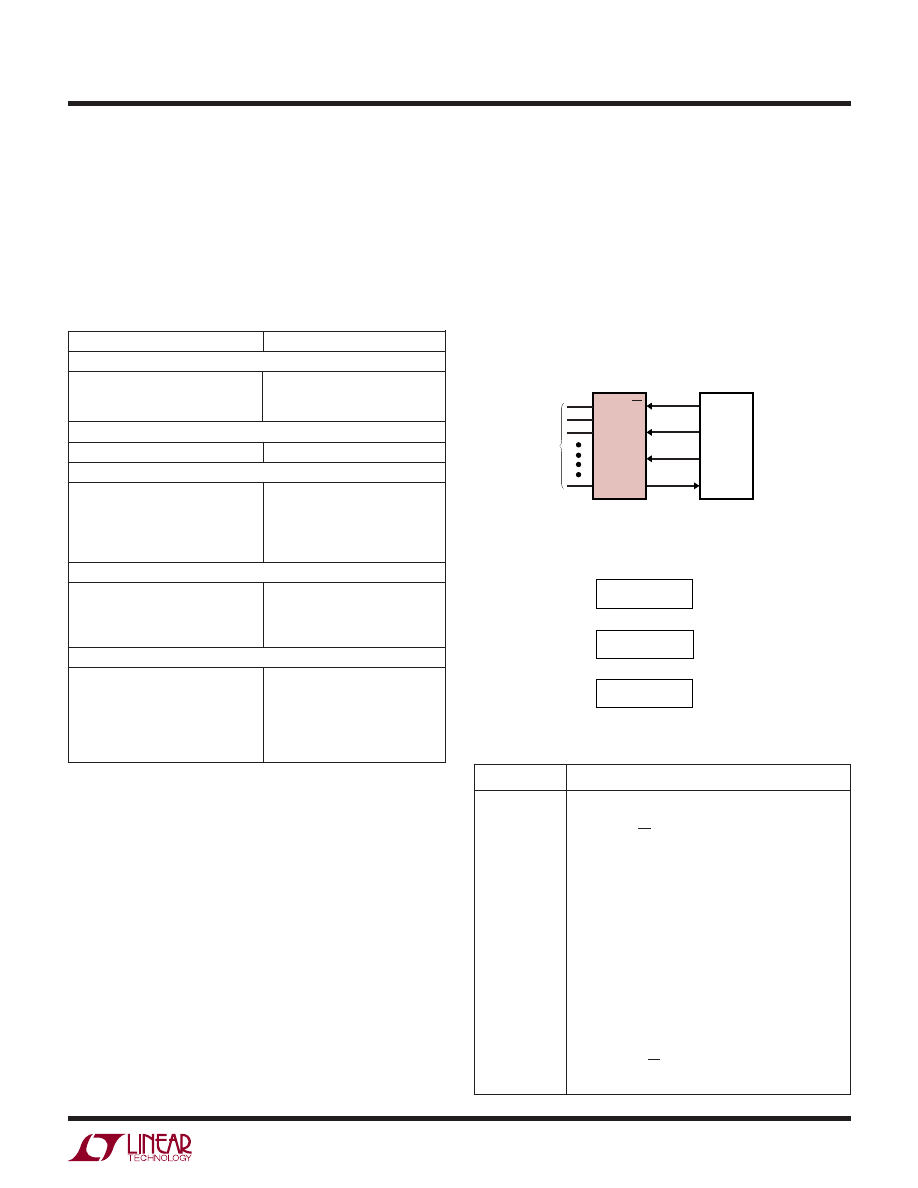
PI FU CTIO S
#
PIN
FUNCTION
DESCRIPTION
1-8
CH0 to CH7
Analog Inputs
The analog inputs must be free of noise with respect to AGND.
9
COM
Common
The common pin defines the zero reference point for all single ended inputs. It must be free
of noise and is usually tied to the analog ground plane.
10
DGND
Digital Ground
This is the ground for the internal logic. Tie to the ground plane.
11
AGND
Analog Ground
AGND should be tied directly to the analog ground plane.
12
V
–
Negative Supply
Tie V
–
to most negative potential in the circuit. (Ground in single supply applications.)
13,14
REF
–
, REF
+
Reference Inputs
The reference inputs must be kept free of noise with respect to AGND.
15
CS
Chip Select Input
A logic low on this input enables data transfer.
16
D
OUT
Digital Data Output
The A/D conversion result is shifted out of this output.
17
D
IN
Data Input
The A/D configuration word is shifted into this input.
18
SCLK
Shift Clock
This clock synchronizes the serial data transfer.
19
ACLK
A/D Conversion Clock
This clock controls the A/D conversion process.
20
V
CC
Positive Supply
This supply must be kept free of noise and ripple by bypassing directly to the analog ground
plane.
BLOCK DIAGRA
W
D
IN
17
D
OUT
16
SCLK
18
LTC1090 • BD01
CH0
1
CH1
2
CH2
3
CH3
4
CH4
5
CH5
6
CH6
7
CH7
8
COM
9
V
CC
20
INPUT SHIFT
REGISTER
OUTPUT
SHIFT
REGISTER
CS
15
ACLK
19
CONTROL
AND
TIMING
10-BIT
SAR
SAMPLE
AND HOLD
ANALOG
INPUT
MUX
COMP
REF –
13
10-BIT
CAPACITIVE
DAC
REF+
V–
12
AGND
11
DGND
10
14
7
LTC1090
1090fc
TYPICAL PERFOR A CE CHARACTERISTICS
U
W
Supply Current vs Supply Voltage
Supply Current vs Temperature
Reference Current vs Temperature
Unadjusted Offset Error vs
Reference Voltage
Linearity Error vs Reference
Voltage
Change in Gain Error vs
Reference Voltage
Offset Error vs Supply Voltage
Linearity Error vs Supply Voltage
Change in Gain Error vs Supply
Voltage
SUPPLY VOLTAGE, V
CC
(V)
4
0
OFFSET ERROR (LSBs)
0.25
0.5
0.75
1.0
1.25
5
6
7
8
LTC1090 • TPC07
9
10
V
REF
= 4V
ACLK = 2MHz
V
OS
= 1.25mV AT V
CC
= 5V
SUPPLY VOLTAGE, V
CC
(V)
4
0
LINEARITY ERROR (LSBs)
0.25
0.5
0.75
1.0
1.25
5
6
7
8
LTC1090 • TPC08
9
10
V
REF
= 4V
ACLK = 2MHz
SUPPLY VOLTAGE, V
CC
(V)
4
CHANGE IN GAIN ERROR (LSBs)
– 0.5
– 0.25
0
0.25
0.5
5
6
7
8
LTC1090 • TPC09
9
10
V
REF
= 4V
ACLK = 2MHz
SUPPLY VOLTAGE, V
CC
(V)
4
0
SUPPLY CURRENT, I
CC
(mA)
1
2
3
4
6
5
6
7
8
LTC1090 • TPC01
9
10
5
REF
+
OPEN
ACLK = 2MHz
CS = V
CC
T
A
= 25°C
AMBIENT TEMPERATURE, T
A
(°C)
–50
SUPPLY CURRENT, I
CC
(mA)
1.0
1.2
1.4
25
75
LTC1090 • TPC02
0.8
0.6
–25
0
50
100
125
0.4
0.2
REF
+
OPEN
ACLK = 2MHz
CS = 5V
V
CC
= 5V
AMBIENT TEMPERATURE, T
A
(°C)
–50
REFERENCE CURRENT, I
REF
(mA)
0.4
0.5
0.6
25
75
LTC1090 • TPC03
0.3
0.2
–25
0
50
100
125
0.1
0
V
REF
= 5V
REFERENCE VOLTAGE, V
REF
(V)
0.2
0
OFFSET ERROR (LSBs = • V
REF
)
2
4
6
8
1.0
5.0
LTC1090 • TPC04
10
1
3
5
7
9
1
1024
V
OS
= 0.5mV
V
OS
= 1mV
V
CC
= 5V
1
1024
REFERENCE VOLTAGE, V
REF
(V)
0
LINEARITY ERROR (LSBs = • V
REF
)
0.75
1.0
1.25
4
LTC1090 • TPC05
0.5
0.25
0
1
2
3
5
V
CC
= 5V
1
1024
REFERENCE VOLTAGE, V
REF
(V)
0
CHANGE IN GAIN ERROR (LSBs = • V
REF
)
0.75
1.0
1.25
4
LTC1090 • TPC06
0.5
0.25
0
1
2
3
5
V
CC
= 5V
8
LTC1090
1090fc
TYPICAL PERFOR A CE CHARACTERISTICS
U
W
Change in Offset Error
vs Temperature
Change in Linearity Error
vs Temperature
Change in Gain Error
vs Temperature
Maximum Conversion Clock Rate
vs Temperature
Maximum Conversion Clock Rate
vs Reference Voltage
Maximum Conversion Clock Rate
vs Supply Voltage
Maximum Conversion Clock Rate
vs Source Resistance
Maximum Filter Resistor vs Cycle
Time
Sample-and-Hold Acquisition
Time vs Source Resistance
*MAXIMUM ACLK FREQUENCY REPRESENTS THE ACLK FREQUENCY AT WHICH A 0.1LSB
SHIFT IN THE ERROR AT ANY CODE TRANSITION FROM ITS 2MHz VALVE IS FIRST DETECTED.
**MAXIMUM R
FILTER
REPRESENTS THE FILTER RESISTOR VALVE AT WHICH A 0.1LSB SHIFT
CHANGE IN FULL SCALE ERROR FROM ITS VALUE AT RFILTER = 0 IS FIRST DETECTED.
AMBIENT TEMPERATURE, T
A
(
°
C)
–50
MAGNITUDE OF OFFSET CHANGE,
∆
OFFSET
(LSBs)
0.4
0.5
0.6
25
75
LTC1090 • TPC10
0.3
0.2
–25
0
50
100
125
0.1
0
V
CC
= 5V
V
REF
= 5V
ACLK = 2MHz
AMBIENT TEMPERATURE, T
A
(
°
C)
–50
MAGNITUDE OF LINEARITY CHANGE,
∆
LINEARITY
(LSBs)
0.4
0.5
0.6
25
75
LTC1090 • TPC11
0.3
0.2
–25
0
50
100
125
0.1
0
V
CC
= 5V
V
REF
= 5V
ACLK = 2MHz
AMBIENT TEMPERATURE, T
A
(
°
C)
–50
MAGNITUDE OF GAIN CHANGE,
∆
GAIN
(LSBs)
0.4
0.5
0.6
25
75
LTC1090 • TPC12
0.3
0.2
–25
0
50
100
125
0.1
0
V
CC
= 5V
V
REF
= 5V
ACLK = 2MHz
AMBIENT TEMPERATURE, T
A
(°C)
–50
MAXIMUM ACLK FREQUENCY* (MHz)
4
5
6
25
75
LTC1090 • TPC13
3
2
–25
0
50
100
125
1
0
V
CC
= 5V
V
REF
= 5V
REFERENCE VOLTAGE, V
REF
(V)
0
MAXIMUM ACLK FREQUENCY* (MHz)
3
4
5
4
LTC1090 • TPC14
2
1
0
1
2
3
5
V
CC
= 5V
T
A
= 25°C
SUPPLY VOLTAGE, V
CC
(V)
4
7
6
5
4
3
2
1
0
7
9
LTC1090 • TPC15
5
6
8
10
MAXIMUM ACLK FREQUENCY* (MHz)
V
REF
= 4V
T
A
= 25°C
R
SOURCE
– (Ω)
10
0
MAXIMUM ACLK FREQUENCY* (MHz)
3
4
5
100
1k
10k
LTC1090 • TPC16
2
1
+INPUT
–INPUT
V
IN
V
CC
= 5V
V
REF
= 5V
T
A
= 25°C
R
SOURCE
–
CYCLE TIME, t
CYC
(µs)
100
MAXIMUM R
FILTER
** (
Ω
)
1k
10k
100k
100
1000
10k
LTC1090 • TPC17
10
10
+
R
FILTER
C
FILTER
≥ 1µF
V
IN
_
R
SOURCE
+ (Ω)
100
0.1
S & H ACQUISITION TIME TO 0.1% (
µ
s)
1
10
1k
10k
LTC1090 • TPC18
+
R
SOURCE
+
V
IN
_
V
REF
= 5V
V
CC
= 5V
T
A
= 25°C
0 TO 5V INPUT STEP
9
LTC1090
1090fc
TYPICAL PERFOR A CE CHARACTERISTICS
U
W
Digital Input Logic Threshold vs
Supply Voltage
Input Channel Leakage Current
vs Temperature
Noise Error vs Reference Voltage
The LTC1090 is a data acquisition component which
contains the following functional blocks:
1. 10-bit successive approximation capacitive
A/D converter
2. Analog multiplexer (MUX)
3. Sample and hold (S/H)
4. Synchronous, full duplex serial interface
5. Control and timing logic
DIGITAL CONSIDERATIONS
1. Serial Interface
The LTC1090 communicates with microprocessors and
other external circuitry via a synchronous, full duplex,
four wire serial interface (see Operating Sequence). The
shift clock (SCLK) synchronizes the data transfer with
each bit being transmitted on the falling SCLK edge
and captured on the rising SCLK edge in both transmit-
ting and receiving systems. The data is transmitted and
received simultaneously (full duplex).
Operating Sequence
(Example: Differential Inputs (CH3 to CH2), Bipolar, MSB First and 10-Bit Word Length)
REFERENCE VOLTAGE, V
REF
(V)
0.2
PEAK-TO-PEAK NOISE ERROR (LSBs)
0.5
1.0
2.0
1
5
LTC1090 • TPC21
1.5
0.25
0.75
1.75
1.25
LTC1090 NOISE = 200µV PEAK-TO-PEAK
APPLICATIO S I FOR ATIO
W
U
U
U
SUPPLY VOLTAGE, V
CC
(V)
4
0
LOGIC THRESHOLD (V)
1
2
3
4
5
6
7
8
LTC1090 • TPC19
9
10
T
A
= 25°C
AMBIENT TEMPERATURE, T
A
(°C)
–50
INPUT CHANNEL LEAKAGE CURRENT (nA)
100
300
400
500
1000
700
0
50
75
LTC1090 • TPC20
200
800
900
600
–25
25
100
125
GUARANTEED
ON CHANNEL
OFF CHANNELS
LTC1090 • AI01
B9
(SB)
SHIFT A/D RESULT OUT AND
NEW CONFIGURATION WORD IN
B8
B7
B6
B5
B4
B3
B2
B1
B0
SHIFT CONFIGURATION
WORD IN
ODD/
SIGN
SGL/
DIFF
SEL1
D
IN
CS
1
5
8
10
SCLK
D
OUT
SEL0 UNI MSBF WL1 WL0
t
CYC
t
SMPL
t
CONV
DON’T CARE
DON’T CARE
10
LTC1090
1090fc
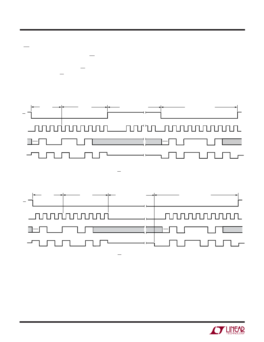
Data transfer is initiated by a falling chip select (CS) signal.
After the falling CS is recognized, an 8-bit input word
is shifted into the D
IN
input which configures the LTC1090
for the next conversion. Simultaneously, the result of the
previous conversion is output on the D
OUT
line. At the end
of the data exchange the requested conversion begins and
CS should be brought high. After t
CONV
, the conversion is
complete and the results will be available on the next data
transfer cycle. As shown below, the result of a conversion
is delayed by one CS cycle from the input word requesting
it.
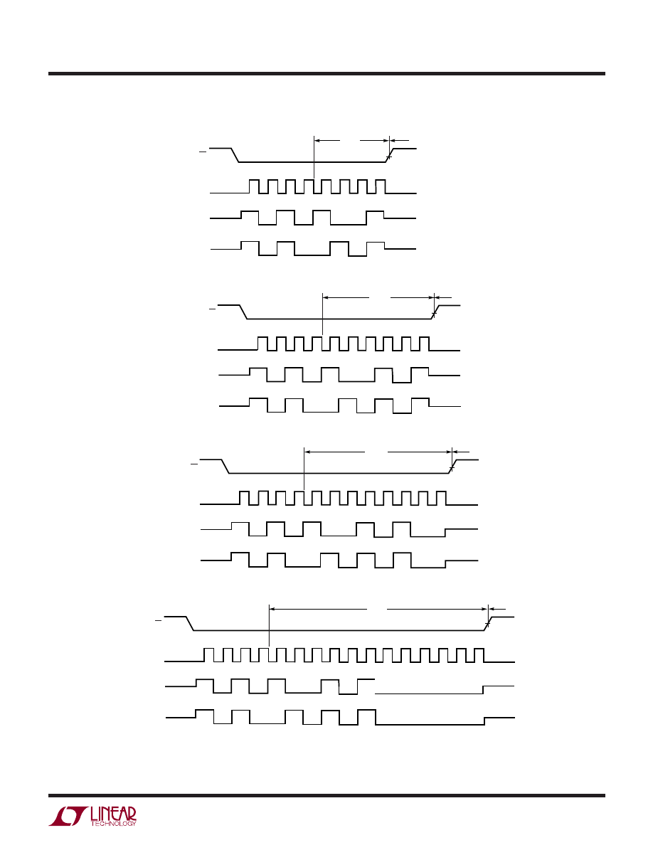
2. Input Data Word
The LTC1090 8-bit input data word is clocked into the D
IN
input on the first eight rising SCLK edges after chip select
is recognized. Further inputs on the D
IN
pin are then
ignored until the next CS cycle. The eight bits of the input
word are defined as follows:
Multiplexer (MLIX) Address
The first four bits of the input word assign the MUX
configuration for the requested conversion. For a given
channel selection, the converter will measure the voltage
between the two channels indicated by the + and – signs
in the selected row of Table 1. Note that in differential
mode (SGL/DIFF = O) measurements are limited to four
adjacent input pairs with either polarity. In single ended
mode, all input channels are measured with respect to
COM. Figure 1 shows some examples of multiplexer
assignments.
Table 1. Multiplexer Channel Selection
MUX ADDRESS
DIFFERENTIAL CHANNEL SELECTION
SGL/
ODD SELECT
DIFF
SIGN
1
0
0
1
2
3
4
5
6
7
0
0
0
0
+
–
0
0
0
1
+
–
0
0
1
0
+
–
0
0
1
1
+
–
0
1
0
0
–
+
0
1
0
1
–
+
0
1
1
0
–
+
0
1
1
1
–
+
MUX ADDRESS
SINGLE ENDED CHANNEL SELECTION
SGL/ ODD/ SELECT
DIFF SIGN
1
0
0
1
2
3
4
5
6
7 COM
1
0
0
0
+
–
1
0
0
1
+
–
1
0
1
0
+
–
1
0
1
1
+
–
1
1
0
0
+
–
1
1
0
1
+
–
1
1
1
0
+
–
1
1
1
1
+
–
APPLICATIO S I FOR ATIO
W
U
U
U
LTC1090 • AI02
Data
Transfer
t
CONV
A/D
Conversion
D
OUT
D
IN
D
IN
Word 1
D
OUT
Word 0
t
CONV
A/D
Conversion
Data
Transfer
D
IN
Word 2
D
OUT
Word 1
D
IN
Word 3
D
OUT
Word 2
LTC1090• AI03
Data Input (D
IN
) Word:
ODD/
SIGN
SELECT
1
SELECT
0
UNI
MSBF
WL1
Word Length
MUX Address
Unipolar/
Bipolar
MSB First/
LSB First
WL0
SGL/
DIFF
11
LTC1090
1090fc
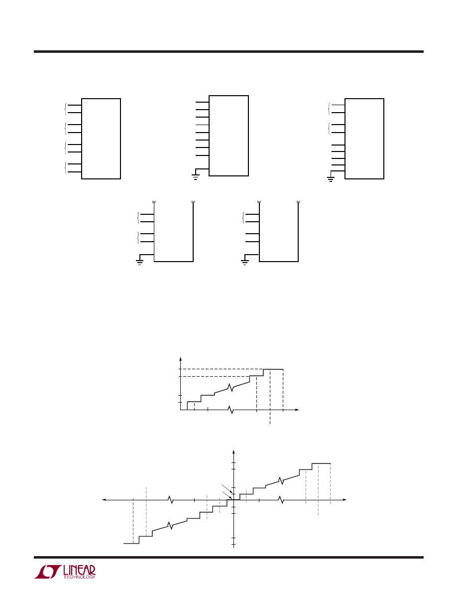
4 Differential
8 Single Ended
Combinations of Differential and Single Ended
Changing the MUX Assignment “On the Fly”
Figure 1. Examples of Multiplexer Options on the LTC1090
Unipolar/Bipolar (UNI)
The fifth input bit (UNI) determines whether the conver-
sion will be unipolar or bipolar. When UNI is a logical one,
a unipolar conversion will be performed on the selected
input voltage. When UNI is a logical zero, a bipolar conver-
sion will result. The input span and code assignment for
each conversion type are shown in the figures below.
Unipolar Transfer Curve (UNI = 1)
Bipolar Transfer Curve (UNI = 0)
APPLICATIO S I FOR ATIO
W
U
U
U
LTC1090 • AI04A
0,1
CHANNEL
2,3
4,5
6,7
+ ( – )
– ( + )
+ ( – )
– ( + )
+ ( – )
– ( + )
+ ( – )
– ( + )
LTC1090 • AI04B
CHANNEL
0
1
2
3
4
5
6
7
COM ( – )
+
+
+
+
+
+
+
+
LTC1090 • AI04C
+
+
+
+
0,1
CHANNEL
2,3
4
5
6
7
+
–
+
–
COM (
–
)
LTC1090 • AI04D
4,5
6,7
–
+
–
+
COM (UNUSED)
1ST CONVERSION
LTC1090 • AI04E
5,4
6
7
–
+
+
+
COM (
–
)
2ND CONVERSION
LTC1090 • AI05
1 1 1 1 1 1 1 1 1 1
1 1 1 1 1 1 1 1 1 0
0 0 0 0 0 0 0 0 0 1
0 0 0 0 0 0 0 0 0 0
OV
1LSB
V
REF
– 2LSB
V
REF
– 1LSB
V
REF
V
IN
LTC1090 • AI06
0 1 1 1 1 1 1 1 1 1
0 1 1 1 1 1 1 1 1 0
1 1 1 1 1 1 1 1 1 1
1 1 1 1 1 1 1 1 1 0
0 0 0 0 0 0 0 0 0 1
0 0 0 0 0 0 0 0 0 0
1 0 0 0 0 0 0 0 0 1
1 0 0 0 0 0 0 0 0 0
V
REF
– 2LSB
– V
REF
+1LSB
V
REF
– 1LSB
V
REF
– V
REF
V
IN
– 2LSB
– 1LSB
1LSB
12
LTC1090
1090fc
Unipolar Output Code (UNI = 1)
INPUT VOLTAGE
OUTPUT CODE
INPUT VOLTAGE
(V
REF
= 5V)
1111111111
V
REF
– 1LSB
4.9951V
1111111110
V
REF
– 2LSB
4.9902V
•
•
•
•
•
•
•
•
•
0000000001
1LSB
0.0049V
0000000000
0V
0V
Bipolar Output Code (UNI = 0)
INPUT VOLTAGE
OUTPUT CODE
INPUT VOLTAGE
(V
REF
= 5V)
0111111111
V
REF
– 1LSB
4.9902V
0111111110
V
REF
– 2LSB
4.9805V
•
•
•
•
•
•
•
•
•
0000000001
1LSB
0.0098V
0000000000
0V
0V
1111111111
–1LSB
–0.0098V
1111111110
–2LSB
–0.0195V
•
•
•
•
•
•
•
•
•
1000000001
– (V
REF
) + 1LSB
–4.9902V
1000000000
– (V
REF
)
–5.000V
MSB First/LSB First Format (MSBF)
The output data of the LTC1090 is programmed for MSB
first or LSB first sequence using the MSBF bit. For MSB
first output data the input word clocked to the LTC1090
should always contain a logical one in the sixth bit location
(MSBF bit). Likewise for LSB first output data, the input
word clocked to the LTC1090 should always contain a zero
in the MSBF bit location. The MSBF bit in a given D
IN
word
will control the order of the next D
OUT
word. The MSBF bit
affects only the order of the output data word. The order
of the input word is unaffected by this bit.
MSBF
OUTPUT FORMAT
0
LSB First
1
MSB First
Word Length (WL1, WL0)
The last two bits of the input word (WL1 and WL0) program
the output data word length of the LTC1090. Word lengths
of 8, 10, 12 or 16 bits can be selected according to the
following table. The WL1 and WL0 bits in a given D
IN
word
control the length of the present, not the next, D
OUT
word.
WL1 and WL0 are never “don’t cares” and must be set for
the correct D
OUT
word length even when a “dummy” D
IN
word is sent. On any transfer cycle, the word length should
be made equal to the number of SCLK cycles sent by the
MPU.
WL1
WL0
OUTPUT WORD LENGTH
0
0
8 Bits
0
1
10 Bits
1
0
12 Bits
1
1
16 Bits
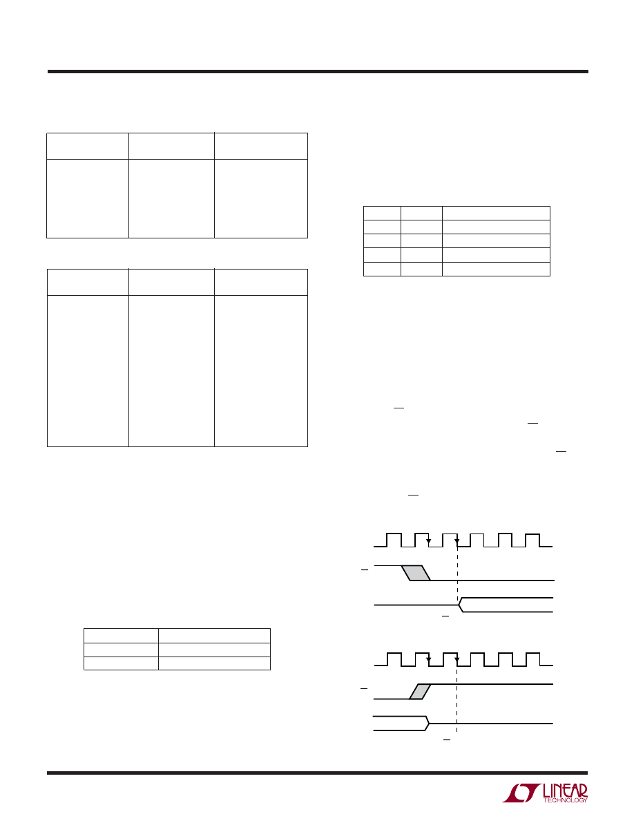
Figure 2 shows how the data output (D
OUT
) timing can be
controlled with word length selection and MSB/LSB first
format selection.
3. Deglitcher
A deglitching circuit has been added to the Chip Select
input of the LTC1090 to minimize the effects of errors
caused by noise on that input. This circuit ignores changes
in state on the CS input that are shorter in duration than 1
ACLK cycle. After a change of state on the CS input, the
LTC1090 waits for two falling edges of the ACLK before
recognizing a valid chip select. One indication of CS low
recognition is the D
OUT
line becoming active (leaving the
Hi-Z state). Note that the deglitching applies to both the
rising and falling CS edges.
APPLICATIO S I FOR ATIO
W
U
U
U
HIGH Z
HIGH Z
ACLK
ACLK
VALID OUTPUT
D
OUT
D
OUT
CS
CS
LOW CS RECOGNIZED
INTERNALLY
HIGH CS RECOGNIZED
INTERNALLY
LTC1090 • AI07
13
LTC1090
1090fc
8-Bit Word Length
10-Bit Word Length
12-Bit Word Length
16-Bit Word Length
Figure 2. Data Output (D
OUT)
Timing with Different Word Lengths
APPLICATIO S I FOR ATIO
W
U
U
U
(SB)
SCLK
D
OUT
MSB FIRST
D
OUT
LSB FIRST
1
8
B9
B8
B7
B6
B5
B4
B3
B0
B1
B2
B3
B4
B5
B6
B2
B7
CS
t
SMPL
t
CONV
THE LAST TWO BITS
ARE TRUNCATED
LTC1090 • AI08A
(SB)
(SB)
SCLK
D
OUT
MSB FIRST
D
OUT
LSB FIRST
1
10
B9
B8
B7
B6
B5
B4
B3
B0
B1
B2
B3
B4
B5
B6
B2
B1
B0
B7
B8
B9
CS
t
SMPL
t
CONV
LTC1090 • AI08B
(SB)
(SB)
SCLK
D
OUT
MSB FIRST
D
OUT
LSB FIRST
1
12
10
B9
B8
B7
B6
B5
B4
B3
B0
B1
B2
B3
B4
B5
B6
B2
B1
B0
B7
B8
B9
CS
t
SMPL
t
CONV
FILL
ZEROES
*
*
LTC1090 • AI08C
(SB)
(SB)
SCLK
D
OUT
MSB FIRST
D
OUT
LSB FIRST
1
16
10
B9
B8
B7
B6
B5
B4
B3
B0
B1
B2
B3
B4
B5
B6
B2
B1
B0
B7
B8
B9
CS
t
SMPL
t
CONV
FILL
ZEROES
*
*
*
*
*
*
*IN UNIPOLAR MODE, THESE BITS ARE FILLED WITH ZEROES.
IN BIPOLAR MODE, THE SIGN BIT IS EXTENDED INTO THESE LOCATIONS
LTC1090 • AI08D
14
LTC1090
1090fc
4. CS Low During Conversion
In the normal mode of operation, CS is brought high
during the conversion time (see Figure 3). The serial port
ignores any SCLK activity while CS is high. The LTC1090
will also operate with CS low during the conversion. In this
mode, SCLK must remain low during the conversion as
shown in Figure 4. After the conversion is complete, the
D
OUT
line will become active with the first output bit. Then
the data transfer can begin as normal.
5. Microprocessor Interfaces
The LTC1090 can interface directly (without external hard-
ware) to most popular microprocessor (MPU) synchronous
Figure 3. CS High During Conversion
Figure 4. CS Low During Conversion
APPLICATIO S I FOR ATIO
W
U
U
U
LTC1090 • AI09
B9
SHIFT RESULT OUT
AND NEW ADDRESS IN
B8
B7
B6
B5
B4
B3
B2
B1
B0
B9
B8
B7
B6
B5
B4
B3
B2
B1
B0
ODD/
SIGN
SGL/
DIFF
SEL
1
D
OUT
SCLK
SEL
0
UNI MSBF WL1 WL0
ODD/
SIGN
SGL/
DIFF
SEL
1
SEL
0
UNI MSBF WL1 WL0
t
SMPL
SAMPLE
ANALOG
INPUT
40 TO 44 ACLK CYCLES
SHIFT
MUX
ADDRESS
IN
D
IN
CS
DON’T CARE
LTC1090 • AI10
B9
SHIFT RESULT OUT
AND NEW ADDRESS IN
B8
B7
B6
B5
B4
B3
B2
B1
B0
B9
B8
B7
B6
B5
B4
B3
B2
B1
B0
ODD/
SIGN
SGL/
DIFF
SEL
1
SCLK
D
OUT
SEL
0
UNI MSBF WL1 WL0
ODD/
SIGN
SGL/
DIFF
SEL
1
SEL
0
UNI MSBF WL1 WL0
t
SMPL
SAMPLE
ANALOG
INPUT
40 TO 44 ACLK CYCLES
SCLK MUST REMAIN LOW
SHIFT
MUX
ADDRESS
IN
D
IN
CS
DON’T CARE
15
LTC1090
1090fc
serial formats (see Table 2). If an MPU without a serial
interface is used, then 4 of the MPU’s parallel port lines can
be programmed to form the serial link to the LTC1090.
Included here are three serial interface examples and one
example showing a parallel port programmed to form the
serial interface.
Table 2. Microprocessors with Hardware Serial Interfaces
Compatible with the LTC1090**
PART NUMBER
TYPE OF INTERFACE
Motorola
MC6805S2, S3
SPI
MC68HC11
SPI
MC68HC05
SPI
RCA
CDP68HC05
SPI
Hitachi
HD6305
SCI Synchronous
HD63705
SCI Synchronous
HD6301
SCI Synchronous
HD63701
SCI Synchronous
HD6303
SCI Synchronous
National Semiconductor
COP400 Family
MICROWIRE
†
COP800 Family
MICROWIRE/PLUS
†
NS8050U
MICROWIRE/PLUS
HPC16000 Family
MICROWIRE/PLUS
Texas Instruments
TMS7002
Serial Port
TMS7042
Serial Port
TMS70C02
Serial Port
TMS70C42
Serial Port
TMS32011*
Serial Port
TMS32020*
Serial Port
*Requires external hardware
**Contact LTC Marketing for interface information for processors not on
this list
†
MICROWIRE and MlCROWIRE/PLUS are trademarks of National
Semiconductor Corp.
Serial Port Microprocessors
Most synchronous serial formats contain a shift clock
(SCLK) and two data lines, one for transmitting and one for
receiving. In most cases data bits are transmitted on the
falling edge of the clock (SCLK) and captured on the rising
edge. However, serial port formats vary among MPU
manufacturers as to the smallest number of bits that can
be sent in one group (e.g., 4-bit, 8-bit or 16-bit transfers).
They also vary as to the order in which the bits are
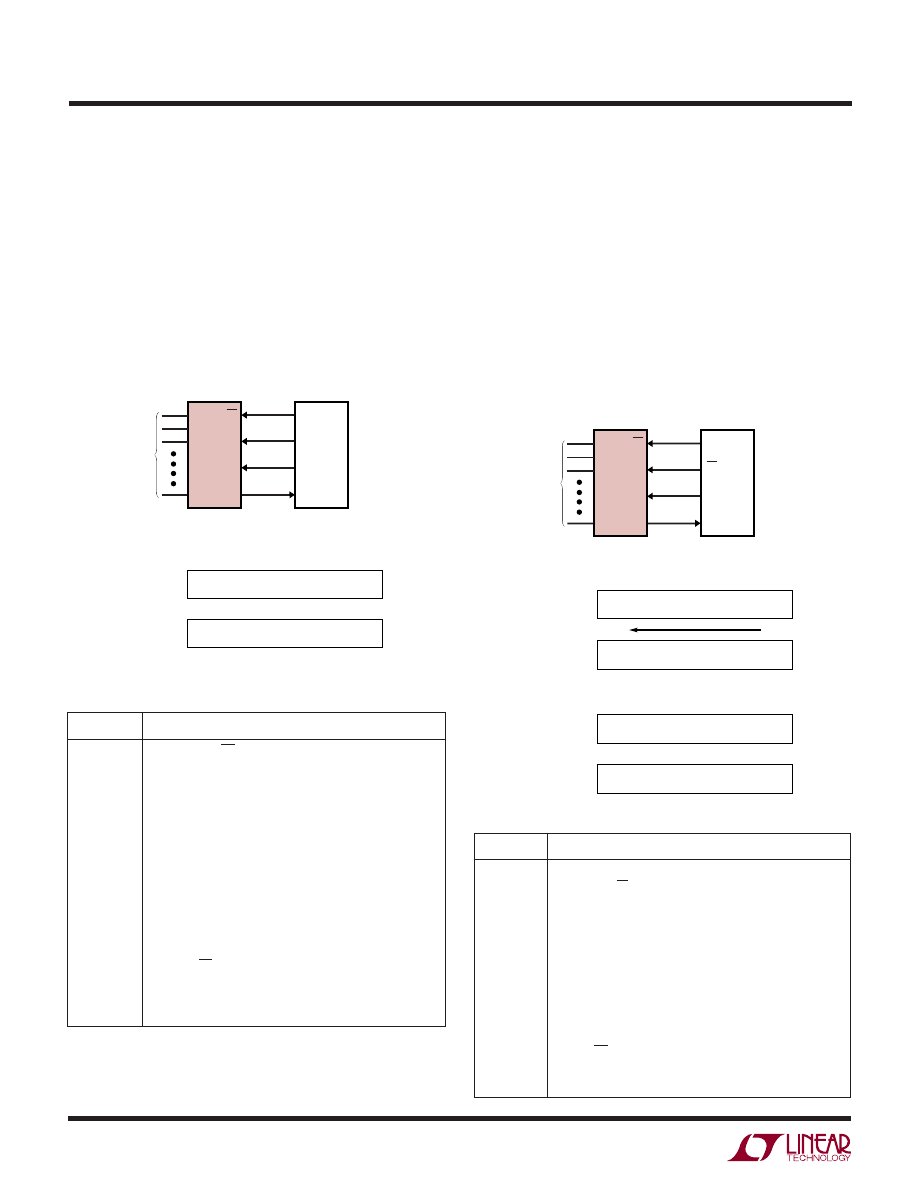
transmitted (LSB or MSB first). The following examples
show how the LTC1090 accommodates these differences.
National MICROWIRE (COP420)
The COP420 transfers data MSB first and in 4-bit incre-
ments (nibbles). This is easily accommodated by setting
the LTC1090 to MSB first format and 12-bit word length.
The data output word is then received by the COP420 in
three 4-bit blocks with the final two unused bits filled with
zeroes by the LTC1090.
Hardware and Software Interface to National Semiconductor
COP420 Processor
APPLICATIO S I FOR ATIO
W
U
U
U
MNEMONIC
DESCRIPTION
LEI
Enable SlO
SC
Set Carry flag
OGI
G0 is set to (CS goes low)
LDD
Load first 4 bits of D
IN
to ACC
XAS
Swap ACC with SIO reg. Starts SK Clk
LDD
Load 2nd 4 bits of D
IN
to ACC
NOP
Timing
XAS
Swap first 4 bits from A/D with ACC. SK continues.
XIS
Put first 4 bits in RAM (location A)
NOP
Timing
XAS
Swap 2nd 4 bits from A/D with ACC. SK continues.
XIS
Put 2nd 4 bits in RAM (location A + 1)
RC
Clear Carry
NOP
Timing
XAS
Swap 3rd 4 bits from A/D with ACC. SK off
XIS
Put 3rd 4 bits in RAM (location A + 2)
OGI
G0 is set to 1 (CS goes high)
LEI
Disable SlO
LTC1090
ANALOG
INPUTS
D
OUT
D
OUT
from LTC1090 stored in COP420 RAM
D
IN
SCLK
GO
SK
SO
SI
COP420
CS
B9
Location A
Location A + 1
first 4 bits
second 4 bits
third 4 bits
LSB
MSB*
B8 B7 B6
B5 B4 B3 B2
Location A + 2
B1 B0 B0 B0
LTC1090 • AI11
*B9 is MSB in unipolar or sign bit in bipolar
16
LTC1090
1090fc
Motorola SPI (MC68HC05C4)
The MC68HC05C4 transfers data MSB first and in 8-bit
increments. Programming the LTC1090 for MSB first
format and 16-bit word length allows the 10-bit data
output to be received by the MPU as two 8-bit bytes with
the final 6 unused bits filled with zeroes by the LTC1090.
Hardware and Software Interface to Motorola MC68HC05C4
Processor
Hitachi Synchronous SCI (HD63705)
The HD63705 transfers serial data in 8-bit increments,
LSB first. To accommodate this, the LTC1090 is
programmed for 16-bit word length and LSB first format.
The 10-bit output data is received by the processor as two
8-bit bytes, LSB first. The LTC1090 fills the final 6 unused
bits (after the MSB) with zeroes in unipolar mode and with
the sign bit in bipolar mode.
Hardware and Software Interface to Hitachi HD63705 Processor
APPLICATIO S I FOR ATIO
W
U
U
U
MNEMONIC
DESCRIPTION
BCLR n
C0 is cleared (CS goes Low)
LDA
Load D
IN
for LTC1090 into ACC
STA
Load D
IN
from ACC to SPI data reg. Start SCK
↑
NOP
8 NOPs for timing
↓
LDA
Load contents of SPI status reg. into ACC
LDA
Load LTC1090 D
OUT
from SPI data reg. into ACC (byte 1)
STA
Load LTC1090 D
OUT
into RAM (location A)
STA
Start next SPl cycle
↑
NOP
6 NOPs for timing
↓
BSET n
C0 is set (CS goes high)
LDA
Load contents of SPI status reg. into ACC
LDA
Load LTC1090 D
OUT
from SPI data reg. into ACC (byte 2)
STA
Load LTC1090 D
OUT
into RAM (location A + 1)
LTC1090
ANALOG
INPUTS
D
OUT
D
OUT
from LTC1090 stored in MC68HCO5C4 RAM
D
IN
SCLK
CO
SCK
MOSI
MISO
MC68HCO5C4
CS
B9
Location A
Location A + 1
byte 1
byte 2
*B9 is MSB in unipolar or sign bit in bipolar
MSB*
LSB
B8 B7 B6 B5 B4 B3 B2
B1 B0
0
0
0
0
0
0
LTC1090 • AI12
MNEMONIC
DESCRIPTION
LDA
Load D
IN
word for LTC1090 into ACC from RAM
BCLR n
C0 cleared (CS goes low)
STA
Load D
IN
word for LTC1090 into SCI data reg. from ACC
and start clocking data (LSB first)
↑
NOP
6 NOPs for timing
↓
LDA
Load contents of SCI data reg. into ACC (byte 1)
Start next SCI cycle
STA
Load LTC1090 D
OUT
word into RAM (Location A)
NOP
Timing
BSET n
C0 set (CS goes high)
LDA
Load contents of SCI data reg. into ACC (byte 2)
STA
Load LTC1090 D
OUT
word into RAM (Location A + 1)
LTC1090
ANALOG
INPUTS
D
OUT
D
OUT
from LTC1090 stored in HD63705 RAM
D
IN
SCLK
C0
CK
T
X
R
X
HD63705
CS
B7
Location A
Location A + 1
Bipolar
Sign
byte 1
byte 2
LSB
B6 B5 B4 B3 B2 B1 B0
B9 B9 B9 B9 B9 B9 B9 B8
LTC1090 • AI13
B7
Location A
Location A + 1
Unipolar
byte 1
byte 2
LSB
MSB
B6 B5 B4 B3 B2 B1 B0
0
0 0
0
0
0 B9 B8
17
LTC1090
1090fc
Parallel Port Microprocessors
When interfacing the LTC1090 to an MPU which has a
parallel port, the serial signals are created on the port with
software. Three MPU port lines are programmed to create
the CS, SCLK and D
IN
signals for the LTC1090. A fourth
port line reads the D
OUT
line. An example is made of the
Intel 8051/8052/80C252 family.
Intel 8051
To interface to the 8051, the LTC1090 is programmed for
MSB first format and 10-bit word length. The 8051 gener-
ates CS, SCLK and D
IN
on three port lines and reads D
OUT
on the fourth.
Hardware and Software Interface to Intel 8051 Processor
8051 Code
MNEMONIC
DESCRIPTION
MOV PI,#02H
Initialize port 1 (bit 1 is made
an input)
CLR P1.3
SCLK goes low
SETB P1.4
CS goes high
CONTINUE: MOV A,#0DH
D
IN
word for the LTC1090 is
placed in ACC.
CLR P1.4
CS goes low
MOV R4,#08
Load counter
NOP
Delay for deglitcher
LOOP:
MOV C, P1.1
Read data bit into carry
RLC A
Rotate data bit into ACC
MOV P1.2, C
Output D
IN
bit to LTC1090
SETB P1.3
SCLK goes high
CLR P1.3
SCLK goes low
DJNZ R4, LOOP
Next bit
MOV R2, A
Store MSBs in R2
MOV C, P1.1
Read data bit into carry
CLR A
CIear ACC
RLC A
Rotate data bit into ACC
SETB P1.3
SCLK goes high
CLR P1.3
SCLK goes low
MOV C, P1.1
Read data bit into carry
RRC A
Rotate right into ACC
RRC A
Rotate right into ACC
MOV R3, A
Store LSBs in R3
SETB P1.3
SCLK goes high
CLR P1.3
SCLK goes low
SETB P1.4
CS goes high
MOV R5,#07H
Load counter
DELAY:
DJNZ R5, DELAY
Delay for LTC1090 to perform
conversion
AJMP CONTINUE
Repeat program
APPLICATIO S I FOR ATIO
W
U
U
U
Figure 5. Several LTC1090’s Sharing One 3-Wire Serial Interface
LTC1090
ANALOG
INPUTS
D
OUT
D
OUT
from LTC1090 stored in 8051 RAM
D
IN
SCLK
ACLK
CS
P1.1
P1.2
P1.3
ALE
P1.4
8051
B9
R2
R3
*B9 is MSB in unipolar or sign bit in bipolar
MSB*
LSB
B8 B7 B6 B5 B4 B3 B2
B1 B0
0
0
0
0
0
0
LTC1090 • AI14
LTC1090
3
3
2 1 0
CS
8 CHANNELS
OUTPUT PORT
SERIAL DATA
3-WIRE SERIAL
INTERFACE TO OTHER
PERIPHERALS OR LTC1090s
MPU
LTC1090
3
CS
8 CHANNELS
LTC1090
3
CS
8 CHANNELS
18
LTC1090
1090fc
6. Sharing the Serial Interface
The LTC1090 can share the same 3-wire serial interface
with other peripheral components or other LTC1090s (see
Figure 5). In this case, the CS signals decide which
LTC1090 is being addressed by the MPU.
ANALOG CONSIDERATIONS
1. Grounding
The LTC1090 should be used with an analog ground plane
and single point grounding techniques.
Pin 11 (AGND) should be tied directly to this ground plane.
Pin 10 (DGND) can also be tied directly to this ground
plane because minimal digital noise is generated within
the chip itself.
Pin 20 (V
CC
) should be bypassed to the ground plane with
a 4.7µF tantalum with leads as short as possible. Pin 12
(V
–
) should be bypassed with a 0.1µF ceramic disk. For
single supply applications, V
–
can be tied to the ground
plane.
It is also recommended that pin 13 (REF
–
) and pin 9 (COM)
be tied directly to the ground plane. All analog inputs
should be referenced directly to the single point ground.
Digital inputs and outputs should be shielded from and/or
routed away from the reference and analog circuitry.
Figure 6 shows an example of an ideal ground plane design
for a two sided board. Of course this much ground plane
will not always be possible, but users should strive to get
as close to this ideal as possible.
2. Bypassing
For good performance, V
CC
must be free of noise and
ripple. Any changes in the V
CC
voltage with respect to
analog ground during a conversion cycle can induce
errors or noise in the output code. V
CC
noise and ripple can
be kept below 1mV by bypassing the V
CC
pin directly to the
analog ground plane with a 4.7µF tantalum with leads as
short as possible. Figures 7 and 8 show the effects of good
and poor V
CC
bypassing.
APPLICATIO S I FOR ATIO
W
U
U
U
Figure 7. Poor V
CC
Bypassing. Noise and Ripple
can Cause A/D Errors
Figure 6. Example Ground Plane for the LTC1090
HORIZONTAL: 10µs/DIV
VERTICAL: 0.5mV/DIV
Figure 8. Good V
CC
Bypassing Keeps Noise and Ripple
on V
CC
Below 1mV
HORIZONTAL: 10µs/DIV
VERTICAL: 0.5mV/DIV
20
V
CC
V –
10
11
LTC1090 • AI15
ANALOG
GROUND
PLANE
0.1µF CERAMIC DISK
4.7µF TANTALUM
1
19
LTC1090
1090fc
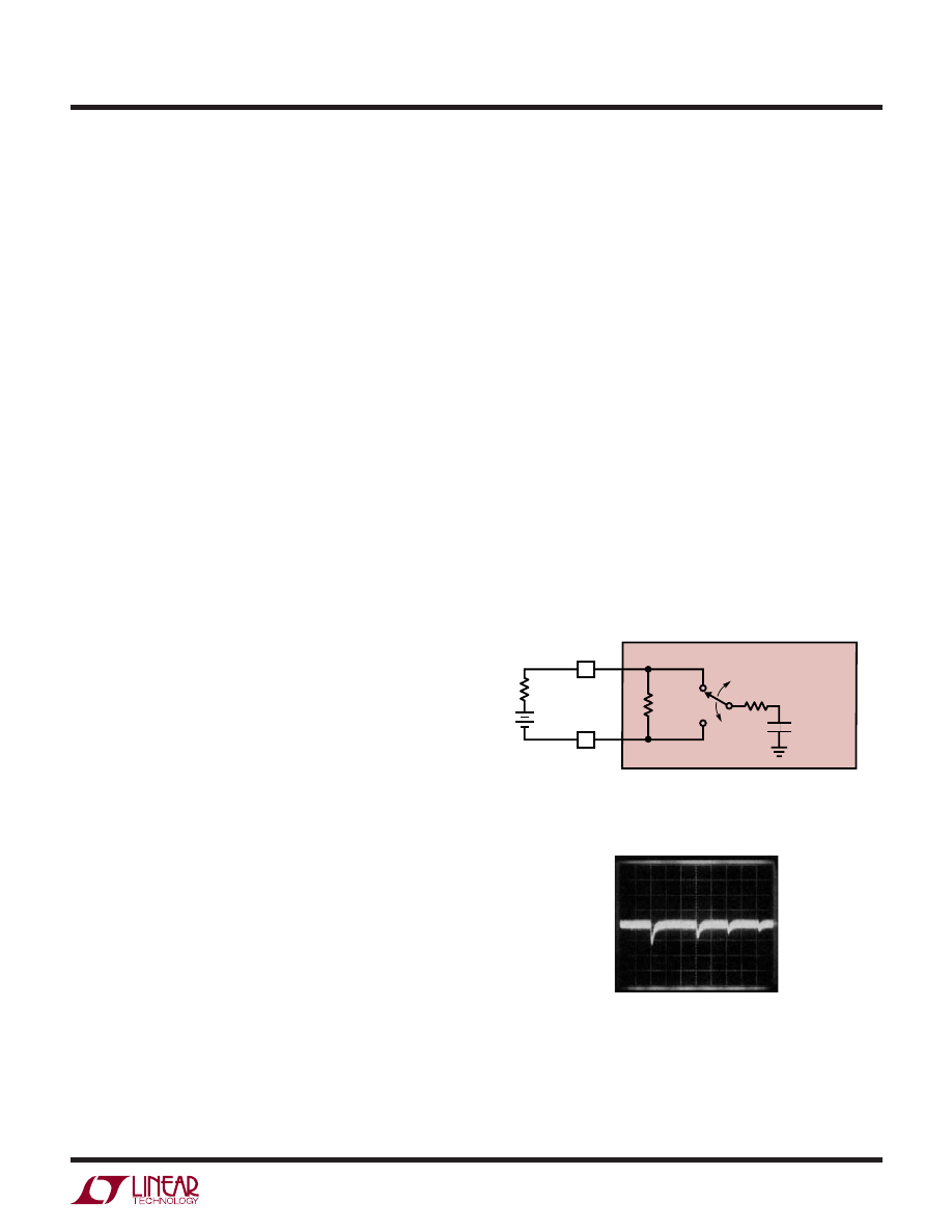
3. Analog Inputs
Because of the capacitive redistribution A/D conversion
techniques used, the analog inputs of the LTC1090 have
capacitive switching input current spikes. These current
spikes settle quickly and do not cause a problem.
However, if large source resistances are used or if slow
settling op amps drive the inputs, care must be taken to
insure that the transients caused by the current spikes
settle completely before the conversion begins.
Source Resistance
The analog inputs of the LTC1090 look like a 60pF capaci-
tor (C
IN
) in series with a 500Ω resistor (R
ON
) as shown in
Figure 9. C
IN
gets switched between the selected “+” and
“–” inputs once during each conversion cycle. Large
external source resistors and capacitances will slow the
settling of the inputs. It is important that the overall RC
time constants be short enough to allow the analog inputs
to completely settle within the allowed time.
APPLICATIO S I FOR ATIO
W
U
U
U
Figure 9. Analog Input Equivalent Circuit
“+” Input Settling
This input capacitor is switched onto the “+” input during
the sample phase (t
SMPL
, see Figure 10). The sample
phase starts at the 4th SCLK cycle and lasts until the falling
edge of the last SCLK (the 8th, 10th, 12th or 16th SCLK
cycle depending on the selected word length). The voltage
on the “+” input must settle completely within this sample
time. Minimizing R
SOURCE
+
and C1 will improve the input
settling time. If large “+” input source resistance must be
used, the sample time can be increased by using a slower
SCLK frequency or selecting a longer word length. With
the minimum possible sample time of 4µs, R
SOURCE
+
< 2k
and C1 < 20pF will provide adequate settling.
“–” Input Settling
At the end of the sample phase the input capacitor switches
to the “–” input and the conversion starts (see Figure 10).
During the conversion, the “+” input voltage is effectively
“held” by the sample and hold and will not affect the
conversion result. However, it is critical that the “–” input
voltage be free of noise and settle completely during the
first four ACLK cycles of the conversion time. Minimizing
R
SOURCE
–
and C2 will improve settling time. If large
“–” input source resistance must be used, the time allowed
for settling can be extended by using a slower ACLK
frequency. At the maximum ACLK rate of 2MHz, R
SOURCE
–
< 1kΩ and C2 < 20pF will provide adequate settling.
Figure 10. “+” and “–” Input Settling Windows
LTC1090 • AI17
CS
SCLK
ACLK
t
SMPL
HOLD
1
1ST BIT
TEST
LAST SCLK (8TH, 10TH, 12TH OR 16TH DEPENDING ON WORK LENGTH)
“ – ” INPUT MUST SETTLE
DURING THIS TIME
“ + ” INPUT MUST
SETTLE DURING THIS TIME
2
3
4
1
2
3
4
SAMPLE
MUX ADDRESS
SHIFTED IN
“ – ” INPUT
“ + ” INPUT
LTC1090 • AI16
R
SOURCE
+
R
SOURCE
–
V
IN
–
V
IN
+
4TH SCLK
LAST SCLK
R
ON
= 500Ω
C
IN
= 60pF
LTC1090
“
–
”
INPUT
C1
C2
“
+
”
INPUT
20
LTC1090
1090fc
Input Op Amps
When driving the analog inputs with an op amp it is
important that the op amp settle within the allowed time
(see Figure 10). Again, the “+” and “–” input sampling
times can be extended as described above to accommo-
date slower op amps. Most op amps including the LT1006
and LT1013 single supply op amps can be made to settle
well even with the minimum settling windows of 4µs (“+”
input) and 2µs (“–” input) which occur at the maximum
clock rates (ACLK = 2MHz and SCLK = 1MHz). Figures 11
and 12 show examples of adequate and poor op amp
settling.
RC Input Filtering
It is possible to filter the inputs with an RC network as
shown in Figure 13. For large values of C
F
(e.g., 1µF), the
capacitive input switching currents are averaged into a net
DC current. Therefore, a filter should be chosen with a
small resistor and large capacitor to prevent DC drops
across the resistor. The magnitude of the DC current is
approximately l
DC
= 60pF x V
IN
/t
CYC
and is roughly propor-
tional to V
IN
. When running at the minimum cycle time of
33µs, the input current equals 9µA at V
IN
= 5V. In this case,
a filter resistor of 50Ω will cause 0.1LSB of full-scale error.
If a larger filter resistor must be used, errors can be
eliminated by increasing the cycle time as shown in the
typical curve of Maximum Filter Resistor vs Cycle Time.
Figure 11. Adequate Settling of Op Amp Driving Analog Input
Figure 12. Poor Op Amp Settling can Cause A/D Errors
Figure 13. RC Input Filtering
APPLICATIO S I FOR ATIO
W
U
U
U
HORIZONTAL: 1µs/DIV
VERTICAL: 5mV/DIV
HORIZONTAL: 20µs/DIV
VERTICAL: 5mV/DIV
LTC1090 • AI18
V
IN
R
FILTER
I
DC
C
FILTER
LTC1090
“ + ”
“ – ”
Input Leakage Current
Input leakage currents can also create errors if the source
resistance gets too large. For instance, the maximum input
leakage specification of 1µA (at 125°C) flowing through a
source resistance of 1kΩ will cause a voltage drop of 1mV
or 0.2LSB. This error will be much reduced at lower
temperatures because leakage drops rapidly (see typical
curve of Input Channel Leakage Current vs Temperature).
Noise Coupling into Inputs
High source resistance input signals (>500Ω) are more
sensitive to coupling from external sources. It is preferable
to use channels near the center of the package (i.e., CH2 to
CH7) for signals which have the highest output resistance
because they are essentially shielded by the pins on the
package ends (DGND and CH0). Grounding any unused
inputs (especially the end pin, CH0) will also reduce
outside coupling into high source resistances.
4. Sample-and-Hold
Single Ended Inputs
The LTC1090 provides a built-in sample and hold (S&H)
function for all signals acquired in the single ended mode
(COM pin grounded). This sample and hold allows the
LTC1090 to convert rapidly varying signals (see typical
curve of S&H Acquisition Time vs Source Resistance). The
input voltage is sampled during the t
SMPL
time as shown
in Figure 10. The sampling interval begins after the fourth
21
LTC1090
1090fc
MUX address bit is shifted in and continues during the
remainder of the data transfer. On the falling edge of the
final SCLK, the S&H goes into hold mode and the conver-
sion begins. The voltage will be held on either the 8th,
10th, 12th or 16th falling edge of the SCLK depending on
the word length selected.
Differential Inputs
With differential inputs or when the COM pin is not tied to
ground, the A/D no longer converts just a single voltage
but rather the difference between two voltages. In these
cases, the voltage on the selected “+” input is still sampled
and held and therefore may be rapidly time varying just as
in single ended mode. However, the voltage on the se-
lected “–” input must remain constant and be free of noise
and ripple throughout the conversion time. Otherwise, the
differencing operation may not be performed accurately.
The conversion time is 44 ACLK cycles. Therefore, a
change in the “–” input voltage during this interval can
“–” input this error would be:
V
ERROR (MAX)
= V
PEAK
x 2 x π x f(“–”) x 44/f
ACLK
Where f(“–”) is the frequency of the “–” input voltage,
V
PEAK
is its peak amplitude and f
ACLK
is the frequency of
the ACLK. In most cases V
ERROR
will not be significant. For
a 60Hz signal on the “–” input to generate a 1/4LSB error
(1.25mV) with the converter running at ACLK = 2MHz, its
peak value would have to be 150mV.
5. Reference Inputs
The voltage between the reference inputs of the LTC1090
defines the voltage span of the A/D converter. The refer-
ence inputs look primarily like a 10kΩ resistor but will
have transient capacitive switching currents due to the
switched capacitor conversion technique (see Figure 14).
During each bit test of the conversion (every 4 ACLK
cycles), a capacitive current spike will be generated on the
reference pins by the A/D. These current spikes settle
quickly and do not cause a problem. However, if slow
settling circuitry is used to drive the reference inputs, care
must be taken to insure that transients caused by these
current spikes settle completely during each bit test of the
conversion.
When driving the reference inputs, three things should be
kept in mind:
1. The source resistance (R
OUT
) driving the reference
inputs should be low (less than 1Ω) to prevent DC
drops caused by the 1mA maximum reference current
(I
REF
).
2. Transients on the reference inputs caused by the
capacitive switching currents must settle completely
during each bit test (each 4 ACLK cycles). Figures 15
and 16 show examples of both adequate and poor
settling. Using a slower ACLK will allow more time for
the reference to settle. However, even at the maximum
ACLK rate of 2MHz most references and op amps can
be made to settle within the 2µs bit time.
3. It is recommended that the REF
–
input be tied directly
to the analog ground plane. If REF
–
is biased at a voltage
other than ground, the voltage must not change during
a conversion cycle. This voltage must also be free of
noise and ripple with respect to analog ground.
Figure 14. Reference Input Equivalent Circuit
Figure 15. Adequate Reference Settling
HORIZONTAL: 1µs/DIV
VERTICAL: 0.5mV/DIV
APPLICATIO S I FOR ATIO
W
U
U
U
LTC1090 • AI19
R
OUT
REF
+
REF
–
V
REF
EVERY 4 ACLK CYCLES
10k
TYP
R
ON
5pF – 30pF
LTC1090
14
13

22
LTC1090
1090fc
6. Reduced Reference Operation
The effective resolution of the LTC1090 can be increased
by reducing the input span of the converter. The LTC1090
exhibits good linearity and gain over a wide range of
reference voltages (see typical curves of Linearity and
Gain Error vs Reference Voltage). However, care must be
taken when operating at low values of V
REF
because of the
reduced LSB step size and the resulting higher accuracy
requirement placed on the converter. The following factors
must be considered when operating at low V
REF
values:
1. Conversion speed (ACLK frequency)
2. Offset
3. Noise
Conversion Speed with Reduced V
REF
With reduced reference voltages, the LSB step size is
reduced and the LTC1090 internal comparator overdrive is
reduced. With less overdrive, more time is required to
perform a conversion. Therefore, the maximum ACLK
frequency should be reduced when low values of V
REF
are
used. This is shown in the typical curve of Maximum
Conversion Clock Rate vs Reference Voltage.
Offset with Reduced V
REF
The offset of the LTC1090 has a larger effect on the output
code when the A/D is operated with reduced reference
voltage. The offset (which is typically a fixed voltage)
becomes a larger fraction of an LSB as the size of the LSB
is reduced. The typical curve of Unadjusted Offset Error vs
Reference Voltage shows how offset in LSBs is related to
reference voltage for a typical value of V
OS
. For example,
a V
OS
of 0.5mV which is 0.1LSB with a 5V reference
becomes 0.5LSB with a 1V reference and 2.5LSBs with a
0.2V reference. If this offset is unacceptable, it can be
corrected digitally by the receiving system or by offsetting
the “–” input to the LTC1090.
Noise with Reduced V
REF
The total input referred noise of the LTC1090 can be
reduced to approximately 200µV peak-to-peak using a
ground plane, good bypassing, good layout techniques
and minimizing noise on the reference inputs. This noise
is insignificant with a 5V reference but will become a larger
fraction of an LSB as the size of the LSB is reduced. The
typical curve of Noise Error vs Reference Voltage shows
the LSB contribution of this 200µV of noise.
For operation with a 5V reference, the 200µV noise is only
0.04LSB peak-to-peak. In this case, the LTC1090 noise
will contribute virtually no uncertainty to the output code.
However, for reduced references, the noise may become
a significant fraction of an LSB and cause undesirable jitter
in the output code. For example, with a 1V reference, this
same 200µV noise is 0.2LSB peak-to-peak. This will
reduce the range of input voltages over which a stable
output code can be achieved by 0.2LSB. If the reference is
further reduced to 200mV, the 200µV noise becomes
equal to one LSB and a stable code may be difficult to
achieve. In this case averaging readings may be necessary.
This noise data was taken in a very clean setup. Any setup
induced noise (noise or ripple on V
CC
, V
REF
, V
IN
or V
–
) will
add to the internal noise. The lower the reference voltage
to be used, the more critical it becomes to have a clean,
noise-free setup.
Figure 16. Poor Reference Settling Can Cause A/D Errors
HORIZONTAL: 1µs/DIV
VERTICAL: 0.5mV/DIV
APPLICATIO S I FOR ATIO
W
U
U
U
23
LTC1090
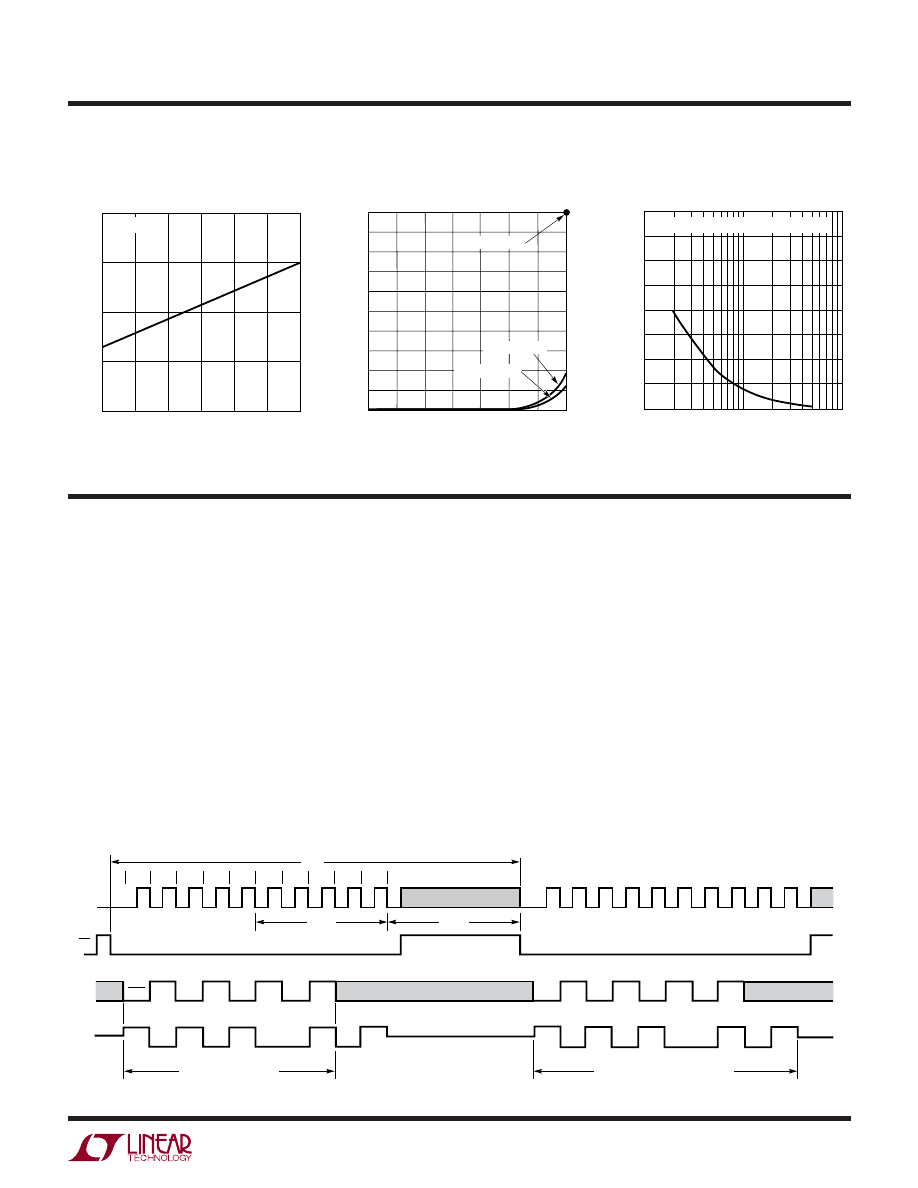
1090fc
SNEAK-A-BIT
TM
The LTC1090’s unique ability to software select the polar-
ity of the differential inputs and the output word length is
used to achieve one more bit of resolution. Using the
circuit below with two conversions and some software, a
2’s complement 10-bit + sign word is returned to memory
inside the MPU. The MC68HC05C4 was chosen as an
example; however, any processor could be used.
Two 10-bit unipolar conversions are performed: the first
over a 0 to 5V span and the second over a 0 to –5V span
(by reversing the polarity of the inputs). The sign of the
input is determined by which of the two spans contained
it. Then the resulting number (ranging from –1023 to 1023
decimal) is converted to 2’s complement notation and
stored in RAM.
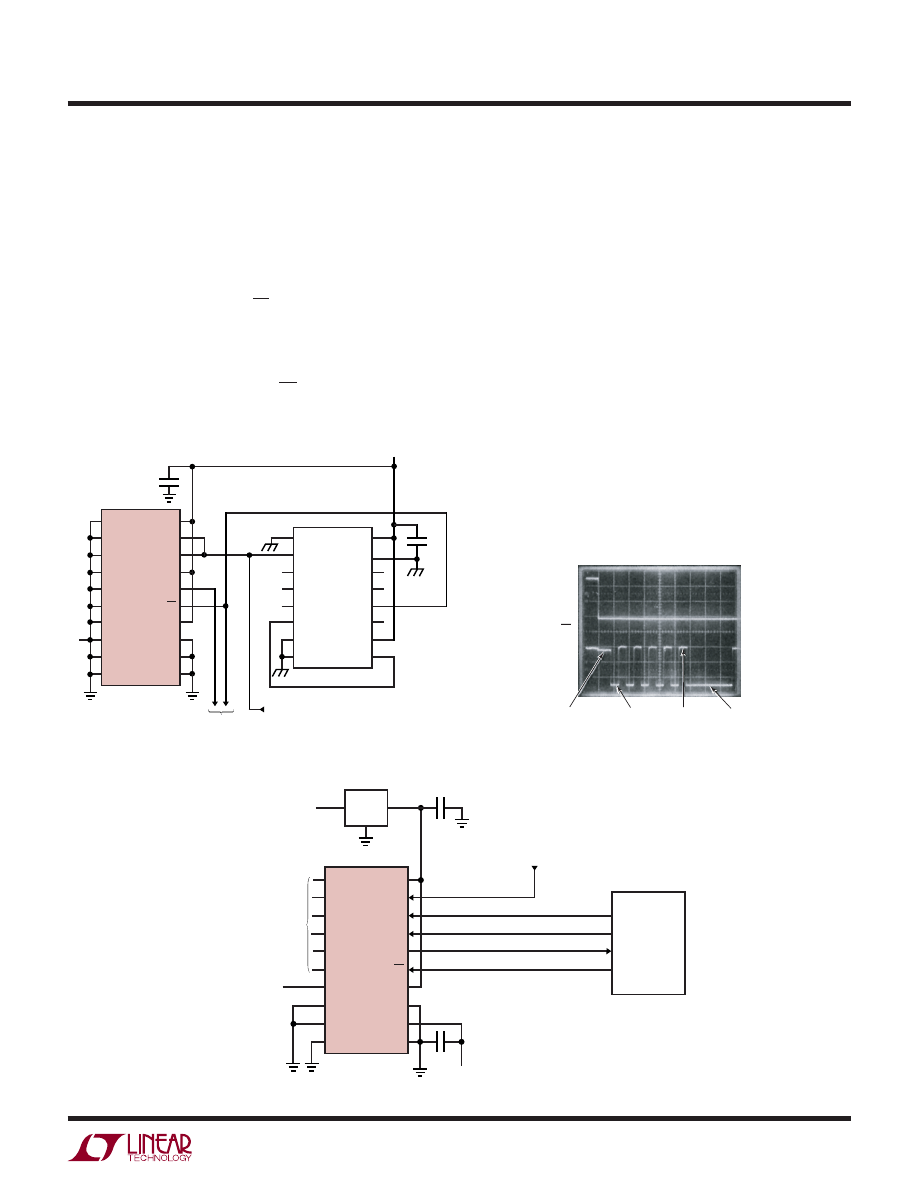
A “Quick Look” Circuit for the LTC1090
Scope Trace of LTC1090 “Quick Look” Circuit
Showing A/D Output of 0101010101 (155
HEX
)
A “Quick Look” Circuit for the LTC1090
Users can get a quick look at the function and timing of the
LTC1090 by using the following simple circuit. REF
+
and
D
IN
are tied to V
CC
selecting a 5V input span, CH7 as a
single ended input, unipolar mode, MSB first format and
16-bit word length. ACLK and SCLK are tied together and
driven by an external clock. CS is driven at 1/64 the clock
rate by the CD4520 and D
OUT
outputs the data. All other
pins are tied to a ground plane. The output data from the
D
OUT
pin can be viewed on an oscilloscope which is set up
to trigger on the falling edge of CS.
U
TYPICAL APPLICATIO
SNEAK-A-BIT Circuit
SNEAK-A-BIT is a trademark of Linear Technology Corp.
LTC1090 • TA04
10µF
9V
V
IN
– 5V TO 5V
OTHER CHANNELS
OR SNEAK-A-BIT
INPUTS
CH0
CH1
CH2
CH3
CH4
CH5
SCK
MOSI
MISO
CO
CH6
CH7
0.1µF
–5V
COM
DGND
V
CC
ACLK
SCLK
D
IN
D
OUT
REF
+
REF
–
V
–
AGND
LTC1090
MC68HC05C4
2MHz
CLOCK
CS
LT1021-5
CS
DOUT
DEGLITCHER
TIME
MSB
(B9)
LSB
(B0)
FILLS
ZERO
LTC1090 • TA03
CH0
CH1
CH2
CH3
CH4
CH5
CH6
CH7
COM
DGND
V
CC
ACLK
SCLK
D
IN
D
OUT
REF
+
REF
–
V
–
AGND
LTC1090
CS
CLK
EN
f/64
5V
4.7µF
f
Q1
Q2
Q3
Q4
RESET
0.1
RESET
Q4
Q3
V
SS
V
IN
V
DD
Q1
EN
CLK
LTC1090
Q2
CLOCK IN
1MHz MAX
TO OSCILLOSCOPE
24
LTC1090
1090fc
U
TYPICAL APPLICATIO
Sneak-A-Bit Code for the LTC1090 Using the MC68HC05C4
MNEMONIC
DESCRIPTION
READ–/+: LDA
#$3F
Load D
IN
word for LTC1090 into ACC
JSR
TRANSFER Read LTC1090 routine
LDA
$60
Load MSBs from LTC1090 into ACC
STA
$71
Store MSBs in $71
LDA
$61
Load LSBs from LTC1090 into ACC
STA
$72
Store LSBs in $72
RTS
Return
READ+/–: LDA
#$7F
Load D
IN
word for LTC1090 into ACC
JSR
TRANSFER Read LTC1090 routine
LDA
$60
Load MSBs from LTC1090 into ACC
STA
$73
Store MSBs in $73
LDA
$61
Load LSBs from LTC1090 into ACC
STA
$74
Store LSBs in $74
RTS
Return
TRANSFER: BCLR 0, $02
CS goes low
STA
$0C
Load D
IN
into SPI. Start transfer
LOOP 1:
TST
$0B
Test status of SPlF
BPL
LOOP 1
Loop to previous instruction if not done
LDA
$0C
Load contents of SPI data reg into ACC
STA
$0C
Start next cycle
STA
$60
Store MSBs in $60
LOOP 2:
TST
$0B
Test status of SPlF
BPL
LOOP 2
Loop to previous instruction if not done
BSET 0, $02
CS goes high
LDA
$0C
Load contents of SPI data reg into ACC
STA
$61
Store LSBs in $61
RTS
Return
CHK SIGN: LDA
$73
Load MSBs of +/– read into ACC
ORA
$74
Or ACC (MSBs) with LSBs of +/– read
BEQ
MINUS
If result is 0 goto minus
CLC
Clear carry
ROR $73
Rotate right $73 through carry
ROR $74
Rotate right $74 through carry
LDA
$73
Load MSBs of +/– read into ACC
STA
$77
Store MSBs in RAM location $77
LDA
$74
Load LSBs of +/– read into ACC
STA
$87
Store LSBs in RAM location $87
BRA
END
Goto end of routine
MINUS:
CLC
Clear carry
ROR $71
Shift MSBs of – /+ read right
ROR $72
Shift LSBs of – /+ read right
COM $71
1’s complement of MSBs
COM $72
1’s complement of LSBs
LDA
$72
Load LSBs into ACC
ADD
#$01
Add 1 to LSBs
STA
$72
Store ACC in $72
CLRA
Clear ACC
ADC
$71
Add with carry to MSBs. Result in ACC
STA
$71
Store ACC in $71
STA
$77
Store MSBs in RAM location $77
LDA
$72
Load LSBs in ACC
STA
$87
Store LSBs in RAM location $87
END:
RTS
Return
MNEMONIC
DESCRIPTION
LDA
#$50
Configuration data for SPCR
STA
$0A
Load configuration data into $0A
LDA
#$FF
Configuration data for port C DDR
STA
$06
Load configuration data into port C DDR
BSET
0, $02
Make sure CS is high
JSR
READ– /+
Dummy read configures LTC1090 for next
read
JSR
READ+/–
Read CH6 with respect to CH7
JSR
READ– /+
Read CH7 with respect to CH6
JSR
CHK SIGN
Determines which reading has valid data,
converts to 2’s complement and stores in
RAM
SNEAK-A-BIT
Sneak-A-Bit Code for the LTC1090 Using the MC68HC05C4
LTC1090 • TA05
1ST CONVERSION
1ST CONVERSION
1024 STEPS
5V
–5V
5V
–5V
0V
0V
0V
2ND CONVERSION
1024 STEPS
SOFTWARE
2047 STEPS
( + ) CH6
( – ) CH7
V
IN
V
IN
2ND CONVERSION
SNEAK-A-BIT Code
( – ) CH6
( + ) CH7
V
IN
D
OUT
from LTC1090 in MC68HC05C4 RAM
D
IN
words for LTC1090
Location $77
Sign
LSB
B2
B1
B0
B10
B9
B8
filled with 0s
B7
B6
B5
B4
B3
Location $87
(ODD/SIGN)
MUX Addr.
Word
Length
UNI
MSBF
D
IN
1
0
0
1
1
1
1
1
1
D
IN
2
0
1
1
1
1
1
1
1
D
IN
3
0
0
1
1
1
1
1
1
25
LTC1090
1090fc
U
PACKAGE DESCRIPTIO
J20 1298
3
7
5
6
10
9
1
4
2
8
11
20
16
15
17
14
13
12
19
18
0.005
(0.127)
MIN
0.025
(0.635)
RAD TYP
0.220 – 0.310
(5.588 – 7.874)
1.060
(26.924)
MAX
0° – 15°
0.008 – 0.018
(0.203 – 0.457)
0.015 – 0.060
(0.381 – 1.524)
0.125
(3.175)
MIN
0.014 – 0.026
(0.356 – 0.660)
0.045 – 0.065
(1.143 – 1.651)
0.100
(2.54)
BSC
0.200
(5.080)
MAX
0.300 BSC
(0.762 BSC)
0.045 – 0.068
(1.143 – 1.727)
FULL LEAD
OPTION
0.023 – 0.045
(0.584 – 1.143)
HALF LEAD
OPTION
CORNER LEADS OPTION
(4 PLCS)
NOTE: LEAD DIMENSIONS APPLY TO SOLDER DIP/PLATE
OR TIN PLATE LEADS
J Package
20-Lead CERDIP (Narrow .300 Inch, Hermetic)
(Reference LTC DWG # 05-08-1110)
OBSOLETE PACKAGE
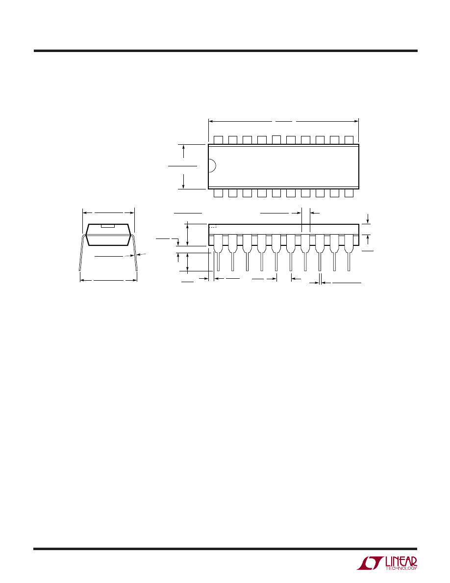
26
LTC1090
1090fc
N Package
20-Lead PDIP (Narrow .300 Inch)
(Reference LTC DWG # 05-08-1510)
N20 1098
0.020
(0.508)
MIN
0.125
(3.175)
MIN
0.130
±
0.005
(3.302
±
0.127)
0.065
(1.651)
TYP
0.045 – 0.065
(1.143 – 1.651)
0.018
±
0.003
(0.457
±
0.076)
0.005
(0.127)
MIN
0.100
(2.54)
BSC
0.255
±
0.015*
(6.477
±
0.381)
1.040*
(26.416)
MAX
1
2
3
4
5
6
7
8
9
10
19
11
12
13
14
16
15
17
18
20
0.009 – 0.015
(0.229 – 0.381)
0.300 – 0.325
(7.620 – 8.255)
0.325
+0.035
–0.015
+0.889
–0.381
8.255
(
)
*THESE DIMENSIONS DO NOT INCLUDE MOLD FLASH OR PROTRUSIONS.
MOLD FLASH OR PROTRUSIONS SHALL NOT EXCEED 0.010 INCH (0.254mm)
U
PACKAGE DESCRIPTIO
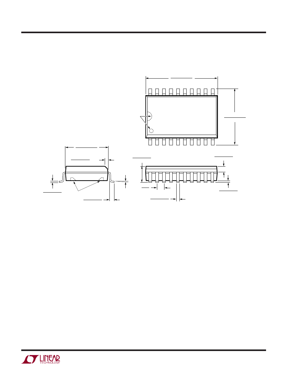
27
LTC1090
1090fc
Information furnished by Linear Technology Corporation is believed to be accurate and reliable.
However, no responsibility is assumed for its use. Linear Technology Corporation makes no represen-
tation that the interconnection of its circuits as described herein will not infringe on existing patent rights.
U
PACKAGE DESCRIPTIO
S20 (WIDE) 1098
NOTE 1
0.496 – 0.512*
(12.598 – 13.005)
20
19
18
17
16
15
14
13
1
2
3
4
5
6
7
8
0.394 – 0.419
(10.007 – 10.643)
9
10
11
12
0.037 – 0.045
(0.940 – 1.143)
0.004 – 0.012
(0.102 – 0.305)
0.093 – 0.104
(2.362 – 2.642)
0.050
(1.270)
BSC
0.014 – 0.019
(0.356 – 0.482)
TYP
0
°
– 8
°
TYP
NOTE 1
0.009 – 0.013
(0.229 – 0.330)
0.016 – 0.050
(0.406 – 1.270)
0.291 – 0.299**
(7.391 – 7.595)
×
45
°
0.010 – 0.029
(0.254 – 0.737)
NOTE:
1. PIN 1 IDENT, NOTCH ON TOP AND CAVITIES ON THE BOTTOM OF PACKAGES ARE THE MANUFACTURING OPTIONS.
THE PART MAY BE SUPPLIED WITH OR WITHOUT ANY OF THE OPTIONS
DIMENSION DOES NOT INCLUDE MOLD FLASH. MOLD FLASH SHALL NOT EXCEED 0.006" (0.152mm) PER SIDE
DIMENSION DOES NOT INCLUDE INTERLEAD FLASH. INTERLEAD FLASH SHALL NOT EXCEED 0.010" (0.254mm) PER SIDE
*
**
SW Package
20-Lead Plastic Small Outline (Wide .300 Inch)
(Reference LTC DWG # 05-08-1620)
28
LTC1090
1090fc
Linear Technology Corporation
1630 McCarthy Blvd., Milpitas, CA 95035-7417
(408) 432-1900
●
FAX: (408) 434-0507
●
www.linear.com
LW/TP 0902 1K REV C • PRINTED IN USA
LINEAR TECHNOLOGY CORPORATION 1990
PART NUMBER
DESCRIPTION
COMMENTS
LTC1290
8-Channel Configurable, 5V, 12-Bit ADC
Pin-Compatible with LTC1090
LTC1391
Serial-Controlled 8-to-1 Analog Multiplexer
Low R
ON
, Low Power, 16-Pin SO and SSOP Package
LTC1594L/LTC1598L
4-/8-Channel, 3V Micropower 12-Bit ADC
Low Power, Small Size
LTC1850/LTC1851
10-Bit/12-Bit, 8-Channel, 1.25Msps ADCs
5V, Programmable MUX and Sequencer
LTC1852/LTC1853
10-Bit/12-Bit, 8-Channel, 400ksps ADCs
3V or 5V, Programmable MUX and Sequencer
LTC2404/LTC2408
24-Bit, 4-/8-Channel, No Latency ∆Σ
TM
ADC
4ppm INL, 10ppm Total Unadjusted Error, 200µA
LTC2424/LTC2428
20-Bit, 4-/8-Channel, No Latency ∆Σ ADC
1.2ppm Noise, 8ppm INL, Pin Compatible with LTC2404/LTC2408
RELATED PARTS
No Latency ∆Σ is a trademark of Linear Technology Corporation.
Wyszukiwarka
Podobne podstrony:
LTC109x (Linear Technology)
Linear Technology Top Markings Nieznany
Linear Technology Top Markings Nieznany
LTC1290 (Linear Technology)
PORÓWNYWANIE TECHNOLOGII
19 Mikroinżynieria przestrzenna procesy technologiczne,
Technologia informacji i komunikacji w nowoczesnej szkole
Technologia spawania stali wysokostopowych 97 2003
SII 17 Technologie mobilne
W WO 2013 technologia
TECHNOLOGIA PŁYNNYCH POSTACI LEKU Zawiesiny
technologia prefabrykowana
Technology & Iventions
Technologia Maszyn CAD CAM
1 Infrastruktura, technika i technologia procesów logistyczid 8534 ppt
więcej podobnych podstron