1
LTC1290
1290fe
, LTC and LT are registered trademarks of Linear Technology Corporation.
LTCMOS is a trademark of Linear Technology Corporation. All other trademarks
are the property of their respective owners. Protected by U.S. Patents, including 5287525.
DESCRIPTIO
U
KEY SPECIFICATIO S
U
FEATURES
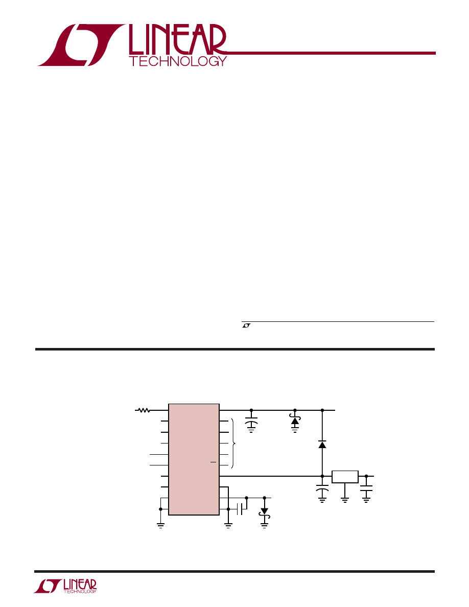
Single Chip 12-Bit Data
Acquisition System
12-Bit 8-Channel Sampling Data Acquisition System
CH0
CH1
CH2
CH3
CH4
CH5
CH6
CH7
COM
DGND
V
CC
ACLK
SCLK
D
IN
D
OUT
CS
REF
+
REF
–
V
–
AGND
LTC1290
DIFFERENTIAL INPUT (+)
±5V COMMON MODE RANGE (–)
•
•
•
•
•
•
1k
SINGLE-ENDED INPUT
0V TO 5V OR
±5V
±15V OVERVOLTAGE RANGE*
TO AND FROM
MICROPROCESSOR
0.1
µF
1N5817
–5V
22
µF
TANTALUM
1N5817
1N4148
4.7
µF
TANTALUM
1
µF
LT
®
1027
5V
8V TO 40V
* FOR OVERVOLTAGE PROTECTION ON ONLY ONE CHANNEL LIMIT THE INPUT CURRENT TO 15mA. FOR OVERVOLTAGE PROTECTION
ON MORE THAN ONE CHANNEL LIMIT THE INPUT CURRENT TO 7mA PER CHANNEL AND 28mA FOR ALL CHANNELS. (SEE SECTION ON
OVERVOLTAGE PROTECTION IN THE APPLICATIONS INFORMATION SECTION.) CONVERSION RESULTS ARE NOT VALID WHEN THE SELECTED
OR ANY OTHER CHANNEL IS OVERVOLTAGED (V
IN
< V
–
OR V
IN
> V
CC
).
1290 • TA01
+
+
The LTC
®
1290 is a data acquisition component which
contains a serial I/O successive approximation A/D con-
verter. It uses LTCMOS
TM
switched capacitor technology
to perform either 12-bit unipolar or 11-bit plus sign bipolar
A/D conversions. The 8-channel input multiplexer can be
configured for either single-ended or differential inputs (or
combinations thereof). An on-chip sample-and-hold is
included for all single-ended input channels. When the
LTC1290 is idle it can be powered down with a serial word
in applications where low power consumption is desired.
The serial I/O is designed to be compatible with industry
standard full duplex serial interfaces. It allows either MSB-
or LSB-first data and automatically provides 2's comple-
ment output coding in the bipolar mode. The output data
word can be programmed for a length of 8, 12 or 16 bits.
This allows easy interface to shift registers and a variety of
processors.
■
Software Programmable Features
– Unipolar/Bipolar Conversion
– Four Differential/Eight Single-Ended Inputs
– MSB- or LSB-First Data Sequence
– Variable Data Word Length
– Power Shutdown
■
Built-In Sample-and-Hold
■
Single Supply 5V or
±5V Operation
■
Direct Four-Wire Interface to Most MPU Serial Ports
and All MPU Parallel Ports
■
50kHz Maximum Throughput Rate
■
Available in 20-Lead PDIP and SO Wide Packages
■
Resolution: 12 Bits
■
Fast Conversion Time: 13
µs Max Over Temp
■
Low Supply Current: 6.0mA
TYPICAL APPLICATIO
U
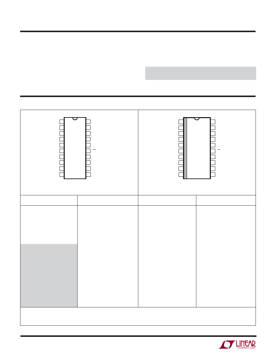
2
LTC1290
1290fe
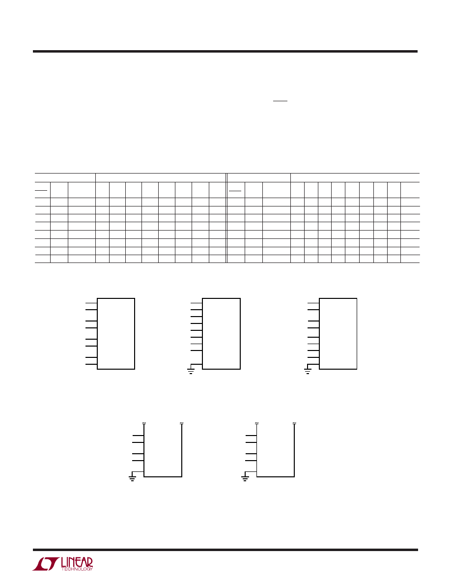
1
2
3
4
5
6
7
8
9
10
TOP VIEW
SW PACKAGE
20-LEAD PLASTIC SO WIDE
20
19
18
17
16
15
14
13
12
11
CH0
CH1
CH2
CH3
CH4
CH5
CH6
CH7
COM
DGND
V
CC
ACLK
SCLK
D
IN
D
OUT
CS
REF
+
REF
–
V
–
AGND
1
2
3
4
5
6
7
8
9
10
TOP VIEW
N PACKAGE
20-LEAD PDIP
20
19
18
17
16
15
14
13
12
11
CH0
CH1
CH2
CH3
CH4
CH5
CH6
CH7
COM
DGND
V
CC
ACLK
SCLK
D
IN
D
OUT
CS
REF
+
REF
–
V
–
AGND
A
U
G
W
A
W
U
W
A
R
BSOLUTE
XI
TI
S
Supply Voltage (V
CC
) to GND or V
–
........................ 12V
Negative Supply Voltage (V
–
) .................... – 6V to GND
Voltage
Analog/Reference Inputs ......... (V
–
) – 0.3V to V
CC
+ 0.3V
Digital Inputs ........................................ – 0.3V to 12V
Digital Outputs ........................... – 0.3V to V
CC
+ 0.3V
Power Dissipation ............................................. 500mW
(Notes 1, 2)
Operating Temperature Range
LTC1290BC, LTC1290CC, LTC1290DC .... 0
°C to 70°C
LTC1290BI, LTC1290CI, LTC1290DI .... – 40
°C to 85°C
LTC1290BM, LTC1290CM,
LTC1290DM (OBSOLETE) ............ – 55
°C to 125°C
Storage Temperature Range ................ – 65
°C to 150°C
Lead Temperature (Soldering, 10 sec.)................ 300
°C
W
U
U
PACKAGE/ORDER I FOR ATIO
LTC1290BCSW
LTC1290CCSW
LTC1290DCSW
LTC1290BISW
LTC1290CISW
LTC1290DISW
T
JMAX
= 110
°C, θ
JA
= 130
°C/W (SW)
ORDER PART NUMBER
LTC1290BIN
LTC1290CIN
LTC1290DIN
LTC1290BCN
LTC1290CCN
LTC1290DCN
T
JMAX
= 110
°C, θ
JA
= 100
°C/W (N)
LTC1290BMJ
LTC1290CMJ
LTC1290DMJ
LTC1290BIJ
LTC1290CIJ
LTC1290DIJ
OBSOLETE PACKAGE
Consider N Package for Alternate Source
J PACKAGE
20-LEAD CERAMIC DIP
T
JMAX
= 150
°C, q
JA
= 80
°C/W (J)
*The temperature grade is identified by a label on the shipping container. Consult LTC Marketing for parts specified with wider operating temperature ranges.
N PART MARKING
ORDER PART NUMBER
SW PART MARKING
Order Options
Tape and Reel: Add #TR
Lead Free: Add #PBF Lead Free Tape and Reel: Add #TRPBF
Lead Free Part Marking:
3
LTC1290
1290fe
LTC1290B
LTC1290C
LTC1290D
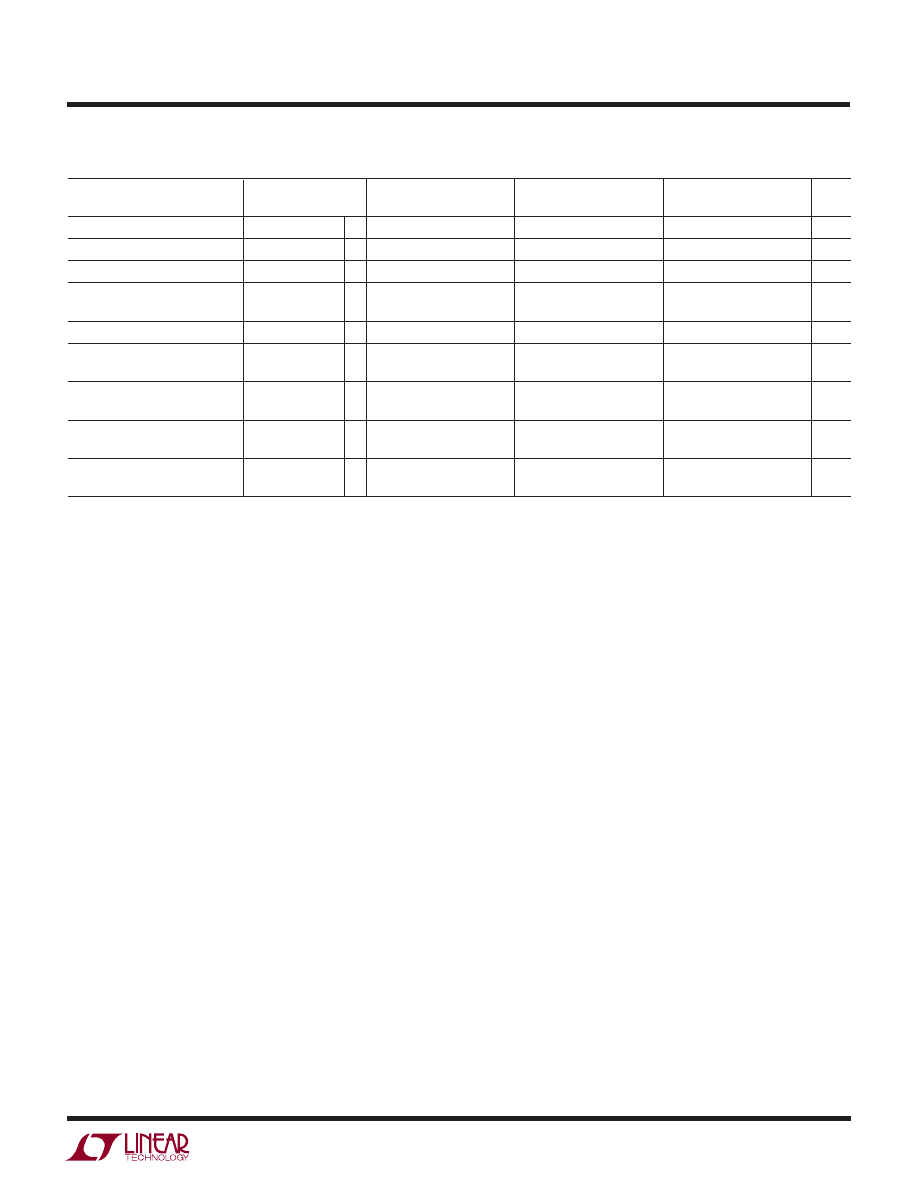
PARAMETER
CONDITIONS
MIN
TYP
MAX
MIN
TYP
MAX
MIN
TYP
MAX
UNITS
Offset Error
(Note 4)
●
±1.5
±1.5
±1.5
LSB
Linearity Error (INL)
(Notes 4, 5)
●
±0.5
±0.5
±0.75
LSB
Gain Error
(Note 4)
●
±0.5
±1.0
±4.0
LSB
Minimum Resolution for Which
●
12
12
12
Bits
No Missing Codes are Guaranteed
Analog and REF Input Range
(Note 7)
(V
–
) – 0.05V to V
CC
+ 0.05V (V
–
) – 0.05V to V
CC
+ 0.05V (V
–
) – 0.05V to V
CC
+ 0.05V
V
On Channel Leakage Current
On Channel = 5V
●
±1
±1
±1
µA
(Note 8)
Off Channel = 0V
On Channel = 0V
●
±1
±1
±1
µA
Off Channel = 5V
Off Channel Leakage Current
On Channel = 5V
●
±1
±1
±1
µA
(Note 8)
Off Channel = 0V
On Channel = 0V
●
±1
±1
±1
µA
Off Channel = 5V
CO VERTER A D ULTIPLEXER CHARACTERISTICS
U
U W
The
●
denotes the specifications
which apply over the full operating temperature range, otherwise specifications are at T
A
= 25
°C. (Note 3)
4
LTC1290
1290fe
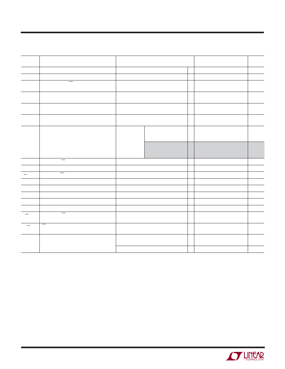
AC CHARACTERISTICS
The
●
denotes the specifications which apply over the full operating temperature range,
otherwise specifications are at T
A
= 25
°C. (Note 3)
LTC1290B/LTC1290C/LTC1290D
SYMBOL
PARAMETER
CONDITIONS
MIN
TYP
MAX
UNITS
f
SCLK
Shift Clock Frequency
V
CC
= 5V (Note 6)
0
2.0
MHz
f
ACLK
A/D Clock Frequency
V
CC
= 5V (Note 6)
(Note 10)
4.0
MHz
t
ACC
Delay Time from CS
↓ to D
OUT
Data Valid
(Note 9)
2
ACLK
Cycles
t
SMPL
Analog Input Sample Time
See Operating Sequence
7
SCLK
Cycles
t
CONV
Conversion Time
See Operating Sequence
52
ACLK
Cycles
t
CYC
Total Cycle Time
See Operating Sequence (Note 6)
12 SCLK +
Cycles
56 ACLK
t
dDO
Delay Time, SCLK
↓ to D
OUT
Data Valid
See Test Circuits LTC1290BC, LTC1290CC
●
130
220
ns
LTC1290DC, LTC1290BI
LTC1290CI, LTC1290DI
LTC1290BM, LTC1290CM
●
180
270
ns
LTC1290DM
(OBSOLETE)
t
dis
Delay Time, CS
↑ to D
OUT
Hi-Z
See Test Circuits
●
70
100
ns
t
en
Delay Time, 2nd ACLK
↓ to D
OUT
Enabled
See Test Circuits
●
130
200
ns
t
hCS
Hold Time, CS After Last SCLK
↓
V
CC
= 5V (Note 6)
0
ns
t
hDI
Hold Time, D
IN
After SCLK
↑
V
CC
= 5V (Note 6)
50
ns
t
hDO
Time Output Data Remains Valid After SCLK
↓
50
ns
t
f
D
OUT
Fall Time
See Test Circuits
●
65
130
ns
t
r
D
OUT
Rise Time
See Test Circuits
●
25
50
ns
t
suDI
Setup Time, D
IN
Stable Before SCLK
↑
V
CC
= 5V (Note 6)
50
ns
t
suCS
Setup Time, CS
↓ Before Clocking in
(Notes 6, 9)
2 ACLK Cycles
First Address Bit
+ 100ns
t
WHCS
CS High Time During Conversion
V
CC
= 5V (Note 6)
52
ACLK
Cycles
C
IN
Input Capacitance
Analog Inputs On Channel
100
pF
Analog Inputs Off Channel
5
pF
Digital Inputs
5
pF
5
LTC1290
1290fe
LTC1290B/LTC1290C/LTC1290D
SYMBOL
PARAMETER
CONDITIONS
MIN
TYP
MAX
UNITS
V
IH
High Level Input Voltage
V
CC
= 5.25V
●
2.0
V
V
IL
Low Level Input Voltage
V
CC
= 4.75V
●
0.8
V
I
IH
High Level Input Current
V
IN
= V
CC
●
2.5
µA
I
IL
Low Level Input Current
V
IN
= 0V
●
– 2.5
µA
V
OH
High Level Output Voltage
V
CC
= 4.75V
I
O
= 10
µA
4.7
V
I
O
= 360
µA
●
2.4
4.0
V
V
OL
Low Level Output Voltage
V
CC
= 4.75V
I
O
= 1.6mA
●
0.4
V
I
OZ
High-Z Output Leakage
V
OUT
= V
CC
, CS High
●
3
µA
V
OUT
= 0V, CS High
●
– 3
µA
I
SOURCE
Output Source Current
V
OUT
= 0V
–20
mA
I
SINK
Output Sink Current
V
OUT
= V
CC
20
mA
I
CC
Positive Supply Current
CS High
●
6
12
mA
CS High
LTC1290BC, LTC1290CC
●
5
10
µA
Power Shutdown LTC1290DC, LTC1290BI
ACLK Off
LTC1290CI, LTC1290DI
LTC1290BM, LTC1290CM
●
5
15
µA
LTC1290DM
(OBSOLETE)
I
REF
Reference Current
V
REF
= 5V
●
10
50
µA
I
–
Negative Supply Current
CS High
●
1
50
µA
V
CC
levels (4.5V), as high level reference or analog inputs (5V) can cause
this input diode to conduct, especially at elevated temperatures and cause
errors for inputs near full scale. This spec allows 50mV forward bias of
either diode. This means that as long as the reference or analog input does
not exceed the supply voltage by more than 50mV, the output code will be
correct. To achieve an absolute 0V to 5V input voltage range will therefore
require a minimum supply voltage of 4.950V over initial tolerance,
temperature variations and loading.
Note 8: Channel leakage current is measured after the channel selection.
Note 9: To minimize errors caused by noise at the chip select input, the
internal circuitry waits for two ACLK falling edge after a chip select falling
edge is detected before responding to control input signals. Therefore, no
attempt should be made to clock an address in or data out until the
minimum chip select setup time has elapsed.
Note 10: Increased leakage currents at elevated temperatures cause the
S/H to droop, therefore it's recommended that f
ACLK
≥ 125kHz at 85°C and
f
ACLK
≥ 15kHz at 25°C.
Note 1: Absolute Maximum Ratings are those values beyond which the life
of a device may be impaired.
Note 2: All voltage values are with respect to ground with DGND, AGND
and REF
–
wired together (unless otherwise noted).
Note 3: V
CC
= 5V, V
REF +
= 5V, V
REF –
= 0V, V
–
= 0V for unipolar mode and
– 5V for bipolar mode, ACLK = 4.0MHz unless otherwise specified.
Note 4: These specs apply for both unipolar and bipolar modes. In bipolar
mode, one LSB is equal to the bipolar input span (2V
REF
) divided by 4096.
For example, when V
REF
= 5V, 1LSB (bipolar) = 2(5V)/4096 = 2.44mV.
Note 5: Integral nonlinearity is defined as the deviation of a code from a
straight line passing through the actual endpoints of the transfer curve.
The deviation is measured from the center of the quantization band.
Note 6: Recommended operating conditions.
Note 7: Two on-chip diodes are tied to each reference and analog input
which will conduct for reference or analog input voltages one diode drop
below V
–
or one diode drop above V
CC
. Be careful during testing at low
ELECTRICAL C
C
HARA TER STICS
DIGITAL A D
U
I
DC
The
●
denotes the specifications which
apply over the full operating temperature range, otherwise specifications are at T
A
= 25
°C. (Note 3)
6
LTC1290
1290fe
C
C
HARA TERISTICS
U
W
A
TYPICAL PERFOR
CE
Change in Offset vs Temperature
Change in Linearity vs Reference
Voltage
REFERENCE VOLTAGE, V
REF
(V)
0
LINEARITY ERROR (LSB = • V
REF
)
1.25
1.00
0.75
0.50
0.25
0
4
1290 • TPC04
1
2
3
5
1
4096
V
CC
= 5V
Change in Gain vs Reference
Voltage
REFERENCE VOLTAGE, V
REF
(V)
1
CHANGE IN GAIN ERROR (LSB = • V
REF
)
–0.2
–0.1
0
5
1290 • TPC05
–0.3
–0.4
–0.5
2
3
4
1
4096
V
CC
= 5V
AMBIENT TEMPERATURE, T
A
(
°C)
–50
MAGNITUDE OF OFFSET CHANGE
⏐∆
OFFSET
⏐
(LSB)
0.5
0.4
0.3
0.2
0.1
0
–10
30
50
130
1290 • TPC06
–30
10
70
90 110
ACLK = 4MHz
V
CC
= 5V
V
REF
= 5V
Change in Gain Error vs
Temperature
AMBIENT TEMPERATURE, T
A
(
°C)
–50
MAGNITUDE OF GAIN CHANGE
⏐∆
GAIN
⏐
(LSB)
0.5
0.4
0.3
0.2
0.1
0
–10
30
50
130
1290 • TPC08
–30
10
70
90 110
ACLK = 4MHz
V
CC
= 5V
V
REF
= 5V
Change in Linearity Error vs
Temperature
AMBIENT TEMPERATURE, T
A
(
°C)
–50
0
MAGNITUDE OF LINEARITY CHANGE
⏐∆
LINEARITY
⏐
(LSB)
0.1
0.3
0.4
0.5
–10
30
50
130
1290 • TPC07
0.2
–30
10
70
90 110
0.6
ACLK = 4MHz
V
CC
= 5V
V
REF
= 5V
Maximum ACLK Frequency vs
Source Resistance
R
SOURCE
(
Ω)
100
0
MAXIMUM ACLK FREQUENCY* (MHz)
4
5
1k
10 k
100k
1290 • TPC09
3
2
1
V
CC
= 5V
V
REF
= 5V
T
A
= 25
°C
+
–
INPUT
INPUT
V
IN
R
SOURCE–
* MAXIMUM ACLK FREQUENCY REPRESENTS THE
ACLK FREQUENCY AT WHICH A 0.1LSB SHIFT IN
THE ERROR AT ANY CODE TRANSITION FROM ITS
4MHz VALUE IS FIRST DETECTED.
Supply Current vs Temperature
Supply Current vs Supply Voltage
Unadjusted Offset Voltage vs
Reference Voltage
SUPPLY VOLTAGE, V
CC
(V)
4
6
8
10
SUPPLY CURRENT, I
CC
(mA)
1290 • TPC01
26
22
18
14
10
6
2
ACLK = 4MHz
T
A
= 25
°C
AMBIENT TEMPERATURE, T
A
(
°C)
–50
SUPPLY CURRENT, I
CC
(mA)
30
10
9
8
7
6
5
4
3
LT1290 • TPC02
–10
70
–30
50
10
90 110 130
ACLK = 4MHz
V
CC
= 5V
REFERENCE VOLTAGE, V
REF
(V)
1
OFFSET ERROR (LSB = • V
REF
)
5
1290 • TPC03
2
3
4
0.9
0.8
0.7
0.6
0.5
0.4
0.3
0.2
0.1
1
4096
V
OS
= 0.25mV
V
OS
= 0.125mV
V
CC
= 5V
7
LTC1290
1290fe
Sample-and-Hold Acquisition
Time vs Source Resistance
R
SOURCE
+ (
Ω)
100
1
S & H AQUISITION TIME TO 0.02% (
µ
s)
10
100
1k
10k
LTC1290 • TPC11
+
–
V
IN
R
SOURCE
+
V
REF
= 5V
V
CC
= 5V
T
A
= 25
°C
0V TO 5V INPUT STEP
ACLK FREQUENCY (MHz)
0
SUPPLY CURRENT, I
CC
(
µ
A)
1.00
2.00
3.00
4.00
1290 • TPC13
200
180
160
140
120
100
80
60
40
20
V
CC
= 5V
CMOS LEVELS
Supply Current (Power Shutdown)
vs ACLK
Supply Current (Power Shutdown)
vs Temperature
AMBIENT TEMPERATURE, T
A
(
°C)
–50
SUPPLY CURRENT, I
CC
(
µ
A)
10
9
8
7
6
5
4
3
2
1
0
–10
30
50
130
1290 • TPC12
–30
10
70
90 110
ACLK OFF DURING
POWER SHUTDOWN
Input Channel Leakage Current
vs Temperature
AMBIENT TEMPERATURE, T
A
(
°C)
–50
0
INPUT CHANNEL LEAKAGE CURRENT (nA)
100
300
400
500
1000
700
–10
30
50
130
1290 • TPC14
200
800
900
600
–30
10
70
90 110
ON CHANNEL
OFF CHANNEL
GUARANTEED
Noise Error vs Reference Voltage
REFERENCE VOLTAGE, V
REF
(V)
0
0
PEAK-TO-PEAK NOISE ERROR (LSBs) 0.25
0.75
1.00
1.25
2
4
5
2.25
1290 • TPC15
0.50
1
3
1.50
1.75
2.00
LTC1290 NOISE 200
µV
P-P
CH0 to CH7 (Pin 1 to Pin 8): Analog Inputs. The analog
inputs must be free of noise with respect to AGND.
COM (Pin 9): Common. The common pin defines the zero
reference point for all single-ended inputs. It must be free
of noise and is usually tied to the analog ground plane.
DGND (Pin 10): Digital Ground. This is the ground for the
internal logic. Tie to the ground plane.
AGND (Pin 11): Analog Ground. AGND should be tied
directly to the analog ground plane.
V
–
(Pin 12): Negative Supply. Tie V
–
to most negative
potential in the circuit. (Ground in single supply applica-
tions.)
REF
–
, REF
+
(Pins 13, 14): Reference Inputs. The refer-
ence inputs must be kept free of noise with respect to
AGND.
CS (Pin 15): Chip Select Input. A logic low on this input
enables data transfer.
D
OUT
(Pin 16): Digital Data Output. The A/D conversion
result is shifted out of this output.
Maximum Filter Resistor vs
Cycle Time
CYCLE TIME, t
CYC
(
µs)
MAXIMUM R
FILTER
** (
Ω
)
10
100
1k
10k
10
1000
10000
1290 • TPC10
1.0
100
+
–
V
IN
C
FILTER
≥ 1µF
R
FILTER
** MAXIMUM R
FILTER
REPRESENTS THE FILTER RESISTOR
VALUE AT WHICH A 0.1LSB CHANGE IN FULL-SCALE
ERROR FROM ITS VALUE AT R
FILTER
= 0 IS FIRST DETECTED.
TYPICAL PERFOR A CE CHARACTERISTICS
U
W
U
U
U
PI FU CTIO S
8
LTC1290
1290fe
PI FU CTIO S
U
U
U
D
IN
(Pin 17): Digital Data Input. The A/D configuration
word is shifted into this input after CS is recognized.
SCLK (Pin 18): Shift Clock. This clock synchronizes the
serial data transfer.
ACLK (Pin 19): A/D Conversion Clock. This clock controls
the A/D conversion process.
V
CC
(Pin 20): Positive Supply. This supply must be kept
free of noise and ripple by bypassing directly to the analog
ground plane.
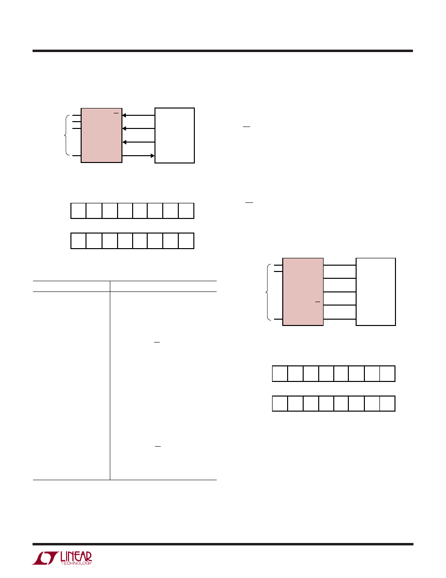
BLOCK DIAGRAM
INPUT
SHIFT
REGISTER
SAMPLE-
AND-
HOLD
12-BIT
CAPACITIVE
DAC
V
CC
20
ANALOG
INPUT MUX
1
2
3
4
5
6
7
8
9
CH0
CH1
CH2
CH3
CH4
CH5
CH6
CH7
COM
D
OUT
16
SCLK
18
CONTROL
AND
TIMING
15
CS
LTC1290 • BD
17
REF
+
14
DGND
10
AGND
11
V
–
12
REF
–
13
COMP
OUTPUT
SHIFT
REGISTER
D
IN
19
ACLK
12-BIT
SAR
TEST CIRCUITS
5V
A
A
I
OFF
I
ON
POLARITY
OFF
CHANNELS
ON CHANNEL
LTC1290 • TC01
•
•
•
•
On and Off Channel Leakage Current
Load Circuit for t
dis
and t
en
D
OUT
3k
100pF
TEST POINT
5V WAVEFORM 2
WAVEFORM 1
LTC1290 • TC02
9
LTC1290
1290fe
TEST CIRCUITS
Voltage Waveforms for D
OUT
Delay Time, t
dDO
Load Circuit for t
dDO
, t
r
and t
f
Voltage Waveform for D
OUT
Rise and Fall Times, t
r
, t
f
Voltage Waveforms for t
en
and t
dis
D
OUT
1.4V
3k
100pF
TEST POINT
1290 • TC05
SCLK
D
OUT
0.8V
t
dDO
0.4V
2.4V
LTC1290 • TC03
D
OUT
0.4V
2.4V
t
r
t
f
LTC1290 • TC04
D
OUT
WAVEFORM 1
(SEE NOTE 1)
t
dis
90%
10%
D
OUT
WAVEFORM 2
(SEE NOTE 2)
CS
NOTE 1: WAVEFORM 1 IS FOR AN OUTPUT WITH INTERNAL CONDITIONS SUCH THAT THE OUTPUT IS HIGH UNLESS DISABLED BY THE OUTPUT CONTROL.
NOTE 2: WAVEFORM 2 IS FOR AN OUTPUT WITH INTERNAL CONDITIONS SUCH THAT THE OUTPUT IS LOW UNLESS DISABLED BY THE OUTPUT CONTROL.
LTC1290 • TC06
t
en
2.4V
0.8V
ACLK
1
2
2.0V
10
LTC1290
1290fe
U
S
A
O
PPLICATI
W
U
U
I FOR ATIO
previous conversion is output on the D
OUT
line. At the end
of the data exchange the requested conversion begins and
CS should be brought high. After t
CONV
, the conversion is
complete and the results will be available on the next data
transfer cycle. As shown below, the result of a conversion
is delayed by one CS cycle from the input word requesting it.
The LTC1290 is a data acquisition component which
contains the following functional blocks:
1. 12-bit successive approximation capacitive A/D
converter
2. Analog multiplexer (MUX)
3. Sample-and-hold (S/H)
4. Synchronous, full duplex serial interface
5. Control and timing logic
DIGITAL CONSIDERATIONS
Serial Interface
The LTC1290 communicates with microprocessors and
other external circuitry via a synchronous, full duplex,
four-wire serial interface (see Operating Sequence). The
shift clock (SCLK) synchronizes the data transfer with
each bit being transmitted on the falling SCLK edge and
captured on the rising SCLK edge in both transmitting and
receiving systems. The data is transmitted and received
simultaneously (full duplex).
Data transfer is initiated by a falling chip select (CS) signal.
After the falling CS is recognized, an 8-bit input word is
shifted into the D
IN
input which configures the LTC1290
for the next conversion. Simultaneously, the result of the
SGL/
DIFF
SELECT
1
SELECT
0
UNI
MSBF
WL1
MUX ADDRESS
MSB-FIRST/
LSB-FIRST
UNIPOLAR/
BIPOLAR
WORD
LENGTH
LTC1290 • AI02
ODD/
SIGN
WL0
D
IN
D
OUT
D
OUT
WORD 0
D
IN
WORD 1
DATA
TRANSFER
D
OUT
WORD 2
D
IN
WORD 3
D
OUT
WORD 1
D
IN
WORD 2
DATA
TRANSFER
t
CONV
A/D
CONVERSION
t
CONV
A/D
CONVERSION
LTC1290 • AI01
Input Data Word
The LTC1290 8-bit data word is clocked into the D
IN
input
on the first eight rising SCLK edges after chip select is
recognized. Further inputs on the D
IN
pin are then ignored
until the next CS cycle. The eight bits of the input word are
defined as follows:
1
2
3
4
5
6
7
8
9
10
11
12
tCONV
tCYC
SHIFT CONFIGURATION
WORD IN
tSMPL
SHIFT A/D RESULT OUT AND
NEW CONFIGURATION WORD IN
B11 B10 B9
B8
B7
B6 B5
B4
B3
B2
B1
B0
(SB)
LTC1290 • AI03
SCLK
DIN
DOUT
CS
DON’T CARE
DON’T CARE
Operating Sequence
(Example: Differential Inputs (CH3-CH2), Bipolar, MSB-First and 12-Bit Word Length)
11
LTC1290
1290fe
U
S
A
O
PPLICATI
W
U
U
I FOR ATIO
MUX Address
The first four bits of the input word assign the MUX
configuration for the requested conversion. For a given
channel selection, the converter will measure the voltage
between the two channels indicated by the + and – signs
in the selected row of Table 1. Note that in differential
MUX ADDRESS
DIFFERENTIAL CHANNEL SELECTION
Table 1. Multiplexer Channel Selection
MUX ADDRESS
SGL/
DIFF
SELECT
1 0
ODD
SIGN
1
0
0
0
+
–
1
0
0
1
+
–
1
0
1
0
+
–
1
0
1
1
+
–
1
1
0
0
+
–
1
1
0
1
+
–
1
1
1
0
+
–
1
1
1
1
+
–
SGL/
DIFF
ODD
SIGN
SELECT
1 0
0
0
0
0
+
–
0
0
0
1
+
–
0
0
1
0
+
–
0
0
1
1
+
–
0
1
0
0
–
+
0
1
0
1
–
+
0
1
1
0
–
+
0
1
1
1
–
+
0
1
2
3
4
5
6
7
0 1 2 3 4 5 6 7 COM
SINGLE-ENDED CHANNEL SELECTION
mode (SGL/DIFF = 0) measurements are limited to four
adjacent input pairs with either polarity. In single-ended
mode, all input channels are measured with respect to
COM.
Figure 1. Examples of Multiplexer Options on the LTC1290
0
1
2
3
4
5
6
7
CHANNEL
COM (
–
)
8 Single-Ended
+
+
+
+
+
+
+
0,1
CHANNEL
4 Differential
2,3
4,5
6,7
+
(
–
)
+
+
(
–
)
+
(
–
)
+
(
–
)
–
(
+
)
–
(
+
)
–
(
+
)
–
(
+
)
4
5
6
7
CHANNEL
COM (
–
)
Combinations of Differential and Single-Ended
+
+
+
+
+
+
0,1
2,3
–
–
COM (UNUSED)
Changing the MUX Assignment “On the Fly”
COM (
–
)
4,5
6,7
5,4
1ST CONVERSION
2ND CONVERSION
+
–
+
–
+
–
+
+
7
6
{
{
{
{
{
{
{
{
{
{
LTC1290 • F01
12
LTC1290
1290fe
U
S
A
O
PPLICATI
W
U
U
I FOR ATIO
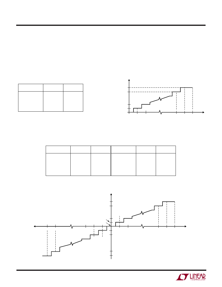
Unipolar/Bipolar (UNI)
The fifth input bit (UNI) determines whether the conver-
sion will be unipolar or bipolar. When UNI is a logical one,
a unipolar conversion will be performed on the selected
Unipolar Transfer Curve (UNI = 1)
input voltage. When UNI is a logical zero, a bipolar conver-
sion will result. The input span and code assignment for
each conversion type are shown in the figures below.
Unipolar Output Code (UNI = 1)
Bipolar Transfer Curve (UNI = 0)
Bipolar Output Code (UNI = 0)
0V
1LSB
V
REF
– 2LSB
V
REF
– 1LSB
V
REF
V
IN
0 0 0 0 0 0 0 0 0 0 0 1
0 0 0 0 0 0 0 0 0 0 0 0
1 1 1 1 1 1 1 1 1 1 1 1
1 1 1 1 1 1 1 1 1 1 1 0
•
•
•
LTC1290 AI04b
OUTPUT CODE
1 1 1 1 1 1 1 1 1 1 1 1
1 1 1 1 1 1 1 1 1 1 1 0
•
•
•
0 0 0 0 0 0 0 0 0 0 0 1
0 0 0 0 0 0 0 0 0 0 0 0
INPUT VOLTAGE
V
REF
– 1LSB
V
REF
– 2LSB
•
•
•
1LSB
0V
INPUT VOLTAGE
(V
REF
= 5V)
4.9988V
4.9976V
•
•
•
0.0012V
0V
LTC1290 • AI04a
OUTPUT CODE
1 1 1 1 1 1 1 1 1 1 1 1
1 1 1 1 1 1 1 1 1 1 1 0
•
•
•
1 0 0 0 0 0 0 0 0 0 0 1
1 0 0 0 0 0 0 0 0 0 0 0
INPUT VOLTAGE
–1LSB
–2LSB
•
•
•
–(V
REF
) + 1LSB
– (V
REF
)
INPUT VOLTAGE
(V
REF
= 5V)
–0.0024V
–0.0048V
•
•
•
–4.9976V
–5.0000V
OUTPUT CODE
0 1 1 1 1 1 1 1 1 1 1 1
0 1 1 1 1 1 1 1 1 1 1 0
•
•
•
0 0 0 0 0 0 0 0 0 0 0 1
0 0 0 0 0 0 0 0 0 0 0 0
INPUT VOLTAGE
V
REF
– 1LSB
V
REF
– 2LSB
•
•
•
1LSB
0V
INPUT VOLTAGE
(V
REF
= 5V)
4.9976V
4.9851V
•
•
•
0.0024V
0V
LTC1290 AI05a
1LSB
V
REF
– 2LSB
V
REF
– 1LSB
V
REF
V
IN
1 1 1 1 1 1 1 1 1 1 1 1
0 0 0 0 0 0 0 0 0 0 0 1
0 0 0 0 0 0 0 0 0 0 0 0
0 1 1 1 1 1 1 1 1 1 1 0
0 1 1 1 1 1 1 1 1 1 1 1
1 1 1 1 1 1 1 1 1 1 1 0
•
•
•
1 0 0 0 0 0 0 0 0 0 0 1
1 0 0 0 0 0 0 0 0 0 0 0
–1LSB
–2LSB
–V
REF
–V
REF
+ 1LSB
•
•
•
LTC1290 AI05b
13
LTC1290
1290fe
U
S
A
O
PPLICATI
W
U
U
I FOR ATIO
MSB-First/LSB-First Format (MSBF)
The output data of the LTC1290 is programmed for MSB-
first or LSB-first sequence using the MSBF bit. For MSB
first output data the input word clocked to the LTC1290
should always contain a logical one in the sixth bit location
(MSBF bit). Likewise for LSB-first output data the input
word clocked to the LTC1290 should always contain a zero
in the MSBF bit location. The MSBF bit affects only the
order of the output data word. The order of the input word
is unaffected by this bit.
MSBF
OUTPUT FORMAT
0
LSB First
1
MSB First
Word Length (WL1, WL0) and Power Shutdown
The last two bits of the input word (WL1 and WL0)
program the output data word length and the power
shutdown feature of the LTC1290. Word lengths of 8, 12
or 16 bits can be selected according to the following table.
The WL1 and WL0 bits in a given D
IN
word control the
length of the present, not the next, D
OUT
word. WL1 and
WL0 are never “don’t cares” and must be set for the
correct D
OUT
word length even when a “dummy” D
IN
word
is sent. On any transfer cycle, the word length should be
made equal to the number of SCLK cycles sent by the
MPU. Power down will occur when WL1 = 0 and WL0 = 1
is selected. The previous conversion result will be clocked
out as a 10 bit word so a “dummy” conversion is required
before powering down the LTC1290. Conversions are
resumed once CS goes low or an SCLK is applied, if CS is
already low.
WL1
WL0
OUTPUT WORD LENGTH
0
0
8-Bits
0
1
Power Shutdown
1
0
12-Bits
1
1
16-Bits
Deglitcher
A deglitching circuit has been added to the Chip Select
input of the LTC1290 to minimize the effects of errors
caused by noise on that input. This circuit ignores changes
in state on the CS input that are shorter in duration than
one ACLK cycle. After a change of state on the CS input, the
LTC1290 waits for two falling edge of the ACLK before
recognizing a valid chip select. One indication of CS
recognition is the D
OUT
line becoming active (leaving the
Hi-Z state). Note that the deglitching applies to both the
rising and falling CS edges.
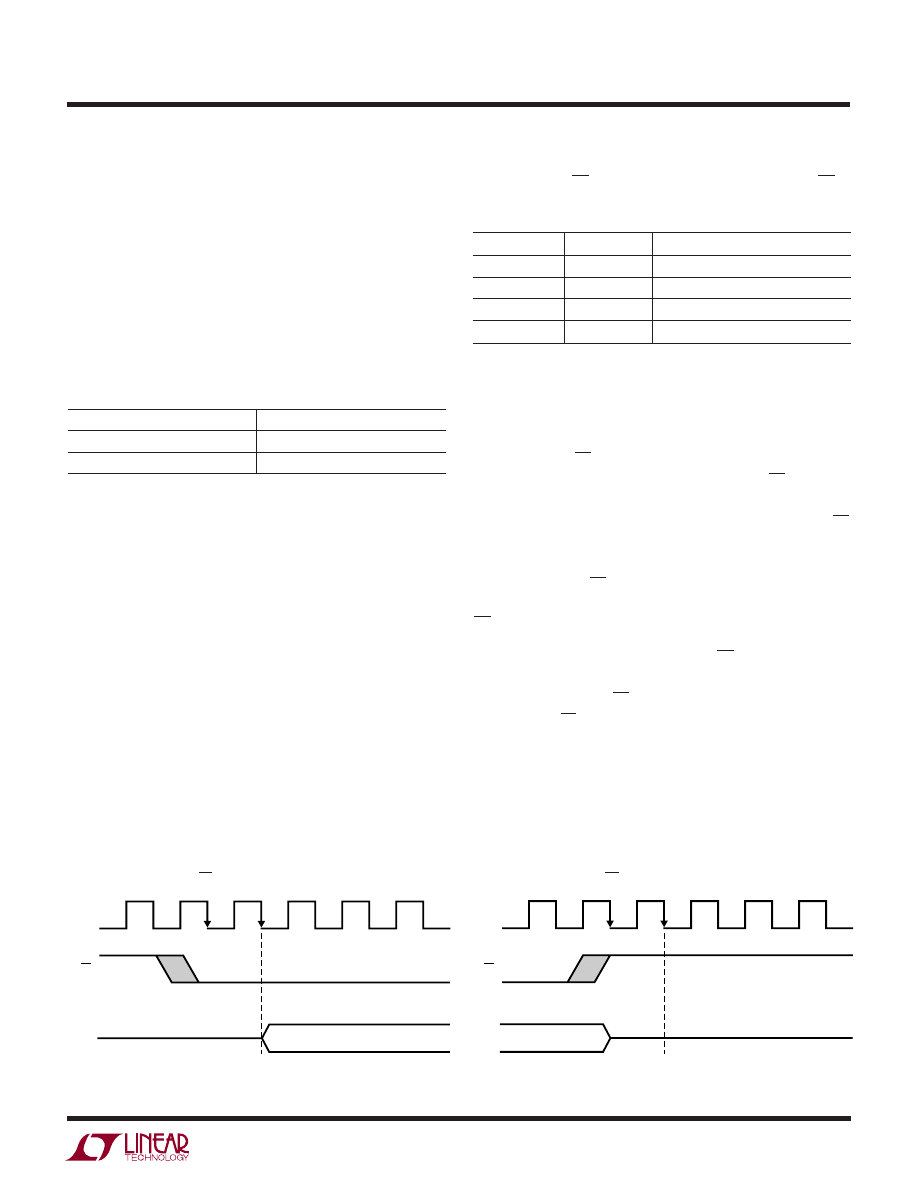
CS Low During Conversion
In the normal mode of operation, CS is brought high
during the conversion time. The serial port ignores any
SCLK activity while CS is high. The LTC1290 will also
operate with CS low during the conversion. In this mode,
SCLK must remain low during the conversion as shown in
the following figure. After the conversion is complete, the
D
OUT
line will become active with the first output bit. Then
the data transfer can begin as normal.
Low CS Recognized Internally
High CS Recognized Internally
D
OUT
CS
LTC1290 • AI07
ACLK
VALID OUTPUT
HI-Z
D
OUT
CS
LTC1290 • AI06
ACLK
VALID OUTPUT
HI-Z
14
LTC1290
1290fe
U
S
A
O
PPLICATI
W
U
U
I FOR ATIO
Figure 2. Data Output (D
OUT
) Timing with Different Word Lengths
tSMPL
B11
1
8
tCONV
B10
B9
B8
B7
B4
(SB)
8-Bit Word Length
SCLK
CS
D
OUT
LSB-FIRST
tSMPL
B11
1
tCONV
(SB)
12-Bit Word Length
SCLK
CS
D
OUT
LSB-FIRST
10
12
D
OUT
MSB-FIRST
D
OUT
MSB-FIRST
(SB)
tSMPL
1
tCONV
16-Bit Word Length
12
16
FILL
ZEROS
*
*
*
* IN UNIPOLAR MODE, THESE BITS ARE FILLED WITH ZEROS.
IN BIPOLAR MODE, THE SIGN BIT IS EXTENDED INTO THESE LOCATIONS.
LTC1290 F02
B6
B5
B0
B1
B2
B3
B4
B7
B5
B6
B10
B9
B8
B7
B6
B5
B4
B3
B2
B1
B0
B0
B1
B2
B3
B4
B5
B6
B7
B8
B9
B10
B11
SCLK
CS
D
OUT
LSB-FIRST
D
OUT
MSB-FIRST
B11
(SB)
(SB)
B10
B9
B8
B7
B6
B5
B4
B3
B2
B1
B0
B0
B1
B2
B3
B4
B5
B6
B7
B8
B9
B10
B11
THE LAST FOUR BITS
ARE TRUNCATED
15
LTC1290
1290fe
U
S
A
O
PPLICATI
W
U
U
I FOR ATIO
Microprocessor Interfaces
The LTC1290 can interface directly (without external hard-
ware) to most popular microprocessor (MPU) synchro-
nous serial formats (see Table 2). If an MPU without a
serial interface is used, then four of the MPU’s parallel port
lines can be programmed to form the serial link to the
LTC1290. Included here are two serial interface examples
and one example showing a parallel port programmed to
form the serial interface
Serial Port Microprocessors
Most synchronous serial formats contain a shift clock
(SCLK) and two data lines, one for transmitting and one for
receiving. In most cases data bits are transmitted on the
falling edge of the clock (SCLK) and captured on the rising
edge. However, serial port formats vary among MPU
manufactures as to the smallest number of bits that can be
sent in one group (e.g., 4-bit, 8-bit or 16-bit transfers).
They also vary as to the order in which the bits are
transmitted (LSB or MSB first). The following examples
show how the LTC1290 accommodates these differences.
Figure 4. CS Low During Conversion (CS Must go High to Low Once to Insure Proper Operation in this Mode)
B11 B10 B9
B8
B7
B6
B5
B4
B3
B2
B1
B0
B11 B10 B9
B8
B7
B6
B5
B4
B3
B2
B1
B0
SHIFT RESULT OUT
AND NEW ADDRESS IN
SCLK
CS
D
OUT
D
IN
t
SMPL
SAMPLE ANALOG
INPUT
SHIFT
MUX ADDRESS
IN
LTC1290 F04
48 TO 52
ACLK CYC
SCLK MUST
REMAIN LOW
DON’T CARE
Figure 3. CS High During Conversion
B11 B10 B9
B8
B7
B6
B5
B4
B3
B2
B1
B0
B11 B10 B9
B8
B7
B6
B5
B4
B3
B2
B1
B0
SHIFT RESULT OUT
AND NEW ADDRESS IN
SCLK
CS
D
OUT
D
IN
t
SMPL
SAMPLE ANALOG
INPUT
SHIFT
MUX ADDRESS
IN
LTC1290 F03
48 TO 52
ACLK CYC
DON’T CARE
16
LTC1290
1290fe
U
S
A
O
PPLICATI
W
U
U
I FOR ATIO
MICROWIRE and MICROWIRE PLUS are trademarks of National Semiconductor Corp
LTC1290 • AI08
SCLK
DOUT
LTC1290
CS
ANALOG
INPUTS
GO
SK
SI
COP402
DIN
SO
B6
B5
B4
B7
FIRST 4 BITS
SECOND 4 BITS
B10
B9
B8
B11
D
OUT
from LTC1290 Stored in COP402 RAM
MSB
†
LOCATION $13
LOCATION $14
B2
B1
B0
B3
THIRD 4 BITS
LSB
LOCATION $15
•
•
•
•
†
B11 IS MSB IN UNIPOLAR OR SIGN BIT IN BIPOLAR
National MICROWIRE (COP402)
The COP402 transfers data MSB first and in 4-bit incre-
ments (nibbles). This is easily accommodated by setting
the LTC1290 to MSB-first format and 12-bit word length.
The data output word is then received by the COP402 in
three 4-bit blocks.
COP402 Code
MNEMONIC
COMMENTS
CLRA
Must be First Instruction
LBI
1,0
BR = 1BD = 0 Initialize B Reg.
STII 8
First D
IN
Nibble in $10
STII E
Second D
IN
Nibble in $11
STII 0
Null Data in $12, B = $13
LEI
C
Set EN to (1100) BIN
LOOP
SC
Carry Set
LDD 1,0
Load First D
IN
Nibble In ACC
OGI
0
Go (CS) Cleared
XAS
ACC to Shift Reg. Begin Shift
LDD 1,1
Load Next D
IN
Nibble in ACC
NOP
Timing
XAS
Next Nibble, Shift Continues
XIS
0
First Nibble D
OUT
to $13
LDD 1,2
Put Null Data in ACC
XAS
Shift Continues, D
OUT
to ACC
XIS
0
Next Nibble D
OUT
to $14
RC
Clear Carry
CLRA
Clear ACC
XAS
Third Nibble D
OUT
to ACC
OGI
1
Go (CS) Set
XIS
0
Third Nibble D
OUT
to $15
LBI
1,3
Set B Reg. For Next Loop
Motorola SPI (MC68HC05C4)
The MC68HC05C4 transfers data MSB first and in 8-bit
increments. Programming the LTC1290 for MSB-first
format and 16-bit word length allows the 12-bit data
output to be received by the MPU as two 8-bit bytes with
the final four unused bits filled with zeros by the LTC1290.
Hardware and Software Interface to COP402 Processor
Table 2. Microprocessors with Hardware Serial Interfaces
Compatible with the LTC1290**
PART NUMBER
TYPE OF INTERFACE
Motorola
MC6805S2, S3
SPI
MC68HC11
SPI
MC68HC05
SPI
RCA
CDP68HC05
SPI
Hitachi
HD6305
SCI Synchronous
HD6301
SCI Synchronous
HD63701
SCI Synchronous
HD6303
SCI Synchronous
HD64180
SCI Synchronous
National Semiconductor
COP400 Family
MICROWIRE
TM
COP800 Family
MICROWIRE/PLUS
TM
NS8050U
MICROWIRE/PLUS
HPC16000 Family
MICROWIRE/PLUS
Texas Instruments
TMS7002
Serial Port
TMS7042
Serial Port
TMS70C02
Serial Port
TMS70C42
Serial Port
TMS32011*
Serial Port
TMS32020
Serial Port
TMS370C050
SPI
*Requires external hardware
** Contact factory for interface information for processors not on this list
17
LTC1290
1290fe
U
S
A
O
PPLICATI
W
U
U
I FOR ATIO
Hardware and Software Interface to Motorola
MC68HC05C4 Processor
LTC1290 • AI09
SCLK
DOUT
LTC1290
CS
ANALOG
INPUTS
CO
SCK
MISO
MC68HC05C4
DIN
MOSI
BYTE 1
B10
B9
B8
B11
B6
B5
B4
B7
D
OUT
from LTC1290 Stored in MC68HC05C4 RAM
MSB*
LOCATION $61
BYTE 2
B2
B1
B0
B3
0
0
0
0
LSB
LOCATION $62
•
•
•
•
*B11 IS MSB IN UNIPOLAR OR SIGN BIT IN BIPOLAR
MC68HC05C4 Code
MNEMONIC
COMMENTS
LDA #$50
Configuration Data for SPCR
STA $0A
Load Data Into SPCR ($0A)
LDA #$FF
Config. Data for Port C DDR
STA $06
Load Data Into Port C DDR
LDA #$0F
Load LTC1290 D
IN
Data Into ACC
STA $50
Load LTC1290 D
IN
Data Into $50
START
BCLR 0,$20
CO Goes Low (CS Goes Low)
LDA $50
Load D
IN
Into ACC from $50
STA $0C
Load D
IN
Into SPI, Start SCK
NOP
8 NOPs for Timing
LDA $0B
Check SPI Status Reg
LDA $0C
Load LTC1290 MSBs Into ACC
STA $61
Store MSBs in $61
STA $0C
Start Next SPI Cycle
NOP
6 NOPs for Timing
BSET 0,$02
CO Goes High (CS Goes High)
LDA $0B
Check SPI Status Register
LDA $0C
Load LTC1290 LSBs Into ACC
STA $62
Store LSBs in $62
Parallel Port Microprocessors
When interfacing the LTC1290 to an MPU which has a
parallel port, the serial signals are created on the port with
software. Three MPU port lines are programmed to create
the CS, SCLK and D
IN
signals for the LTC1290. A fourth
port line reads the D
OUT
line. An example is made of the
Intel 8051/8052/80C252 family.
Intel 8051
To interface to the 8051, the LTC1290 is programmed for
MSB-first format and 12-bit word length. The 8051 gener-
ates CS, SCLK and D
IN
on three port lines and reads D
OUT
on the fourth.
Hardware and Software Interface to Intel 8051 Processor
LTC1290 • AI10
DIN
CS
ACLK
LTC1290
DOUT
ANALOG
INPUTS
P1.1
P1.2
P1.4
ALE
8051
SCLK
P1.3
B10
B9
B8
B11
B6
B5
54
B7
D
OUT
from LTC1290 Stored in 8051 RAM
MSB*
R2
B2
B1
B0
B3
0
0
0
0
LSB
R3
•
•
•
•
•
•
•
•
*B11 IS MSB IN UNIPOLAR OR SIGN BIT IN BIPOLAR
18
LTC1290
1290fe
U
S
A
O
PPLICATI
W
U
U
I FOR ATIO
8051 Code
MNEMONIC
COMMENTS
MOV P1,#02H
Bit 1 Port 1 Set as Input
CLR P1.3
SCLK Goes Low
SETB P1.4
CS Goes High
CONT
MOV A,#0EH
D
IN
Word for LTC1290
CLR P1.4
CS Goes Low
MOV R4,#08H
Load Counter
NOP
Delay for Deglitcher
LOOP
MOV C,P1.1
Read Data Bit Into Carry
RLC A
Rotate Data Bit Into ACC
MOV P1.2,C
Output D
IN
Bit to LTC1290
SETB P1.3
SCLK Goes High
CLR P1.3
SCLK Goes Low
DJNZ R4,LOOP
Next Bit
MOV R2,A
Store MSBs in R2
MOV C,P1.1
Read Data Bit Into Carry
CLR A
Clear ACC
RLC A
Rotate Data Bit Into ACC
SETB P1.3
SCLK Goes High
CLR P1.3
SCLK Goes Low
MOV C,P1.1
Read Data Bit Into Carry
RLC A
Rotate Data Bit Into ACC
SETB P1.3
SCLK Goes High
CLR P1.3
SCLK Goes Low
MOV C,P1.1
Read Data Bit Into Carry
RLC A
Rotate Data Bit Into ACC
SETB P1.3
SCLK Goes High
CLR P1.3
SCLK Goes Low
MOV C, P1.1
Read Data Bit Into Carry
RRC A
Rotate Right Into ACC
RRC A
Rotate Right Into ACC
RRC A
Rotate Right Into ACC
RRC A
Rotate Right Into ACC
MOV R3,A
Store LSBs in R3
SETB P1.3
SCLK Goes High
CLR P1.3
SCLK Goes Low
SETB P1.4
CS Goes High
MOV R5,#0BH
Load Counter
DELAY
DJNZ R5,DELAY
Go to Delay if Not Done
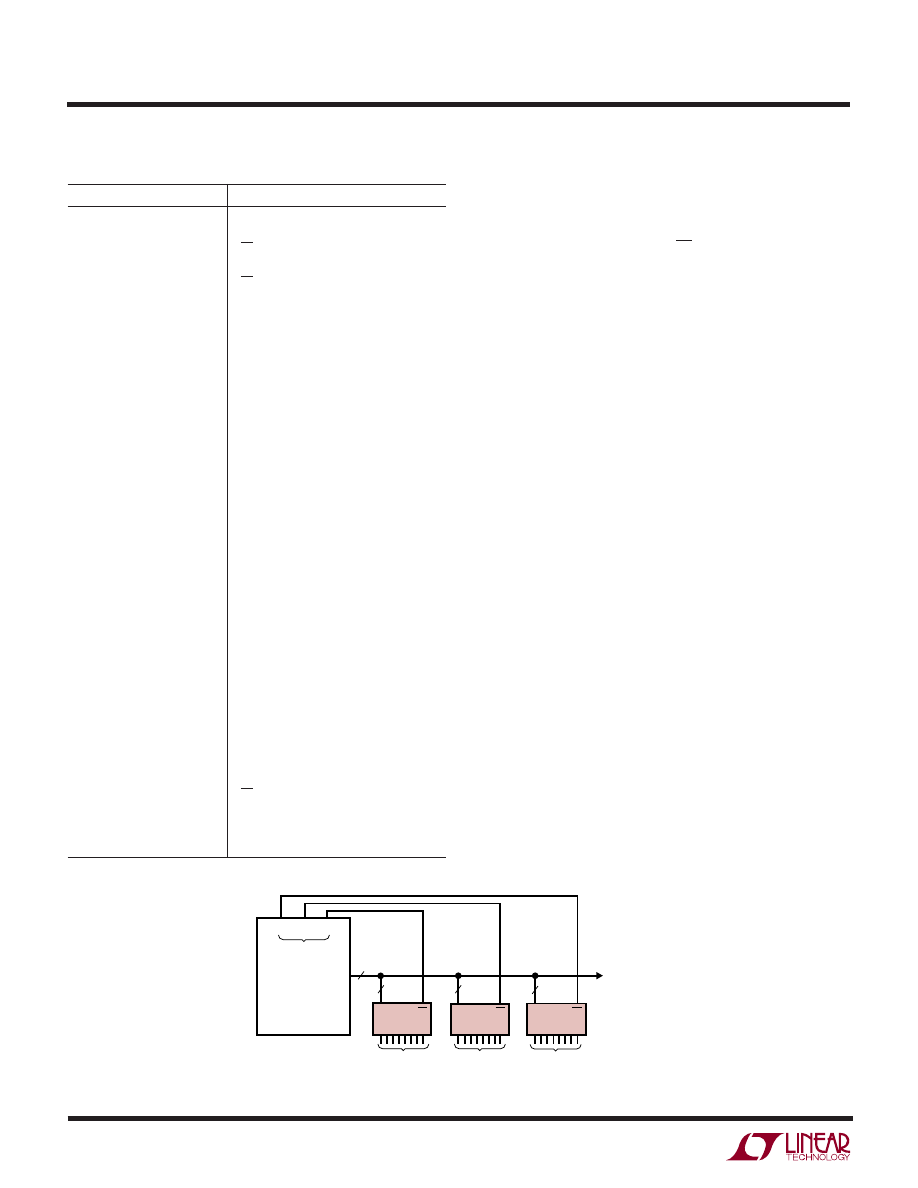
8 CHANNELS
8 CHANNELS
8 CHANNELS
3
3
3
3
3-WIRE SERIAL
INTERFACE TO OTHER
PERIPHERALS OR LTC1290s
2
1
0
OUTPUT PORT
SERIAL DATA
MPU
LTC1290 F05
LTC1290
CS
LTC1290
CS
LTC1290
CS
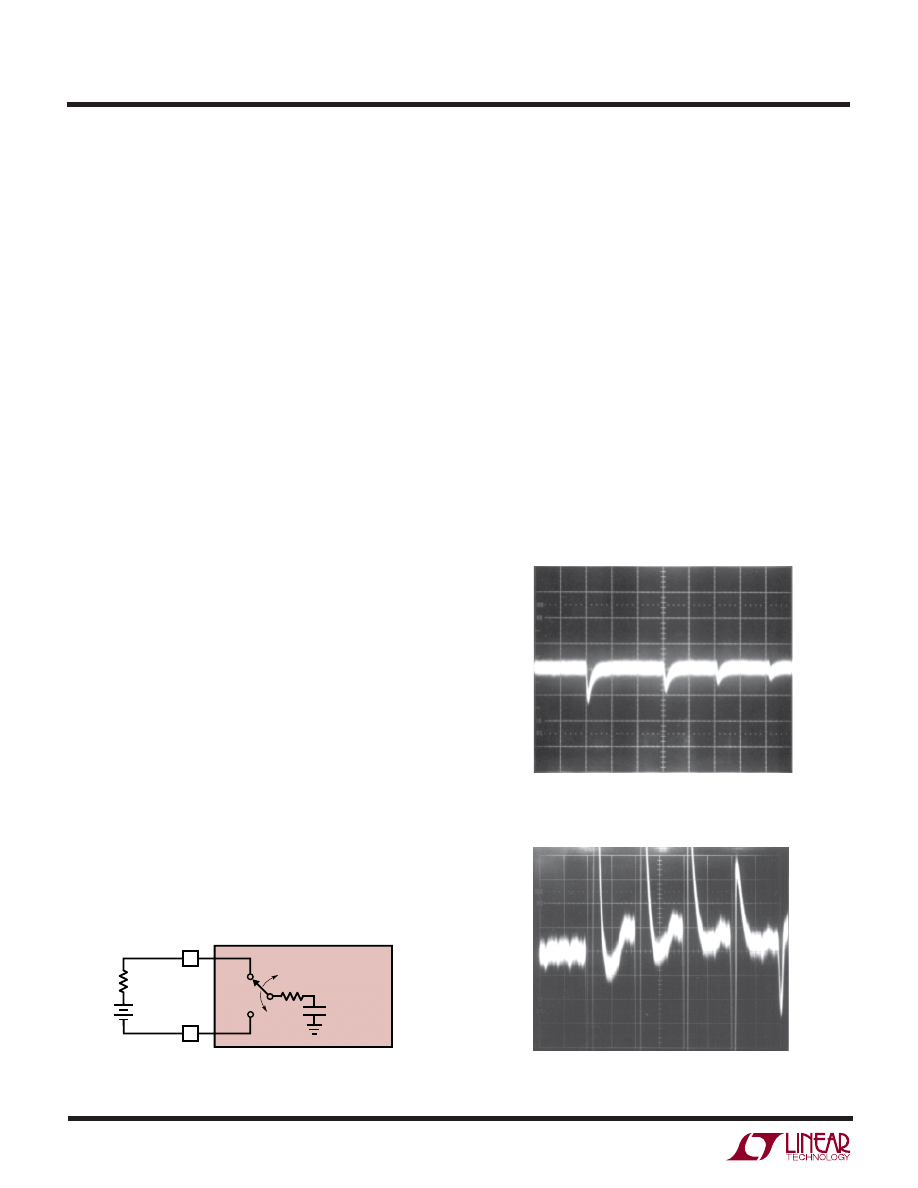
Sharing the Serial Interface
The LTC1290 can share the same 3-wire serial interface
with other peripheral components or other LTC1290s (see
Figure 5). In this case, the CS signals decide which
LTC1290 is being addressed by the MPU.
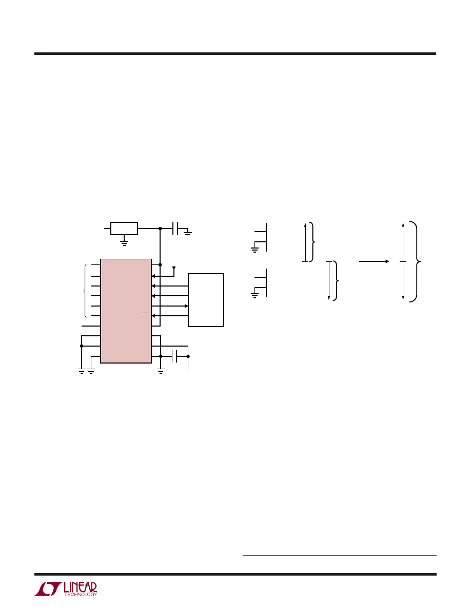
ANALOG CONSIDERATIONS
1. Grounding
The LTC1290 should be used with an analog ground plane
and single point grounding techniques.
AGND (Pin 11) should be tied directly to this ground plane.
DGND (Pin 10) can also be tied directly to this ground
plane because minimal digital noise is generated within
the chip itself.
V
CC
(Pin 20) should be bypassed to the ground plane with
a 22
µF tantalum with leads as short as possible. V
–
(Pin
12) should be bypassed with a 0.1
µF ceramic disk. For
single supply applications, V
–
can be tied to the ground
plane.
It is also recommended that REF
–
(Pin 13) and COM (Pin
9) be tied directly to the ground plane. All analog inputs
should be referenced directly to the single point ground.
Digital inputs and outputs should be shielded from and/or
routed away from the reference and analog circuitry.
Figure 5. Several LTC1290s Sharing One 3-Wire Serial Interface
19
LTC1290
1290fe
V
–
22
µF
TANTALUM
V
CC
LTC1290 F06
0.1
µF
CERAMIC
DISK
ANALOG
GROUND
PLANE
1
10
20
U
S
A
O
PPLICATI
W
U
U
I FOR ATIO
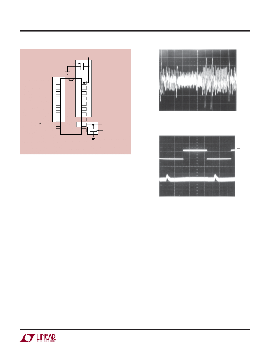
Figure 6. Example Ground Plane for the LTC1290
Figure 6 shows an example of an ideal ground plane design
for a two-sided board. Of course, this much ground plane
will not always be possible, but users should strive to get
as close to this ideal as possible.
2. Bypassing
For good performance, V
CC
must be free of noise and
ripple. Any changes in the V
CC
voltage with respect to
analog ground during a conversion cycle can induce
errors or noise in the output code. V
CC
noise and ripple can
be kept below 0.5mV by bypassing the V
CC
pin directly to
the analog ground plane with a 22
µF tantalum capacitor
and leads as short as possible. The lead from the device to
the V
CC
supply should also be kept to a minimum and the
V
CC
supply should have a low output impedance such as
that obtained from a voltage regulator (e.g., LT1761).
Figures 7 and 8 show the effects of good and poor V
CC
bypassing.
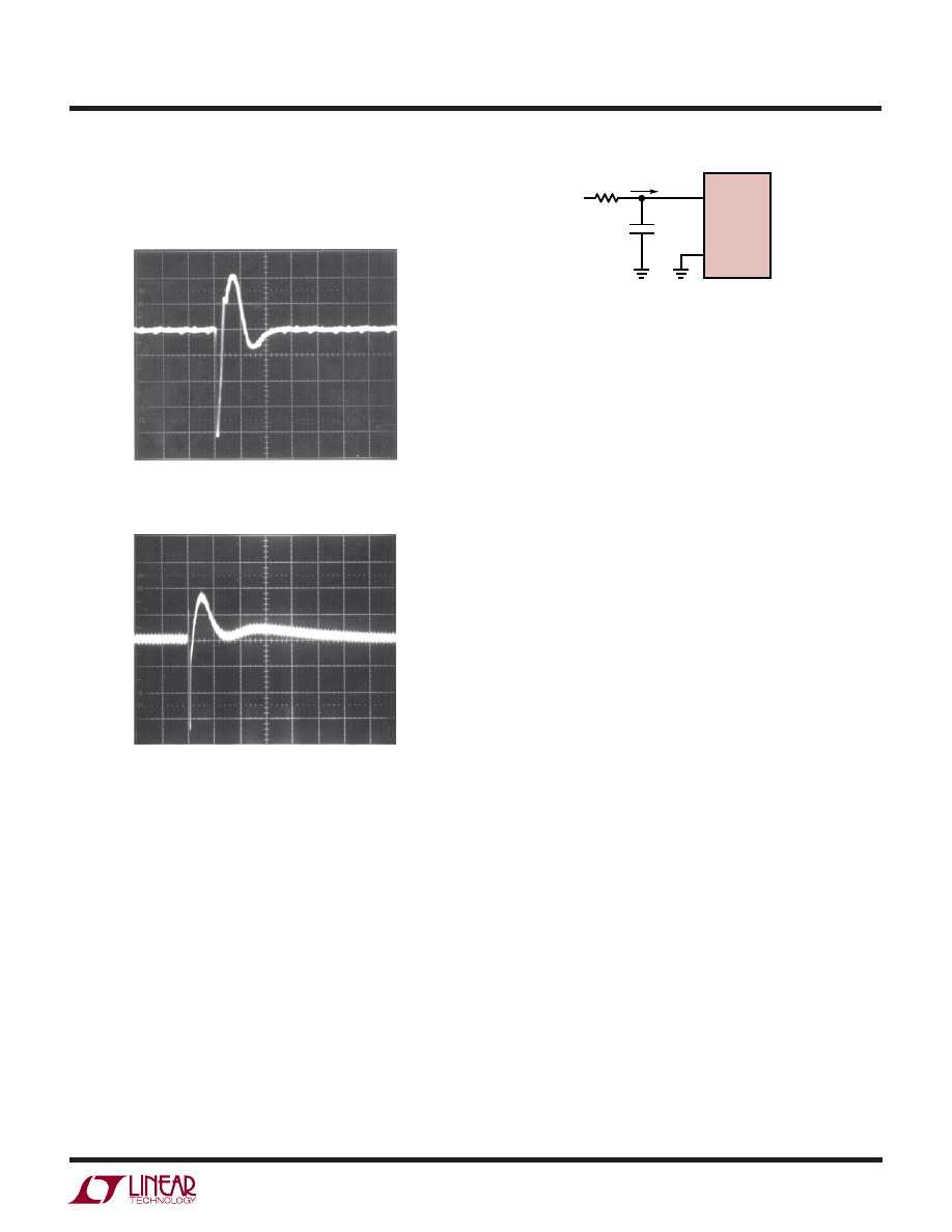
3. Analog Inputs
Because of the capacitive redistribution A/D conversion
techniques used, the analog inputs of the LTC1290 have
capacitive switching input current spikes. These current
Figure 7. Poor V
CC
Bypassing.
Noise and Ripple Can Cause A/D Errors
VERTICAL: 0.5mV/DIV
HORIZONTAL: 10
µs/DIV
CS
V
CC
Figure 8. Good V
CC
Bypassing Keeps
Noise and Ripple on V
CC
Below 1mV
HORIZONTAL: 10
µs/DIV
VERTICAL: 0.5mV/DIV
spikes settle quickly and do not cause a problem. How-
ever, if large source resistances are used or if slow settling
op amps drive the inputs, care must be taken to insure that
the transients caused by the current spikes settle com-
pletely before the conversion begins.
Source Resistance
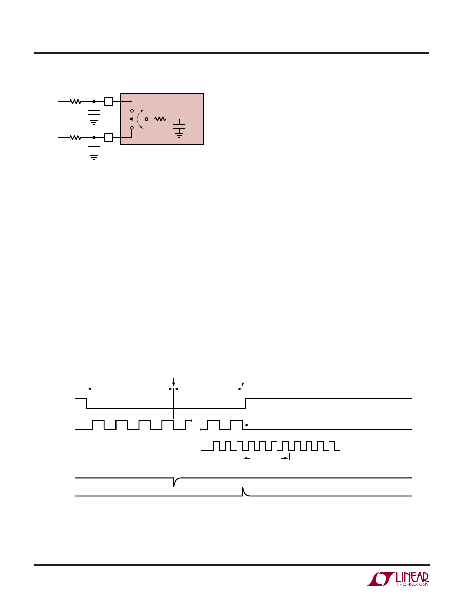
The analog inputs of the LTC1290 look like a 100pF
capacitor (C
IN
) in series with a 500
Ω resistor (R
ON
) as
shown in Figure 9. C
IN
gets switched between the selected
“+” and “–” inputs once during each conversion cycle. Large
external source resistors and capacitances will slow the
settling of the inputs. It is important that the overall RC time
constants be short enough to allow the analog inputs to
completely settle within the allowed time.
20
LTC1290
1290fe
U
S
A
O
PPLICATI
W
U
U
I FOR ATIO
4TH SCLK
R
ON
= 500
Ω
LAST SCLK
C
IN
=
100pF
LTC1290
“+”
INPUT
R
SOURCE
+
V
IN
+
C1
“–”
INPUT
R
SOURCE
–
V
IN
–
C2
LTC1290 F09
Figure 9. Analog Input Equivalent Circuit
“+” Input Settling
This input capacitor is switched onto the “+” input during
the sample phase (t
SMPL
, see Figure 10). The sample
phase starts at the 4th SCLK cycle and lasts until the falling
edge of the last SCLK (the 8th, 12th or 16th SCLK cycle
depending on the selected word length). The voltage on
the “+” input must settle completely within this sample
time. Minimizing R
SOURCE
+
and C1 will improve the input
settling time. If large “+” input source resistance must be
used, the sample time can be increased by using a slower
SCLK frequency or selecting a longer word length. With
the minimum possible sample time of 2
µs, R
SOURCE
+
< 1k
and C1 < 20pF will provide adequate settling.
“–” Input Settling
At the end of the sample phase the input capacitor switches
to the “–” input and the conversion starts (see Figure 10).
During the conversion, the “+” input voltage is effectively
“held” by the sample-and-hold and will not affect the
conversion result. However, it is critical that the “–” input
voltage be free of noise and settle completely during the
first four ACLK cycles of the conversion time. Minimizing
R
SOURCE
–
and C2 will improve settling time. If large “–”
input source resistance must be used, the time allowed for
settling can be extended by using a slower ACLK fre-
quency. At the maximum ACLK rate of 4MHz, R
SOURCE
–
< 250
Ω
and C2 < 20pF will provide adequate settling.
Input Op Amps
When driving the analog inputs with an op amp it is
important that the op amp settle within the allowed time
(see Figure 10). Again, the “+” and “–” input sampling
times can be extended as described above to accommo-
date slower op amps. Most op amps including the LT1797,
LT1800 and LT1812 single supply op amps can be made
to settle well even with the minimum settling windows of
2
µs (“+” input) and 1µs (“–” input) which occur at the
SCLK
CS
“+” INPUT
ACLK
1290 • F10
1
2
3
4
• • •
• • •
• • •
MUX ADDRESS
SHIFTED IN
t
SMPL
LAST SCLK (8TH, 12TH OR 16TH DEPENDING ON WORD LENGTH)
1
2
3
4
1ST BIT TEST
“–” INPUT MUST SETTLE
DURING THIS TIME
SAMPLE
HOLD
“+” INPUT
MUST SETTLE
DURING THIS TIME
“–” INPUT
• • •
Figure 10. “+” and “–” Input Settling Windows
21
LTC1290
1290fe
U
S
A
O
PPLICATI
W
U
U
I FOR ATIO
maximum clock rates (ACLK = 4MHz and SCLK = 2MHz).
Figures 11 and 12 show examples of adequate and poor
op amp settling.
HORIZONTAL: 500ns/DIV
Figure 11. Adequate Settling of Op Amps Driving Analog Input
VERTICAL: 5mV/DIV
HORIZONTAL: 20
µs/DIV
Figure 12. Poor Op Amp Settling Can Cause A/D Errors
VERTICAL: 5mV/DIV
RC Input Filtering
It is possible to filter the inputs with an RC network as shown
in Figure 13. For large values of C
F
(e.g., 1
µF), the capacitive
input switching currents are averaged into a net DC current.
Therefore, a filter should be chosen with a small resistor and
large capacitor to prevent DC drops across the resistor. The
magnitude of the DC current is approximately I
DC
=
(100pF)(V
IN
/t
CYC
) and is roughly proportional to V
IN
. When
running at the minimum cycle time of 20
µs, the input
current equals 25
µA at V
IN
= 5V. In this case, a filter resistor
of 5
Ω will cause 0.1LSB of full-scale error. If a larger filter
resistor must be used, errors can be eliminated by increas-
ing the cycle time as shown in the typical curve of Maximum
Filter Resistor vs Cycle Time.
Figure 13. RC Input Filtering
R
FILTER
V
IN
C
FILTER
LTC1290 F13
LTC1290
"+"
"–"
I
DC
Input Leakage Current
Input leakage currents can also create errors if the source
resistance gets too large. For instance, the maximum input
leakage specification of 1
µA (at 125°C) flowing through a
source resistance of 1k
Ω will cause a voltage drop of 1mV
or 0.8LSB. This error will be much reduced at lower
temperatures because leakage drops rapidly (see the
typical curve of Input Channel Leakage Current vs Tem-
perature).
Noise Coupling Into Inputs
High source resistance input signals (>500
Ω) are more
sensitive to coupling from external sources. It is prefer-
able to use channels near the center of the package (i.e.,
CH2 to CH7) for signals which have the highest output
resistance because they are essentially shielded by the
pins on the package ends (DGND and CH0). Grounding
any unused inputs (especially the end pin, CH0) will also
reduce outside coupling into high source resistances.
4. Sample-and-Hold
Single-Ended Inputs
The LTC1290 provides a built-in sample-and-hold (S&H)
function for all signals acquired in the single-ended mode
(COM pin grounded). This sample-and-hold allows the
LTC1290 to convert rapidly varying signals (see the typical
curve of S&H Acquisition Time vs Source Resistance). The
input voltage is sampled during the t
SMPL
time as shown in
Figure 10. The sampling interval begins after the fourth MUX
address bit is shifted in and continues during the remainder
of the data transfer. On the falling edge of the final SCLK, the
S&H goes into hold mode and the conversion begins. The
voltage will be held on either the 8th, 12th or 16th falling edge
of the SCLK depending on the word length selected.
22
LTC1290
1290fe
U
S
A
O
PPLICATI
W
U
U
I FOR ATIO
Differential Inputs
With differential inputs or when the COM pin is not tied to
ground, the A/D no longer converts just a single voltage but
rather the difference between two voltages. In these cases,
the voltage on the selected “+” input is still sampled and held
and therefore may be rapidly time varying just as in single-
ended mode. However, the voltage on the selected “–” input
must remain constant and be free of noise and ripple
throughout the conversion time. Otherwise, the differencing
operation may not be performed accurately. The conversion
time is 52 ACLK cycles. Therefore, a change in the “–” input
voltage during this interval can cause conversion errors.
For a sinusoidal voltage on the “–” input this error would be:
V
ERROR (MAX)
= (V
PEAK
)(2
π)[ f(“–”)](52/f
ACLK
)
Where f(“–”) is the frequency of the “–” input voltage,
V
PEAK
is its peak amplitude and f
ACLK
is the frequency of
the ACLK. In most cases V
ERROR
will not be significant. For
a 60Hz signal on the “–” input to generate a 0.25LSB error
(300
µV) with the converter running at ACLK = 4MHz, its
peak value would have to be 61mV.
5. Reference Inputs
The voltage between the reference inputs of the LTC1290
defines the voltage span of the A/D converter. The refer-
ence inputs will have transient capacitive switching cur-
rents due to the switched capacitor conversion technique
(see Figure 14). During each bit test of the conversion
(every 4 ACLK cycles), a capacitive current spike will be
generated on the reference pins by the A/D. These current
spikes settle quickly and do not cause a problem. How-
ever, if slow settling circuitry is used to drive the reference
inputs, care must be taken to insure that transients caused
by these current spikes settle completely during each bit
test of the conversion.
Figure 14. Reference Input Equivalent Circuit
R
ON
8pF TO 40pF
LTC1290
REF+
R
OUT
V
REF
EVERY 4 ACLK CYCLES
14
13
REF–
LTC 1290 F14
When driving the reference inputs, two things should be
kept in mind:
1. Transients on the reference inputs caused by the
capacitive switching currents must settle completely
during each bit test (each 4 ACLK cycles). Figures 15
and 16 show examples of both adequate and poor
settling. Using a slower ACLK will allow more time for
the reference to settle. However, even at the maximum
ACLK rate of 4MHz most references and op amps can
be made to settle within the 1
µs bit time. For example
the LT1236 will settle adequately.
2. It is recommended that REF
–
input be tied directly to
the analog ground plane. If REF
–
is biased at a voltage
other than ground, the voltage must not change during
a conversion cycle. This voltage must also be free of
noise and ripple with respect to analog ground.
Figure 16. Poor Reference Settling Can Cause A/D Errors
HORIZONTAL: 1
µs/DIV
VERTICAL: 0.5mV/DIV
Figure 15. Adequate Reference Settling
HORIZONTAL: 1
µs/DIV
VERTICAL: 0.5mV/DIV

23
LTC1290
1290fe
U
S
A
O
PPLICATI
W
U
U
I FOR ATIO
6. Reduced Reference Operation
The effective resolution of the LTC1290 can be increased
by reducing the input span of the converter. The LTC1290
exhibits good linearity and gain over a wide range of
reference voltages (see the typical curves of Linearity and
Gain Error vs Reference Voltage). However, care must be
taken when operating at low values of V
REF
because of the
reduced LSB step size and the resulting higher accuracy
requirement placed on the converter. The following factors
must be considered when operating at low V
REF
values:
1. Offset
2. Noise
Offset with Reduced V
REF
The offset of the LTC1290 has a larger effect on the output
code when the A/D is operated with reduced reference
voltage. The offset (which is typically a fixed voltage)
becomes a larger fraction of an LSB as the size of the LSB
is reduced. The typical curve of Unadjusted Offset Error vs
Reference Voltage shows how offset in LSBs is related to
reference voltage for a typical value of V
OS
. For example,
a V
OS
of 0.1mV which is 0.1LSB with a 5V reference
becomes 0.4LSB with a 1.25V reference. If this offset is
unacceptable, it can be corrected digitally by the receiving
system or by offsetting the “–” input to the LTC1290.
Noise with Reduced V
REF
The total input referred noise of the LTC1290 can be
reduced to approximately 200
µV peak-to-peak using a
ground plane, good bypassing, good layout techniques
and minimizing noise on the reference inputs. This noise
is insignificant with a 5V reference but will become a larger
fraction of an LSB as the size of the LSB is reduced. The
typical curve of Noise Error vs Reference Voltage shows
the LSB contribution of this 200
µV of noise.
For operation with a 5V reference, the 200
µV noise is only
0.16LSB peak-to-peak. In this case, the LTC1290 noise
will contribute virtually no uncertainty to the output code.
However, for reduced references, the noise may become
a significant fraction of an LSB and cause undesirable jitter
in the output code. For example, with a 1.25V reference,
this same 200
µV noise is 0.64LSB peak-to-peak. This will
reduce the range of input voltages over which a stable
output code can be achieved by 0.64LSB. In this case
averaging readings may be necessary.
This noise data was taken in a very clean setup. Any setup in-
duced noise (noise or ripple on V
CC
, V
REF
, V
IN
or V
–
) will add to
the internal noise. The lower the reference voltage to be used,
the more critical it becomes to have a clean, noise-free setup.
7. LTC1290 AC Characteristics
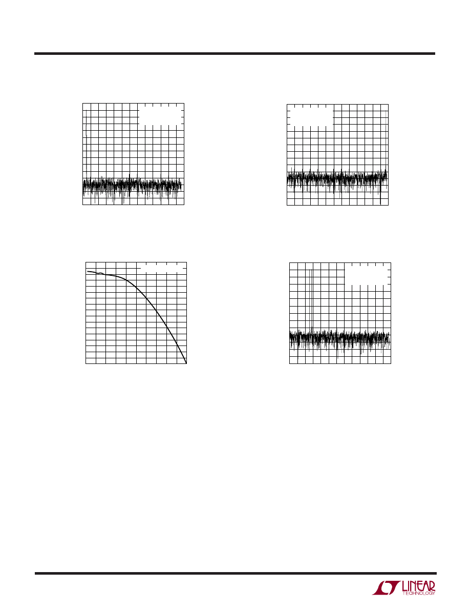
Two commonly used figures of merit for specifying the
dynamic performance of the A/D’s in digital signal process-
ing applications are the Signal-to-Noise Ratio (SNR) and
the “effective number of bits (ENOB).” SNR is defined as
the ratio of the RMS magnitude of the fundamental to the
RMS magnitude of all the nonfundamental signals up to the
Nyquist frequency (half the sampling frequency). The
theoretical maximum SNR for a sine wave input is given by:
SNR = (6.02N + 1.76dB)
where N is the number of bits. Thus the SNR is a function
of the resolution of the A/D. For an ideal 12-bit A/D the SNR
is equal to 74dB. A Fast Fourier Transform(FFT) plot of the
output spectrum of the LTC1290 is shown in Figures 17a
and 17b. The input (f
IN
) frequencies are 1kHz and 25kHz
with the sampling frequency (f
S
) at 50.6kHz. The SNR
obtained from the plot are 73.25dB and 72.54dB.
Rewriting the SNR expression it is possible to obtain the
equivalent resolution based on the SNR measurement.
N = (SNR – 1.76dB)/6.02
This is the so-called effective number of bits (ENOB). For
the example shown in Figures 17a and 17b, N = 11.9 bits
and 11.8 bits, respectively. Figure 18 shows a plot of ENOB
as a function of input frequency. The curve shows the
A/D’s ENOB remain in the range of 11.9 to 11.8 for input
frequencies up to f
S
/2.
Figure 19 shows an FFT plot of the output spectrum for two
tones applied to the input of the A/D. Nonlinearities in the
A/D will cause distortion products at the sum and differ-
ence frequencies of the fundamentals and products of the
fundamentals. This is classically referred to as intermod-
ulation distortion (IMD).
24
LTC1290
1290fe
U
S
A
O
PPLICATI
W
U
U
I FOR ATIO
FREQUENCY (kHz)
0
8
12
16
20
4
24
MAGNITUDE (dB)
1290 • F17a
0
–20
–40
–60
–80
–100
–120
–140
f
IN
= 1kHz
f
SAMPLE
= 50.6kHz
SNR = 73.25dB
Figure 17a. LTC1290 FFT Plot
FREQUENCY (kHz)
0
8
12
16
20
4
24
MAGNITUDE (dB)
1290 • F17b
0
–20
–40
–60
–80
–100
–120
–140
f
IN
= 25kHz
f
SAMPLE
= 50.6kHz
SNR = 72.54dB
Figure 17b. LTC1290 FFT Plot
FREQUENCY (kHz)
0
EFFECTIVE NUMBER OF BITS
80
1290 F18
20
40
100
12
11.6
11.2
10.8
10.4
10
9.6
9.2
8.8
60
f
SAMPLE
= 50.6kHz
Figure 18. LTC1290 ENOB vs Input Frequency
Figure 19. LTC1290 FFT Plot
FREQUENCY (kHz)
0
8
12
16
20
4
24
MAGNITUDE (dB)
1290 • F19
0
–20
–40
–60
–80
–100
–120
f
IN1
= 5.1kHz
f
IN2
= 5.6kHz
f
SAMPLE
= 50.6kHz
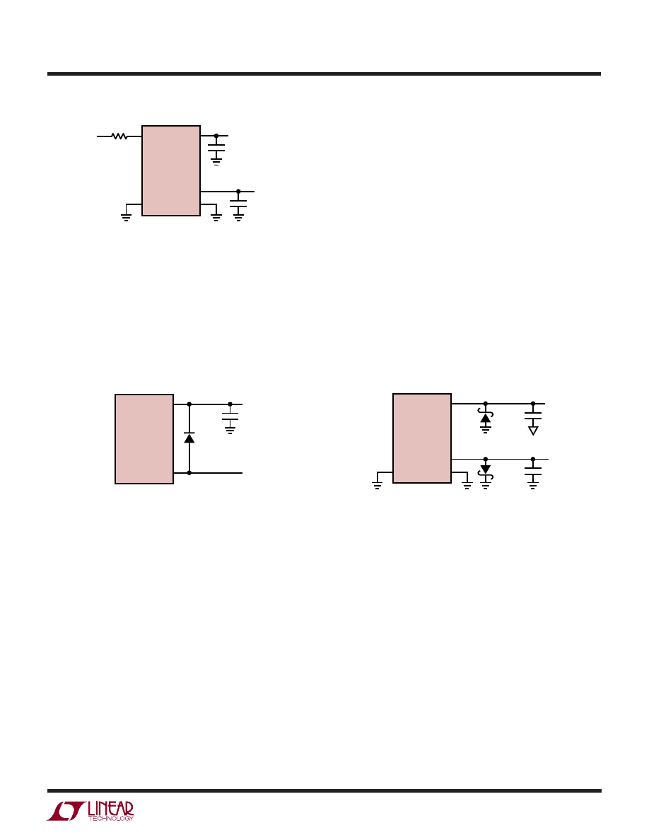
8. Overvoltage Protection
Applying signals to the analog MUX that exceed the
positive or negative supply of the device will degrade the
accuracy of the A/D and possibly damage the device. For
example this condition would occur if a signal is applied to
the analog MUX before power is applied to the LTC1290.
Another example is the input source is operating from
different supplies of larger value than the LTC1290. These
conditions should be prevented either with proper supply
sequencing or by use of external circuitry to clamp or
current limit the input source. As shown in Figure 20, a 1k
resistor is enough to stand off
±15V (15mA for one only
channel). If more than one channel exceeds the supplies
then the following guidelines can be used. Limit the
current to 7mA per channel and 28mA for all channels.
This means four channels can handle 7mA of input current
each. Reducing the ACLK and SCLK frequencies from the
maximum of 4MHz and 2MHz, respectively, (see Typical
Performance Characteristics curves Maximum ACLK Fre-
quency vs Source Resistance and Sample-and-Hold
Acquisition Time vs Source Resistance) allows the use of
larger current limiting resistors. Use 1N4148 diode clamps
from the MUX inputs to V
CC
and V
–
if the value of the series
resistor will not allow the maximum clock speeds to be
used or if an unknown source is used to drive the LTC1290
MUX inputs.
25
LTC1290
1290fe
U
S
A
O
PPLICATI
W
U
U
I FOR ATIO
How the various power supplies to the LTC1290 are
applied can also lead to overvoltage conditions. For single
supply operation (i.e., unipolar mode), if V
CC
and REF
+
are
not tied together, then V
CC
should be turned on first, then
REF
+
. If this sequence cannot be met, connecting a diode
from REF
+
to V
CC
is recommended (see Figure 21).
For dual supplies (bipolar mode) placing two Schottky
diodes from V
CC
and V
–
to ground (Figure 23) will prevent
power supply reversal from occurring when an input
source is applied to the analog MUX before power is
applied to the device. Power supply reversal occurs, for
example, if the input is pulled below V
–
then V
CC
will pull
a diode drop below ground which could cause the device
not to power up properly. Likewise, if the input is pulled
above V
CC
then V
–
will be pulled a diode drop above
ground. If no inputs are present on the MUX, the Schottky
diodes are not required if V
–
is applied first, then V
CC
.
Because a unique input protection structure is used on the
digital input pins, the signal levels on these pins can
exceed the device V
CC
without damaging the device.
5V
1290 F21
REF
+
V
CC
LTC1290
22
µF
1N4148
V
REF
14
20
5V
1290 F22
DGND
V
–
AGND
V
CC
LTC1290
–5V
0.1
µF
22
µF
1N5817
1N5817
Figure 21
Figure 22. Power Supply Reversal
Figure 20. Overvoltage Protection for MUX
5V
1290 F20
DGND
V
–
AGND
V
CC
1k
LTC1290
CH0
V
IN
–5V
0.1
µF
22
µF
26
LTC1290
1290fe
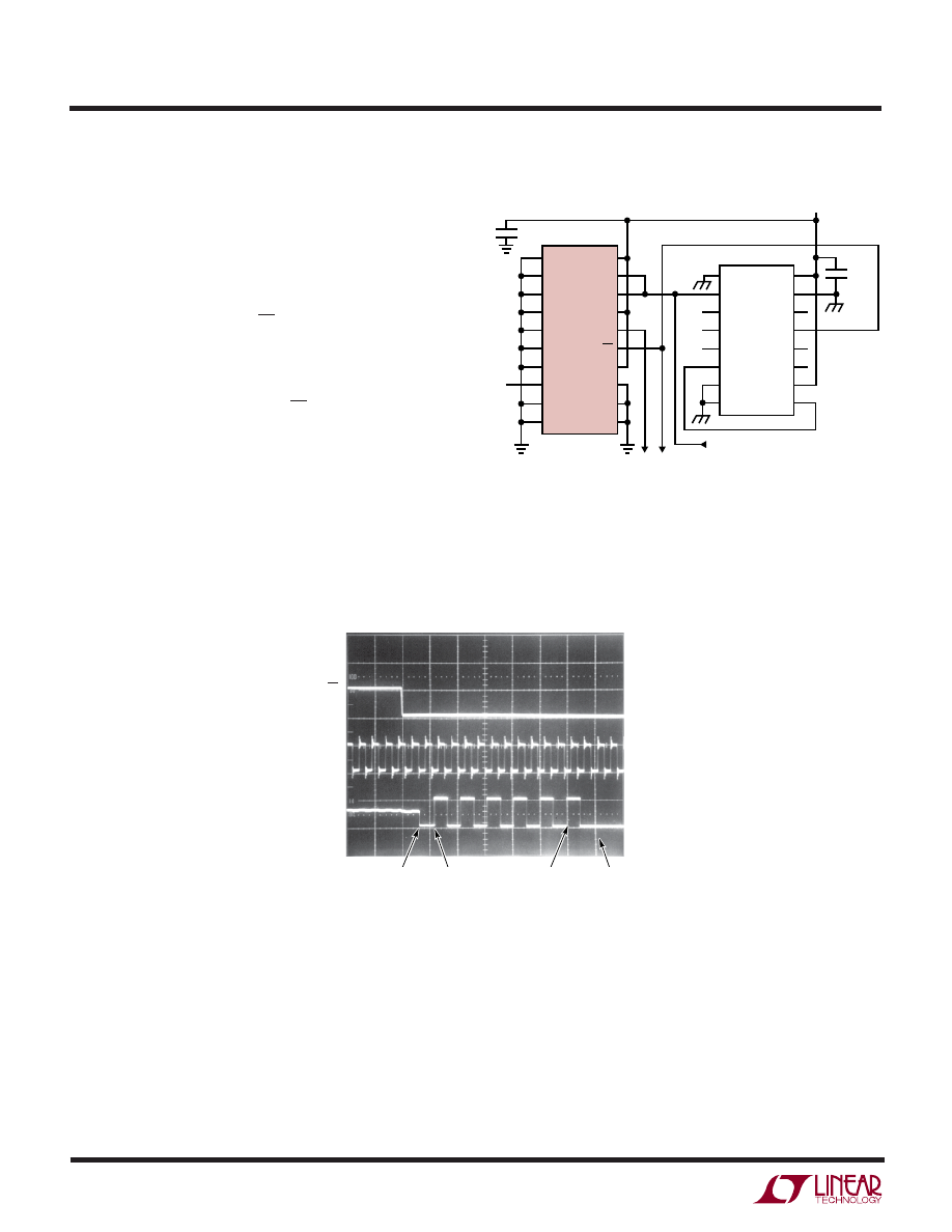
A “Quick Look” Circuit for the LTC1290
Users can get a quick look at the function and timing of the
LTC1290 by using the following simple circuit. REF
+
and
D
IN
are tied to V
CC
selecting a 5V input span, CH7 as a
single-ended input, unipolar mode, MSB-first format and
16-bit word length. ACLK and SCLK are tied together and
driven by an external clock. CS is driven at 1/128 the clock
rate by the CD4520 and D
OUT
outputs the data. All other
pins are tied to a ground plane. The output data from the
D
OUT
pin can be viewed on an oscilloscope which is set up
to trigger on the falling edge of CS.
U
S
A
O
PPLICATI
TYPICAL
A “Quick Look” Circuit for the LTC1290
1290 TA02
LTC1290
0.1
µF
22
µF
f
CHO
CH1
CH2
CH3
CH4
CH5
CH6
CH7
COM
DGND
V
IN
{
TO
OSCILLOSCOPE
CD4520
CLK
EN
Q1
Q2
Q3
Q4
RESET
V
SS
V
DD
RESET
Q4
Q3
Q2
Q1
EN
CLK
CLOCK IN
2MHz MAX
5V
V
CC
ACLK
SCLK
D
IN
D
OUT
CS
REF
+
REF
–
V
–
AGND
f/128
Scope Trace of LTC1290 “Quick Look” Circuit
Showing A/D Output of 010101010101 (555
HEX
)
D
OUT
CS
ACLK/
SCLK
MSB
(B11)
DEGLITCHER
TIME
LSB
(B0)
FILLS
ZEROS
VERTICAL: 5V/DIV
HORIZONTAL: 1
µs/DIV
27
LTC1290
1290fe
U
S
A
O
PPLICATI
TYPICAL
SNEAK-A-BIT
TM
The LTC1290’s unique ability to software select the polar-
ity of the differential inputs and the output word length is
used to achieve one more bit of resolution. Using the
circuit below with two conversions and some software, a
2’s complement 12-bit + sign word is returned to memory
inside the MPU. The MC68HC05C4 was chosen as an
example, however, any processor could be used.
Two 12-bit unipolar conversions are performed: the first
over a 0V to 5V span and the second over a 0V to –5V span
(by reversing the polarity of the inputs). The sign of the
input is determined by which of the two spans contained
it. Then the resulting number (ranging from –4095 to
+4095 decimal) is converted to 2’s complement notation
and stored in RAM.
SNEAK-A-BIT Circuit
1290 TA04
22
µF
LT1021-5
MC68HC05C4
SCLK
MOSI
MISO
CO
–5V
0.1
µF
2MHz
CLOCK
OTHER CHANNELS
OR SNEAK-A-BIT
INPUTS
V
IN
–5V TO 5V
LTC1290
CHO
CH1
CH2
CH3
CH4
CH5
CH6
CH7
COM
DGND
V
CC
ACLK
SCLK
D
IN
D
OUT
CS
REF
+
REF
–
V
–
AGND
9V
5V
1ST CONVERSION
(+) CH6
(–) CH7
0V
0V
1ST CONVERSION
4096 STEPS
2ND CONVERSION
4096 STEPS
–5V
2ND CONVERSION
(–) CH6
(+) CH7
0V
V
IN
V
IN
V
IN
5V
–5V
SOFTWARE
8191
STEPS
1290 TA05
SNEAK-A-BIT
SNEAK-A-BIT is a trademark of Linear Technology Corp.
28
LTC1290
1290fe
U
S
A
O
PPLICATI
TYPICAL
SNEAK-A-BIT Code for the LTC1290 Using the MC68HC05C4
MNEMONIC
DESCRIPTION
READ –/+:
LDA
#$3F
Load D
IN
Word for LTC1290 into ACC
JSR
TRANSFER
Read LTC1290 Routine
LDA
$60
Load MSBs from LTC1290 into ACC
STA
$71
Store MSBs in $71
LDA
$61
Load LSBs from LTC1290 into ACC
STA
$72
Store LSBs in $72
RTS
Return
READ +/–:
LDA
#$7F
Load D
IN
Word for LTC1290 into ACC
JSR
TRANSFER
Read LTC1290 Routine
LDA
$60
Load MSBs from LTC1290 into ACC
STA
$73
Store MSBs in $73
LDA
$61
Load LSBs from LTC1290 into ACC
STA
$74
Store LSBs in $74
RTS
Return
TRANSFER: BCLR 0,$02
CS Goes Low
STA
$0C
Load D
IN
into SPI, Start Transfer
LOOP 1:
TST
$0B
Test Status of SPIF
BPL
LOOP 1
Loop to Previous Instruction if Not Done
LDA
$0C
Load Contents of SPI Data Reg. into ACC
STA
$0C
Start Next Cycle
STA
$60
Store MSBs in $60
LOOP 2:
TST
$0B
Test Status of SPIF
BPL
LOOP 2
Loop to Previous Instruction if Not Done
BSET 0,$02
CS Goes High
LDA
$0C
Load Contents of SPI Data Reg. into ACC
STA
$61
Store LSBs in $61
RTS
Return
CHK SIGN: LDA
$73
Load MSBs of
± Read into ACC
ORA $74
Or ACC (MSBs) with LSBs of
± Read
BEQ
MINUS
If Result is 0 Go to Minus
CLC
Clear Carry
ROR $73
Rotate Right $73 Through Carry
ROR $74
Rotate Right $74 Through Carry
LDA
$73
Load MSBs of
± Read into ACC
STA
$77
Store MSBs in RAM Location $77
LDA
$74
Load LSBs of
± Read into ACC
STA
$87
Store LSBs in RAM Location $87
BRA END
Go to End of Routine
MINUS:
CLC
Clear Carry
ROR $71
Shift MSBs of
± Read Right
ROR $72
Shift LSBs of
± Read Right
COM $71
1’s Complement of MSBs
COM $72
1’s Complement of LSBs
LDA
$72
Load LSBs into ACC
ADD #$01
Add 1 to LSBs
STA
$72
Store ACC in $72
CLRA
Clear ACC
ADC $71
Add with Carry to MSBs. Result in ACC
STA
$71
Store ACC in $71
STA
$77
Store MSBs in RAM Location $77
LDA
$72
Load LSBs in ACC
STA
$87
Store LSBs in RAM Location $87
END:
RTS
Return
SNEAK-A-BIT Code
D
OUT
from LTC1290 in MC68HC05C4 RAM
D
IN
Words for LTC1290
Sign
LSB
MUX Addr.
UNI
MSBF
Word
Length
D
IN1
0
0
1
1
1
1
1
1
D
IN2
0
1
1
1
1
1
1
1
D
IN3
0
0
1
1
1
1
1
1
(ODD/SIGN)
1290 TA06
LOCATION $77
B12
B11
B10
B9
B8
B7
B6
B5
LOCATION $87
B4
B3
B2
B1
B0
Filled with 0s
SNEAK-A-BIT Code for the LTC1290 Using the MC68HC05C4
MNEMONIC
DESCRIPTION
LDA
#$50
Configuration Data for SPCR
STA
$0A
Load Configuration Data into $0A
LDA
#$FF
Configuration Data for Port C DDR
STA
$06
Load Configuration Data into Port C DDR
BSET
0,$02
Make Sure CS is High
JSR
READ –/+
Dummy Read Configures LTC1290
for next read
JSR
READ –/+
Read CH6 with Respect to CH7
JSR
READ –/+
Read CH7 with Respect to CH6
JSR
CHK Sign
Determines which Reading has Valid Data,
Converts to 2’s Complement and
Stores in RAM
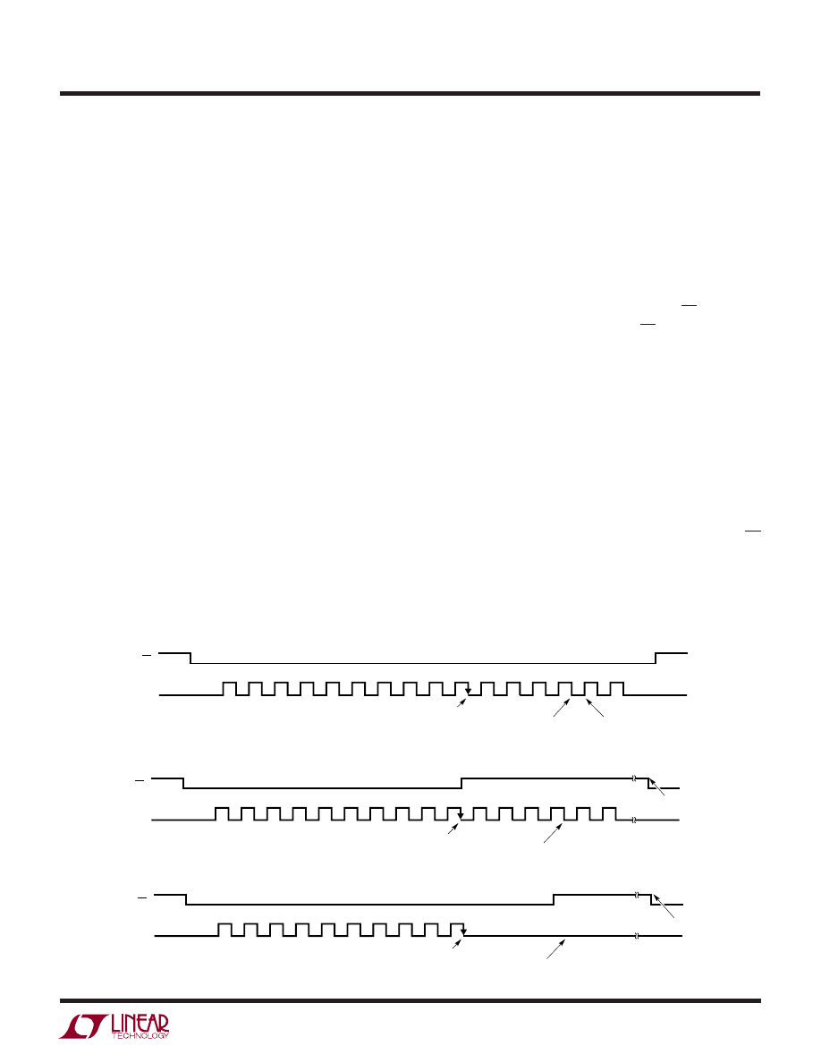
29
LTC1290
1290fe
U
S
A
O
PPLICATI
TYPICAL
Power Shutdown
For battery-powered applications it is desirable to keep
power dissipation at a minimum. The LTC1290 can be
powered down when not in use reducing the supply
current from a nominal value of 5mA to typically 5
µA (with
ACLK turned off). See the curve for Supply Current (Power
Shutdown) vs ACLK if ACLK cannot be turned off when the
LTC1290 is powered down. In this case the supply current
is proportional to the ACLK frequency and is independent
of temperature until it reaches the magnitude of the supply
current attained with ACLK turned off.
As an example of how to use this feature let’s add this to
the previous application, SNEAK-A-BIT. After the CHK
SIGN subroutine call insert the following:
•
•
JSR CHK SIGN
Determines which reading has valid
data, converts to 2’s complement
and stores in RAM
JSR SHUTDOWN
LTC1290 power shutdown routine
The actual subroutine is:
SHUTDOWN: LDA #$3D
Load D
IN
word for
LTC1290 into ACC
JSR TRANSFER Read LTC1290 routine
RTS
Return
To place the device in power shutdown the word length
bits are set to WL1 = 0 and WL0 = 1. The LTC1290 is
powered up on the next request for a conversion and it’s
ready to digitize an input signal immediately.
Power Shutdown Timing Considerations
After power shutdown has been requested, the LTC1290
is powered up on the next request for a conversion. This
request can be initiated either by bringing CS low or by
starting the next cycle of SCLKs if CS is kept low (see
Figures 3 and 4). When the SCLK frequency is much
slower than the ACLK frequency a situation can arise
where the LTC1290 could power down and then prema-
turely power back up. Power shutdown begins at the
negative going edge of the 10th SCLK once it has been
requested. A dummy conversion is executed and the
LTC1290 waits for the next request for conversion. If the
SCLKs have not finished once the LTC1290 has finished its
dummy conversion, it will recognize the next remaining
SCLKs as a request to start a conversion and power up the
LTC1290 (see Figure 23). To prevent this, bring either CS
high at the 10th SCLK (Figure 24) or clock out only 10
SCLKs (Figure 25) when power shutdown is requested.
1
10
SCLK
CS
POWER SHUTDOWN STARTS
DUMMY CONVERSION FINISHES AFTER 52 ACLK PERIODS
POWER UP
1290 TAF23
Figure 23. Power Shutdown Timing Problem
1
10
SCLK
CS
POWER SHUTDOWN STARTS
DUMMY CONVERSION FINISHES AFTER 52 ACLK PERIODS
POWER UP
1290 TAF24
Figure 24. Power Shutdown Timing
1
10
SCLK
CS
POWER SHUTDOWN STARTS
DUMMY CONVERSION FINISHES AFTER 52 ACLK PERIODS
POWER UP
1290 TAF25
Figure 25. Power Shutdown Timing
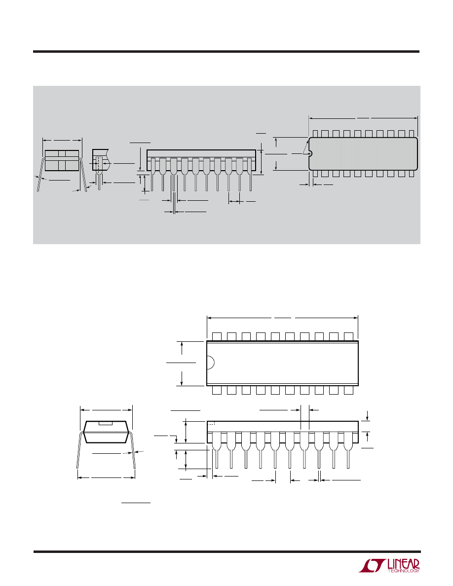
30
LTC1290
1290fe
J Package
20-Lead CERDIP (Narrow 0.300, Hermetic)
(LTC DWG # 05-08-1110)
OBSOLETE PACKAGE
J20 1298
3
7
5
6
10
9
1
4
2
8
11
20
16
15
17
14
13
12
19
18
0.005
(0.127)
MIN
0.025
(0.635)
RAD TYP
0.220 – 0.310
(5.588 – 7.874)
1.060
(26.924)
MAX
0
° – 15°
0.008 – 0.018
(0.203 – 0.457)
0.015 – 0.060
(0.381 – 1.524)
0.125
(3.175)
MIN
0.014 – 0.026
(0.356 – 0.660)
0.045 – 0.065
(1.143 – 1.651)
0.100
(2.54)
BSC
0.200
(5.080)
MAX
0.300 BSC
(0.762 BSC)
0.045 – 0.068
(1.143 – 1.727)
FULL LEAD
OPTION
0.023 – 0.045
(0.584 – 1.143)
HALF LEAD
OPTION
CORNER LEADS
OPTION
(4 PLCS)
NOTE: LEAD DIMENSIONS APPLY TO SOLDER
DIP/PLATE OR TIN PLATE LEADS
N Package
20-Lead PDIP (Narrow .300 Inch)
(Reference LTC DWG # 05-08-1510)
PACKAGE DESCRIPTIO
U
N20 0405
.020
(0.508)
MIN
.120
(3.048)
MIN
.125 – .145
(3.175 – 3.683)
.065
(1.651)
TYP
.045 – .065
(1.143 – 1.651)
.018
± .003
(0.457
± 0.076)
.005
(0.127)
MIN
.255
± .015*
(6.477
± 0.381)
1.060*
(26.924)
MAX
1
2
3
4
5
6
7
8
9
10
19
11
12
13
14
16
15
17
18
20
.008 – .015
(0.203 – 0.381)
.300 – .325
(7.620 – 8.255)
.325
+.035
–.015
+0.889
–0.381
8.255
(
)
NOTE:
1. DIMENSIONS ARE
INCHES
MILLIMETERS
*THESE DIMENSIONS DO NOT INCLUDE MOLD FLASH OR PROTRUSIONS.
MOLD FLASH OR PROTRUSIONS SHALL NOT EXCEED .010 INCH (0.254mm)
.100
(2.54)
BSC
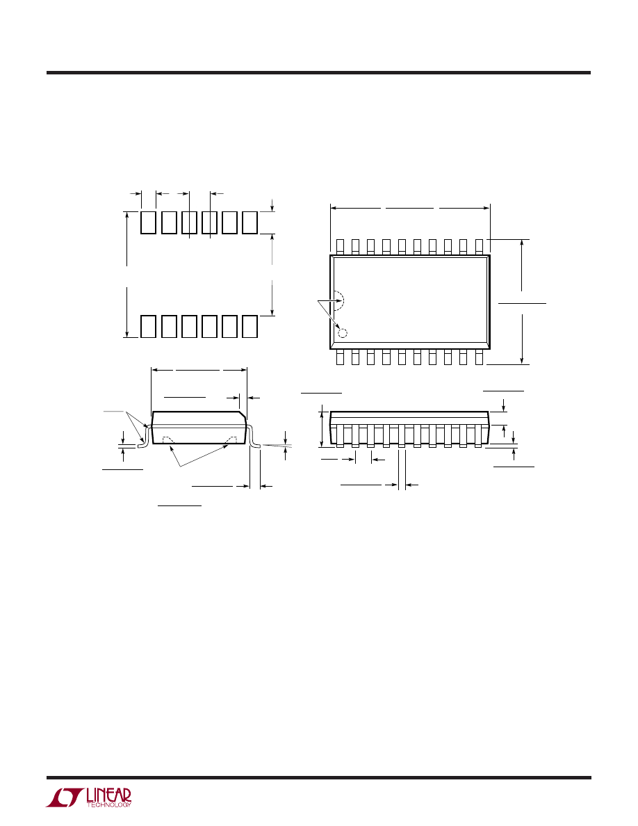
31
LTC1290
1290fe
SW Package
20-Lead Plastic Small Outline (Wide .300 Inch)
(Reference LTC DWG # 05-08-1620)
PACKAGE DESCRIPTIO
U
S20 (WIDE) 0502
NOTE 3
.496 – .512
(12.598 – 13.005)
NOTE 4
20
N
19
18
17
16
15
14
13
1
2
3
4
5
6
7
8
.394 – .419
(10.007 – 10.643)
9
10
N/2
11
12
.037 – .045
(0.940 – 1.143)
.004 – .012
(0.102 – 0.305)
.093 – .104
(2.362 – 2.642)
.050
(1.270)
BSC
.014 – .019
(0.356 – 0.482)
TYP
0
° – 8° TYP
NOTE 3
.009 – .013
(0.229 – 0.330)
.016 – .050
(0.406 – 1.270)
.291 – .299
(7.391 – 7.595)
NOTE 4
× 45°
.010 – .029
(0.254 – 0.737)
.420
MIN
.325
±.005
RECOMMENDED SOLDER PAD LAYOUT
.045
±.005
N
1
2
3
N/2
.050 BSC
.030
±.005
TYP
.005
(0.127)
RAD MIN
INCHES
(MILLIMETERS)
NOTE:
1. DIMENSIONS IN
2. DRAWING NOT TO SCALE
3. PIN 1 IDENT, NOTCH ON TOP AND CAVITIES ON THE BOTTOM OF PACKAGES ARE THE MANUFACTURING OPTIONS.
THE PART MAY BE SUPPLIED WITH OR WITHOUT ANY OF THE OPTIONS
4. THESE DIMENSIONS DO NOT INCLUDE MOLD FLASH OR PROTRUSIONS.
MOLD FLASH OR PROTRUSIONS SHALL NOT EXCEED .006" (0.15mm)
Information furnished by Linear Technology Corporation is believed to be accurate and reliable.
However, no responsibility is assumed for its use. Linear Technology Corporation makes no represen-
tation that the interconnection of circuits as described herein will not infringe on existing patent rights.

32
LTC1290
1290fe
LT/LT 0805 REV E • PRINTED IN USA
© LINEAR TECHNOLOGY CORPORATION 1991
Linear Technology Corporation
1630 McCarthy Blvd., Milpitas, CA 95035-7417
(408) 432-1900
●
FAX: (408) 434-0507
●
www.linear.com
PART NUMBER
DESCRIPTION
COMMENTS
LTC1286/LTC1298
12-Bit, Micropower Serial ADC in SO-8
1- or 2-Channel, Autoshutdown
LTC1293/LTC1294/LTC1296
12-Bit, Multiplexed Serial ADC
6-, 8- or 8-Channel with Shutdown Output
LTC1594/LTC1598
12-Bit, Micropower Serial ADC
4- or 8-Channel, 3V Versions Available
RELATED PARTS
Wyszukiwarka
Podobne podstrony:
Linear Technology Top Markings Nieznany
Linear Technology Top Markings Nieznany
LTC109x (Linear Technology)
LTC1090 (Linear Technology)
PORÓWNYWANIE TECHNOLOGII
19 Mikroinżynieria przestrzenna procesy technologiczne,
Technologia informacji i komunikacji w nowoczesnej szkole
Technologia spawania stali wysokostopowych 97 2003
SII 17 Technologie mobilne
W WO 2013 technologia
TECHNOLOGIA PŁYNNYCH POSTACI LEKU Zawiesiny
technologia prefabrykowana
Technology & Iventions
Technologia Maszyn CAD CAM
1 Infrastruktura, technika i technologia procesów logistyczid 8534 ppt
więcej podobnych podstron