HCC/HCF4089B
BINARY RATE MULTIPLIER
DESCRIPTION
.
CASCADABLE IN MULTIPLES OF 4-BITS
.
SET TO ”15” INPUT AND ”15” DETECT OUT-
PUT
.
QUIESCENT CURRENT SPECIFIED TO 20V
FOR HCC DEVICE
.
STANDARDIZED
SYMMETRICAL
OUTPUT
CHARACTERISTICS
.
INPUT CURRENT OF 100nA AT 18V AND
25
°
C FOR HCC DEVICE
.
100% TESTED FOR QUIESCENT CURRENT
.
MEETS ALL REQUIREMENTS OF JEDEC TEN-
TATIVE STANDARD N
o
. 13A, ”STANDARD
SPECIFICATIONS FOR DESCRIPTION OF ”B”
SERIES CMOS DEVICES”
June 1989
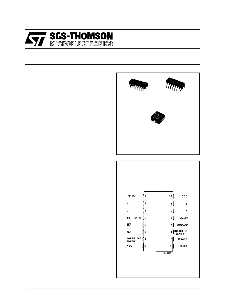
The HCC4089B (extended temperature range) and
HCF4089B (intermediate temperature range) are
monolithic integrated circuit available in 16-lead
dual in-line plastic or ceramic package.
The HCC/HCF4089B is a low-power 4-bit digital
rate multiplier that provides an output pulse rate that
is the clock-input-pulse rate multiplied by 1/16 times
the binary input. For example, when the binary input
number is 13, there will be 13 output pulses for every
16 input pulses.
The HCC/HCF4089B has an internal synchronous
4-bit counter which, together with one of the four bi-
nary input bits, produces pulse trains as shown in
timing diagram.
If more than one binary input bit is high, the resulting
pulse train is a combination of the above separate
pulse trains. This device may be used to perform
arithmetic operations (add, subtract, divide, raise to
a power), solve algebraic and differential equations,
generate natural logarithms and trigonometric func-
tions, A/D and D/A conversions, and frequency di-
vision.
EY
(Plastic Package)
F
(Ceramic Package)
C1
(Chip Carrier)
ORDER CODES :
HCC4089BF
HCF4089BEY
HCF4089BC1
PIN CONNECTIONS
1/13
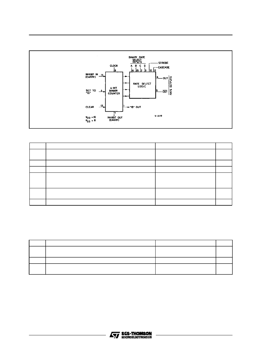
FUNCTIONAL DIAGRAM
ABSOLUTE MAXIMUM RATINGS
Symbol
Parameter
Value
Unit
V
DD
*
Supply Voltage : H CC Types
H C F Types
– 0.5 to + 20
– 0.5 to + 18
V
V
V
i
Input Voltage
– 0.5 to V
DD
+ 0.5
V
I
I
DC Input Current (any one input)
±
10
mA
P
t o t
Total Power Dissipation (per package)
Dissipation per Output Transistor
for T
o p
= Full Package-temperature Range
200
100
mW
mW
T
o p
Operating Temperature : HCC Types
H CF Types
– 55 to + 125
– 40 to + 85
°
C
°
C
T
st g
Storage Temperature
– 65 to + 150
°
C
RECOMMENDED OPERATING CONDITIONS
Symbol
Parameter
Value
Unit
V
DD
Supply Voltage : HC C Types
H CF Types
3 to 18
3 to 15
V
V
V
I
Input Voltage
0 to V
DD
V
T
o p
Operating Temperature : HCC Types
H CF Types
– 55 to + 125
– 40 to + 85
°
C
°
C
Stresses above those listed under ”Absolute Maximum Ratings” may cause permanent damage to the device. This is a stress rating only and
functional operation of the device at these or any other conditions above those indicated in the operational sections of this specification is not implied.
Exposure to absolute maximum rating conditions for external periods may affect device reliability.
* All voltage values are referred to V
SS
pin voltage.
HCC/HCF4089B
2/13
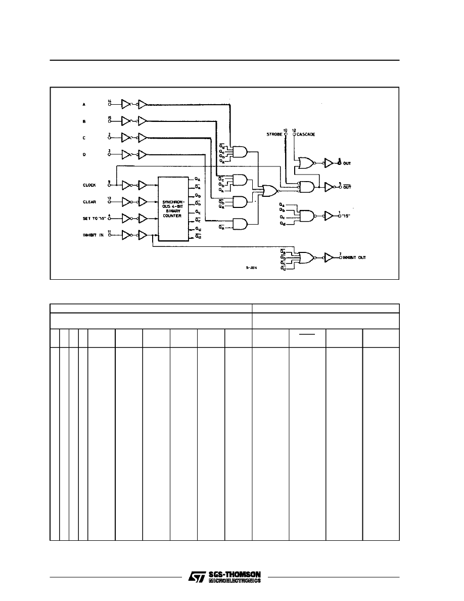
LOGIC DIAGRAM
TRUTH TABLE
Inputs
Outputs
Number of Pulses or I nput Logic Level
(0 = low ; 1 = high ; X = don’t care)
Number of Pulses or Output Logic Level
(L = low ; H = high)
D C B A
CLK
I N H
I N
ST R
CAS
CLR
S ET
O U T
O U T
I NH
O U T
”15”
O U T
0
0
0
0
0
0
0
0
1
1
1
1
1
1
1
1
X
X
X
1
0
X
0
0
0
0
1
1
1
1
0
0
0
0
1
1
1
1
X
X
X
X
X
X
0
0
1
1
0
0
1
1
0
0
1
1
0
0
1
1
X
X
X
X
X
X
0
1
0
1
0
1
0
1
0
1
0
1
0
1
0
1
X
X
X
X
X
X
16
16
16
16
16
16
16
16
16
16
16
16
16
16
16
16
16
16
16
16
16
16
0
0
0
0
0
0
0
0
0
0
0
0
0
0
0
0
1
0
0
0
0
0
0
0
0
0
0
0
0
0
0
0
0
0
0
0
0
0
0
1
0
0
0
0
0
0
0
0
0
0
0
0
0
0
0
0
0
0
0
0
0
0
1
0
0
0
0
0
0
0
0
0
0
0
0
0
0
0
0
0
0
0
0
0
0
1
1
0
0
0
0
0
0
0
0
0
0
0
0
0
0
0
0
0
0
0
0
0
0
1
L
1
2
3
4
5
6
7
8
9
10
11
12
13
14
15
•
L
H
16
L
L
H
1
2
3
4
5
6
7
8
9
10
11
12
13
14
15
•
H
*
16
H
H
1
1
1
1
1
1
1
1
1
1
1
1
1
1
1
1
H
1
1
H
H
L
1
1
1
1
1
1
1
1
1
1
1
1
1
1
1
1
•
1
1
L
L
H
* Output same as the first 16 lines of this truth table (depending on values of A, B, C, D).
•
Depends on internal state of counter.
HCC/HCF4089B
3/13
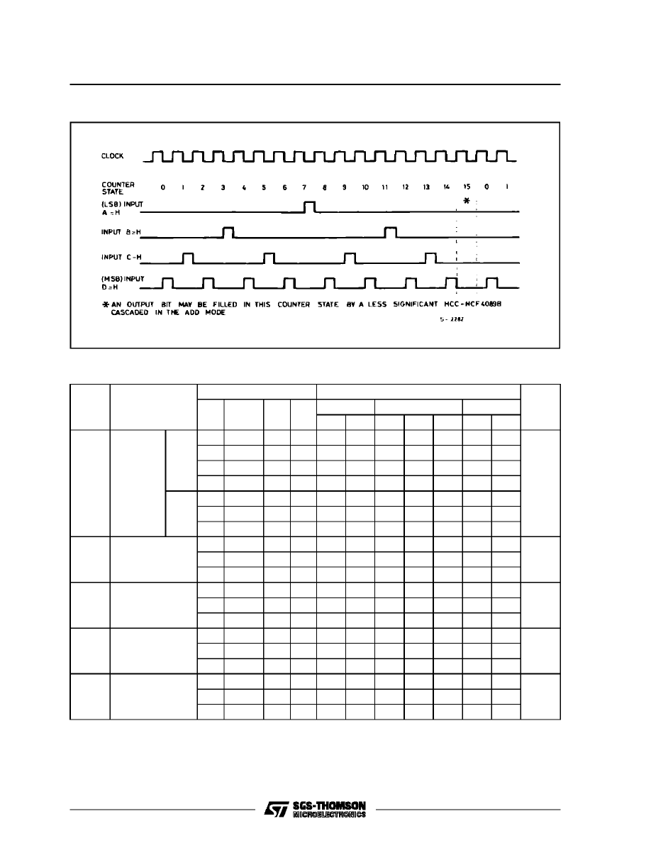
TIMING DIAGRAM
STATIC ELECTRICAL CHARACTERISTICS (over recommended operating conditions)
Test Conditions
Value
V
I
V
O
|I
O
|
V
D D
T
L o w
*
25
°
C
T
Hi g h
*
Symbol
Parameter
(V)
(V)
(
µ
A)
(V)
Min. Max. Min. Typ. Max. Min. Max.
Unit
I
L
Quiescent
Current
HCC
Types
0/ 5
5
5
0.04
5
150
µ
A
0/10
10
10
0.04
10
300
0/15
15
20
0.04
20
600
0/20
20
100
0.08
100
3000
HCF
Types
0/ 5
5
20
0.04
20
150
0/10
10
40
0.04
40
300
0/15
15
80
0.04
80
600
V
O H
Output High
Voltage
0/ 5
< 1
5
4.95
4.95
4.95
V
0/10
< 1
10
9.95
9.95
9.95
0/15
< 1
15
14.95
14.95
14.95
V
O L
Output Low
Voltage
5/0
< 1
5
0.05
0.05
0.05
V
10/0
< 1
10
0.05
0.05
0.05
15/0
< 1
15
0.05
0.05
0.05
V
IH
Input High
Voltage
0.5/4.5
< 1
5
3.5
3.5
3.5
V
1/9
< 1
10
7
7
7
1.5/13.5
< 1
15
11
11
11
V
IL
Input Low
Voltage
4.5/0.5
< 1
5
1.5
1.5
1.5
V
9/1
< 1
10
3
3
3
13.5/1.5
< 1
15
4
4
* T
Low
= – 55
°
C for HCC device : – 40
°
C for HCF device.
* T
High
= + 125
°
C for HCC device : + 85
°
C for HCF device.
The Noise Margin for both ”1” and ”0” level is : 1V min. with V
DD
= 5V, 2V min. with V
DD
= 10V, 2.5V min. with V
DD
= 15V.
HCC/HCF4089B
4/13
* T
Low
= – 55
°
C for HCC device : – 40
°
C for HCF device.
* T
High
= + 125
°
C for HCC device : + 85
°
C for HCF device.
The Noise Margin for both ”1” and ”0” level is : 1V min. with V
DD
= 5V, 2V min. with V
DD
= 10V, 2.5V min. with V
DD
= 15V.
STATIC ELECTRICAL CHARACTERISTICS (continued)
Test Conditions
Value
V
I
V
O
|I
O
|
V
D D
T
L o w
*
25
°
C
T
Hi g h
*
Symbol
Parameter
(V)
(V)
(
µ
A)
(V)
Min. Max. Min. Typ. Max. Min. Max.
Unit
I
O H
Output
Drive
Current
HCC
Types
0/ 5
2.5
5
– 2
– 1.6 – 3.2
– 1.15
mA
0/ 5
4.6
5
– 0.64
– 0.51 – 1
– 0.36
0/10
9.5
10
– 1.6
– 1.3 – 2.6
– 0.9
0/15
13.5
15
– 4.2
– 3.4 – 6.8
– 2.4
HCF
Types
0/ 5
2.5
5
– 1.53
– 1.36 – 3.2
– 1.1
0/ 5
4.6
5
– 0.52
– 0.44 – 1
– 0.36
0/10
9.5
10
– 1.3
– 1.1 – 2.6
– 0.9
0/15
13.5
15
– 3.6
– 3.0 – 6.8
– 2.4
I
O L
Output
Sink
Current
HCC
Types
0/ 5
0.4
5
0.64
0.51
1
0.36
mA
0/10
0.5
10
1.6
1.3
2.6
0.9
0/15
1.5
15
4.2
3.4
6.8
2.4
HCF
Types
0/ 5
0.4
5
0.52
0.44
1
0.36
0/10
0.5
10
1.3
1.1
2.6
0.9
0/15
1.5
15
3.6
3.0
6.8
2.4
I
IH
, I
IL
Input
Leakage
Current
HCC
Types
0/18
Any Input
18
±
0.1
±
10
– 5
±
0.1
±
1
µ
A
HCF
Types
0/15
15
±
0.3
±
10
– 5
±
0.3
±
1
C
I
Input Capacitance
Any Input
5
7.5
pF
HCC/HCF4089B
5/13
DYNAMIC ELECTRICAL CHARACTERISTICS (T
amb
= 25
°
C, C
L
= 50pF, R
L
= 200k
Ω
,
typical temperature coefficient for all V
DD
values is 0.3%/
°
C, all input rise and fall times = 20ns)
Test Conditions
Val ue
Symbol
Parameter
V
D D
(V)
Min.
Typ.
Max.
Uni t
t
PHL
, t
PL H
Propagation
Delay Time
Clock to out
5
110
220
ns
10
55
110
15
45
90
Clock or Strobe to
out
5
150
300
ns
10
75
150
15
60
120
Clock to Inhibit
High Level to Low
Level
5
360
720
ns
10
160
320
15
110
220
Low Level to High
Level
5
250
500
ns
10
100
200
15
75
150
Clear to out
5
380
760
ns
10
175
350
15
130
260
Clock to ”9” or
”15” out
5
300
600
ns
10
125
250
15
90
180
Cascade to out
5
90
180
ns
10
45
90
15
35
70
Inhibit in to Inhibit
out
5
160
320
ns
10
75
150
15
55
110
Set to out
5
330
660
ns
10
150
300
15
110
220
HCC/HCF4089B
6/13
DYNAMIC ELECTRICAL CHARACTERISTICS (continued )
Test Conditions
Val ue
Symbol
Parameter
V
D D
(V)
Min.
Typ.
Max.
Unit
t
THL
, t
T L H
Transition Time
5
100
200
ns
10
50
100
15
40
80
f
CL
Maximum Clock Frequency
5
1.2
2.4
MHz
10
2.5
5
15
3.5
7
t
W
Clock Pulse Width
5
330
165
ns
10
170
85
15
100
50
t
r
, t
f
Clock Rise or Fall Time
5
15
µ
s
10
15
15
15
t
W
Set or Clear Pulse Width
5
160
80
ns
10
90
45
15
60
30
t
se t u p
Inhibit Input Setup Time, High
Level to Low Level
5
100
50
ns
10
40
20
15
20
10
t
R
Inhibit, Input Removal Time
5
240
120
ns
10
130
65
15
110
55
t
R
Minimum Set Removal Time
5
150
75
ns
10
80
40
15
50
25
t
R
Clear Removal Time
5
60
30
ns
10
40
20
15
30
15
HCC/HCF4089B
7/13
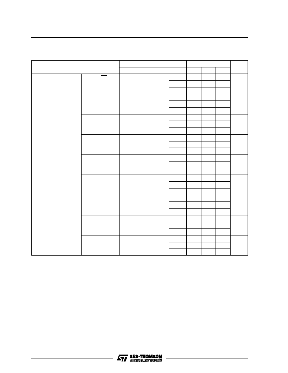
A
B
1
N
When the loop stabilies rate R2 = rate R3, thus fclock (
.
) = fclock (
.
) therefore N = A.B.
16 16
16 16
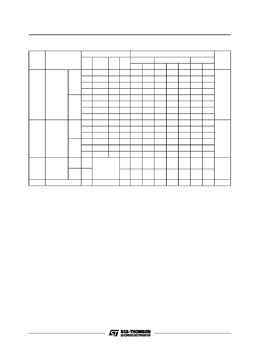
APPLICATION NOTES
For words of more than 4 bits, HCC/HCF4089B devices may be cascaded in two different modes : an Add
mode and a Multiply mode.
Two HCC/HCF4089B’s cascaded in the ”Add” mode with a preset number of 189.
Nota :
In the Add mode some of the gaps left by the more
significant unit at the count of 15 are filled in by the
less significant units. For example, when two units
are cascaded in the Add mode and programmed to
11 and 13, respectively, the more significant unit will
have 11 output pulses for every 16 input pulses and
the other unit will have 13 output pulses for every
256 input pulses for a total of
11
13
189
+
=
16
256
256
Two HCC/HCF4089B’s cascaded in the Multiply mode for Multiplication of two variables A and B with loop
circuit control.
HCC/HCF4089B
8/13
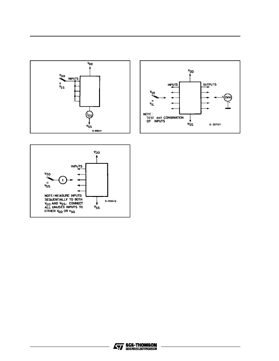
Input Leakage Current.
Noise Immunity.
TEST CIRCUITS
Quiescent Device Current.
HCC/HCF4089B
9/13
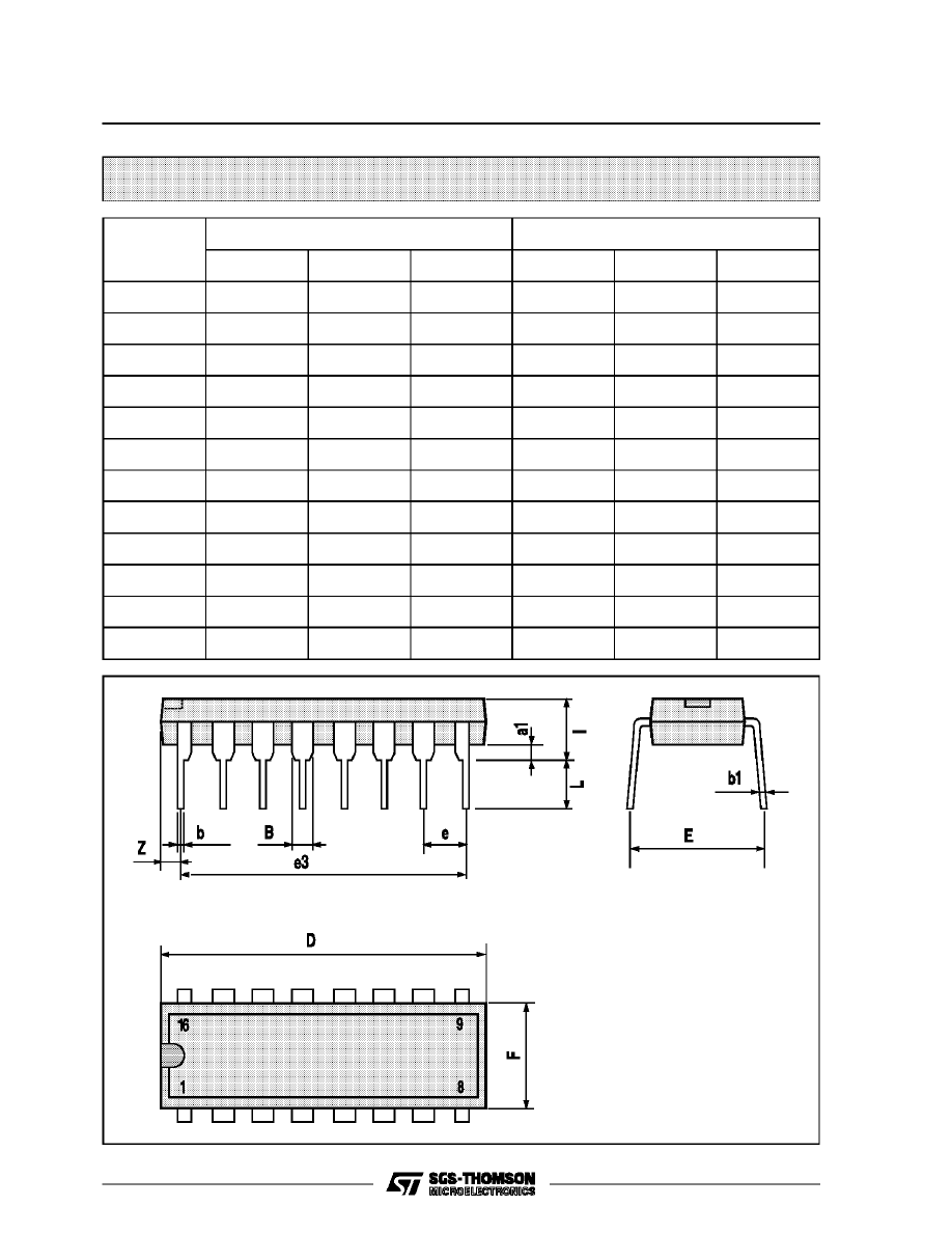
Plastic DIP16 (0.25) MECHANICAL DATA
DIM.
mm
inch
MIN.
TYP.
MAX.
MIN.
TYP.
MAX.
a1
0.51
0.020
B
0.77
1.65
0.030
0.065
b
0.5
0.020
b1
0.25
0.010
D
20
0.787
E
8.5
0.335
e
2.54
0.100
e3
17.78
0.700
F
7.1
0.280
I
5.1
0.201
L
3.3
0.130
Z
1.27
0.050
P001C
HCC/HCF4089B
10/13
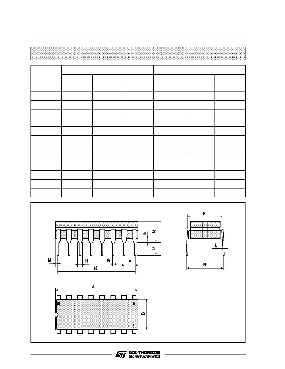
Ceramic DIP16/1 MECHANICAL DATA
DIM.
mm
inch
MIN.
TYP.
MAX.
MIN.
TYP.
MAX.
A
20
0.787
B
7
0.276
D
3.3
0.130
E
0.38
0.015
e3
17.78
0.700
F
2.29
2.79
0.090
0.110
G
0.4
0.55
0.016
0.022
H
1.17
1.52
0.046
0.060
L
0.22
0.31
0.009
0.012
M
0.51
1.27
0.020
0.050
N
10.3
0.406
P
7.8
8.05
0.307
0.317
Q
5.08
0.200
P053D
HCC/HCF4089B
11/13
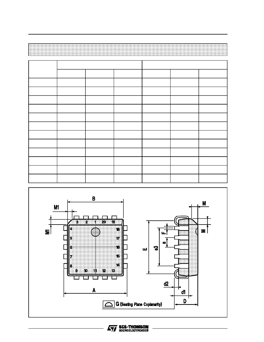
PLCC20 MECHANICAL DATA
DIM.
mm
inch
MIN.
TYP.
MAX.
MIN.
TYP.
MAX.
A
9.78
10.03
0.385
0.395
B
8.89
9.04
0.350
0.356
D
4.2
4.57
0.165
0.180
d1
2.54
0.100
d2
0.56
0.022
E
7.37
8.38
0.290
0.330
e
1.27
0.050
e3
5.08
0.200
F
0.38
0.015
G
0.101
0.004
M
1.27
0.050
M1
1.14
0.045
P027A
HCC/HCF4089B
12/13

Information furnished is believed to be accurate and reliable. However, SGS-THOMSON Microelectronics assumes no responsability for the
consequences of use of such information nor for any infringement of patents or other rights of third parties which may results from its use. No
license is granted by implication or otherwise under any patent or patent rights of SGS-THOMSON Microelectronics. Specifications mentioned
in this publication are subject to change without notice. This publication supersedes and replaces all information previously supplied.
SGS-THOMSON Microelectronics products are not authorized for use as critical components in life support devices or systems without express
written approval of SGS-THOMSON Microelectonics.
1994 SGS-THOMSON Microelectronics - All Rights Reserved
SGS-THOMSON Microelectronics GROUP OF COMPANIES
Australia - Brazil - France - Germany - Hong Kong - Italy - Japan - Korea - Malaysia - Malta - Morocco - The Netherlands -
Singapore - Spain - Sweden - Switzerland - Taiwan - Thailand - United Kingdom - U.S.A
HCC/HCF4089B
13/13
Wyszukiwarka
Podobne podstrony:
4089
4089
4089
4089
4089
4089
4089
4089
4089 12572 2 PB
więcej podobnych podstron