1
Calculation of PCB Track Impedance
by
Andrew J Burkhardt, Christopher S Gregg and J Alan Staniforth
INTRODUCTION
The use of high-speed circuits requires PCB tracks to be
designed with controlled (characteristic, odd-mode, or
differential) impedances. Wadell
[1]
is one of the most
comprehensive sources of equations for evaluating these
impedances. This source includes many configurations
including stripline, surface microstrip, and their coplanar
variants.
The IPC publication, IPC-2141
[2]
, is another source of
equations but has a smaller range of configurations, similar
to those presented in IPC-D-317A.
However, for some configurations there are differences
between the equations given in
these publications. The
authors believe that it is now opportune to examine the
origin of the equations and to update the method of
calculation for use with modern personal computers.
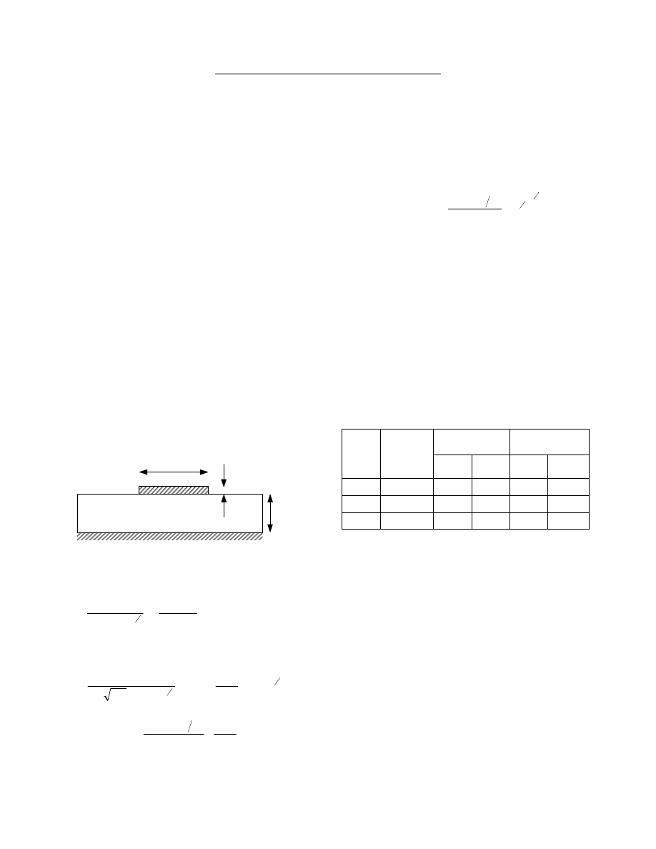
As an example, consider the surface microstrip shown in
Figure 1.
Figure 1 - Surface Microstrip
IPC-2141
[2]
gives the characteristic impedance as
(
)
+
+
=
t
w
Z
r
8
.
0
98h
.
5
ln
41
.
1
0
.
87
2
1
0
ε
(1)
Wadell
[1]
gives
(
)
(
)
+
+
+
=
2
1
2
1
'
0
.
4
0
.
1
ln
1
0
.
2
0
.
2
0
0
B
A
w
h
Z
r
ε
π
η
(2)
where
'
0
.
4
0
.
11
0
.
8
0
.
14
w
h
A
r
×
+
=
ε
(3a)
2
1
2
1
0
.
2
0
.
1
0
.
1
2
×
+
+
=
π
ε
r
A
B
(3b)
with
'
'
w
w
w
∆
+
=
(3c)
The parameter w' is the equivalent width of a track of zero
thickness due to a track of rectangular profile, width w and
thickness t. Wadell
[1]
gives an additional equation to
determine the incremental value
∆
w'. The parameter
η
o
, in
equation (2), is the impedance of free-space (or vacuum),
376.7
Ω
(
≈
120
π
). The quoted accuracy is 2% for any value
of
ε
r
and w.
Table 1 shows the results of applying equations (1) and (2)
to a popular surface microstrip constructed from 1oz copper
track on
1
/
32
inch substrate.
Table 1
Equation
(1)
Equation
(2)
Width
w
(
µ
m)
Numerical
Method
Z
0
(
Ω
)
Z
0
(
Ω
)
% error
Z
0
(
Ω
)
% error
3300
30.09
21.08
-29.94
29.89
-0.66
1500
50.63
49.46
-2.31
50.50
-0.26
450
89.63
91.79
+2.41
89.89
+0.29
t = 35
µ
m, h = 794
µ
m,
ε
r
= 4.2
(the calculation of the error assumes the numerical method
is accurate : see Numerical Results)
Table 1 shows that equation (2) is well within the quoted
accuracy. The accuracy of equation (1) varies widely, but
this equation has the advantage of simplicity and is useful in
illustrating the general changes to the value of Z
0
as the
width w and thickness t are varied.
The example demonstrated by Table 1, highlights the
general problem with published equations: complicated
equations are usually more accurate. Ranges over which the
equations are accurate are also usually restricted to a limited
range of parameters (e.g. w/h, t/h and
ε
r
).
Equation (2) is complicated, but with patience, can be
evaluated using a programmable calculator or computer
Substrate
Dielectric constant
ε
r
w
h
t

2
spreadsheet. However the complications increase greatly
when two coupled tracks are used to give a differential
impedance. For coupled surface microstrip, Wadell
[1]
gives
7 pages of equations to evaluate the impedance.
It is now a major exercise to evaluate the impedance using a
calculator or spreadsheet.
ALGEBRAIC EQUATIONS
Single Track
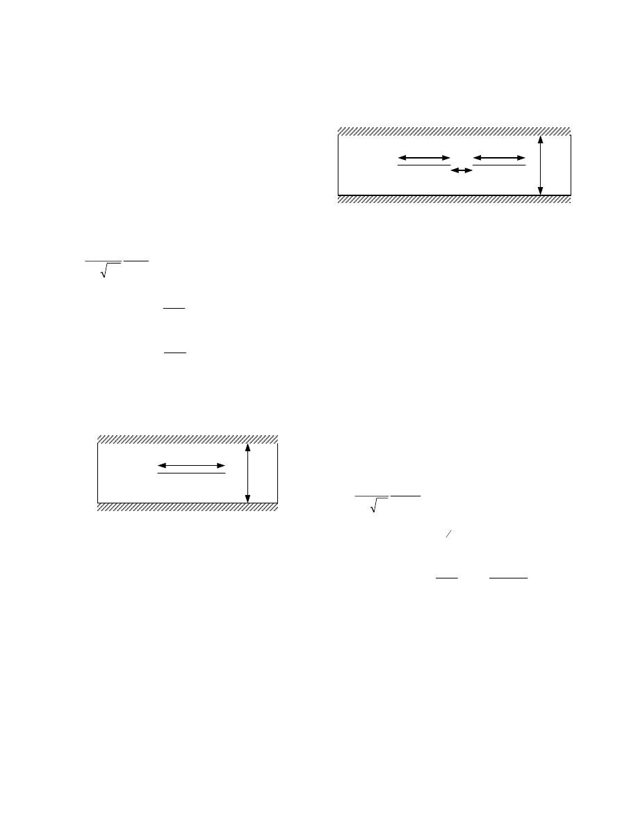
For the stripline of Figure 2 with a symmetrically centred
track of zero thickness, Cohn
[3]
has shown that the exact
value of the characteristic impedance is
( )
( )
'
0
.
4
0
0
k
K
k
K
E
Z
r
η
=
(4)
where
=
h
w
k
0
.
2
sech
π
(5a)
and
=
h
w
k
0
.
2
tanh
'
π
(5b)
K is the complete elliptic function of the first kind
[4]
. An
equation for the evaluation of the ratio of the elliptic
functions, accurate to 10
-12
, has been given by Hilberg
[5]
,
and also quoted by Wadell
[1]
.
Figure 2 - Stripline: Centred Track
When the thickness is not zero, corrections have to be made
which are approximate
[1]
. These corrections are obtained
from theoretical approximations or curve fitting the results
of numerical calculations based on the fundamental
electromagnetic field equations.
When the track is offset from the centre, the published
equations become more complicated and the range of
validity, for a given accuracy, is reduced.
Attempts have also been made to include the effects of
differential etching on the track resulting in a track cross-
section which is trapezoidal
[1]
.
There is no closed-form equation like equation (4) for
surface or embedded microstrip of any track thickness.
Thus any equation used to calculate the impedance is
approximate and demonstrated in Table 1.
Coupled Coplanar Tracks
Figure 3 shows two coupled coplanar centred stripline
tracks.
Figure 3 - Stripline : Coplanar
Coupled Centred Tracks
All the impedance equations for coupled configurations
refer to both even-mode impedance (Z
0e
) and odd-mode
impedance (Z
0o
). These impedances are measured between
the tracks and the ground plane. Z
0e
occurs when tracks A
and B are both at +V relative to the ground plane, and Z
0o
occurs when track A is at +V and track B is at –V. When a
differential signal is applied between A and B, then a
voltage exists between the tracks similar to the odd-mode
configuration. The impedance presented to this signal is
then the differential impedance,
o
diff
Z
Z
0
2
×
=
(6)
All published equations [1] give Z
0o
. The differential
impedance must then be obtained using equation (6).
For the zero thickness configuration of Figure 3, Cohn
[3]
gives the exact expression.
( )
( )
0
0
0
0
'
0
.
4
k
K
k
K
Z
r
o
ε
η
=
(7)
where
(
)
2
1
2
0
0
'
1 k
k
−
=
(8a)
and
(
)
+
=
h
s
w
h
w
k
0
.
2
coth
0
.
2
tanh
'
0
π
π
(8b)
As before K is the elliptic function of the first kind. There
are no closed-form equations for coplanar coupled tracks.
Effect of Track Thickness
When the track thickness is not zero, approximations must
be made to obtain algebraic equations similar to equations
(4) and (7). Alternatively, equations, based on curve fitting
of extensive numerical calculations, are used.
However, as the thickness increases the impedance
decrease, as can be noted from equation (1).
Substrate
ε
r
w
h
w
s
B
A
Substrate
ε
r
w
h

3
NUMERICAL PRINCIPLES
For pulses on a uniform transmission system,
[1,6]
then
(
)
C
L
Z
or
Z
o
=
0
0
(9)
where L is the inductance and C the capacitance per unit
length of line.
For a stripline, where the electric (and magnetic) fields are
in a uniform substrate, dielectric constant
ε
r
, equation (9)
becomes
cC
Z
r
ε
=
0
(10)
where c is the velocity of light in vacuuo (or free-space).
The velocity of pulse travel along the transmission path is
r
c
ε
ν =
(11)
For a microstrip, the electric (and magnetic) fields are in air
and the substrate, It can be shown that
air
CC
c
Z
1
0
=
(12)
Where C
air
is the capacitance of the same track
configuration without substrate. The effective dielectric
constant is
air
eff
C
C
=
ε
(13)
To find the impedance, the capacitance must be calculated.
This can be done by applying a voltage V to the tracks and
calculating the total charge per unit length Q, from which
V
Q
C
=
(14)
However the surface charge on a track is not uniform. In
fact it is very high at track corners. Therefore the total
charge is difficult to calculate.
From electrostatic theory, it is known that a charge produces
a voltage at a distance r from the charge. Then a
distribution of charge
ρ
(coulomb/unit width of track) gives
a voltage
∫
=
l
G
V
ρδ
(15)
where the integral is taken over the perimeter of the track
cross-section,
δ
l is a small length, and G is the voltage due
to a unit charge. It is also known as the Green’s Function.
The value of G depends on the configuration (or
environment). For instance, a point charge in a 2
dimensional dielectric space, without conductors gives
( )
r
r
V
ε
πε
ρ
0
2
ln
−
=
(16a)
so that
( )
r
r
G
ε
πε
0
2
ln
−
=
(16b)
In equation (15), the voltage V is known, G is known for the
particular configuration of tracks and substrate, but the
charge
ρ
is unknown. Thus (15) is an integral equation
which can be solved numerically by the Method of
Moments (MoM)
[7]
.
To proceed using MoM, the cross-section perimeter of the
track is divided into short lengths with a node at each end.
Charges are assigned to each node. The voltage at each
node is calculated from all the nodal charges and the
estimated charge variation between nodes. This leads to a
set of simultaneous equations represented by the matrix
equation
V
A
=
ρρρρ
(17)
where
ρρρρ
is a vector of nodal charges, and V is a vector of
nodal voltages. A is a square matrix whose elements are
calculated from integrals involving the Green’s Function.
The size of the matrices depends on the number of nodes.
Equation (17) can be solved for the nodal charges
ρρρρ
for
given nodal voltages V. The elements of V are usually +1
or –1 depending on the configuration.
The total charge Q can be obtained by a suitable summation
of the nodal charges.
This general approach has been used by most authors to
evaluate the various impedances. Most of the calculations
were published 15 to 20 years ago, when the principal
calculator was a main-frame computer. Hence the need for
equations which could be used with the pocket calculators
available at that time.

4
The present authors have revisited the basic numerical
approach and have developed software
[8]
which readily
calculates the controlled impedances using a desktop PC.
The software runs quickly on a modern PC, and has been
extended to also include the calculation of configurations
not well represented in the literature. This includes
•
offset coupled stripline,
•
broadside coupled stripline,
•
embedded coupled microstrip.
Thick tracks are normally to be expected which have a
trapezoidal cross-section to allow for differential etching of
the track.
NUMERICAL RESULTS
This section describes in more detail some of the numerical
techniques and compares the results with the exact
equations (4) and (7).
In all cases the Green’s Function for the configurations was
obtained using charge images in the ground planes. There
are an infinite number of these images. In the case of
stripline the sum of images converges to the result given by
Sadiku
[9]
. Silvester
[10,11]
developed the image method for
surface microstrip and has now been extended by the
authors for embedded microstrip. In all cases the sum of
images converges, but the result has to be obtained
numerically.
The distribution of charge over an element between nodes is
assumed to be linear. A numerical singularity occurs when
the charge node j coincides with the voltage node i.
Sadiku
[9]
indicated how this can be resolved. The
evaluation of the elements A
ij
consists of both numerical and
analytic integration in the same manner as that used in
Boundary Element techniques
[12,13]
.
To avoid numerical inaccuracies at corners where there is a
large concentration of charge, the length of an element at a
corner is made very small. The other elements and nodes
are then distributed by the method described by
Kobayashi
[14]
. This means that wide strips require more
nodes than narrow strips when the same small element is
used.
The results presented were performed on a PC with an Intel
Pentium Pro running at 233MHz using a compiled C-
program.
Single Track Stripline
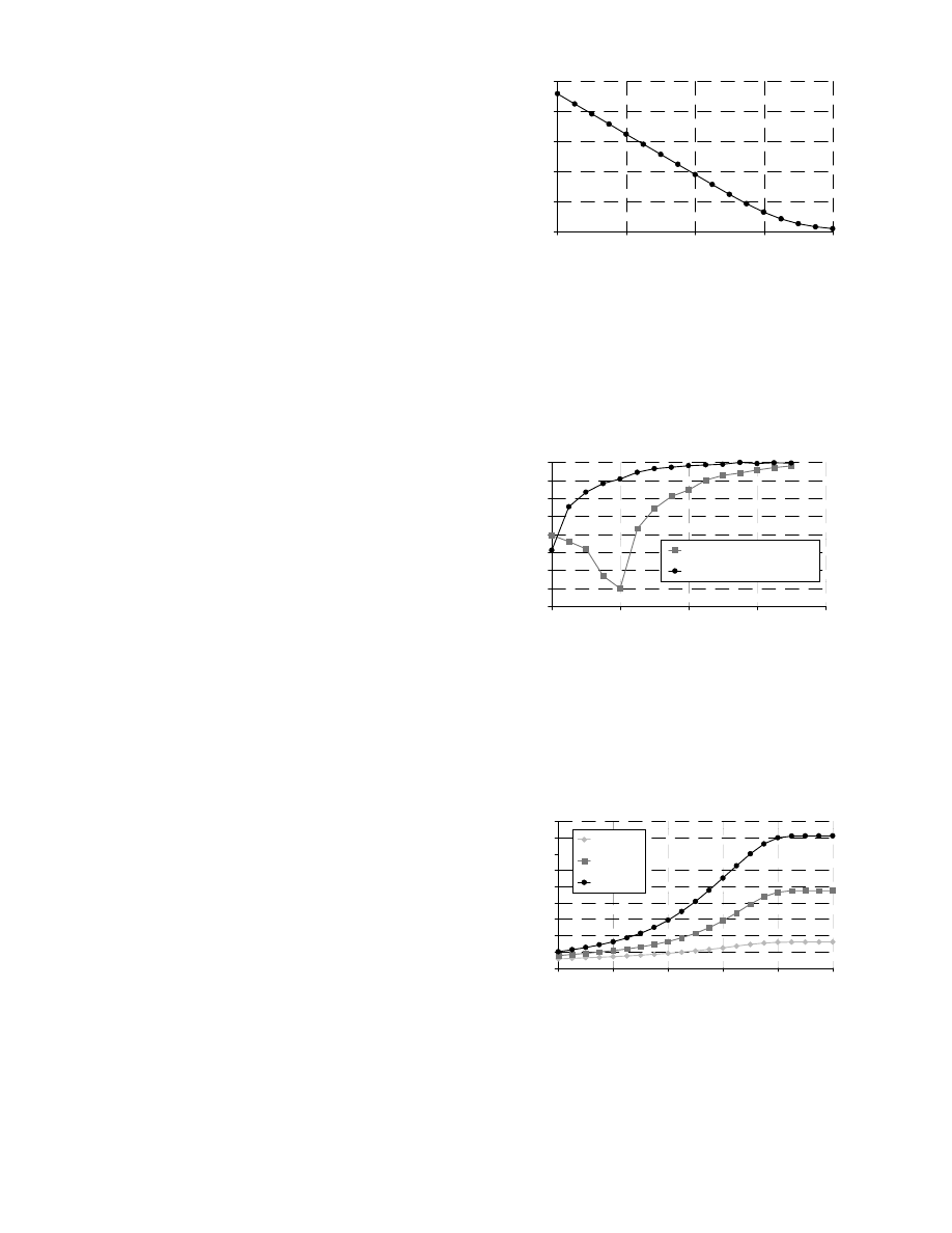
Figure 4 shows the variation of impedance with track width
for the stripline of Figure 2.
Figure 4 - Impedance for different relative width
(Substrate
εεεε
r
= 4.2)
Figure 5 shows the % error of the numerical calculation
compared with the exact values given by equation (4). Two
curves are shown for different small elements at the corner
(i.e. ends of the track).
Figure 5 - Substrate
εεεε
r
= 4.2
The above graph shows that good accuracy can be obtained
over nearly four decades of the width/height ratio. The
computer processing time was less than 0.5s for any of
these values.
Figure 6 - Odd-mode impedance for different
separations
(
s
/
h
)
and widths
(
w
/
h
)
0
50
100
150
200
250
1.00E-03
1.00E-02
1.00E-01
1.00E+00
1.00E+01
w/h
Z
0
(
Ω
Ω
Ω
Ω
)
-16
-14
-12
-10
-8
-6
-4
-2
0
1.00E-03
1.00E-02
1.00E-01
1.00E+00
1.00E+01
w/h
% Error (x10
-2
)
Smallest Element = 10-3
Smallest Element = 10-4
0
20
40
60
80
100
120
140
160
180
0.0001
0.001
0.01
0.1
1
10
s/h
Z
0o
(
ΩΩΩΩ
)
w/h=1.0
w/h=0.1
w/h=0.01

5
Coupled Coplanar Stripline
Figure 6 shows the variation of the odd-mode impedance
for the stripline shown in Figure 3.
Figure 7 - % error
εεεε
r
= 4.2
Figure 7 shows the % error of the numerical calculation
compared with the exact values given by equation (7) using
10
-3
as the smallest element. The maximum processing time
was less then 0.5s. The maximum error can be reduced by
decreasing the smallest element. For a maximum error of
6.0x10
-2
%, a processing time of 5.1s is required.
The results presented in Figure 7 offer a very stringent test
for the numerical method because of the sharp corners
separated by s. In the odd-mode configuration this effect is
enhanced even more because the tracks are of opposite
polarity. This numerical validation is considered to be
better then the results given by Bogatin et. al.
[15]
for a pair
of ‘round’ tracks (i.e. a parallel wire transmission line)
using finite element software. In this latter case there are no
singularities at the corners. Li and Fujii
[16]
state that the
boundary element method (to which MoM is related) is
more accurate for stripline and microstrip than the finite
element method.
Surface Microstrip
As previously mentioned there are no closed-form algebraic
equations which are exact. But the discussion in the
previous sections shows that the software can be made
accurate, especially for practical purposes. Table 1 shows
calculations for the configuration of Figure 1. Because the
Green’s Function involves a summation, and two
capacitances C and C
air
are required, processing times are
now longer than those for stripline. The longest time was
less than 4.5s for a width of 3300
µ
m.
For coupled surface microstrip, two thick tracks of 3300
µ
m
requires a processing time of 5.1s. The separation does not
affect the time.
PRACTICAL RESULTS
In order to verify the practical performance of the field
solving boundary element method, the authors
commissioned production of a set of samples. During a six
month period in 1998, over 1500 different printed circuit
board tracks were manufactured.
This sample consisted of both stripline and microstrip
differential structures in surface and embedded
configurations. Two types of coupled structures were
included; edge-coupled and boardside-coupled. The track
dimensions ranged from 75
µ
m to 1000
µ
m in width, with
differential separations of 1 track width to 4 track widths
using base copper weights of ½oz, 1oz and 2oz. The
resulting differential impedances ranged from 80
Ω
to 200
Ω
.
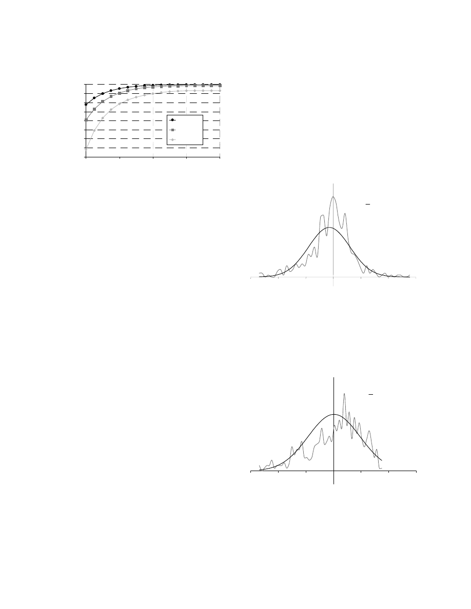
Figure 8 - Distribution of differences between predicted
and measured values for stripline
Test samples were produced by three independent UK
printed circuit board manufacturers
[17]
and the differential
impedances were electrically measured by TDR at Polar
Instruments using a CITS500s Controlled Impedance Test
System.
Figure 9 - Distribution of differences between predicted
and measured values for embedded microstrip
After electrical measurement, the samples were returned to
the manufacturers for microsection analysis to determine
the actual physical mechanical dimensions.
-160
-140
-120
-100
-80
-60
-40
-20
0
0.001
0.01
0.1
1
10
s/h
% Error (x10
-2
)
w/h=1.0
w/h=0.1
w/h=0.01
-6%
-4%
-2%
0%
2%
4%
6%
x = 0.05%
σ
= 1.88%
-6%
-4%
-2%
0%
2%
4%
6%
x = -0.30%
σ
= 1.50%

6
The calculated impedance was predicted from the
mechanical microsection data and a derived value of
relative permitivity,
ε
r
, of the FR-4 material. Results
[18]
were analysed and comparisons of the electrically measured
and the theoretically calculated results are presented in
Figure 8 and Figure 9.
DISCUSSION
Accuracy of the electrical measurements is estimated at 1%
to 2%. This depends upon the impedance value and the
quality of the interconnection between the test equipment
and the test sample. Test samples were designed to be
electrically balanced, but the manufacturing process will
obviously not produce perfectly balanced traces.
Microsection dimensions have an estimated accuracy of 1%,
however the model assumes symmetry and this will
introduce a further small averaging error estimated at 1%.
The total uncertainty in the experimental results is therefore
estimated at 3% to 4%. Figure 8 and Figure 9 show mean
deviations of less than 0.5% with standard deviations of less
than 2%.
These practical results clearly show that the differences
between the measured electrical results and the numerically
calculated results are well within the estimated uncertainty
of the measurement method.
CONCLUSION
The authors have shown that the early methods for
calculating controlled impedance can now be used on
desktop PC’s. The accuracy is as good as, if not better than,
the published algebraic equations. The processing times are
less than 10s which are acceptable in most cases.
Furthermore the number of configurations can be extended
and trade cross-sectional profiles can be readily
incorporated.
REFERENCES
1 Wadell, Brian C - Transmission Line Design Handbook
Artech House 1991
2 IPC-2141 - Controlled Impedance Circuit Boards and
High-Speed Logic Design, April 1996
3 Cohn, Seymour B. - Characteristic Impedance of the
Shielded-Strip Transmission Line
IRE Trans MTT-2 July 1954 pp52-57
4 Abramowitz,Milton and Irene A Stegun - Handbook of
Mathematical Functions, Dover, New York 1965
5 Hilberg, Wolfgang - From Approximations to Exact
Relations for Characteristic Impedances.
IEE Trans MTT-17 No 5 May 1969 pp259-265
6 Hart, Bryan - Digital Signal Transmission
Pub: Chapman and Hall 1988
7 Harrington, Roger F - Field Computation by Moment
Methods, Pub: MacMillan 1968
8 CITS25 - Differential Controlled Impedance Calculator
Polar Instruments Ltd,
http://www.polar.co.uk
, 1998
9 Sadiku, Matthew N O - Numerical Techniques in
Electromagnetics, Pub: CRC Press 1992
10 Silvester P P - Microwave Properties of Microstrip
Transmission Lines. IEE Proc vol 115 No 1 January 1969
pp43-48
11 Silvester P P & Ferrari R L - Finite Element for
Electrical Engineers Pub, Cambridge university Press 1983
12 Brebbia, C A - The Boundary Element Method for
Engineers, Pub: Pentech Press 1980
13 Paris, Federico and Canas, Jose - Boundary Element
Method : Fundamentals and Applications
Pub: Oxford University Press 1997
14 Kobayashi, Masanori
Analysis of the Microstrip and
the Electro-Optic Light Modulator
IEEE Trans MTT-26 No 2 February 1979 pp119-127
15 Bogatin, Eric; Justice, Mike; DeRego, Todd and
Zimmer, Steve - Field Solvers and PCB Stack-up Analysis:
Comparing Measurements and Modelling
IPC Printed Circuit Expo 1998 paper 505-3
16 Li, Keren and Fujii, Yoichi - Indirect Boundary Element
Method Applied to Generalised Microstrip Analysis with
Applications to Side-Proximity Effect in MMICs
IEE Trans MTT-40 No 2 February 1992 pp237-244
17 The authors wish to acknowledge the assistance of
Kemitron Technologies plc, Stevenage Circuits Ltd and
Zlin Electronics Ltd.
18 Surface microstrip results were yet to be completed at
the submission date for this paper.
Document Outline
- INTRODUCTION
- ALGEBRAIC EQUATIONS
- NUMERICAL PRINCIPLES
- NUMERICAL RESULTS
- PRACTICAL RESULTS
- DISCUSSION
- CONCLUSION
Wyszukiwarka
Podobne podstrony:
WEEK 8 Earthing Calculations
PCB printout (2)
PCB strzałka
Install Track Lighting
Przedwzmacniacz Stereo z Regulacją Tonów, pcb 3xna stronie
PCB printout (2)
PCB Montaż
LCD F PCB
H BRIDGE PCB
advanced calculate perimeter worksheet
opis PCB
Ch18 Stress Calculations
PCB printout (3)
PCB printout (3)
pcb
Digital LC Meter Version 2, pcb
Multivariable Calculus, cal14
więcej podobnych podstron