REV. 0
Information furnished by Analog Devices is believed to be accurate and
reliable. However, no responsibility is assumed by Analog Devices for its
use, nor for any infringements of patents or other rights of third parties
which may result from its use. No license is granted by implication or
otherwise under any patent or patent rights of Analog Devices.
a
AD9806
One Technology Way, P.O. Box 9106, Norwood, MA 02062-9106, U.S.A.
Tel: 781/329-4700
World Wide Web Site: http://www.analog.com
Fax: 781/326-8703
© Analog Devices, Inc., 2001
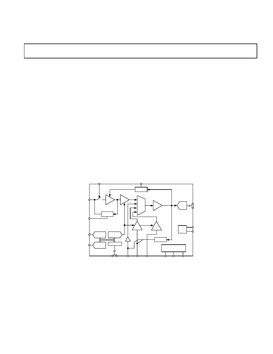
Complete 10-Bit 18 MSPS
CCD Signal Processor
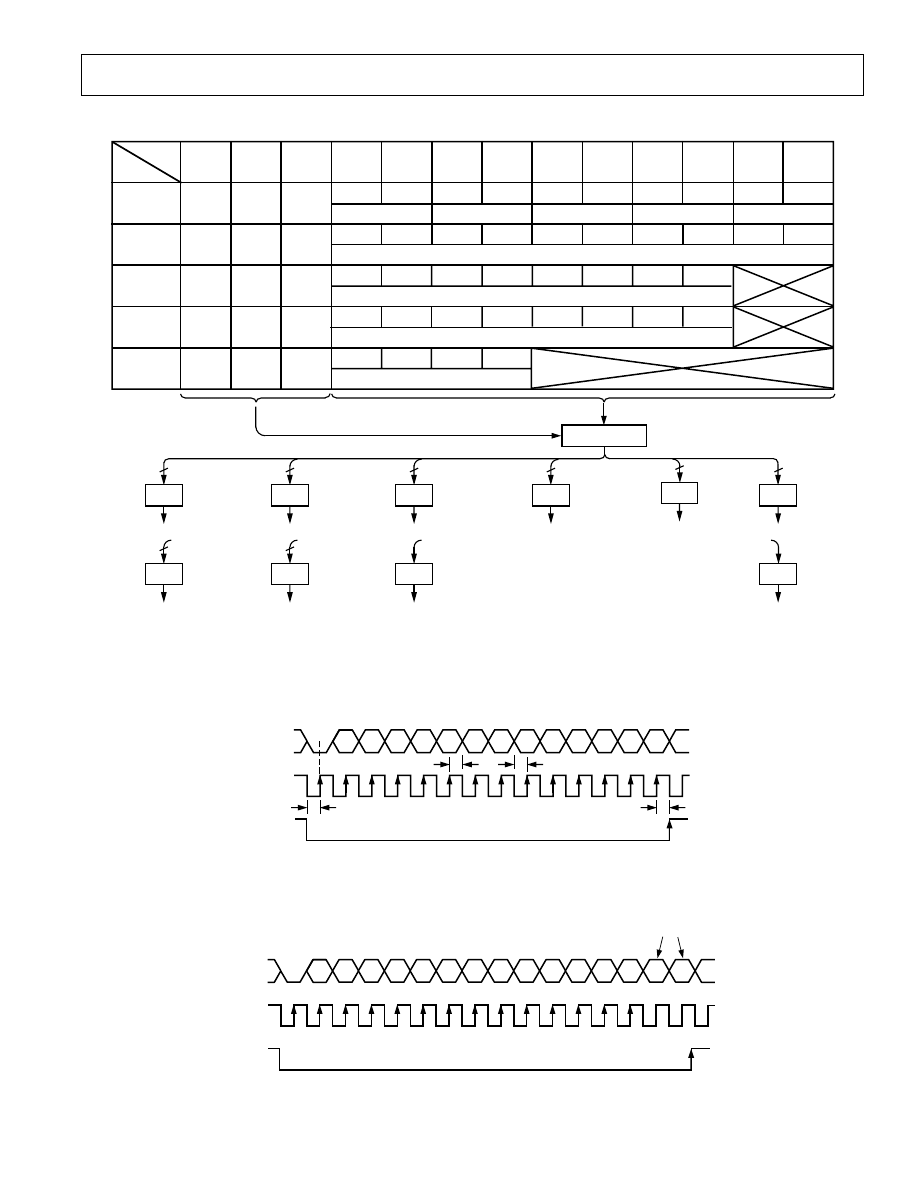
FUNCTIONAL BLOCK DIAGRAM
PGA
0dB
~
34dB
0dB
~
15dB
CLAMP
3
REF
10-BIT
DAC
INTF
AD9806
10
PBLK
CLPOB
3-W INTF
ADCIN AUXIN
SHP
SHD ADCCLK
DOUT
VRT
VRB
CCDIN
DAC1
DAC2
CLPDM
TIMING
GENERATOR
MUX
S/H
CDS
ADC
8-BIT
DAC
8-BIT
DAC
AUXMID
–4
~
14dB
PGA
PGA
CLAMP
CLAMP
FEATURES
Pin-Compatible with Industry Standard AD9803
18 MSPS Correlated Double Sampler (CDS)
Low Noise PGA with 0 dB to 34 dB Gain Range
Low Noise Clamp Circuits
Analog Preblanking Function
10-Bit 18 MSPS A/D Converter
AUX Input with Input Clamp and PGA
Direct ADC Input with Input Clamp
AUXMID Input with PGA
3-Wire Serial Interface for Digital Control
Two Auxiliary 8-Bit DACs
3 V Single Supply Operation
Low Power: 65 mW @ 2.7 V Supply
48-Lead LQFP Package
APPLICATIONS
Camcorders (8 mm and DVC)
Digital Still Cameras
PRODUCT DESCRIPTION
The AD9806 is a complete analog signal processor for CCD
applications. It features an 18 MHz single-channel architecture
designed to sample and condition the outputs of interlaced and
progressive scan area CCD arrays. The AD9806’s signal chain
consists of an input clamp, correlated double sampler (CDS),
digitally programmable gain amplifier (PGA), black level clamp,
and 10-bit A/D converter. Additional input modes are provided
for processing analog video signals.
The internal registers are programmed through a 3-wire serial
digital interface. Programmable features include gain adjust-
ment, black level adjustment, input configuration, and power-
down modes.
The AD9806 operates from a single 3 V power supply, typically
dissipating 75 mW. Packaged in a space-saving 48-lead LQFP,
the AD9806 is specified over an operating temperature range of
–20
°C to +85 C.
REV. 0
–2–
AD9806–SPECIFICATIONS
GENERAL SPECIFICATIONS
Parameter
Min
Typ
Max
Unit
TEMPERATURE RANGE
Operating
–20
+85
°C
Storage
–65
+150
°C
POWER SUPPLY VOLTAGE
(For Functional Operation)
2.7
3.6
V
Analog, Digital, Digital Driver
POWER CONSUMPTION
(Selected through Serial Interface D-Reg)
Normal Operation (D-Reg 00)
(Specified Under Each Mode of Operation)
High-Speed AUX Mode (D-Reg 01)
(Specified Under AUX-Mode)
Reference Standby (D-Reg 10)
5
mW
Total Shut-Down Mode (D-Reg 11)
1
mW
MAXIMUM CLOCK RATE
(Specified Under Each Mode of Operation)
MHz
A/D CONVERTER
Resolution
10
Bits
Differential Nonlinearity (DNL)
±0.5
±1.0
LSB
No Missing Codes
GUARANTEED
Full-Scale Input Voltage
1.0
V
VOLTAGE REFERENCE
Reference Top Voltage (VRT)
2.0
V
Reference Bottom Voltage (VRB)
1.0
V
Specifications subject to change without notice.
DIGITAL SPECIFICATIONS
Parameter
Symbol
Min
Typ
Max
Unit
LOGIC INPUTS
High Level Input Voltage
V
IH
2.1
V
Low Level Input Voltage
V
IL
0.6
V
High Level Input Current
I
IH
10
µA
Low Level Input Current
I
IL
10
µA
Input Capacitance
C
IN
10
pF
LOGIC OUTPUTS
High Level Output Voltage (I
OH
= 2 mA)
V
OH
2.2
V
Low Level Output Voltage (I
OL
= 2 mA)
V
OL
0.5
V
SERIAL INTERFACE TIMING (Figure 7)
Maximum SCLK Frequency
10
MHz
SDATA to SCLK Setup
t
DS
10
ns
SCLK to SDATA Hold
t
DH
10
ns
SLOAD to SCLK Setup
t
LS
10
ns
SCLK to SLOAD Hold
t
LH
10
ns
Specifications subject to change without notice.
(T
MIN
to T
MAX
, AVDD = DVDD = 3.0 V, f
ADCCLK
= 18 MHz, unless otherwise noted.)
(DRVDD = 2.7 V, C
L
= 20 pF.)
REV. 0
–3–
AD9806
CCD-MODE SPECIFICATIONS
Parameter
Min
Typ
Max
Unit
POWER CONSUMPTION
V
DD
= 2.7
65
mW
V
DD
= 3.0
75
mW
V
DD
= 3.3
85
mW
MAXIMUM CLOCK RATE
18
MHz
CDS
Gain
0
dB
Allowable CCD Reset Transient
1
500
mV
Max Input Range before Saturation
1
1000
mV p-p
PGA
Gain Control Resolution
10
Bits
Gain Range (See Figure 5a for Gain Curve)
Low Gain (Code 95)
2
–1
0
+1
dB
Max Gain (1023)
2
32
33
34
dB
BLACK LEVEL CLAMP
Clamp Level (Selected through Serial Interface E-Reg)
CLP0 (E-Reg 00)
32
LSB
CLP1 (E-Reg 01)
48
LSB
CLP2 (E-Reg 10)
64
LSB
CLP3 (E-Reg 11)
16
LSB
SIGNAL-TO-NOISE RATIO
3
(@ Low PGA Gain)
74
dB
TIMING SPECIFICATIONS
4
Pipeline Delay
9
Cycles
Internal Clock Delay
5
(t
ID
)
3
ns
Inhibited Clock Period (t
INHIBIT
)
10
ns
Output Delay (t
OD
)
14.5
16
ns
Output Hold Time (t
HOLD
)
6
ns
ADCCLK, SHP, SHD Clock Period
47
55.6
ns
ADCCLK High-Level/Low-Level
20
28
ns
SHP, SHD Minimum Pulsewidth
10
14
ns
SHP Rising Edge to SHD Rising Edge
20
28
ns
NOTES
1
Input signal characteristics defined as follows:
1V MAX
INPUT
SIGNAL RANGE
200mV MAX
OPTICAL
BLACK PIXEL
500mV TYP
RESET
TRANSIENT
2
Use equations on page 8 to calculate gain.
3
SNR = 20 log
10
(Full-Scale Voltage/RMS Output Noise).
4
20 pF loading; timing shown in Figure 1.
5
Internal aperture delay for actual sampling edge.
Specifications subject to change without notice.
(T
MIN
to T
MAX
, AVDD = DVDD = 3.0 V, f
ADCCLK
= f
SHP
= f
SHD
= 18 MHz, unless otherwise noted.)
REV. 0
–4–
AD9806–SPECIFICATIONS
AUX-MODE SPECIFICATIONS
Parameter
Min
Typ
Max
Unit
POWER CONSUMPTION
Normal (D-Reg 00)
50
mW
High-Speed (D-Reg 01)
95
mW
MAXIMUM CLOCK RATE
Normal (D-Reg 00)
18
MHz
High-Speed (D-Reg 01)
28.6
MHz
PGA (Gain Selected through Serial Interface F-Reg)
Max Input Range
700
mV p-p
Max Output Range
1000
mV p-p
Gain Control Resolution
7
Bits
Gain Range
Min Gain (Code 128)
–2
dB
Max Gain (Code 255)
15
dB
ACTIVE CLAMP
Clamp Level (Selected through Serial Interface E-Reg)
CLP0 (E-Reg 00)
32
LSB
CLP1 (E-Reg 01)
48
LSB
CLP2 (E-Reg 10)
64
LSB
CLP3 (E-Reg 11)
16
LSB
TIMING SPECIFICATIONS
1
Pipeline Delay
9
Cycles
Internal Clock Delay (t
ID
)
Output Delay (t
OD
)
14.5
16
ns
Output Hold Time (t
HOLD
)
7
ns
NOTES
1
20 pF loading; timing shown in Figure 2.
Specifications subject to change without notice.
AUXMID-MODE SPECIFICATIONS
Parameter
Min
Typ
Max
Unit
POWER CONSUMPTION
50
mW
MAXIMUM CLOCK RATE
18
MHz
PGA (Gain Selected through Serial Interface F-Reg)
Max Input Range
700
mV p-p
Max Output Range
1000
mV p-p
Gain Control Resolution
9
Bits
Gain Range (See Figure 5b for Gain Curve)
Min Gain (Code 512)
–4
dB
Max Gain (Code 1023)
14
dB
MIDSCALE OFFSET LEVEL (AT MAX PGA GAIN)
462
512
562
LSB
TIMING SPECIFICATIONS
1
Pipeline Delay
9
Cycles
Internal Clock Delay (t
ID
)
Output Delay (t
OD
)
14.5
16
ns
Output Hold Time (t
HOLD
)
7
ns
NOTES
1
20 pF loading; timing shown in Figure 2.
Specifications subject to change without notice.
(T
MIN
to T
MAX
, AVDD = DVDD = 3.0 V, f
ADCCLK
= 18 MHz, unless otherwise noted.)
(T
MIN
to T
MAX
, AVDD = DVDD = 3.0 V, f
ADCCLK
= 18 MHz, unless otherwise noted.)
REV. 0
–5–
AD9806
ADC-MODE SPECIFICATIONS
Parameter
Min
Typ
Max
Unit
POWER CONSUMPTION
(Same as AUX-MODE)
MAXIMUM CLOCK RATE
(Same as AUX-MODE)
ACTIVE CLAMP
(Same as AUX-MODE)
TIMING SPECIFICATIONS
1
(Same as AUX-MODE)
Specifications subject to change without notice.
DAC SPECIFICATIONS (DAC1 and DAC2)
Parameter
Min
Typ
Max
Unit
RESOLUTION
8
Bits
MIN OUTPUT
0.1
V
MAX OUTPUT
VDD – 0.1
V
MAX CURRENT LOAD
1
mA
MAX CAPACITIVE LOAD
500
pF
Specifications subject to change without notice.
ABSOLUTE MAXIMUM RATINGS
Parameter
With Respect To
Min
Max
Unit
AVDD1, AVDD2
AVSS
–0.3
+3.9
V
DVDD1, DVDD2
DVSS
–0.3
+3.9
V
DRVDD
DRVSS
–0.3
+3.9
V
Digital Outputs
DRVSS
–0.3
DRVDD + 0.3
V
SHP, SHD, DATACLK
DVSS
–0.3
DVDD + 0.3
V
CLPOB, CLPDM, PBLK
DVSS
–0.3
DVDD + 0.3
V
SCK, SL, SDATA
DVSS
–0.3
DVDD + 0.3
V
VRT, VRB, CMLEVEL
AVSS
–0.3
AVDD + 0.3
V
CCDIN, CLPOUT, CLPREF, CLPBYP
AVSS
–0.3
AVDD + 0.3
V
Junction Temperature
150
°C
Lead Temperature (10 sec)
300
°C
ORDERING GUIDE
Model
Temperature Range
Package Description
Package Option
AD9806KST
–20
°C to +85°C
Thin Plastic Quad Flatpack (LQFP)
ST-48
THERMAL CHARACTERISTICS
Thermal Resistance
48-Lead LQFP Package
θ
JA
= 92
°C
(T
MIN
to T
MAX
, AVDD = DVDD = 3.0 V, f
ADCCLK
= 18 MHz, unless otherwise noted.)
CAUTION
ESD (electrostatic discharge) sensitive device. Electrostatic charges as high as 4000 V readily
accumulate on the human body and test equipment and can discharge without detection. Although
the AD9806 features proprietary ESD protection circuitry, permanent damage may occur on
devices subjected to high-energy electrostatic discharges. Therefore, proper ESD precautions are
recommended to avoid performance degradation or loss of functionality.
WARNING!
ESD SENSITIVE DEVICE
REV. 0
AD9806
–6–
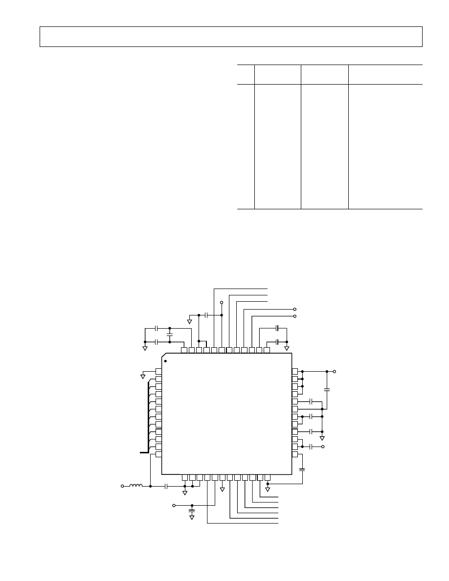
PIN CONFIGURATION
36
35
34
33
32
31
30
29
28
27
26
25
13 14 15 16 17 18 19 20 21 22 23 24
1
2
3
4
5
6
7
8
9
10
11
12
48 47 46 45 44
39 38 37
43 42 41 40
PIN 1
IDENTIFIER
TOP VIEW
(Not to Scale)
DVDD
DVSS
NC
ADCCLK
STBY
NC
(LSB) D0
D1
D2
D3
D4
D5
D6
D7
D8
(MSB) D9
DRVDD
PBLK
CLPOB
SHP
SHD
AD9806
NC
ADCIN
AUXMID
AUXIN
ACVDD
CLPBYP
ACVSS
NC
NC
CLPREF
NC
CCDIN
CLPOUT
VRT
VRB
SUBST
ADVSS
SDATA
ADVDD
SCK
SL
DAC2
DAC1
NC
CMLEVEL
CLPDM
DRVSS
NC = NO CONNECT
PIN FUNCTION DESCRIPTIONS
Pin No.
Mnemonic
Type
Description (See Figures 10 and 11 for Circuit Configurations)
1, 15, 24
NC
No Connect (Should be Left Floating or Tied to Ground)
2–11
D0–D9
DO
Digital Data Outputs
12
DRVDD
P
Digital Driver Supply (3 V)
13
DRVSS
P
Digital Driver Ground
14
DVSS
P
Digital Ground
16
ADCCLK
DI
ADC Sample Clock Input
17
DVDD
P
Digital Supply (3 V)
18
STBY
DI
Power-Down Mode (Active High/Internal Pull-Down). Enables Reference Standby Mode.
19
PBLK
DI
Pixel Blanking
20
CLPOB
DI
Black Level Restore Clamp
21
SHP
DI
CCD Reference Sample Clock Input
22
SHD
DI
CCD Data Sample Clock Input
23
CLPDM
DI
Input Clamp
25
CLPOUT
AO
CDS Bypass (0.1
µF to Ground)
26
CCDIN
AI
CDS Input Pin (Connect to CCD Input Signal through 0.1
µF Capacitor)
27
NC
No Connect (Should Be Left Floating, or May Be Shorted to Pin 26)
28
CLPREF
AO
CDS Bypass (0.1
µF to Ground)
29, 30, 38
NC
No Connect (Should Be Left Floating, Tied to Ground, or Decoupled to Ground)
31
ACVSS
P
Analog Ground
32
CLPBYP
AO
CDS Bypass (0.1
µF to Ground)
33
ACVDD
P
Analog Supply (3 V)
34
AUXIN
AI
AUX-MODE Input
35
AUXMID
AI
AUXMID-MODE Input
36
ADCIN
AI
ADC-MODE Input
37
CMLEVEL
AO
Common-Mode Level (0.1
µF to Ground)
39
DAC1
AO
DAC1 Output
40
DAC2
AO
DAC2 Output
41
SL
DI
Serial I/F Load Signal
42
SCK
DI
Serial I/F Clock
43
ADVDD
P
Analog Supply (3 V)
44
SDATA
DI
Serial I/F Input Data
45
ADVSS
P
Analog Ground
46
SUBST
P
Analog Ground
47
VRB
AO
Bottom Reference (0.1
µF to Ground and 1 µF to VRT)
48
VRT
AO
Top Reference (0.1
µF to Ground)
NOTE
Type: AI = Analog Input, AO = Analog Output, DI = Digital Input, DO = Digital Output, P = Power.
REV. 0
AD9806
–7–
TIMING SPECIFICATIONS
N
N+1
N+2
N+3
N+4
t
INHIBIT
t
ID
t
ID
t
OD
t
HOLD
ADCCLK RISING EDGE PLACEMENT
N–0
N–9
N–8
N–7
N–6
N–5
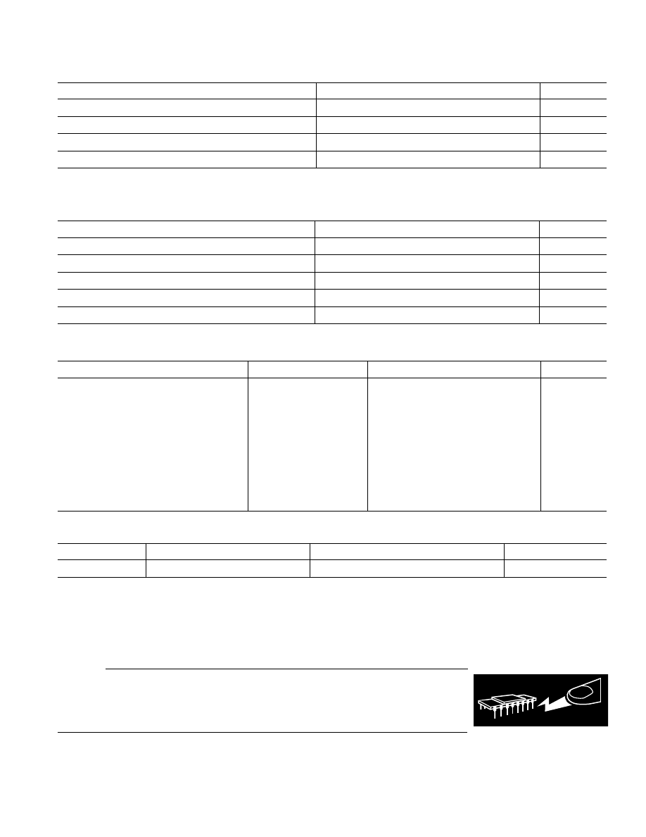
CCD
SHP
SHD
ADCCLK
D0–D9
NOTES:
1. SHP AND SHD SHOULD BE OPTIMALLY ALIGNED WITH THE CCD SIGNAL. SAMPLES ARE TAKEN AT THE RISING EDGES.
2. ADCCLK RISING EDGE MUST OCCUR AT LEAST 15ns AFTER THE RISING EDGE OF SHP (
t
INHIBIT
).
3. RECOMMENDED PLACEMENT FOR ADCCLK RISING EDGE IS BETWEEN THE RISING EDGE OF SHD AND FALLING EDGE OF SHP.
4. OUTPUT LATENCY IS 9 CYCLES.
5. ACTIVE LOW CLOCK PULSE MODE IS SHOWN.
Figure 1. CCD-MODE Timing
t
ID
t
OD
t
HOLD
N
N+1
N+2
N+3
N+4
N–9
N–8
N–7
N+5
VIDEO
INPUT
ADCCLK
D0–D9
N–6
N–5
NOTE:
EXAMPLE OF OUTPUT DATA LATCHED BY ADCCLK RISING EDGE.
Figure 2. AUX-, AUXMID-, ADC-Mode Timing
CCD
SIGNAL
CLPOB
CLPDM
PBLK
EFFECTIVE
PIXELS
OPTICAL BLACK
BLANKING
INTERVAL
DUMMY BLACK
EFFECTIVE
PIXELS
NOTES:
1. CLPOB PULSEWIDTH SHOULD BE A MINIMUM OF 10 OB PIXELS WIDE, 20 OB PIXELS ARE RECOMMENDED.
2. CLPDM PULSEWIDTH SHOULD BE AT LEAST 1
s WIDE.
3. PBLK IS NOT REQUIRED, BUT RECOMMENDED IF THE CCD SIGNAL AMPLITUDE EXCEEDS 1V p-p.
4. CLPDM OVERWRITES PBLK.
5. ACTIVE LOW CLAMP PULSE MODE IS SHOWN.
Figure 3. CCD-MODE Clamp Timing
REV. 0
AD9806
–8–
PGA GAIN REGISTER CODE
34
0
PGA GAIN
–
dB
127
255
383
511
639
767
895
1023
28
22
16
10
4
–2
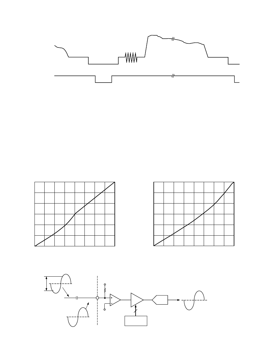
Figure 5a. PGA Gain Curve for CCD-Mode
AUXMID
0.1
F
PGA GAIN
REGISTER
9
5k
⍀
0.4V
0.4V
INPUT SIGNAL
??V
0.8V
0.4V
–4 dB TO +14dB
PIN 35
PGA
ADC
MIDSCALE
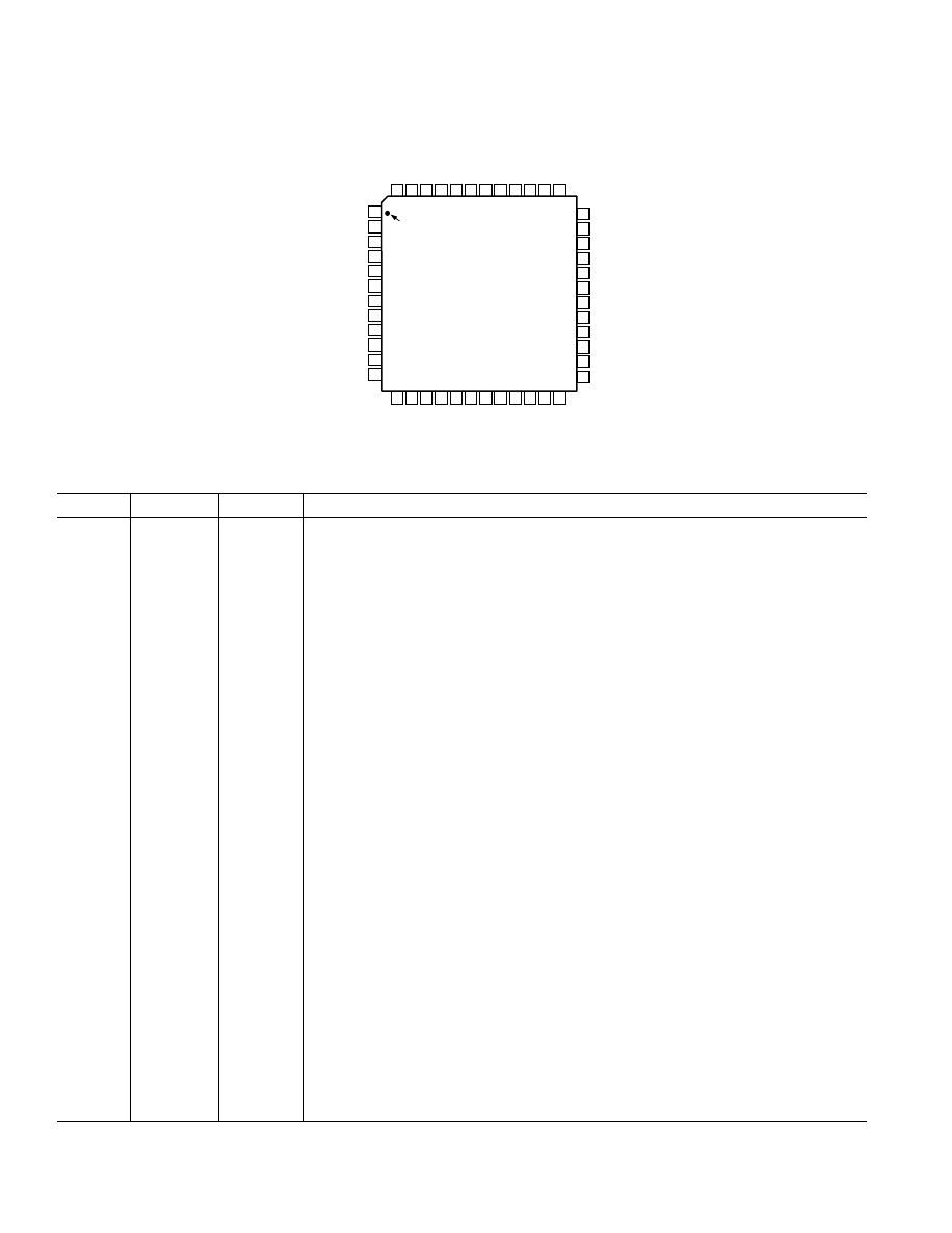
Figure 6. AUXMID-Mode Circuit Block Diagram
H
SYNC
INTERNAL CLAMPING
OCCURS DURING SYNC
VIDEO
SIGNAL
INPUT
CLAMP INTERVAL
(AD9806 INTERNAL
SIGNAL)
NOTE: The AD9806 uses an “automatic” video clamp that senses the most negative in the input signal and uses this level to set the clamp voltage.
As shown in the video waveform above, the SYNC level will be clamped to the black level specified in the E-Register.
Figure 4. AUX-MODE and ADC-MODE Clamp Operation
PGA GAIN REGISTER CODE
14
PGA GAIN
–
dB
639
767
895
1023
11
8
5
2
–1
512
–4
Figure 5b. PGA Gain Curve for AUXMID-Mode
PGA GAIN CURVE DETAILS
In CCD-Mode, the AD9806 PGA stage provides a gain range
of 0 dB to 34 dB, programmable with 10-bit resolution through
the serial digital interface. The PGA gain curve is divided into
two separate regions. When the PGA Gain Register code is
between 0, and 511, the curve follows a (1 + x)/(1 – x) shape,
which is similar to a “linear-in-dB” characteristic. From Code
512 to Code 1023, the curve follows a “linear-in-dB” shape. In
AUXMID-Mode, the PGA provides a gain range of –4 dB to
+14 dB, programmable with 9-bit resolution. The exact PGA
gain for either mode can be calculated for any Gain Register
value by using the following equations:
TIMING SPECIFICATIONS (Continued)
CCD-MODE
Code Range Gain Equation (dB)
0–511
Gain = 20 log
10
([658 + code]/[658 – code]) – 2.4
512–1023
Gain = (0.0354)(code) – 2.4
AUXMID-MODE
Code Range Gain Equation (dB)
512–1023
Gain = 20 log
10
([146 + code]/[1170 – code]) – 4
REV. 0
AD9806
–9–
SERIAL INTERFACE SPECIFICATIONS
MODES2
1
SDATA
SELECT
DAC2
DAC1
PGA
MODES
A0
0
A1
1
A2
0
D0
D1
D2
D3
D4
D5
D6
D7
D8
D9
e0
e1
d0
d1
c0
c1
b0
b1
a0
a1
CLAMP
LEVEL
POWER-DOWN
MODES
CLOCK
MODES
OUTPUT
MODES
OPERATION
MODES
f0
f1
f2
f3
f4
f5
f6
f7
f8
f9
PGA GAIN LEVEL SELECTION
g0
g1
g2
g3
g4
g5
g6
g7
h0
h1
h2
h3
h4
h5
h6
h7
m0
0*
j0
DAC1 INPUT
DAC2 INPUT
OPERATION AND
POWER-DOWN MODES
SHIFT REGISTER
F-REG
f0–f9
E-REG
e0–e1
D-REG
(d) POWER-DOWN MODES
d0–d1
C-REG
c0–c1
B-REG
b0–b1
A-REG
(a) OPERATION MODES
a0–a1
(b) OUTPUT MODES
(c) CLOCK MODES
(e) CLAMP LEVEL
(f) PGA GAIN
M-REG
m0
J-REG
j0
H-REG
h0–h7
G-REG
(g) DAC1 INPUT
g0–g7
(h) DAC2 INPUT
(j) EVEN-ODD OFFSET
CORRECTION
(m) DAC1 AND DAC2
POWER-DOWN
SELECT
*NOTE: MODES2 REGISTER BIT D1 MUST BE SET TO ZERO
DON'T
CARE
1
1
1
1
1
1
1
0
0
0
0
0
Figure 7. AD9806 Internal Register Map
RISING EDGE
TRIGGERED
t
DH
t
LS
t
LH
REGISTER LOADED ON
RISING EDGE
RNW
A0
A1
A2
D0
D1
D2
D3
D4
D5
D6
D7
D8
D9
SDATA
SCK
SL
t
DS
Figure 8. Serial WRITE Operation
SDATA
RNW
A0
A1
A2
D0
D1
D2
D3
D4
D5
D6
D7
D8
D9
XX
XX
DUMMY BITS
IGNORED
SCK
SL
Figure 9. 16-Bit Serial WRITE Operation
REV. 0
AD9806
–10–
REGISTER DESCRIPTION
(a)
A-REGISTER: Modes of Operation
(Power-On Default
Value = 11)
a1
a0
Modes
0
0
ADC-MODE
0
1
AUX-MODE
1
0
AUXMID-MODE
1
1
CCD-MODE
(b) B-REGISTER: Output Modes
(Default = 00)
b1
b0
D9 D8 D7 D6 D5 D4 D3 D2 D1 D0
0
0
Normal
0
1
0
1
0
1
0
1
0
1
0
1
1
0
1
0
1
0
1
0
1
0
1
0
1
1
High Impedance
(c) C-REGISTER: Clock Modes
(Default = 00)
c1
c0
SHP-SHD Clock Pulses
Clamp Active Pulses
0
0
Active Low
Active Low
0
1
Active Low
Active High
1
0
Active High
Active Low
1
1
Active High
Active High
(d) D-REGISTER: Power-Down Modes
(Default = 00)
Modes
d1
d0 Description
Normal
0
0
Normal Operation
High Speed
0
1
High-Speed AUX/ADC-MODE
Power-Down1
1
0
Reference Stand-By (Same
Mode as STBY Pin 18)
Power-Down2
1
1
Total Shut-Down
(e) E-REGISTER: Clamp Level Selection
(Default = 00)
e1
e0
Clamp Level
CLP (0)
0
0
32 LSBs
CLP (1)
0
1
48 LSBs
CLP (2)
1
0
64 LSBs
CLP (3)
1
1
16 LSBs
(f) F-REGISTER:
CCD-Mode PGA
(Default = 00 . . . 0)
f 9 f 8 f 7 f 6 f 5 f 4 f 3 f 2 f 1 f 0
CCD–Gain
Gain (0)
0 0
0 0 0 0
0 0 0
0
Minimum
Gain (1023) 1 1
1 1 1 1
1 1 1
1
Maximum
f) F-REGISTER:
AUXMID-Mode PGA
(Default = 00 . . . 0)
f 9 f 8 f 7 f 6 f 5 f 4 f 3 f 2 f 1 f 0 AUXMID–Gain
Gain (512)
1 0 0 0 0 0 0 0 0 0
–4 dB
Gain (1023) 1 1 1 1 1 1 1 1 1 1
+14 dB
Only the 9 LSBs of F-REG are used to adjust gain.
(f) F-REGISTER:
AUX-Mode PGA
(Default = 00 . . . 0)
f 9 f 8 f 7 f 6 f 5 f 4 f 3 f 2
AUX-Gain
Gain (128)
1 0 0 0 0 0 0 0
Minimum
Gain (255)
1 1 1 1 1 1 1 1
Maximum
(g) G-REGISTER: DAC1 Input
(Default = 00 . . . 0)
g7 g6 g5 g4 g3 g2 g1 g0
DAC1 Output
Code (0)
0
0
0
0
0
0
0
0
Minimum
Code (255) 1
1
1
1
1
1
1
1
Maximum
(h) H-REGISTER: DAC2 Input
(Default = 00 . . . 0)
h7 h6 h5 h4 h3 h2 h1 h0
DAC2 Output
Code (0)
0
0
0
0
0
0
0
0
Minimum
Code (255) 1
1
1
1
1
1
1
1
Maximum
(j) J-REGISTER:
Even-Odd Offset Correction
(Default = 0)
j0
Even-Odd Offset Correction
0
Offset Correction In Use
1
Offset Correction Not Used
(m) M-REGISTER: DAC1 and DAC2 PDN
(Default = 0)
m0
Power-Down of 8-Bit DACs
0
8-Bit DACs Powered Down
1
8-Bit DACs Operational
NOTE: With the exception of a write to the PGA register dur-
ing AUX-mode, all data writes must be 10 bits. During an
AUX-mode write to the PGA register, only 8 bits of data are
required. If more than 14 SCK rising edges are applied during a
write operation, additional SCK pulses will be ignored (see
Figure 9). All reads must be 10 bits to receive valid register
contents. All registers default to 0s on power-up, except for the
A-register which defaults to 11. Thus, on power-up, the AD9806
defaults to CCD mode with the 8-bit DACs powered down. Dur-
ing the power-up phase, it is recommended that SL be HIGH
and SCK be LOW to prevent accidental register write operations.
SDATA may be unknown. The RNW bit (“Read/Not Write”)
must be LOW for all write operations to the serial interface, and
HIGH when reading back from the serial interface registers.
REV. 0
AD9806
–11–
APPLICATION INFORMATION
Grounding and Decoupling Recommendations
As shown in Figure 10, a single ground plane is recommended
for the AD9806. This ground plane should be as continuous as
possible, particularly around Pins 25 through 37. This will ensure
that all analog decoupling capacitors provide the lowest possible
impedance path between the power and bypass pins and their
respective ground pins. All decoupling capacitors should be
located as close as possible to the package pins. A single clean
power supply is recommended for the AD9806, but a separate
digital driver supply may be used for DRVDD (Pin 12). DRVDD
should always be decoupled to DRVSS (Pin 13), which should
be connected to the analog ground plane. The advantages of
using a separate digital driver supply include using a lower volt-
age (2.7 V) to match levels with a 2.7 V ASIC, reducing digital
power dissipation, and reducing potential noise coupling.
Using the AD9806 in AD9803 Sockets
The AD9806 may be easily used in existing AD9803 designs
without any circuit modifications. Most of the pin assignments
are the same for both ICs. Table I outlines the differences. The
circuit of Figure 10 shows the necessary connections for the
AD9806 when used in an existing AD9803 socket. If the two
auxiliary DACs are not used, then Pins 39 and 40 (DAC1 and
DAC2) may be grounded. If the AUX or ADC modes are needed,
then the input signal should be connected to either AUXIN or
ADCIN through a 0.1
µF capacitor, in the same way that
CCDIN is used with the input signal.
Table I. AD9806/AD9803 Pin Differences
Pin
No.
AD9803
AD9806
Circuit Connection
1
NC
NC
Ground
15
ACLP
NC
Ground
24
NC
NC
Ground
25
CCDBYP2
CLPOUT
Decoupled with 0.1
µF
to Ground
27
PIN
NC
Shorted to Pin 26
28
CCDBYP2
CLPREF
Decoupled with 0.1
µF
to Ground
29
PGABYP1
NC
Decoupled with 0.1
µF
to Ground
30
PGABYP2
NC
Shorted to Pin 29
35
AUXCONT
AUXMID
Ground, or decoupled
with 0.1
µF to Ground
38
VTRBYP
NC
Decoupled with 0.1
µF
to Ground
Using the AD9806 in New Designs
Figure 11 shows the recommended circuit for using the AD9806
in new designs. Three external decoupling capacitors have been
removed from the circuit shown in Figure 9, one from Pin 29,
one from Pin 38, and one from between Pins 47 and 48. Note
that the decoupling capacitors for Pins 47 (VRB) and 48 (VRT)
must be increased to 1.0
µF when used in this configuration.
0.1
F
0.1
F
0.1
F
0.1
F
0.1
F
CCD
SIGNAL
INPUT
V
DD
0.1
F
DIGITAL
OUTPUT
DATA
48
47
46
45
44
39 38
37
43
42
41 40
1
2
3
4
5
6
7
8
9
10
11
12
NC
D0 (LSB)
D1
D2
D3
D4
D5
D6
D7
D8
D9 (MSB)
DRVDD
AD9806
13 14
15
16
17
18
19
20
21 22
23
24
DVDD
DVSS
NC
ADCCLK
STBY
PBLK
CLPOB
SHP
SHD
NC
VRT
VRB
SUBST
ADVSS
SDATA
ADVDD
SCK
SL
DAC2
DAC1
NC
CMLEVEL
CLPDM
DRVSS
36
35
34
33
32
31
30
29
28
27
26
25
ADCIN
AUXMID
AUXIN
ACVDD
CLPBYP
ACVSS
NC
NC
CLPREF
NC
DIN
CLPOUT
NC = NO CONNECT
0.1
F
V
DD
V
DD
0.1
F
CLPDM
SHD
SHP
CLPOB
PBLK
ADCCLK
0.1
F
0.1
F
VOUT1
VOUT2
SDATA
SCK
SL
0.1
F
0.1
F
1.0
F
0.1
F
V
DD
Figure 10. CCD-Mode Circuit Configuration Used in AD9803 Socket
REV. 0
–12–
C02197–2.5–1/01 (rev. 0)
PRINTED IN U.S.A.
AD9806
OUTLINE DIMENSIONS
Dimensions shown in inches and (mm).
48-Lead, LQFP
(ST-48)
TOP VIEW
(PINS DOWN)
1
12
13
25
24
36
37
48
0.019 (0.5)
BSC
0.276
(7.00)
BSC
SQ
0.011 (0.27)
0.006 (0.17)
0.354 (9.00) BSC SQ
0.063 (1.60)
MAX
0.030 (0.75)
0.018 (0.45)
0.008 (0.2)
0.004 (0.09)
0
ⴗ
MIN
COPLANARITY
0.003 (0.08)
SEATING
PLANE
0.006 (0.15)
0.002 (0.05)
7
ⴗ
0
ⴗ
0.057 (1.45)
0.053 (1.35)
0.1
F
0.1
F
0.1
F
0.1
F
CCD
SIGNAL
INPUT
V
DD
0.1
F
DIGITAL
OUTPUT
DATA
48
47
46
45
44
39 38
37
43
42
41 40
NC
D0 (LSB)
D1
D2
D3
D4
D5
D6
D7
D8
D9 (MSB)
DRVDD
AD9806
13 14
15
16
17
18
19
20
21 22
23
24
DVDD
DVSS
NC
ADCCLK
STBY
PBLK
CLPOB
SHP
SHD
NC
VRT
VRB
SUBST
ADVSS
SDATA
ADVDD
SCK
SL
DAC2
DAC1
NC
CMLEVEL
CLPDM
DRVSS
36
35
34
33
32
31
30
29
28
27
26
25
ADCIN
AUXMID
AUXIN
ACVDD
CLPBYP
ACVSS
NC
NC
CLPREF
NC
DIN
CLPOUT
NC = NO CONNECT
0.1
F
V
DD
V
DD
0.1
F
CLPDM
SHD
SHP
CLPOB
PBLK
ADCCLK
0.1
F
VOUT1
VOUT2
SDATA
SCK
SL
1.0
F
0.1
F
V
DD
1.0
F
1
2
3
4
5
6
7
8
9
10
11
12
Figure 11. CCD-Mode Circuit Configuration Using Minimum External Components
Wyszukiwarka
Podobne podstrony:
LCD & CCD, AD9882 pra
LCD & CCD, AD9882 brief
LCD & CCD, AD9882 pra
LCD & CCD, AD9882 brief
lcd
LCD F PCB
DSC PC5010 v2 0 obs lcd
Grundig TV Lcd
Monitor HP Lcd
Instrukcja CCD 2001 w 1000, A4, W2 04
AVT1615 AVTduino LCD
Proview RA783 LCD Service Manual
6 ARM obsluga LCD Nieznany
Proview PZ456 LCD Service Manual
CURSO MONITOR LCD
Obsługa wyświetlacza Lcd z układem sterowania Hd44780U
Proview SH770I LCD Service Manual
więcej podobnych podstron