Preliminary Technical Data
PRELIMINARY TECHNICAL DATA
Rev. PrA
a
Information furnished by Analog Devices is believed to be accurate and
reliable. However, no responsibility is assumed by Analog Devices for its
use, nor for any infringements of patents or other rights of third parties that
may result from its use. No license is granted by implication or otherwise
under any patent or patent rights of Analog Devices.
One Technology Way, P.O. Box 9106, Norwood, MA 02062-9106, U.S.A.
Tel: 781/329-4700
www.analog.com
Fax: 781/326-8703
© Analog Devices, Inc., 2002
AD9882
Dual Interface for
Flat Panel Displays
FEATURES
Analog Interface
140 MSPS Maximum Conversion Rate
Programmable Analog Bandwidth
0.5 V to 1.0 V Analog Input Range
500 ps p-p PLL Clock Jitter at 140 MSPS
3.3 V Power Supply
Full Sync Processing
Midscale Clamping
4:2:2 Output Format Mode
Digital Interface
DVI 1.0 Compatible Interface
112 MHz Operation
High Skew Tolerance of 1 Full Input Clock
Sync Detect for “Hot Plugging”
Supports High-Bandwidth Digital Content Protection
APPLICATIONS
LCD Monitors and Projectors
Plasma Display Panels
Scan Converter
Microdisplays
Digital TV
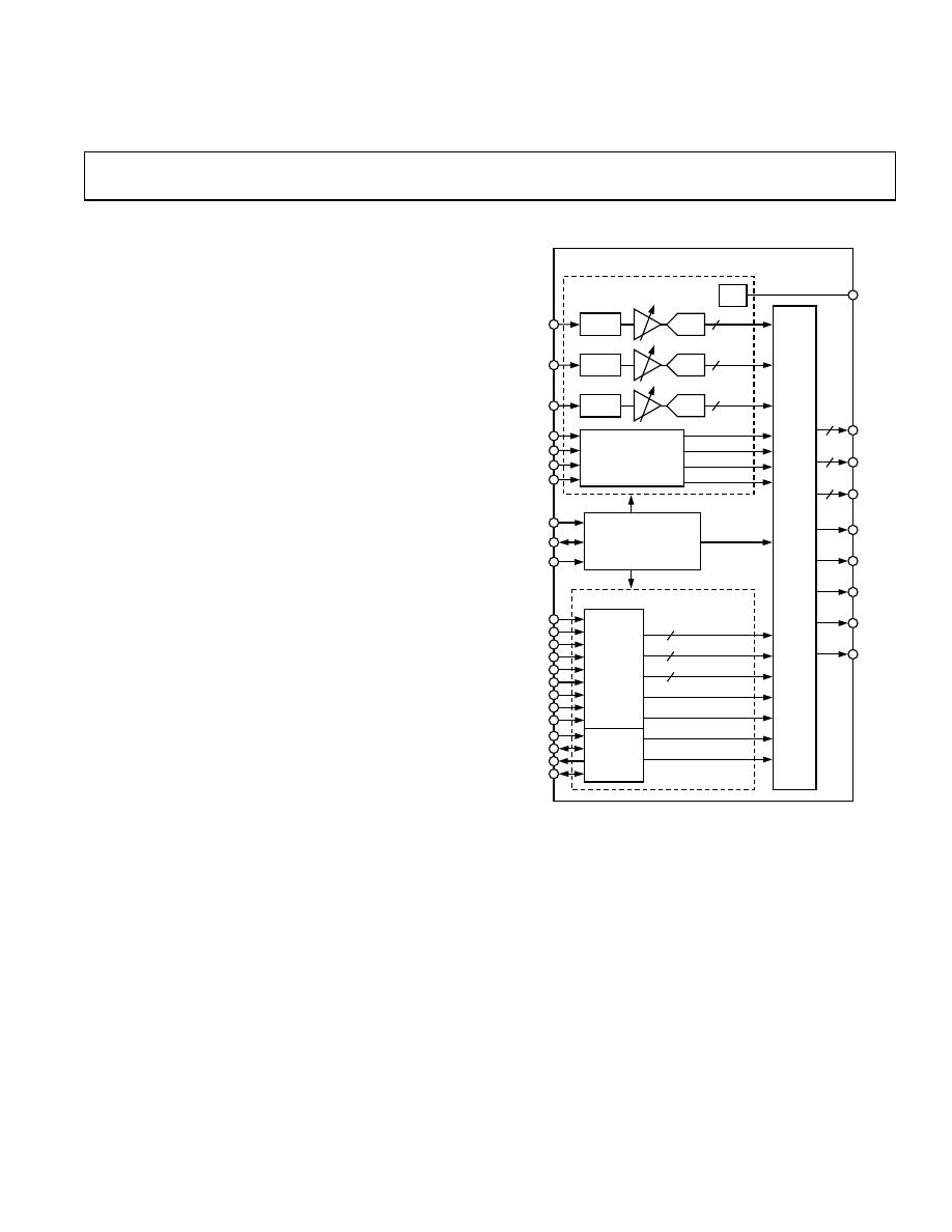
FUNCTIONAL BLOCK DIAGRAM
A/D
CLAMP
R
AIN
8
R
OUT
A/D
CLAMP
G
AIN
8
G
OUT
A/D
CLAMP
B
AIN
8
B
OUT
ANALOG INTERFACE
SOGIN
HSYNC
FILT
VSYNC
SYNC
PROCESSING AND
CLOCK
GENERATION
MUXES
DATACK
HSOUT
VSOUT
SOGOUT
8
REF
REFBYPASS
R
OUT
8
G
OUT
8
B
OUT
DATACK
HSOUT
VSOUT
SOGOUT
DE
SCL
SERIAL REGISTER AND
POWER MANAGEMENT
SDA
A
0
DIGITAL INTERFACE
DVI
RECEIVER
HDCP
RX0+
RX0–
RX1+
RX1–
RX2+
RX2–
RXC+
RXC–
R
TERM
DDCSCL
DDCSDA
MCL
MDA
8
8
8
R
OUT
G
OUT
B
OUT
DATACK
DE
HSYNC
VSYNC
AD9882
GENERAL DESCRIPTION
The AD9882 offers designers the flexibility of an analog inter-
face and Digital Visual Interface (DVI) receiver integrated on a
single chip. Also included is support for High-Bandwidth Digital
Content Protection (HDCP).
Analog Interface
The AD9882 is a complete 8-bit 140 MSPS monolithic analog
interface optimized for capturing RGB graphics signals from
personal computers and workstations. Its 140 MSPS encode
rate capability and full-power analog bandwidth of 300 MHz
supports resolutions up to SXGA (1280
× 1024 at 75 Hz).
The analog interface includes a 140 MHz triple ADC with
internal 1.25 V reference, a Phase Locked Loop (PLL), and
programmable gain, offset, and clamp control. The user provides
only a 3.3 V power supply, analog input, and Hsync. Three-
state CMOS outputs may be powered from 2.5 V to 3.3 V.
The AD9882’s on-chip PLL generates a pixel clock from Hsync.
Pixel clock output frequencies range from 12 MHz to 140 MHz.
PLL clock jitter is 500 ps p-p typical at 140 MSPS. The AD9882
also offers full sync processing for composite sync and Sync-on-
Green (SOG) applications.
Digital Interface
The AD9882 contains a DVI 1.0 compatible receiver and supports
display resolutions up to SXGA (1280
× 1024 at 60 Hz). The
receiver operates with true color (24-bit) panels and also features
an intra-pair skew tolerance of up to one full clock cycle.
With the inclusion of HDCP, displays may now receive encrypted
video content. The AD9882 allows for authentication of a video
receiver, decryption of encoded data at the receiver, and renew-
ability of that authentication during transmission as specified by
the HDCP v1.0 protocol.
Fabricated in an advanced CMOS process, the AD9882 is pro-
vided in a space-saving 100-lead LQFP surface-mount plastic
package and is specified over the 0
°C to 70°C temperature range.

PRELIMINARY TECHNICAL DATA
Rev. PrA
–2–
AD9882
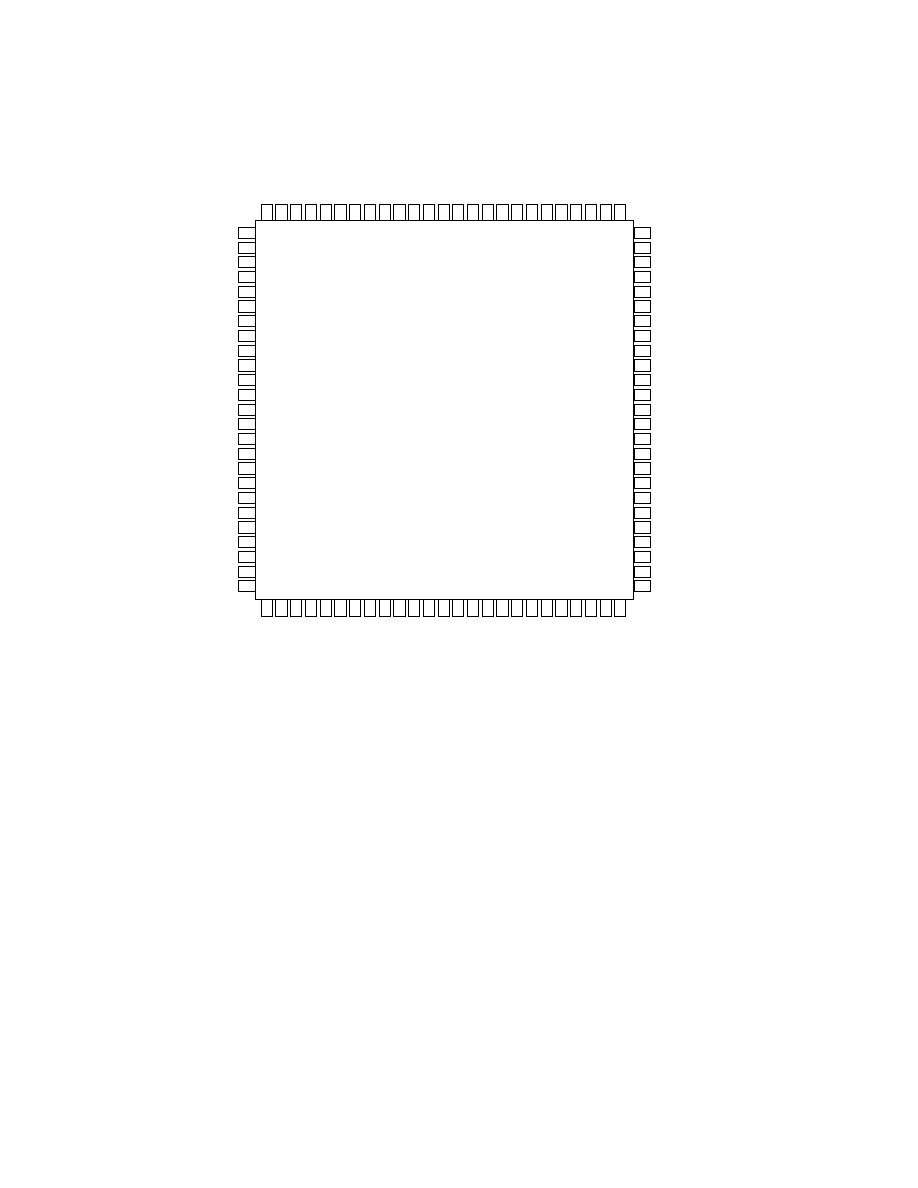
PIN CONFIGURATION
1
GND
GREEN<7>
GREEN<6>
GREEN<5>
GREEN<4>
GREEN<3>
GREEN<2>
GREEN<1>
GREEN<0>
V
DD
GND
BLUE<7>
BLUE<6>
BLUE<5>
BLUE<4>
BLUE<3>
BLUE<2>
BLUE<1>
BLUE<0>
V
DD
GND
CTL 0
CTL 1
CTL 2
CTL 3
2
3
4
5
6
7
8
9
10
11
12
13
14
15
16
17
18
19
20
21
22
23
24
25
26
GND
VD
R
TERM
VD
VD
GND
RX0
–
RX0+
GND
RX1
–
RX1+
GND
RX2
–
RX2+
GND
RXC+
RXC
–
VD
PVD
GND
PVD
GND
FIL
T
PVD
GND
27
28
29
30
31
32
33
34
35
36
37
38
39
40
41
42
43
44
45
46
47
48
49
50
75
74
73
72
71
70
69
68
67
66
65
64
63
62
61
60
59
58
57
56
55
54
53
52
51
GND
MIDBYPASS
REFBYPASS
VD
GND
R
AIN
VD
GND
VD
GND
G
AIN
SOGIN
VD
GND
VD
GND
B
AIN
VD
GND
VD
GND
DDCSDA
DDCSCL
RVD
GND
100
99
98
97
96
95
94
93
92
91
90
89
88
87
86
85
84
83
82
81
80
79
78
77
76
V
DD
RED<0>
RED<1>
RED<2>
RED<3>
RED<4>
RED<5>
RED<6>
RED<7>
GND
VDD
SOGOUT
HSOUT
VSOUT
DE
DA
T
A
C
K
GND
V
DD
MD
A
MCL
VSYNC
HSYNC
SD
A
SCL
A0
TOP VIEW
(Not to Scale)
AD9882

PRELIMINARY TECHNICAL DATA
Rev. PrA
C02889
–0–3/02(PrA)
PRINTED IN U.S.A.
–3–
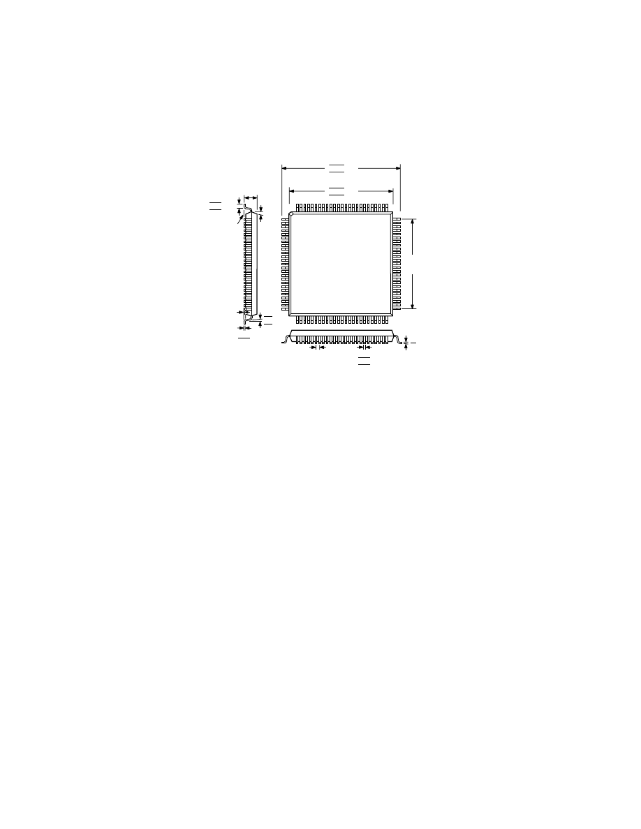
OUTLINE DIMENSIONS
Dimensions shown in millimeters.
100-Lead LQFP Package
(ST-100)
TOP VIEW
(PINS DOWN)
1
25
26
51
50
75
76
100
16.20
16.00 SQ
15.80
14.05
14.00 SQ
13.95
12.00
BSC
0.50 BSC
LEAD PITCH
0.27
0.22 TYP
0.17
LEAD WIDTH
7
ⴗ
0
ⴗ
1.60 MAX
SEATING
PLANE
12
ⴗ
TYP
0.75
0.60 TYP
0.50
0.008
MAX LEAD
COPLANARITY
10
ⴗ
6
ⴗ
2
ⴗ
0.15
0.05
NOTE:
THE ACTUAL POSITION OF EACH LEAD IS WITHIN 0.08 FROM ITS IDEAL
POSITION WHEN MEASURED IN THE LATERAL DIRECTION.
Wyszukiwarka
Podobne podstrony:
LCD & CCD, AD9882 brief
LCD & CCD, AD9882 brief
LCD & CCD, AD9806 0
LCD & CCD, AD9806 0
lcd
2002 10 12 pra
LCD F PCB
DSC PC5010 v2 0 obs lcd
Grundig TV Lcd
Monitor HP Lcd
2008 czerwiec zad 3 Egzamin pra Nieznany
Instrukcja CCD 2001 w 1000, A4, W2 04
AVT1615 AVTduino LCD
Proview RA783 LCD Service Manual
2010 czerwiec zad 5 Egzamin pra Nieznany (2)
6 ARM obsluga LCD Nieznany
Proview PZ456 LCD Service Manual
więcej podobnych podstron