L10: 6.111 Spring 2006
1
Introductory Digital Systems Laboratory
L10: Analog Building Blocks
L10: Analog Building Blocks
(
(
OpAmps
OpAmps
, A/D, D/A)
, A/D, D/A)
Acknowledgement:
Materials in this lecture are courtesy of the following sources and are used with permission.
Dave Wentzloff
L10: 6.111 Spring 2006
2
Introductory Digital Systems Laboratory
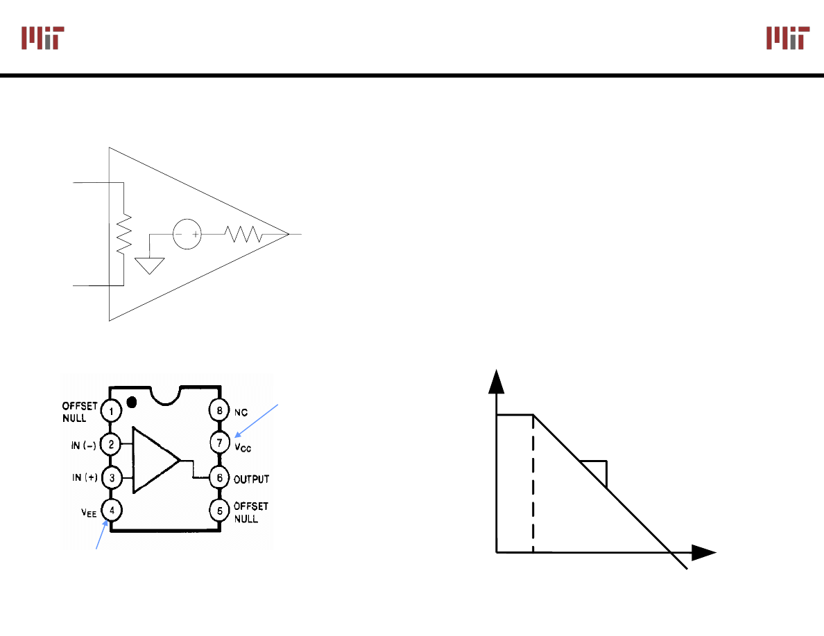
Introduction to Operational Amplifiers
Introduction to Operational Amplifiers
Typically very high input
resistance ~ 300KΩ
High DC gain (~10
5
)
Output resistance ~75Ω
DC Model
LM741 Pinout
in
out
V
f
a
V
⋅
=
)
(
a(f)
f
10Hz
10
5
-20dB/
decade
+10 to +15V
-10 to -15V
id
v
a ⋅
id
v
in
R
out
R
+
−
out
v
Reprinted with
permission of
National
Semiconductor
Corporation.
Reprinted with permission of National Semiconductor Corporation.
L10: 6.111 Spring 2006
3
Introductory Digital Systems Laboratory
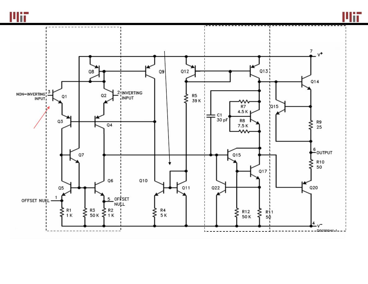
The Inside of a 741
The Inside of a 741
OpAmp
OpAmp
Differential
Input Stage
Additional
Gain Stage
Output Stage
Current Source
for biasing
Bipolar version
has small input
Bias current
MOS OpAmps
have ~ 0 input
current
Gain is Sensitive to Operating Condition
(e.g., Device, Temperature, Power supply voltage, etc.)
Output devices
provides large
drive current
Reprinted with
permission of
National
Semiconductor
Corporation.
Reprinted with permission of National Semiconductor Corporation.
L10: 6.111 Spring 2006
4
Introductory Digital Systems Laboratory
Simple Model for an
Simple Model for an
OpAmp
OpAmp
+
-
i
+
~ 0
i
-
~ 0
+
-
+
-
v
id
v
out
v
out
v
id
V
CC
= 10V
-V
CC
= -10V
ε = 100μV
-100
μV
Reasonable
approximation
+
-
v
id
+
-
av
id
+
-
v
out
Linear Mode
If -V
CC
< v
out
< V
CC
+
-
v
id
-V
CC
+
-
v
out
Negative Saturation
v
id
< -
ε
-
+
+
-
v
id
+
-
v
out
Positive Saturation
v
id
>
ε
-
+
+V
CC
-V
CC
V
CC
Small input range for “Open” loop Configuration
L10: 6.111 Spring 2006
5
Introductory Digital Systems Laboratory
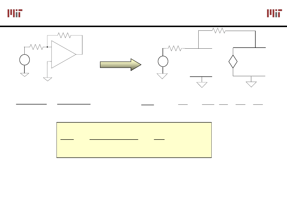
The Power of (Negative) Feedback
The Power of (Negative) Feedback
in
v
out
v
1
R
2
R
-
+
-
+
v
id
+-
av
id
+
-
v
out
in
v
R
2
-
+
R
1
0
2
1
=
+
+
+
R
v
v
R
v
v
id
out
id
in
a
v
v
out
id
=
⎥
⎦
⎤
⎢
⎣
⎡
+
+
−
=
2
2
1
1
1
1
R
R
a
R
a
v
R
v
out
in
(
)
(
)
1
1
1
2
2
1
2
>>
−
≈
+
+
−
=
a
if
R
R
R
R
a
a
R
v
v
in
out
Overall (closed loop) gain does not depend on open loop gain
Trade gain for robustness
Easier analysis approach:
“virtual short circuit approach”
v
+
= v
-
= 0 if OpAmp is linear
+
-
L10: 6.111 Spring 2006
6
Introductory Digital Systems Laboratory
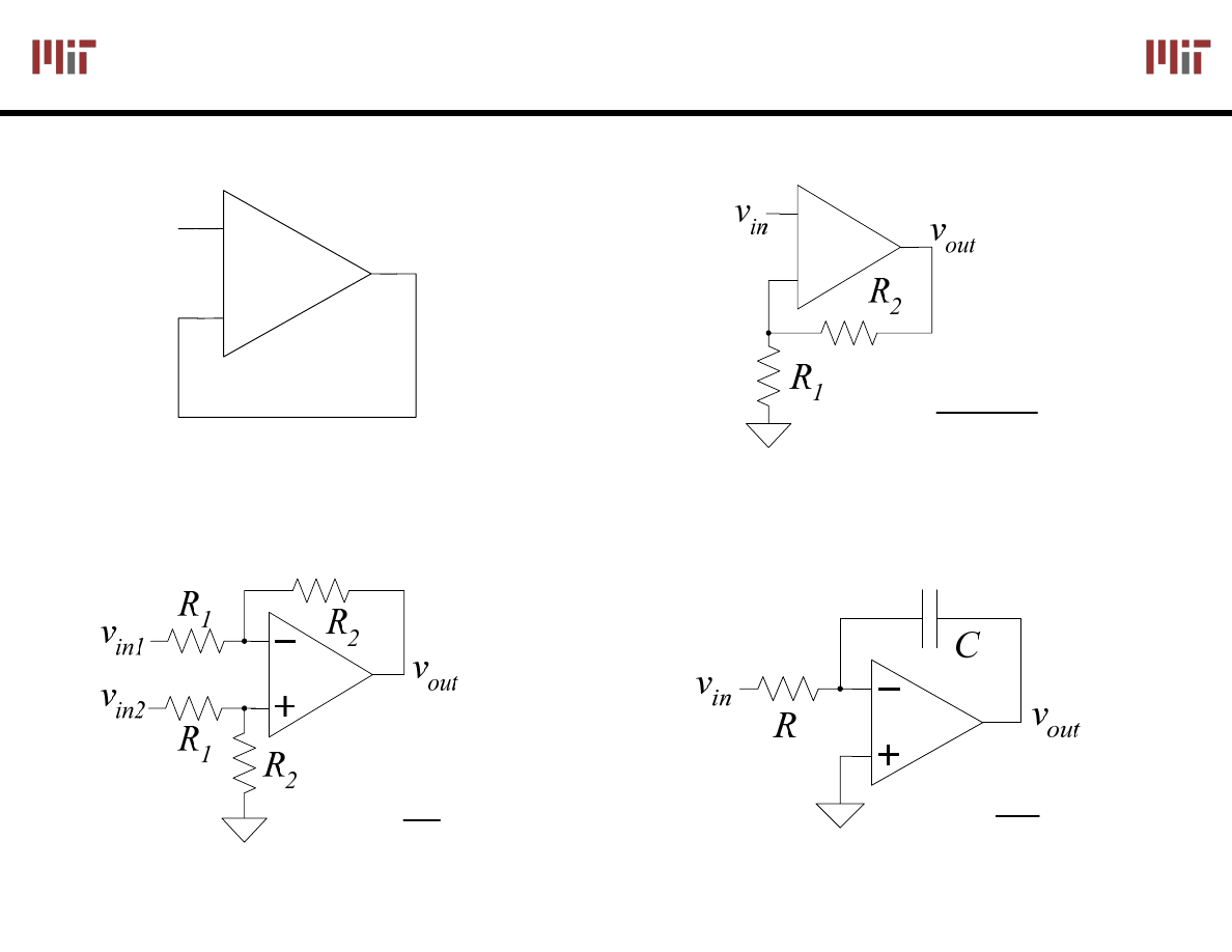
Basic
Basic
OpAmp
OpAmp
Circuits
Circuits
+
−
Voltage Follower (buffer)
Non-inverting
Differential Input
in
v
out
v
in
out
v
v
≈
Integrator
+
-
in
out
v
R
R
R
v
1
2
1
+
≈
(
)
1
2
1
2
in
in
R
R
out
v
v
v
−
≈
dt
v
v
t
in
RC
out
∫
∞
−
−
≈
1
L10: 6.111 Spring 2006
7
Introductory Digital Systems Laboratory
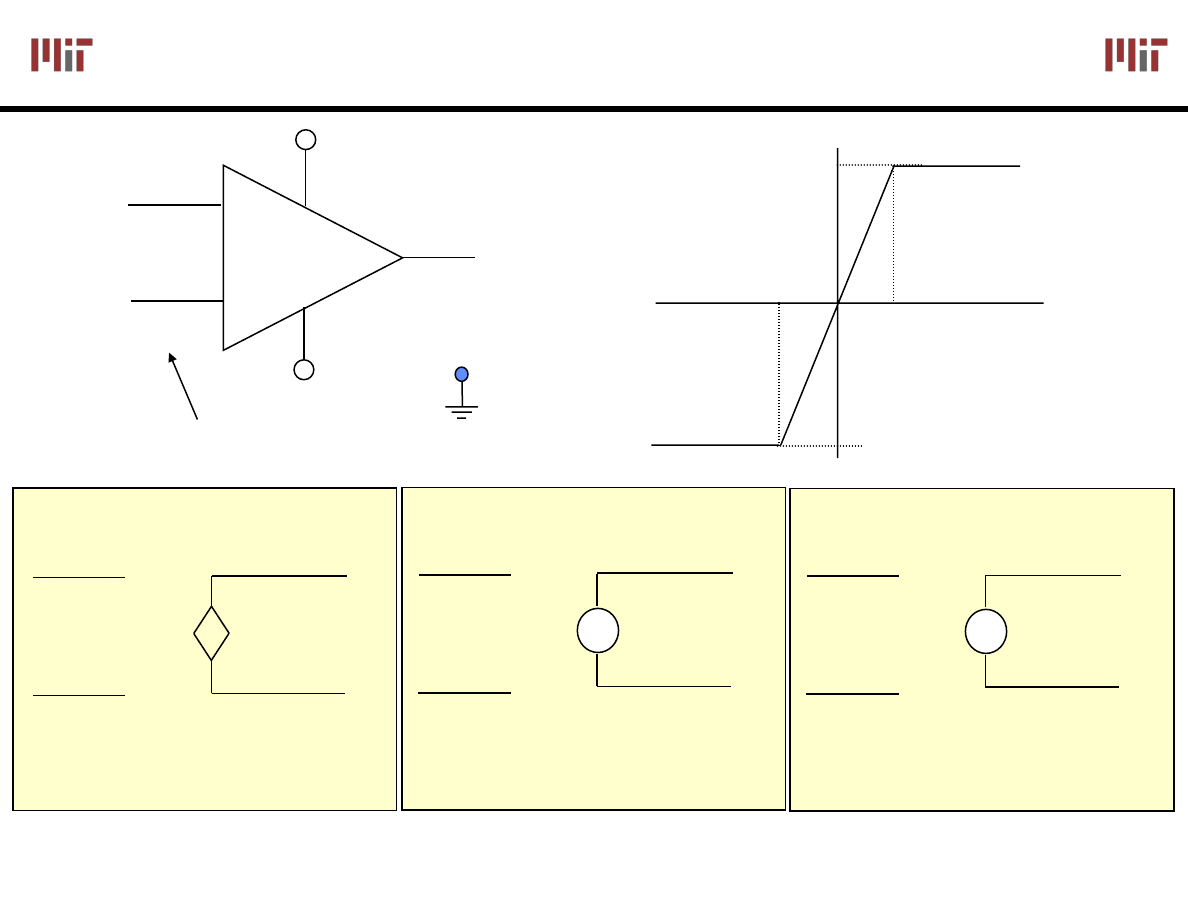
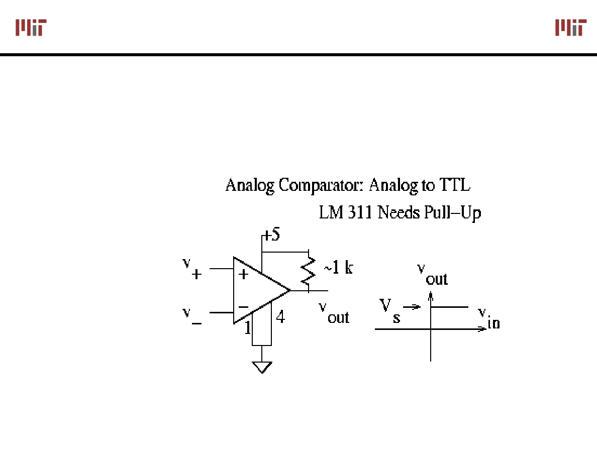
Use With Open Loop
Use With Open Loop
Analog Comparator:
Is V+ > V- ?
The Output is a DIGITAL signal
LM311 is a single supply
comparator
L10: 6.111 Spring 2006
8
Introductory Digital Systems Laboratory
Data Conversion: Quantization Noise
Data Conversion: Quantization Noise
Quantization noise exists even with
ideal
A/D and D/A converters
in
v
noise
v
LSB
A/D
D/A
digital
code
in
v
Quantization
noise
+
−
00 01 10 11
0
4
ref
V
2
ref
V
4
3
ref
V
Binary code
A
n
a
log O
u
tp
ut
00
01
10
11
0
4
ref
V
2
ref
V
4
3
ref
V
Analog Input
B
in
a
ry
O
u
tp
u
t
ref
V
4
ref
V
2
ref
V
4
3
ref
V
ref
V
A/D Conversion
D/A Conversion
L10: 6.111 Spring 2006
9
Introductory Digital Systems Laboratory
Non
Non
-
-
idealities in Data Conversion
idealities in Data Conversion
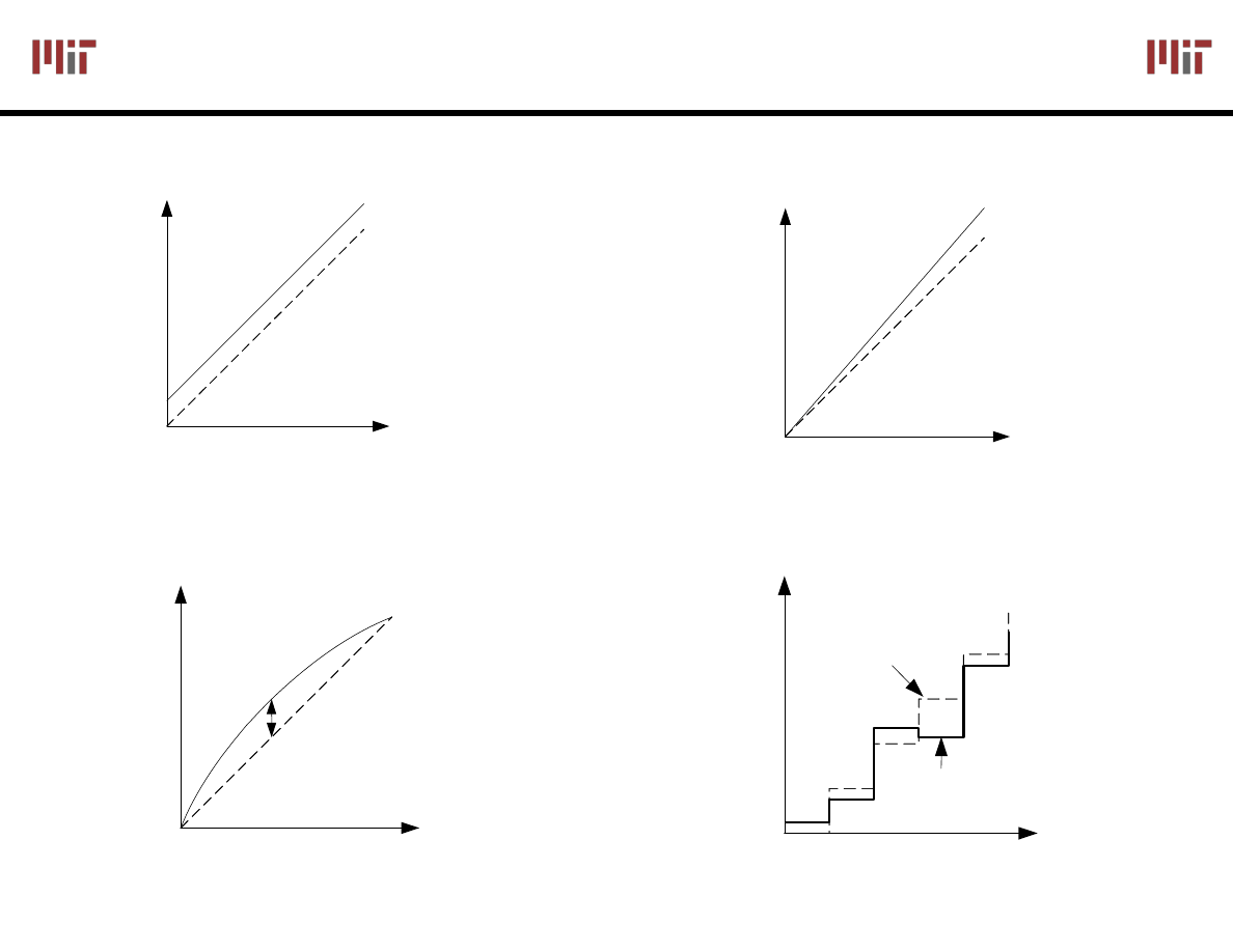
Binary code
A
nal
o
g
Ideal
Offset
error
Binary code
A
n
al
og
Ideal
Gain
error
Offset
– a constant voltage offset that appears
at the output when the digital input is 0
Gain error
– deviation of slope from ideal value
of 1
Binary code
A
nal
og
Ideal
Integral
nonlinearity
Integral Nonlinearity
– maximum deviation from
the ideal analog output voltage
Differential nonlinearity
– the largest increment
in analog output for a 1-bit change
Binary code
An
a
lo
g
Ideal
Non-
monoticity
L10: 6.111 Spring 2006
10
Introductory Digital Systems Laboratory
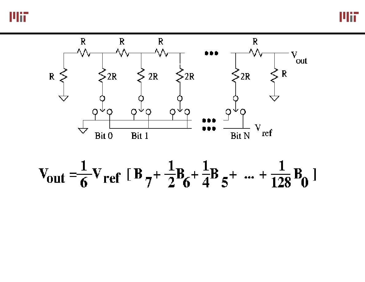
R
R
-
-
2R Ladder DAC Architecture
2R Ladder DAC Architecture
Note that the driving point impedance (resistance) is the same
for each cell.
R-2R Ladder achieves large current division ratios with only
two resistor values
-1
L10: 6.111 Spring 2006
Introductory Digital Systems Laboratory
11
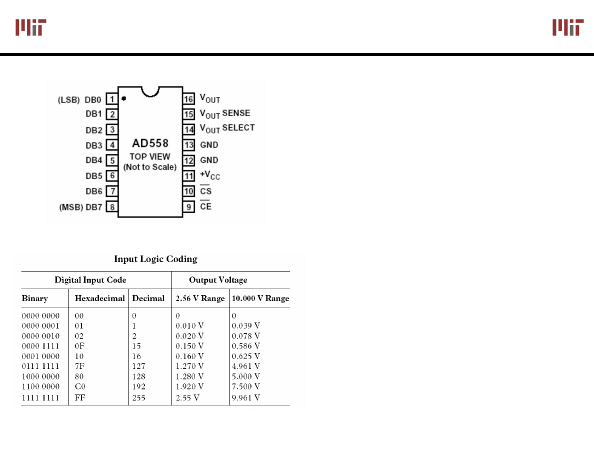
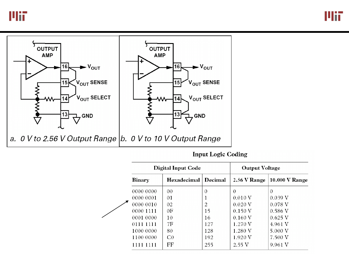
8-bit DAC
Single Supply Operation: 5V to 15V
Integrates required references
(bandgap voltage reference)
Uses a R-2R resistor ladder
Settling time 1
μs
Programmable output range from
0V to 2.56V or 0V to 10V
Simple Latch based interface
Image courtesy of Analog Devices. Used with permission.
DAC (AD 558) Specs
DAC (AD 558) Specs
L10: 6.111 Spring 2006
12
Introductory Digital Systems Laboratory
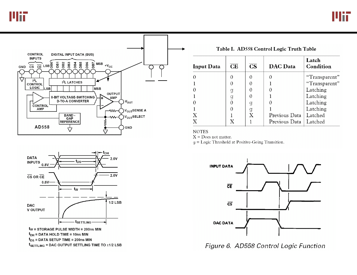
Chip Architecture and Interface
Chip Architecture and Interface
CE
CS
LATCH
D[7:0]
Outputs are noisy
when input bits settles,
so it is best to have inputs
stable before latching
the input data
Image courtesy of Analog Devices. Used with permission.
L10: 6.111 Spring 2006
13
Introductory Digital Systems Laboratory
Setting the Voltage Range
Setting the Voltage Range
Very similar to a
non-inverting amp
Strap output for
different voltage
ranges
Convert data to
Offset binary
Image courtesy of Analog Devices. Used with permission.
L10: 6.111 Spring 2006
14
Introductory Digital Systems Laboratory
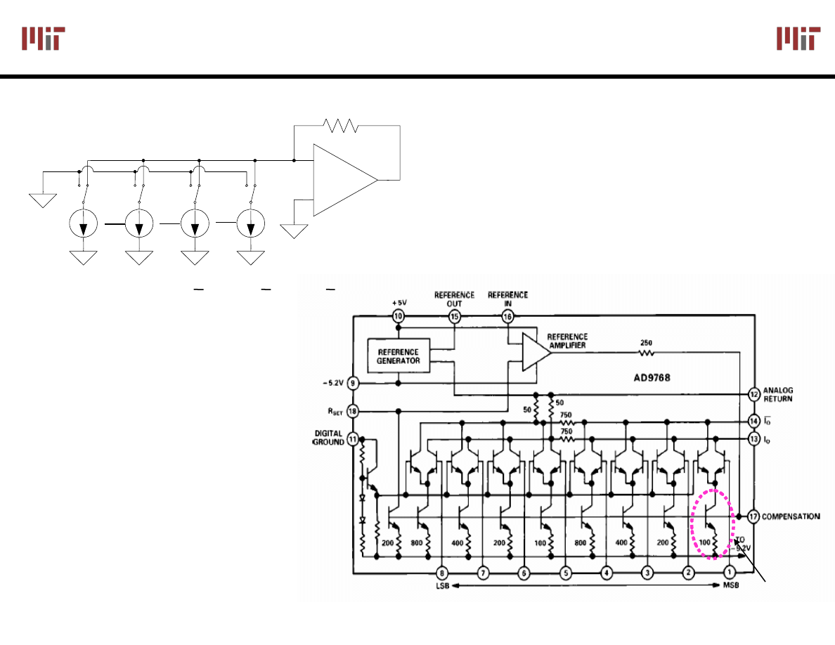
Another Approach: Binary
Another Approach: Binary
-
-
Weighted DAC
Weighted DAC
Analog Devices AD9768
uses two banks of
ratioed currents
Additional current
division performed by
750 Ω resistor between
the two banks
Switch binary-weighted
currents
MSB to LSB current ratio is 2
N
AD9768
3
b
2
b
1
b
0
b
R
out
v
(
)
0
8
1
1
4
1
2
2
1
3
b
b
b
b
IR
v
out
+
+
+
−
=
+
-
I
2
I
I
4
I
8
Reference current source
Image courtesy of Analog Devices. Used with permission.
L10: 6.111 Spring 2006
15
Introductory Digital Systems Laboratory
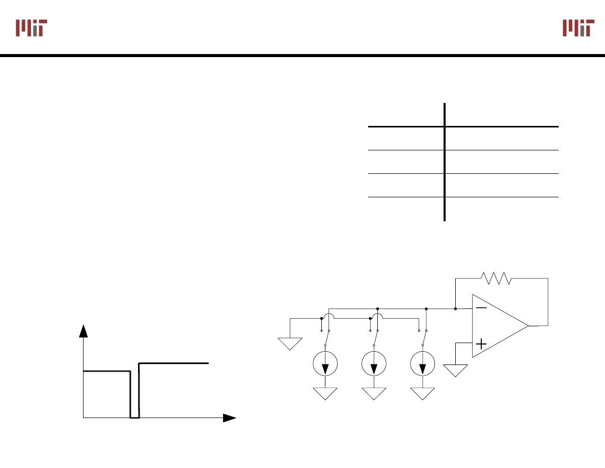
Glitching
Glitching
and Thermometer D/A
and Thermometer D/A
Glitching is caused when
switching times in a D/A are not
synchronized
Example: Output changes from
011 to 100 – MSB switch is
delayed
Filtering reduces glitch but
increases the D/A settling time
One solution is a thermometer
code D/A – requires 2
N
– 1
switches but no ratioed
currents
100
011→
out
v
t
Binary
Thermometer
0
0
0
0
0
0
1
0
0
1
1
0
0
1
1
1
1
1
1
1
0
T
I
R
out
v
(
)
2
1
0
T
T
T
IR
v
out
+
+
−
=
I
I
1
T
2
T
L10: 6.111 Spring 2006
16
Introductory Digital Systems Laboratory
Successive
Successive
-
-
Approximation A/D
Approximation A/D
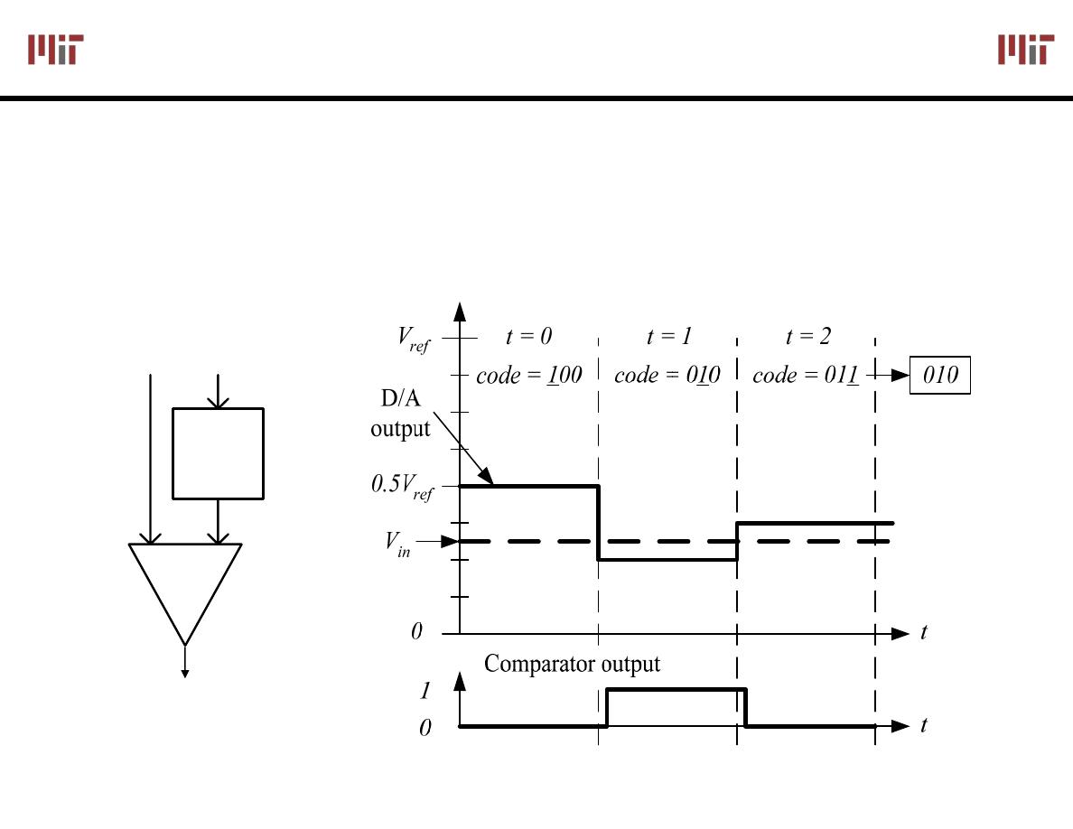
Example: 3-bit A/D conversion, 2 LSB < V
in
< 3 LSB
D/A converters are typically compact and easier to design. Why not A/D convert
using a D/A converter and a comparator?
D to A generates analog voltage which is compared to the input voltage
If D to A voltage > input voltage then set that bit; otherwise, reset that bit
This type of A to D takes a fixed amount of time proportional to the bit length
V
in
code
D/A
Comparator
out
C
+ −
L10: 6.111 Spring 2006
17
Introductory Digital Systems Laboratory
Successive
Successive
-
-
Approximation A/D
Approximation A/D
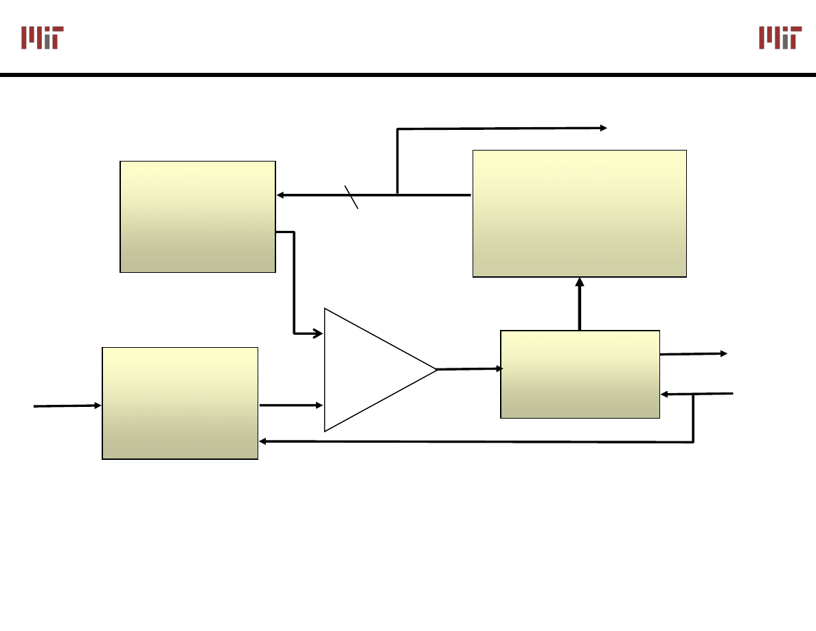
Serial conversion takes a time equal to N(t
D/A
+ t
comp
)
Successive
Approximation
Generator
Control
Done
Go
-
+
Sample/
Hold
D/A
Converter
v
in
N
Data
L10: 6.111 Spring 2006
18
Introductory Digital Systems Laboratory
Successive
Successive
-
-
Approximation A/D
Approximation A/D
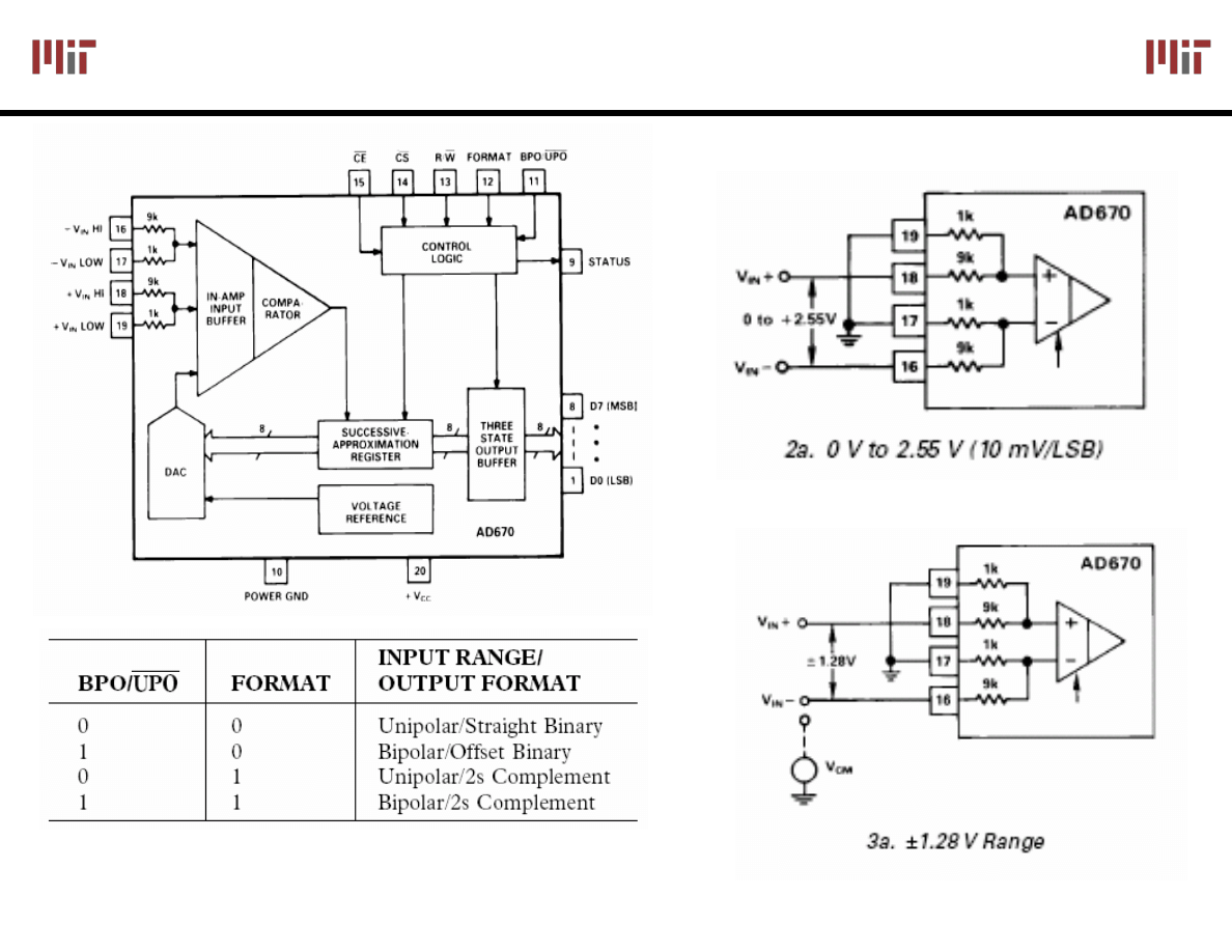
(AD670)
(AD670)
~10μs conversion time
Unipolar (BPO =0)
Bipolar (BPO =1)
Image courtesy of Analog Devices. Used with permission.
L10: 6.111 Spring 2006
19
Introductory Digital Systems Laboratory
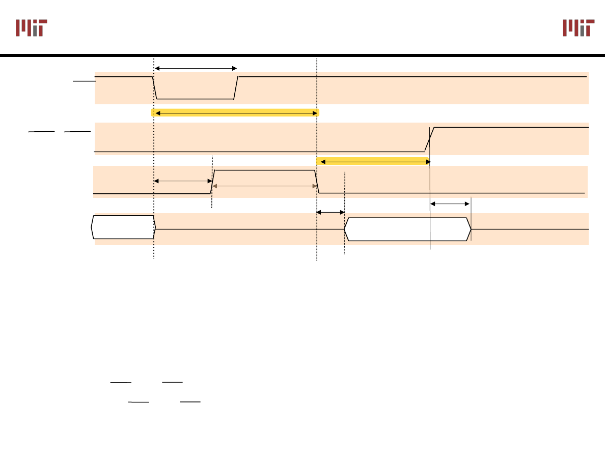
Single Write, Single Read Operation
Single Write, Single Read Operation
(see data sheet for other modes)
(see data sheet for other modes)
R/W
CE, CS
Data
Data Valid
t
w
Valid
t
DC
t
w
(write/start pulse width) = 300ns (min)
t
DC
(delay to start conversion) = 700ns (max)
t
c
(conversion time) = 10
μs (max)
t
TD
(Bus Access Time) = 250 (max)
t
DT
(Output Float Delay) = 150 (max)
t
c
t
TD
t
DT
Write
Read
Control bits CE and CS can be wired to ground if A/D is the only chip driving the bus
Suggestion: tie CE and CS pins together and hardwire BPO and Format
Status
L10: 6.111 Spring 2006
20
Introductory Digital Systems Laboratory
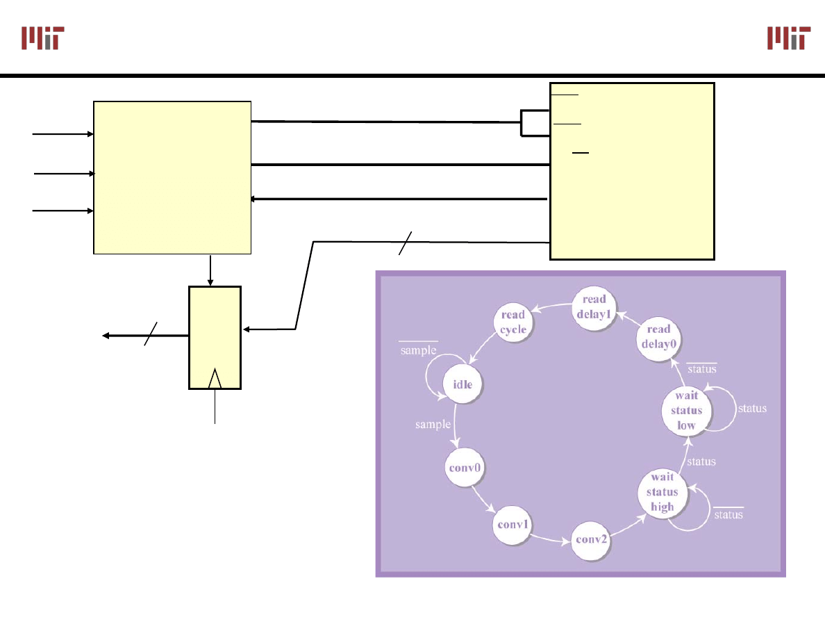
Simple A/D Interface FSM
Simple A/D Interface FSM
Data[7:0]
STATUS
CS
CE
AD670
cs_b
R/W
r_w_b
FSM
clk
reset
sample
D
Q
dataavail
status
Status should be
synchronized: why?
Courtesy of James Oey and
Cemal Akcaba
Figure by MIT OpenCourseWare.

L10: 6.111 Spring 2006
21
Introductory Digital Systems Laboratory
2/5
Example A/D
Example A/D
Verilog
Verilog
Interface
Interface
module AD670 (clk, reset, sample, dataavail,
r_wbar, cs_bar, status, state);
// System Clk
input clk;
// Global Reset signal, assume it is synchronized
input reset;
// User Interface
input sample;
output dataavail;
// A-D Interface
input status;
reg status_d1, status_d2;
output r_wbar, cs_bar;
output [3:0] state;
// internal state
reg [3:0] state;
reg [3:0] nextstate;
reg r_wbar_int, r_wbar;
reg cs_bar_int, cs_bar;
reg dataavail;
1/5
// State declarations.
parameter IDLE = 0;
parameter CONV0 = 1;
parameter CONV1 = 2;
parameter CONV2 = 3;
parameter WAITSTATUSHIGH = 4;
parameter WAITSTATUSLOW = 5;
parameter READDELAY0 = 6;
parameter READDELAY1 = 7;
parameter READCYCLE = 8;
always @ (posedge clk or negedge reset)
begin
if (!reset) state <=IDLE;
else state <=nextstate;
status_d1 <= status;
status_d2 <= status_d1;
r_wbar <= r_wbar_int;
cs_bar <=cs_bar_int;
end

L10: 6.111 Spring 2006
22
Introductory Digital Systems Laboratory
3/5
Example A/D
Example A/D
Verilog
Verilog
Interface (cont.)
Interface (cont.)
always @ (state or status_d2 or sample) begin
// defaults
r_wbar_int = 1; cs_bar_int = 1; dataavail = 0;
case (state)
IDLE: begin
if(sample) nextstate = CONV0;
else nextstate = IDLE;
end
CONV0:
begin
r_wbar_int = 0;
cs_bar_int = 0;
nextstate = CONV1;
end
CONV1:
begin
r_wbar_int = 0;
cs_bar_int = 0;
nextstate = CONV2;
end
CONV2:
begin
r_wbar_int = 0;
cs_bar_int = 0;
nextstate = WAITSTATUSHIGH;
end
WAITSTATUSHIGH:
begin
cs_bar_int = 0;
if (status_d2) nextstate = WAITSTATUSLOW;
else nextstate = WAITSTATUSHIGH;
end
WAITSTATUSLOW:
begin
cs_bar_int = 0;
if (!status_d2) nextstate = READDELAY0;
else nextstate = WAITSTATUSLOW;
end
4/5

L10: 6.111 Spring 2006
23
Introductory Digital Systems Laboratory
Example A/D
Example A/D
Verilog
Verilog
Interface(cont
Interface(cont
.)
.)
READDELAY0:
begin
cs_bar_int = 0;
nextstate = READDELAY1;
end
READDELAY1:
begin
cs_bar_int = 0;
nextstate = READCYCLE;
end
READCYCLE:
begin
cs_bar_int = 0;
dataavail = 1;
nextstate = IDLE;
end
default: nextstate = IDLE;
endcase // case(state)
end // always @ (state or status_d2 or sample)
endmodule // adcInterface
5/5
L10: 6.111 Spring 2006
24
Introductory Digital Systems Laboratory
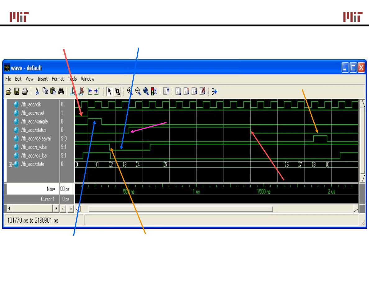
Simulation
Simulation
On reset, present state goes to 0
Sample pulse initiates
data conversion
Notice a one cycle delay since A/D
control signal delayed through a register
r_w_b must stay low for at least 3 cycles (@ 100ns period)
Status is synchronized – two register delays
Wait for ~10
μs for status to go low
Enable read flip-flop
L10: 6.111 Spring 2006
25
Introductory Digital Systems Laboratory
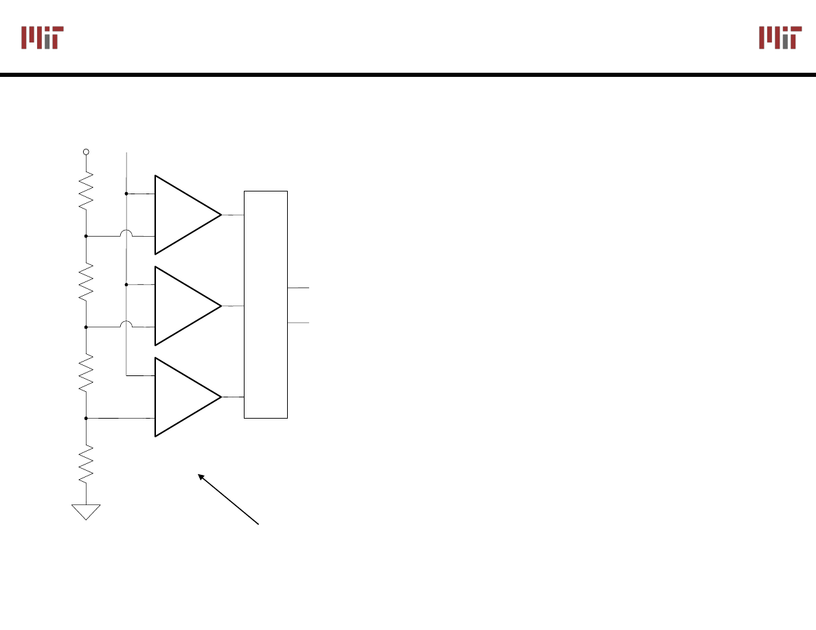
Flash A/D Converter
Flash A/D Converter
Brute-force A/D conversion
Simultaneously compare the
analog value with every
possible reference value
Fastest method of A/D
conversion
Size scales exponentially
with precision
(requires 2
N
comparators)
C
+
−
C
+
−
C
+
−
R
R
ref
V
in
v
0
b
1
b
Th
e
rmo
m
e
ter
to
b
in
a
ry
Comparators
R
R
Can be implemented as OpAmp in open loop
L10: 6.111 Spring 2006
26
Introductory Digital Systems Laboratory
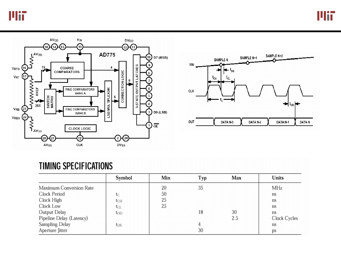
AD 775
AD 775
–
–
Flash Data Converter
Flash Data Converter
Image courtesy of Analog Devices. Used with permission.
L10: 6.111 Spring 2006
27
Introductory Digital Systems Laboratory
Amplifier
Amplifier
−
−
Sample/
A/D
D/A
Sample/
A/D
D/A
…
2
2
Hold
Converter
Converter
Hold
Converter
Converter
+
+
1-bit
1-bit
Pipelining (used in video rate, RF basestations, etc.)
Parallelism (use many slower A/D’s in parallel to build very
high speed A/D converters)
[ISSCC 2003],
Poulton et. al.
20Gsample/sec,
8-bit ADC
from Agilent Labs
Figure by MIT OpenCourseWare. Adapted from Poulten, Ken, et al. "A 20 GS/s 8b ADC with a 1MB Memory in 0.18um CMOS."
IEEE International Solid-State Circuits Conference Paper 18.1, 2003.
DLL
1 GHz
Clock
Clock
Gen
CMOS
Buffer Chip
2 muxes
80
T/Hs and
V/Is
80
ADC Slices
80 Radix Converters
80 Slice Decimator
8 Mem Controllers
1MByte SRAM
0.18- CMOS ADC Chip
High Performance Converters:
High Performance Converters:
Use Pipelining and Parallelism!
Use Pipelining and Parallelism!

L10: 6.111 Spring 2006
28
Introductory Digital Systems Laboratory
New Trend: Eliminate
New Trend: Eliminate
OpAmps
OpAmps
!
!
(Use Comparators, more digital
(Use Comparators, more digital
…
…
)
)
Op amps must achieve high
open-loop gain and fast
settling time under
feedback.
High gain becomes
increasingly difficult
achieve due to low device
gain.
Solution: Comparator
based analog Design
Dramatic power savings
possible
Courtesy of Prof. Harry Lee, ISSCC 2006. Used with permission.

L10: 6.111 Spring 2006
29
Introductory Digital Systems Laboratory
Summary of Analog Blocks
Summary of Analog Blocks
Analog blocks are integral components of any
system. Need data converters (analog to digital
and digital to analog), analog processing
(OpAmps circuits, switched capacitors filters,
etc.), power converters (e.g., DC-DC
conversion), etc.
We looked at example interfaces for A/D and
D/A converters
Make sure you register critical signals (enables, R/W,
etc.)
Analog design incorporate digital principles
Glitch free operation using coding
Parallelism and Pipelining!
More advanced concepts such as calibration
Document Outline
- L10: Analog Building Blocks (OpAmps, A/D, D/A)
- Introduction to Operational Amplifiers
- The Inside of a 741 OpAmp
- Simple Model for an OpAmp
- The Power of (Negative) Feedback
- Basic OpAmp Circuits
- Use With Open Loop
- Data Conversion: Quantization Noise
- Non-idealities in Data Conversion
- R-2R Ladder DAC Architecture
- DAC (AD 558) Specs
- Chip Architecture and Interface
- Setting the Voltage Range
- Another Approach: Binary-Weighted DAC
- Glitching and Thermometer D/A
- Successive-Approximation A/D
- Successive-Approximation A/D
- Successive-Approximation A/D (AD670)
- Single Write, Single Read Operation (see data sheet for other modes)
- Simple A/D Interface FSM
- Example A/D Verilog Interface
- Example A/D Verilog Interface (cont.)
- Example A/D Verilog Interface(cont.)
- Simulation
- Flash A/D Converter
- AD 775 – Flash Data Converter
- High Performance Converters: Use Pipelining and Parallelism!
- Summary of Analog Blocks
Wyszukiwarka
Podobne podstrony:
Projektowanie analogowych układów scalonych
19 zapis binarny systemow analogowych
Principles of Sigma Delta Conversion for Analog to Digital Converters
Narządy analogiczne i homologiczne
Applications of polyphase filters for bandpass sigma delta analog to digital conversion
10 Programowa obsługa sygnałów analogowych materiały wykładowe
4Regulatory analogowe
9 PRZETWORNIKI ANOLOGOWO CYFROWE ORAZ CYFROWO ANALOGOWE
K4 L10
Analogie s owne(2)
Elektronika analogowa czym mierzyc
Instalacja analogowego tunera
Moje usługi dodatkowe DLA TELEFONII ANALOGOWEI OFEROWANE W SYSTEMIE CENTRAL CYFROWYCH (2)
analogi
Elektrotechnika i elektronika analogowa
PLL analogi
więcej podobnych podstron