HCC/HCF4093B
QUAD 2-INPUT NAND SCHMIDT TRIGGERS
.
SCHMITT-TRIGGER ACTION ON EACH INPUT
WITH NO EXTERNAL COMPONENTS
.
HYSTERESIS VOLTAGE TYPICALLY 0.9V AT
V
DD
= 5V AND 2.3V AT V
DD
= 10V
.
NOISE IMMUNITY GREATER THAN 50% OF
V
DD
(typ.)
.
NO LIMIT ON INPUT RISE AND FALL TIMES
.
STANDARDIZED
SYMMETRICAL
OUTPUT
CHARACTERISTICS
.
QUIESCENT CURRENT SPECIFIED TO 20V
FOR HCC DEVICE
.
5V, 10V, AND 15V PARAMETRIC RATINGS
.
INPUT CURRENT OF 100nA AT 18V AND
25
°
C FOR HCC DEVICE
.
100% TESTED FOR QUIESCENT CURRENT
.
MEETS ALL REQUIREMENTS OF JEDEC TEN-
TATIVE STANDARD N
°
. 13A, ”STANDARD
SPECIFICATIONS FOR DESCRIPTION OF ”B”
SERIES CMOS DEVICES”
June 1989
EY
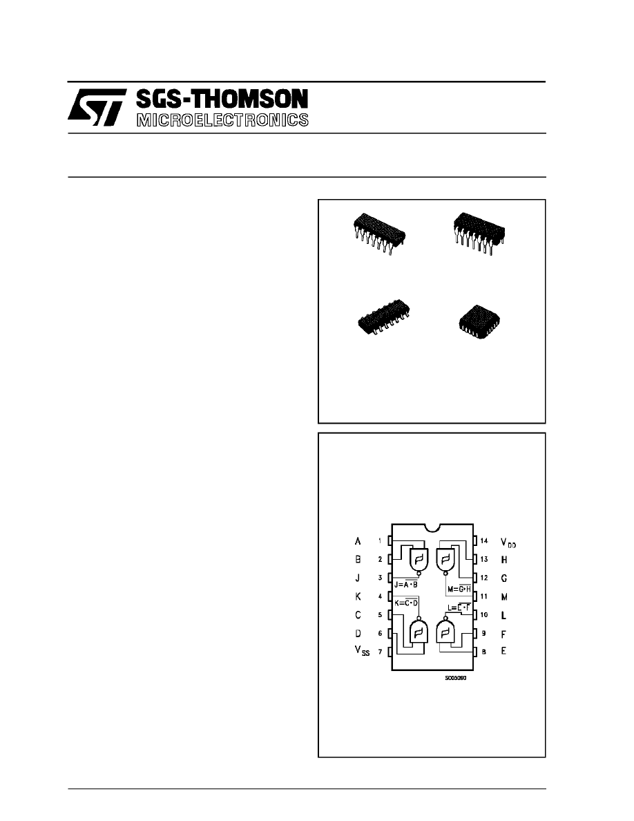
(Plastic Package)
F
(Ceramic Frit Seal Package)
C1
(Plastic Chip Carrier)
ORDER CODES :
HCC4093BF
HCF4093BM1
HCF4093BEY
HCF4093BC1
PIN CONNECTIONS
M1
(Micro Package)
DESCRIPTION
The HCC4093B (extended temperature range) and
HCF4093B (intermediate temperature range) are
available in 14-lead dual in-line plastic or ceramic
package
and
plastic
micropackage.
The
HCC/HCF4093B consists of four Schmitt-trigger cir-
cuits. Each circuit functions as a two-input NAND
gate with Schmitt-trigger action on both inputs. The
gate switches at different points for positive and ne-
gative-going signals.
The difference between the positive voltage (V
P
)
and the negative voltage (V
N
) is defined as hys-
teresis voltage (V
H
) (see fig. 1).
1/13
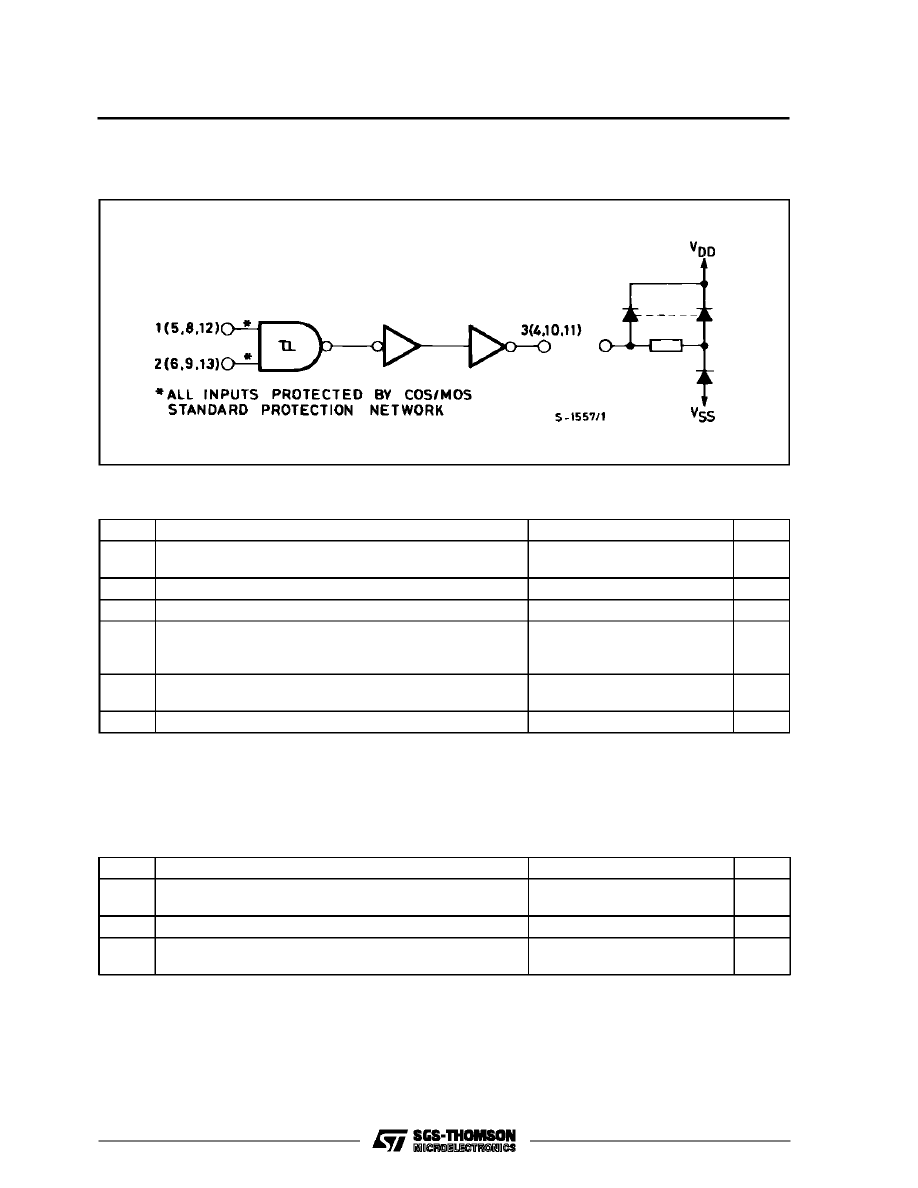
FUNCTIONAL DIAGRAM
ABSOLUTE MAXIMUM RATINGS
Symbol
Parameter
Value
Unit
V
DD
*
Supply Voltage : HC C Types
H C F Types
– 0.5 to + 20
– 0.5 to + 18
V
V
V
I
Input Voltage
– 0.5 to V
DD
+ 0.5
V
I
I
DC Input Current (any one input)
±
10
mA
P
t o t
Total Power Dissipation (per package)
Dissipation per Output Transistor
for T
o p
= Full Package-temperature Range
200
100
mW
mW
T
o p
Operating Temperature : HCC Types
H CF Types
– 55 to + 125
– 40 to + 85
°
C
°
C
T
s t g
Storage Temperature
– 65 to + 150
°
C
RECOMMENDED OPERATING CONDITIONS
Symbol
Parameter
Value
Unit
V
DD
Supply Voltage : HC C Types
H CF Types
3 to 18
3 to 15
V
V
V
I
Input Voltage
0 to V
DD
V
T
o p
Operating Temperature : HCC Types
H CF Types
– 55 to + 125
– 40 to + 85
°
C
°
C
Stresses above those listed under ”Absolute Maximum Ratings ”may cause permanent damage to the device. This is a stress
rating only and functional operation of the device at these or any other conditions above those indicated in the operational sec-
tions of this specifi cation is not implied. Exposure to absolute maximum rating conditions for external periods may affect device
reliability.
* All voltage values are referred to V
SS
pin voltage.
1 of 4 Schmitt triggers
HCC/HCF4093B
2/13
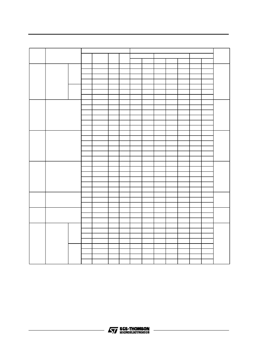
STATIC ELECTRICAL CHARACTERISTICS (over recommended operating conditions)
Test Conditions
Value
V
I
V
O
|I
O
|
V
D D
T
L o w
*
25
°
C
T
Hi g h
*
Symbol
Parameter
(V)
(V)
(
µ
A)
(V)
Mi n. Max. Min. Typ. Max. Min. Max.
Unit
I
L
Quiescent
Current
HCC
Types
0/ 5
5
1
0.02
1
30
µ
A
0/10
10
2
0.02
2
60
0/15
15
4
0.02
4
120
0/20
20
20
0.04
20
600
HCF
Types
0/ 5
5
4
0.02
4
30
0/10
10
8
0.02
8
60
0/15
15
16
0.02
16
120
V
P
Positive Trigger
Threshold Voltage
a
5
2.2
3.6
2.2
2.9
3.6
2.2
3.6
V
a
10
4.6
7.1
4.6
5.9
7.1
4.6
7.1
a
15
6.8
10.8
6.8
8.8
10.8
6.8
10.8
b
5
2.6
4
2.6
3.3
4
2.6
4
b
10
5.6
8.2
5.6
7
8.2
5.6
8.2
b
15
6.3
12.7
6.3
9.4
12.7
6.3
12.7
V
N
Negative Trigger
Threshold Voltage
a
5
0.9
2.8
0.9
1.9
2.8
0.9
2.8
V
a
10
2.5
5.2
2.5
3.9
5.2
2.5
5.2
a
15
4
7.4
4
5.8
7.4
4
7.4
b
5
1.4
3.2
1.4
2.3
3.2
1.4
3.2
b
10
3.4
6.6
3.4
5.1
6.6
3.4
6.6
b
15
4.8
9.6
4.8
7.3
9.6
4.8
9.6
V
H
Hysteresis Voltage
a
5
0.3
1.6
0.3
0.9
1.6
0.3
1.6
V
a
10
1.2
3.4
1.2
2.3
3.4
1.2
3.4
a
15
1.6
5
1.6
3.5
5
1.6
5
b
5
0.3
1.6
0.3
0.9
1.6
0.3
1.6
b
10
1.2
3.4
1.2
2.3
3.4
1.2
3.4
b
15
1.6
5
1.6
3.5
5
1.6
5
V
O H
Output High
Voltage
0/ 5
< 1
5
4.95
4.95
4.95
V
0/10
< 1
10
9.95
9.95
9.95
0/15
< 1
15
14.95
14.95
14.95
V
O L
Output Low
Voltage
5/0
< 1
5
0.05
0.05
0.05
V
10/0
< 1
10
0.05
0.05
0.05
15/0
< 1
15
0.05
0.05
0.05
I
O H
Output
Drive
Current
HCC
Types
0/ 5
2.5
5
– 2
– 1.6 – 3.2
– 1.15
mA
0/ 5
4.6
5
– 0.64
– 0.51 – 1
– 0.36
0/10
9.5
10
– 1.6
– 1.3 – 2.6
– 0.9
0/15
13.5
15
– 4.2
– 3.4 – 6.8
– 2.4
HCF
Types
0/ 5
2.5
5
– 1.53
– 1.36 – 3.2
– 1.1
0/ 5
4.6
5
– 0.52
– 0.44 – 1
– 0.36
0/10
9.5
10
– 1.3
– 1.1 – 2.6
– 0.9
0/15
13.5
15
– 3.6
– 3.0 – 6.8
– 2.4
a : input on terminals 1, 5, 8, 12 or 2, 6, 9, 13 ; other inputs to V
DD
.
b : input on terminals 1 and 2, 5 and 6, 8 and 9, or 12 and 13 ; other inputs to V
DD
.
* T
Lo w
= –55
°
C for HCC device : -40
°
C for HCF device.
* T
High
= +125
°
C for HCC device : +85
°
C for HCF device.
HCC/HCF4093B
3/13
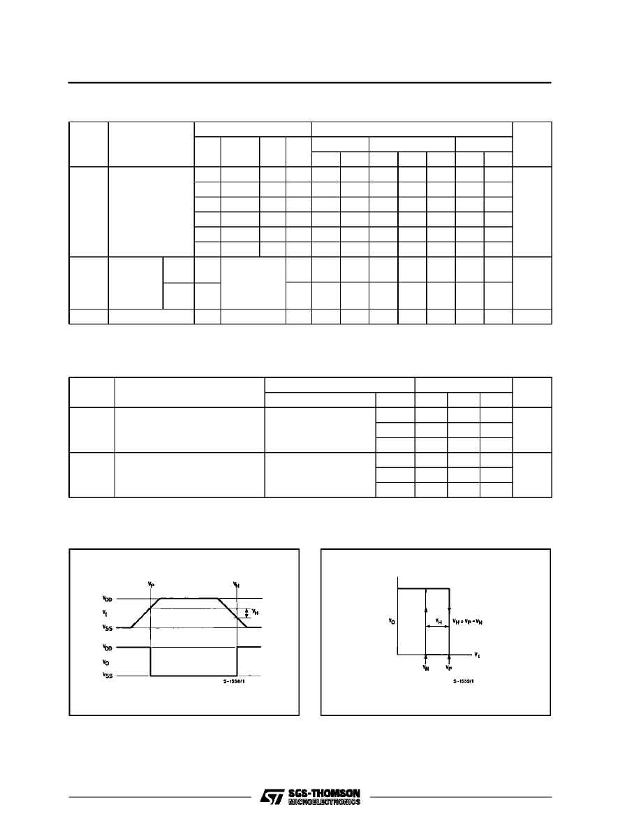
STATIC ELECTRICAL CHARACTERISTICS ( continued)
Test Conditions
Value
V
I
V
O
|I
O
|
V
D D
T
L o w
*
25
°
C
T
Hi g h
*
Symbol
Parameter
(V)
(V)
(
µ
A)
(V)
Min. Max. Min. Typ. Max. Min. Max.
Unit
I
O L
Output
Sink
Current
0/ 5
0.4
5
0.64
0.51
1
0.36
mA
0/10
0.5
10
1.6
1.3
2.6
0.9
0/15
1.5
15
4.2
3.4
6.8
2.4
0/ 5
0.4
5
0.52
0.44
1
0.36
0/10
0.5
10
1.3
1.1
2.6
0.9
0/15
1.5
15
3.6
3.0
6.8
2.4
I
IH
, I
IL
Input
Leakage
Current
HCC
Types
0/18
Any Input
µ
A
18
±
0.1
±
10
- 5
±
0.1
±
1
HCF
Types
0/15
15
±
0.3
±
10
-5
±
0.3
±
1
C
I
Input Capacitance
Any Input
5
7.5
pF
DYNAMIC ELECTRICAL CHARACTERISTICS (T
amb
= 25
°
C, C
L
= 50pF, R
L
= 200k
Ω
,
typical temperature coefficient for all V
DD
= 0.3%/
°
C values , all input rise and fall time = 20ns)
Val ue
Symbol
Parameter
Test Conditions
V
D D
(V)
Min.
Typ.
Max.
Unit
t
P L H
, t
P HL
Propagation Delay Time
5
190
380
ns
10
90
180
15
65
130
t
TL H
, t
T HL
Transition Time
5
100
200
ns
10
50
100
15
40
80
Figure1 : Hysteresis Definition, Characteristics and Test Setup.
(a) Definition of V
P
, V
N
and V
H
(b) Transfer characteristics of 1 of 4 gates
HCC/HCF4093B
4/13
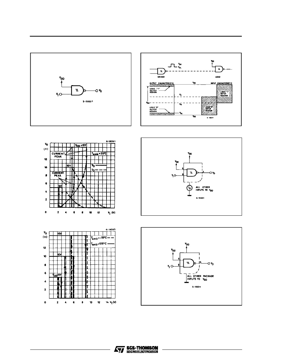
(c) Test setup
Figure 2 : Input and Output Characteristics.
Figure 3 : Typical Current and Voltage Transfer Characteristics.
Figure 4 : Typical Voltage Transfer Characteristics as a Function of Temperature, and Test Circuit.
HCC/HCF4093B
5/13
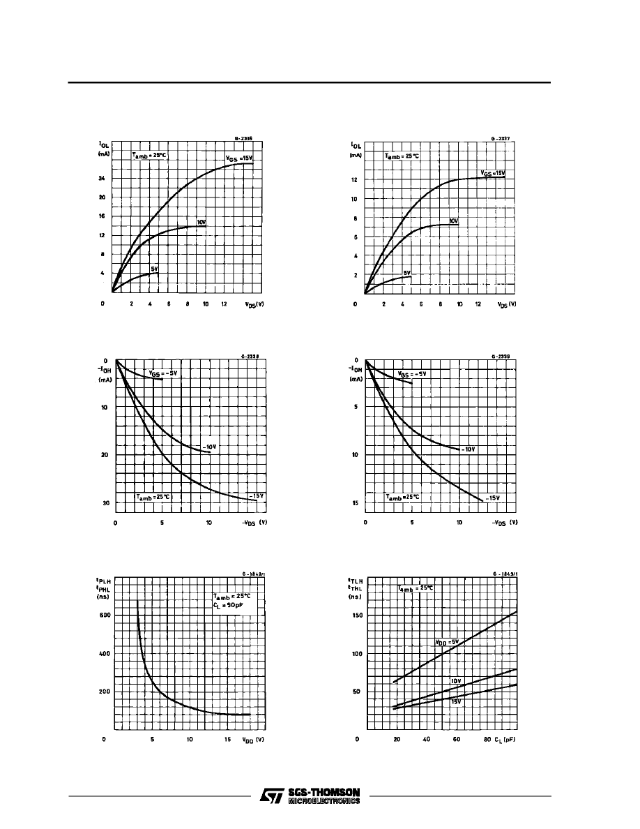
Figure 5 : Typical Output Low (sink) Current Char-
acteristics.
Figure 6 : Minimum Output Low (sink) Current Char-
acteristics.
Figure 7 : Typical Output High (source) Current
Characteristic.
Figure 8 : Minimum Output High Current Charac-
teristics.
Figure 9 : Typical Propagation Delay Time vs. Sup-
ply Voltage.
Figure 10 : Typical Transition Time vs. Load Capa-
citance.
HCC/HCF4093B
6/13
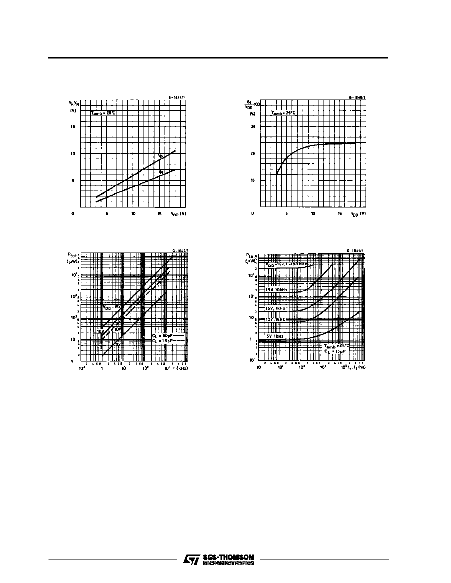
Figure 11 : Typical Trigger Threshold Voltage
vs.V
DD
Figure 12 : Typical per cent Hysteresis vs. Supply
Voltage.
Figure 13 : Typical Dissipation Characteristics.
Figure 14 : Power Dissipation vs. Rise and Fall
Times.
HCC/HCF4093B
7/13
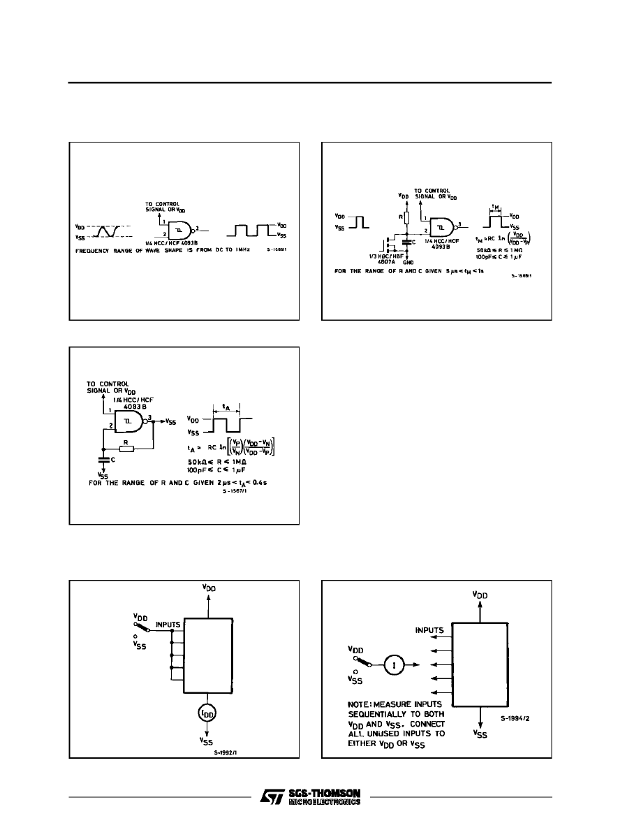
APPLICATIONS
Figure 15 : Wave Shaper.
Figure 16 : Monostable Multivibrator.
Figure17 : Astable Multivibrator.
Figure 19 : Input Leakage Current.
TEST CIRCUITS
Figure18 : Quiescent Device Current.
HCC/HCF4093B
8/13
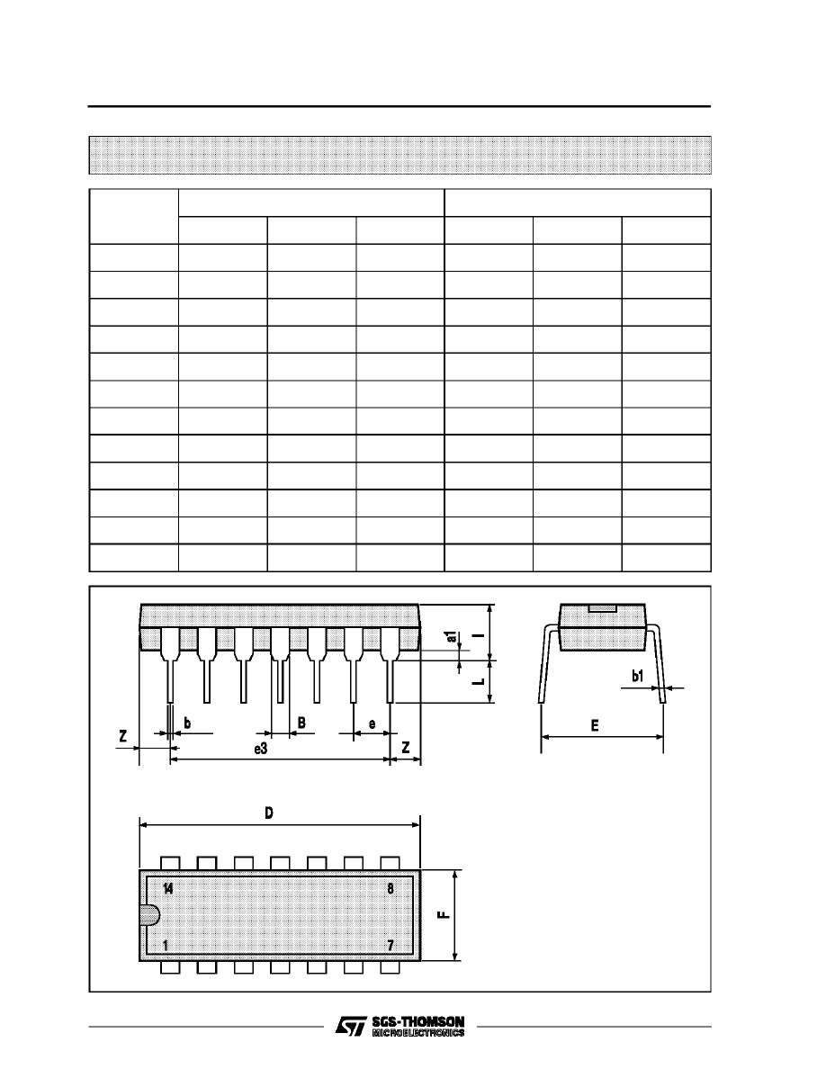
Plastic DIP14 MECHANICAL DATA
DIM.
mm
inch
MIN.
TYP.
MAX.
MIN.
TYP.
MAX.
a1
0.51
0.020
B
1.39
1.65
0.055
0.065
b
0.5
0.020
b1
0.25
0.010
D
20
0.787
E
8.5
0.335
e
2.54
0.100
e3
15.24
0.600
F
7.1
0.280
I
5.1
0.201
L
3.3
0.130
Z
1.27
2.54
0.050
0.100
P001A
HCC/HCF4093B
9/13
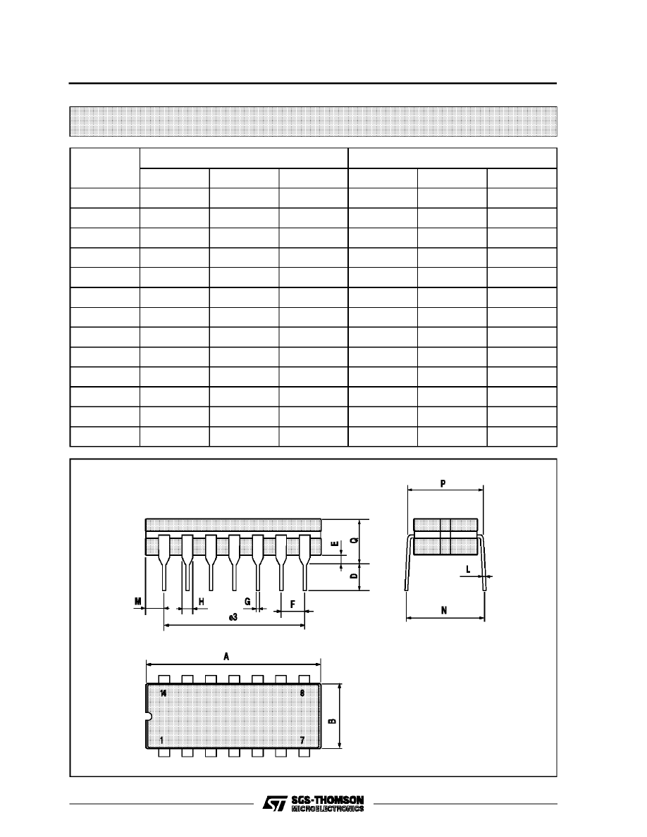
Ceramic DIP14/1 MECHANICAL DATA
DIM.
mm
inch
MIN.
TYP.
MAX.
MIN.
TYP.
MAX.
A
20
0.787
B
7.0
0.276
D
3.3
0.130
E
0.38
0.015
e3
15.24
0.600
F
2.29
2.79
0.090
0.110
G
0.4
0.55
0.016
0.022
H
1.17
1.52
0.046
0.060
L
0.22
0.31
0.009
0.012
M
1.52
2.54
0.060
0.100
N
10.3
0.406
P
7.8
8.05
0.307
0.317
Q
5.08
0.200
P053C
HCC/HCF4093B
10/13
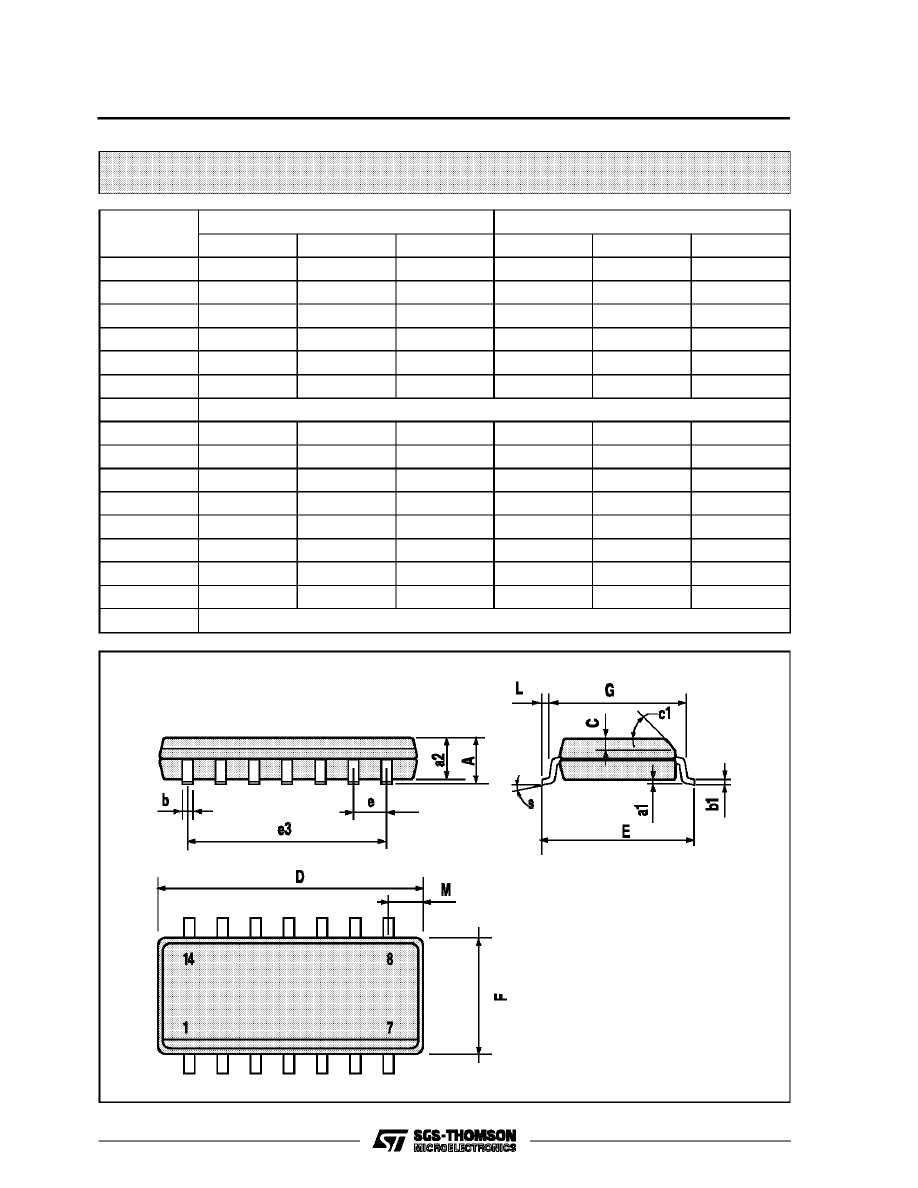
SO14 MECHANICAL DATA
DIM.
mm
inch
MIN.
TYP.
MAX.
MIN.
TYP.
MAX.
A
1.75
0.068
a1
0.1
0.2
0.003
0.007
a2
1.65
0.064
b
0.35
0.46
0.013
0.018
b1
0.19
0.25
0.007
0.010
C
0.5
0.019
c1
45
°
(typ.)
D
8.55
8.75
0.336
0.344
E
5.8
6.2
0.228
0.244
e
1.27
0.050
e3
7.62
0.300
F
3.8
4.0
0.149
0.157
G
4.6
5.3
0.181
0.208
L
0.5
1.27
0.019
0.050
M
0.68
0.026
S
8
°
(max.)
P013G
HCC/HCF4093B
11/13
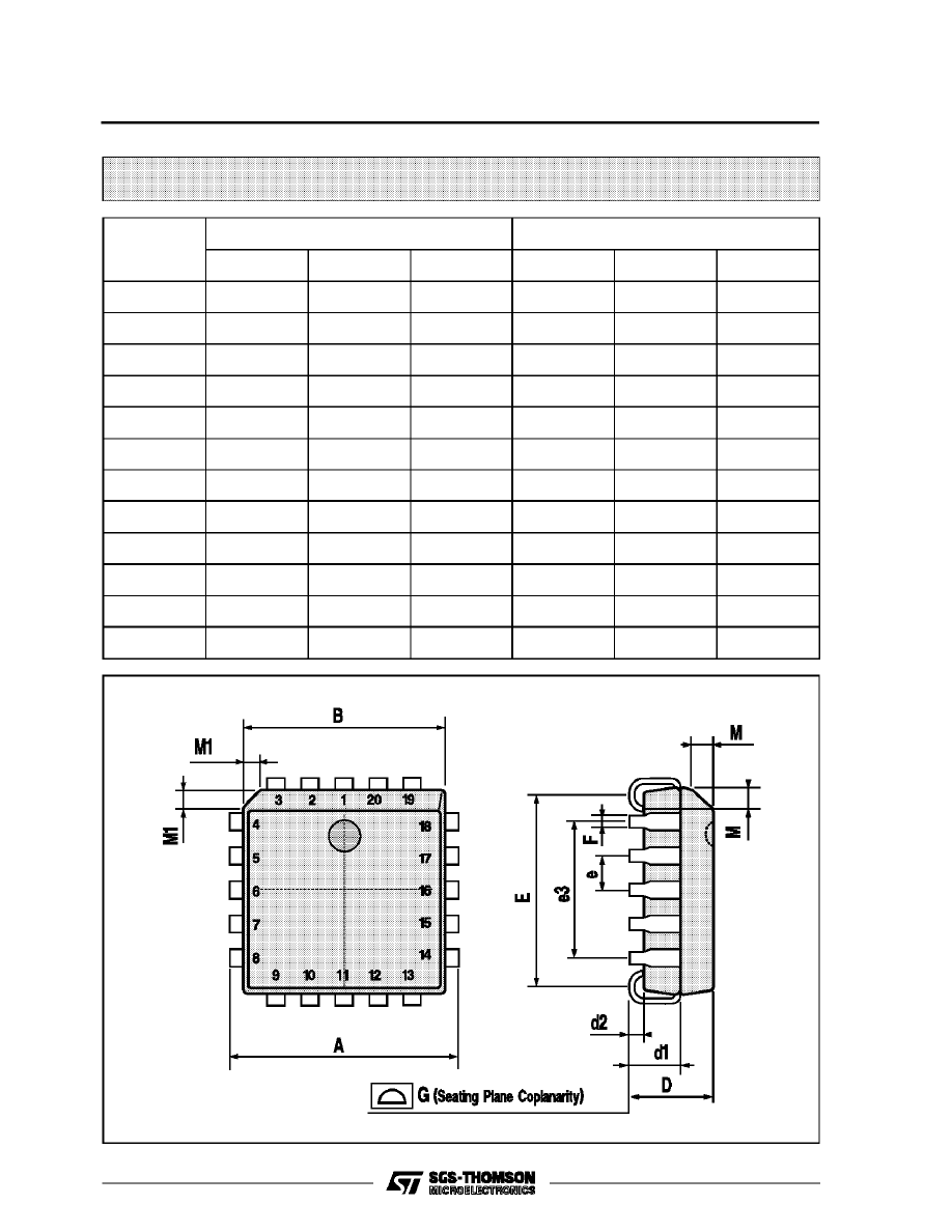
PLCC20 MECHANICAL DATA
DIM.
mm
inch
MIN.
TYP.
MAX.
MIN.
TYP.
MAX.
A
9.78
10.03
0.385
0.395
B
8.89
9.04
0.350
0.356
D
4.2
4.57
0.165
0.180
d1
2.54
0.100
d2
0.56
0.022
E
7.37
8.38
0.290
0.330
e
1.27
0.050
e3
5.08
0.200
F
0.38
0.015
G
0.101
0.004
M
1.27
0.050
M1
1.14
0.045
P027A
HCC/HCF4093B
12/13
Information furnished is believed to be accurate and reliable. However, SGS-THOMSON Microelectronics assumes no responsability for the
consequences of use of such information nor for any infringement of patents or other rights of third parties which may results from its use. No
license is granted by implication or otherwise under any patent or patent rights of SGS-THOMSON Microelectronics. Specifications mentioned
in this publication are subject to change without notice. This publication supersedes and replaces all information previously supplied.
SGS-THOMSON Microelectronics products are not authorized for use as critical components in life support devices or systems without express
written approval of SGS-THOMSON Microelectonics.
1994 SGS-THOMSON Microelectronics - All Rights Reserved
SGS-THOMSON Microelectronics GROUP OF COMPANIES
Australia - Brazil - France - Germany - Hong Kong - Italy - Japan - Korea - Malaysia - Malta - Morocco - The Netherlands -
Singapore - Spain - Sweden - Switzerland - Taiwan - Thailand - United Kingdom - U.S.A
HCC/HCF4093B
13/13
Wyszukiwarka
Podobne podstrony:
4093
4093
4093
4093
4093
więcej podobnych podstron