
Jin-Fu Li
Department of Electrical Engineering
National Central University
Jungli, Taiwan
Chapter 4
Chapter 4
ARM Instruction Sets
ARM Instruction Sets

Advanced Reliable Systems (ARES) Lab.
Jin-Fu Li, EE, NCU
2
¾
Registers, Memory Access, and Data Transfer
¾
Arithmetic and Logic Instructions
¾
Branch Instructions
¾
Assembly Language
¾
I/O Operations
¾
Subroutines
¾
Program Examples
Outline
Advanced Reliable Systems (ARES) Lab.
Jin-Fu Li, EE, NCU
3
Content Coverage
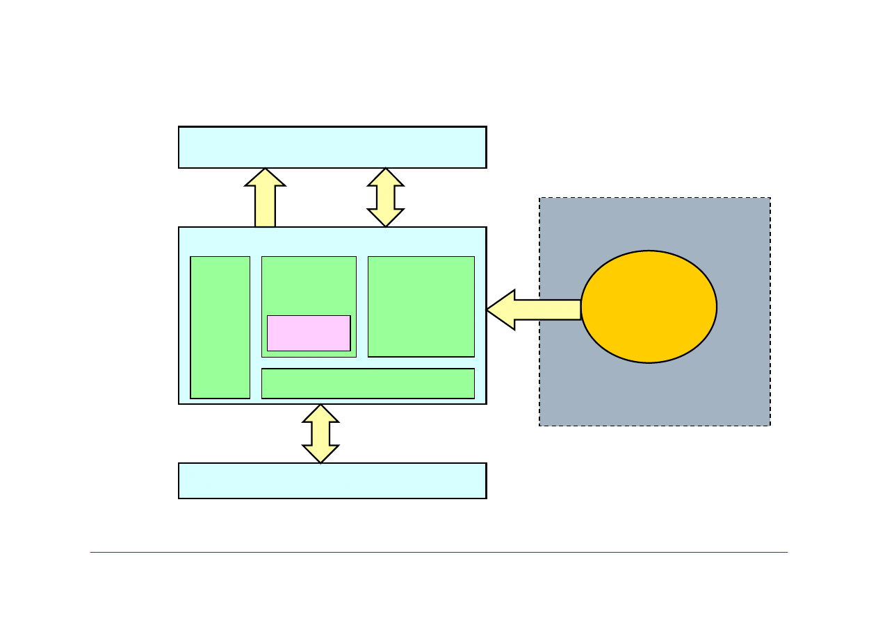
Main Memory System
Input/Output System
Arithmetic
and
Logic Unit
Operational
Registers
Program
Counter
Control Unit
Data/Instruction
Address
Central Processing Unit (CPU)
Cache
memory
Instruction
Sets

Advanced Reliable Systems (ARES) Lab.
Jin-Fu Li, EE, NCU
4
ARM Processor
¾
ARM processor was designed by Advanced RISC
Machine (ARM) Limited Company
¾
ARM processors are major used for low-power and low
cost applications
Mobile phones
Communication modems
Automotive engine management systems
Hand-held digital systems
¾
This chapter introduces the ARM instruction sets based
on the ARM7 processor
Different versions of ARM processors share the same basic
machine instruction sets

Advanced Reliable Systems (ARES) Lab.
Jin-Fu Li, EE, NCU
5
Registers and Memory Access
¾
In the ARM architecture
Memory is byte addressable
32-bit addresses
32-bit processor registers
¾
Two operand lengths are used in moving data between
the memory and the processor registers
Bytes (8 bits) and words (32 bits)
¾
Word addresses must be aligned, i.e., they must be
multiple of 4
Both little-endian and big-endian memory addressing are
supported
¾
When a byte is loaded from memory into a processor
register or stored from a register into the memory
It always located in the low-order byte position of the register
Advanced Reliable Systems (ARES) Lab.
Jin-Fu Li, EE, NCU
6
Register Structure
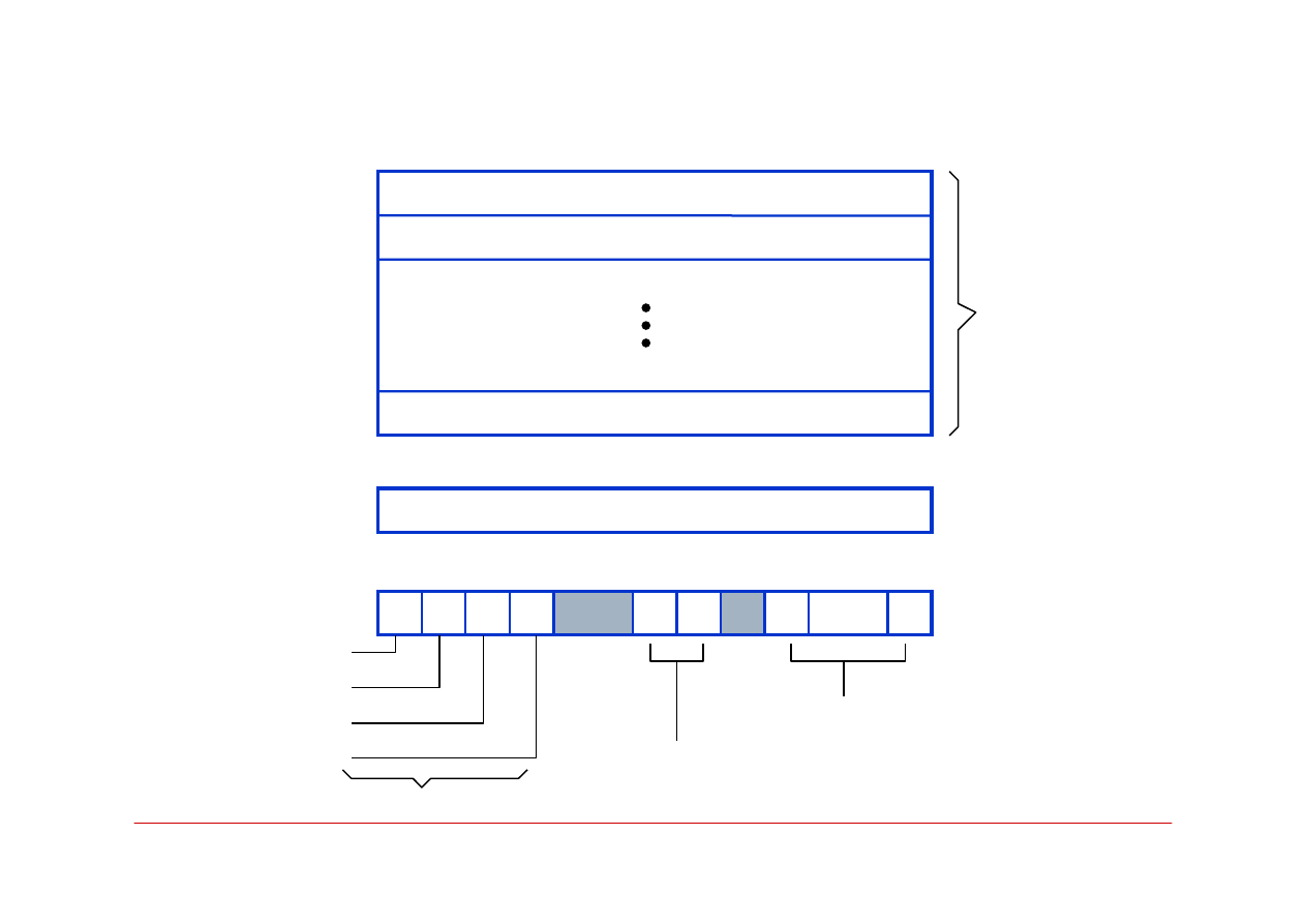
31 30 29 28
7
6
4
0
…
N-Negative
Z-Zero
C-Carry
V-Overflow
Processor mode bits
Interrupt disable bits
15
General
Purpose
registers
R0
R1
R14
31
0
31
0
R15 (PC)
Program counter
Status register
CPSR
Conditional code flags

Advanced Reliable Systems (ARES) Lab.
Jin-Fu Li, EE, NCU
7
Register Structure
¾
The use of processor mode bits and interrupt disable bits
will be described in conjunction with input/output
operations and interrupts in Chapter 5
¾
There are 15 additional general-purpose registers called
the banked registers
They are duplicates of some of the R0 to R14 registers
They are used when the processor switches into Supervisor or
Interrupt modes of operation
¾
Saved copies of the Status register are also available in the
Supervisor and Interrupt modes
¾
The banked registers and Status register copies will also
be discussed in Chapter 5

Advanced Reliable Systems (ARES) Lab.
Jin-Fu Li, EE, NCU
8
ARM Instruction Format
¾
Each instruction is encoded into a 32-bit word
¾
Access to memory is provided only by Load and Store
instructions
¾
The basic encoding format for the instructions, such as
Load, Store, Move, Arithmetic, and Logic instructions, is
shown below
¾
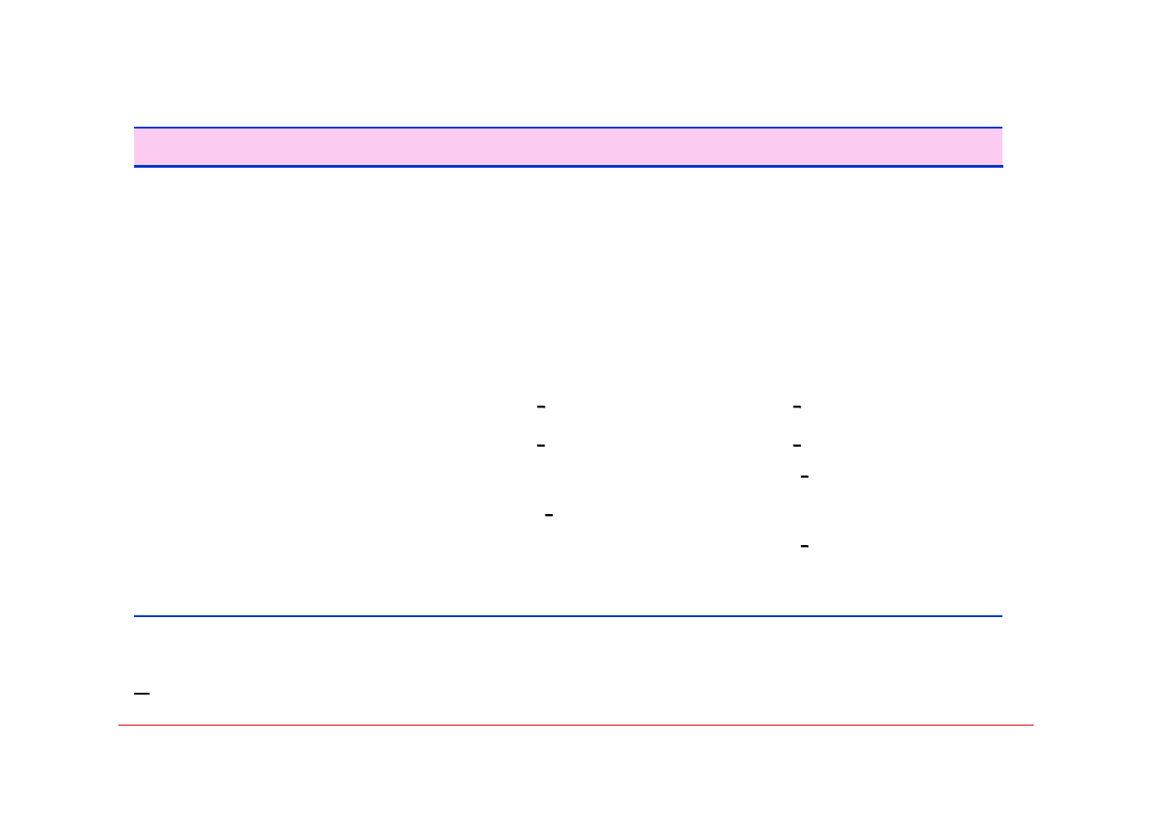
An instruction specifies a conditional execution code
(Condition), the OP code, two or three registers (Rn, Rd,
and Rm), and some other information
Condition
OP code
Rn
Rd
Rm
Other info
31
28 27
20 19 16 15 12 11
4 3
0

Advanced Reliable Systems (ARES) Lab.
Jin-Fu Li, EE, NCU
9
Conditional Execution of Instructions
¾
A distinctive and somewhat unusual feature of ARM
processors is that all instructions are conditionally
executed
Depending on a condition specified in the instruction
¾
The instruction is executed only if the current state of the
processor condition code flag satisfies the condition
specified in bits b
31
-b
28
of the instruction
Thus the instructions whose condition is not meet the processor
condition code flag are not executed
¾
One of the conditions is used to indicate that the
instruction is always executed

Advanced Reliable Systems (ARES) Lab.
Jin-Fu Li, EE, NCU
10
Memory Addressing Modes
¾
Pre-indexed mode
The effective address of the operand is the sum of the contents of
the base register Rn and an offset value
¾
Pre-indexed with writeback mode
The effective address of the operand is generated in the same way
as in the Pre-indexed mode, and then the effective address is
written back into Rn
¾
Post-indexed mode
The effective address of the operand is the contents of Rn. The
offset is then added to this address and the result is written back
into Rn
Advanced Reliable Systems (ARES) Lab.
Jin-Fu Li, EE, NCU
11
ARM Indexed Addressing Modes
With immediate offset:
Pre-indexed
Pre-indexed with writeback
Post-indexed
With offset in Rn
Pre-indexed
Pre-indexed with writeback
Post-indexed
Relative (Pre-indexed with
Immediate offset)
Name
Assembler syntax
Addressing function
[Rn, #offset]
[Rn, #offset]!
[Rn], #offest
[Rn, +Rm, shift]
[Rn, +Rm, shift]!
[Rn], +Rm, shift
Location
EA=[Rn]+offset
EA=[Rn]+offset; RnÅ[Rn]+offset
EA=[Rn]; RnÅ[Rn]+offset
EA=[Rn]+[Rm] shifted
EA=[Rn]+[Rm] shifted;
RnÅ[Rn]+[Rm] shifted
EA=[Rn];
RnÅ[Rn]+[Rm] shifted
EA=Location=[PC]+offset
shift=direction #integer, where direction is LSL for left shift or LSR for right shift, and integer
is a 5-bit unsigned number specifying the shift format
+ Rm=the offset magnitude in register Rm can be added to or subtracted from the contents
of based register Rn
Advanced Reliable Systems (ARES) Lab.
Jin-Fu Li, EE, NCU
12
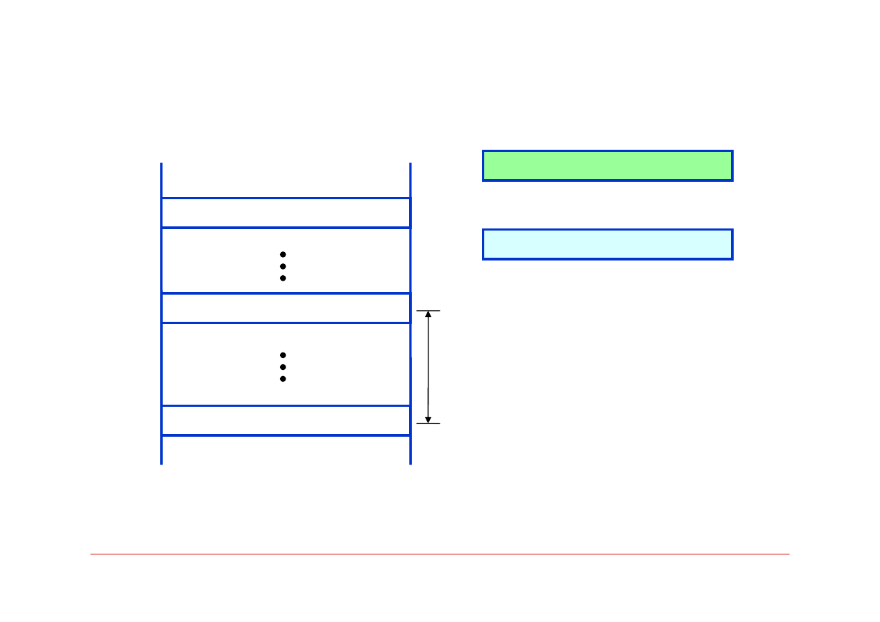
Relative Addressing Mode
LDR R1, ITEM
Operand
-
-
1000
1004
1008
ITEM=1060
Updated [PC]=1008
52=offset
Memory
address
word (4 bytes)
The operand must be within the range of 4095 bytes forward or backward from the
updated PC.
Advanced Reliable Systems (ARES) Lab.
Jin-Fu Li, EE, NCU
13
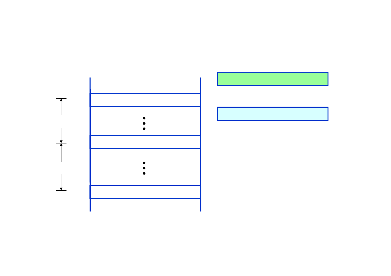
Pre-Indexed Addressing Mode
STR R3, [R5,R6]
Operand
1000
1200
1000
200=offset
R5
Based register
200
R6
Offset register
Advanced Reliable Systems (ARES) Lab.
Jin-Fu Li, EE, NCU
14
Post-Indexed Addressing with Writeback
6
321
1000
1200
1000
100=25x4
R2
Based register
25
R10
Offset register
-17
1100
100=25x4
Load instruction:
LDR R1, [R2], R10, LSL, #2

Advanced Reliable Systems (ARES) Lab.
Jin-Fu Li, EE, NCU
15
Pre-Indexed Addressing with Writeback
-
2008
2012
2012
R5
Based register (stack pointer)
27
R0
Push instruction:
STR R0, [R5,# -4]!
27
After execution of
Push instruction
TOS (top-of-stack)

Advanced Reliable Systems (ARES) Lab.
Jin-Fu Li, EE, NCU
16
Load/Store Multiple Operands
¾
In ARM processors, there are two instructions for loading
and storing multiple operands
They are called Block transfer instructions
¾
Any subset of the general purpose registers can be loaded
or stored
Only word operands are allowed, and the OP codes used are
LDM (Load Multiple) and STM (Store Multiple)
¾
The memory operands must be in successive word
locations
¾
All of the forms of pre- and post-indexing with and
without writeback are available
¾
They operate on a Base register Rn specified in the
instruction and offset is always 4
LDMIA R10!, {R0,R1,R6,R7}
IA: “Increment After” corresponding to post-indexing

Advanced Reliable Systems (ARES) Lab.
Jin-Fu Li, EE, NCU
17
Arithmetic Instructions
¾
The basic expression for arithmetic instructions is
OPcode Rd, Rn, Rm
¾
For example, ADD R0, R2, R4
Performs the operation R0Å[R2]+[R4]
¾
SUB R0, R6, R5
Performs the operation R0Å[R6]-[R5]
¾
Immediate mode: ADD R0, R3, #17
Performs the operation R0Å[R3]+17
¾
The second operand can be shifted or rotated before being
used in the operation
For example, ADD R0, R1, R5, LSL #4 operates as follows: the
second operand stored in R5 is shifted left 4-bit positions
(equivalent to [R5]x16), and its is then added to the contents of
R1; the sum is placed in R0

Advanced Reliable Systems (ARES) Lab.
Jin-Fu Li, EE, NCU
18
Logic Instructions
¾
The logic operations AND, OR, XOR, and Bit-Clear are
implemented by instructions with the OP codes AND,
ORR, EOR, and BIC.
¾
For example
AND R0, R0, R1: performs R0Å[R0]+[R1]
¾
The Bit-Clear instruction (BIC) is closely related to the
AND instruction.
It complements each bit in operand Rm before ANDing them
with the bits in register Rn.
For example, BIC R0, R0, R1. Let R0=02FA62CA, R1=0000FFFF.
Then the instruction results in the pattern 02FA0000 being placed
in R0
¾
The Move Negative instruction complements the bits of
the source operand and places the result in Rd.
For example, MVN R0, R3

Advanced Reliable Systems (ARES) Lab.
Jin-Fu Li, EE, NCU
19
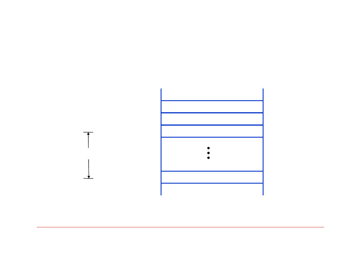
Branch Instructions
¾
Conditional branch instructions contain a signed 24-bit
offset that is added to the updated contents of the
Program Counter to generate the branch target address
¾
The format for the branch instructions is shown as below
Offset is a signed 24-bit number. It is shifted left two-bit positions
(all branch targets are aligned word addresses), signed extended
to 32 bits, and added to the updated PC to generate the branch
target address
The updated points to the instruction that is two words (8 bytes)
forward from the branch instruction
Condition
OP code
offset
31
27
28
24 23
0
Advanced Reliable Systems (ARES) Lab.
Jin-Fu Li, EE, NCU
20
ARM Branch Instructions
¾
The BEQ instruction (Branch if Equal to 0) causes a
branch if the Z flag is set to 1
1000
1004
BEQ LOCATION
Branch target instruction
Updated [PC]=1008
LOCATION=1100
Offset=92

Advanced Reliable Systems (ARES) Lab.
Jin-Fu Li, EE, NCU
21
Setting Condition Codes
¾
Some instructions, such as Compare, given by
CMP Rn, Rm which performs the operation [Rn]-[Rm] have the
sole purpose of setting the condition code flags based on the
result of the subtraction operation
¾
The arithmetic and logic instructions affect the condition
code flags only if explicitly specified to do so by a bit in
the OP-code field. This is indicated by appending the
suffix S to the OP-code
For example, the instruction ADDS R0, R1, R2 set the condition
code flags
But ADD R0, R1, R2 does not

Advanced Reliable Systems (ARES) Lab.
Jin-Fu Li, EE, NCU
22
An Example of Adding Numbers
LDR R1, N Load count into R1
LDR R2, POINTER Load address NUM1 into R2
MOV R0, #0 Clear accumulator R0
LOOP LDR R3, [R2], #4 Load next number into R3
ADD R0, R0, R3 Add number into R0
SUBS R1, R1, #1 Decrement loop counter R1
BGT LOOP Branch back if not done
STR R0, SUM Store sum
Assume that the memory location N, POINTER, and SUM are within the range
Reachable by the offset relative to the PC
GT: signed greater than
BGT: Branch if Z=0 and N=0

Advanced Reliable Systems (ARES) Lab.
Jin-Fu Li, EE, NCU
23
Assembly Language
¾
The ARM assembly language has assembler directives to
reserve storage space, assign numerical values to address
labels and constant symbols, define where program and data
blocks are to be placed in memory, and specify the end of the
source program text
¾
The AREA directive, which uses the argument CODE or
DATA, indicates the beginning of a block of memory that
contains either program instructions or data
¾
The ENTRY directive specifies that program execution is to
begin at the following LDR instruction
¾
In the data area, which follows the code area, the DCD
directives are used to label and initialize the data operands

Advanced Reliable Systems (ARES) Lab.
Jin-Fu Li, EE, NCU
24
An Example of Assembly Language
Assembler directives
AREA CODE
ENTRY
Statements that
LDR R1, N
generate
LDR R2, POINTER
machine
MOV R0, #0
instructions
LOOP LDR R3, [R2], #4
ADD R0, R0, R3
SUBS R1, R1, #1
BGT LOOP
STR R0, SUM
Assembler directives
AREA DATA
SUM DCD 0
N DCD 5
POINTER DCD NUM1
NUM1 DCD 3, -17, 27, -12, 322
END

Advanced Reliable Systems (ARES) Lab.
Jin-Fu Li, EE, NCU
25
Assembly Language
¾
An EQU directive can be used to define symbolic names
for constants
¾
For example, the statement
TEN EQU 10
¾
When a number of registers are used in a program, it is
convenient to use symbolic names for them that relate to
their usage
The RN directive is used for this purpose
For example, COUNTER RN 3 establishes the name COUNTER
for register R3
¾
The register names R0 to R15, PC (for R15), and LR( for
R14) are predefined by the assembler
R14 is used for a link register (LR)

Advanced Reliable Systems (ARES) Lab.
Jin-Fu Li, EE, NCU
26
Pseudo-Instructions
¾
An alternative way of loading the address into register R2
is also provided in the assembly language
¾
The pseudo-instruction ADR Rd, ADDRESS holds the 32-
bit value ADDRESS into Rd
This instruction is not an actual machine instruction
The assembler chooses appropriate real machine instructions to
implement pseudo-instructions
¾
For example,
The combination of the machine instruction LDR R2, POINTER
and the data declaration directive POINTER DCD NUM1 is one
way to implement the pseudo-instruction ADR R2, NUM1

Advanced Reliable Systems (ARES) Lab.
Jin-Fu Li, EE, NCU
27
Subroutines
¾
A Branch and Link (BL) instruction is used to call a
subroutine
¾
The return address is loaded into register R14, which acts
as a link register
¾
When subroutines are nested, the contents of the link
register must be saved on a stack by the subroutine.
Register R13 is normally used as the pointer for this stack

Advanced Reliable Systems (ARES) Lab.
Jin-Fu Li, EE, NCU
28
Calling program
LDR R1, N
LDR R2, POINTER
BL LISTADD
STR R0, SUM
.
.
.
Subroutine
LISTADD STMFD R13!, {R3, R14} Save R3 and return address in R14 on
stack, using R13 as the stack pointer
MOV R0, #0
LOOP LDR R3, [R2], #4
ADD R0, R0, R3
SUBS R1, R1, #1
BGT LOOP
LDMFD R13!, {R3, R15} Restore R3 and load return address into
PC (r15)
Example

Advanced Reliable Systems (ARES) Lab.
Jin-Fu Li, EE, NCU
29
Byte-Sorting Program
for (j=n-1; j>0; j=j-1)
{ for (k=j-1; k>=0; k=k-1)
{ if (LIST[k]>LIST[j])
{ TEMP=LIST[k];
LIST[k]=LIST[j];
LIST[j]=TEMP;
}
}
}
…
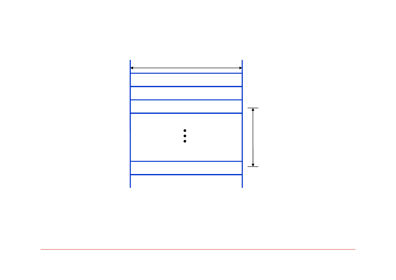
0
n-1
n-2
1
j
k

Advanced Reliable Systems (ARES) Lab.
Jin-Fu Li, EE, NCU
30
Byte-Sorting Program
ADR R4,LIST Load list pointer register R4
LDR R10,N Initialize outer loop base
ADD R2,R4,R10 Register R2 to LIST+n
ADD R5,R4, #1 Load LIST+1 into R5
OUTER LDRB R0,[R2,# -1]! Load LIST(j) into R0
MOV R3,R2 Initialize inner loop base register R3 to LIST+n-1
INNER LDRB R1,[R3, # -1]! Load LIST(k) into R1
CMP R1,R0 Compare LIST(k) to LIST(j)
If LIST(k)>LIST(j),
STRGTB R1,[R2] interchange LIST(k) and LIST(j)
STRGTB R0,[R3]
MOVGT R0,R1 Move (new) LIST(j) into R0
CMP R3,R4 If k>0, repeat
BNE INNER inner loop
CMP R2,R5 If j>1, repeat
BNE OUTER outer loop
Wyszukiwarka
Podobne podstrony:
1SBC100122C0202 Ch04 Nieznany
CH04
Genomes3e ppt ch04
ch04
ch04
ch04
CH04
Ch04 Templates
CH04
ai9 cib ch04 pentool
Essentials of Biology mad86161 ch04
Ch04 Solations Brigham 10th E
DKE285 ch04
1587200651 CH04
budynas SM ch04
więcej podobnych podstron