
JTAG Programmer Guide
Printed in U.S.A.
JTAG
Programmer
Guide
Introduction
Hardware
JTAG Programmer Tutorial
Designing Boundary Scan
and ISP Systems
Boundary Scan Basics
JTAG Parallel Download
Cable Schematic
Troubleshooting Guide
Error Messages
Using the Command Line
Interface
Standard Methodologies for
Instantiating the BSCAN

JTAG Programmer Guide
Xilinx Development System
The Xilinx logo shown above is a registered trademark of Xilinx, Inc.
FPGA Architect, FPGA Foundry, NeoCAD, NeoCAD EPIC, NeoCAD PRISM, NeoROUTE, Timing Wizard, TRACE,
XACT, XILINX, XC2064, XC3090, XC4005, XC5210, and XC-DS501 are registered trademarks of Xilinx, Inc.
The shadow X shown above is a trademark of Xilinx, Inc.
All XC-prefix product designations, A.K.A. Speed, Alliance Series, AllianceCORE, BITA, CLC, Configurable Logic
Cell, CORE Generator, CoreGenerator, CoreLINX, Dual Block, EZTag, FastCLK, FastCONNECT, FastFLASH,
FastMap, Foundation, HardWire, LCA, LogiBLOX, Logic Cell, LogiCORE, LogicProfessor, MicroVia, PLUSASM,
PowerGuide, PowerMaze, QPro, RealPCI, RealPCI 64/66, SelectI/O, Select-RAM, Select-RAM+, Smartguide,
Smart-IP, SmartSearch, Smartspec, SMARTSwitch, Spartan, TrueMap, UIM, VectorMaze, VersaBlock,
VersaRing, Virtex, WebLINX, XABEL, XACT
step, XACTstep Advanced, XACTstep Foundry, XACT-Floorplanner,
XACT-Performance, XAM, XAPP, X-BLOX, X-BLOX plus, XChecker, XDM, XDS, XEPLD, Xilinx Foundation
Series, XPP, XSI, and ZERO+ are trademarks of Xilinx, Inc. The Programmable Logic Company and The
Programmable Gate Array Company are service marks of Xilinx, Inc.
All other trademarks are the property of their respective owners.
Xilinx, Inc. does not assume any liability arising out of the application or use of any product described or shown
herein; nor does it convey any license under its patents, copyrights, or maskwork rights or any rights of others.
Xilinx, Inc. reserves the right to make changes, at any time, in order to improve reliability, function or design and
to supply the best product possible. Xilinx, Inc. will not assume responsibility for the use of any circuitry described
herein other than circuitry entirely embodied in its products. Xilinx, Inc. devices and products are protected under
one or more of the following U.S. Patents: 4,642,487; 4,695,740; 4,706,216; 4,713,557; 4,746,822; 4,750,155;
4,758,985; 4,820,937; 4,821,233; 4,835,418; 4,855,619; 4,855,669; 4,902,910; 4,940,909; 4,967,107; 5,012,135;
5,023,606; 5,028,821; 5,047,710; 5,068,603; 5,140,193; 5,148,390; 5,155,432; 5,166,858; 5,224,056; 5,243,238;
5,245,277; 5,267,187; 5,291,079; 5,295,090; 5,302,866; 5,319,252; 5,319,254; 5,321,704; 5,329,174; 5,329,181;
5,331,220; 5,331,226; 5,332,929; 5,337,255; 5,343,406; 5,349,248; 5,349,249; 5,349,250; 5,349,691; 5,357,153;
5,360,747; 5,361,229; 5,362,999; 5,365,125; 5,367,207; 5,386,154; 5,394,104; 5,399,924; 5,399,925; 5,410,189;
5,410,194; 5,414,377; 5,422,833; 5,426,378; 5,426,379; 5,430,687; 5,432,719; 5,448,181; 5,448,493; 5,450,021;
5,450,022; 5,453,706; 5,455,525; 5,466,117; 5,469,003; 5,475,253; 5,477,414; 5,481,206; 5,483,478; 5,486,707;
5,486,776; 5,488,316; 5,489,858; 5,489,866; 5,491,353; 5,495,196; 5,498,979; 5,498,989; 5,499,192; 5,500,608;
5,500,609; 5,502,000; 5,502,440; 5,504,439; 5,506,518; 5,506,523; 5,506,878; 5,513,124; 5,517,135; 5,521,835;
5,521,837; 5,523,963; 5,523,971; 5,524,097; 5,526,322; 5,528,169; 5,528,176; 5,530,378; 5,530,384; 5,546,018;
5,550,839; 5,550,843; 5,552,722; 5,553,001; 5,559,751; 5,561,367; 5,561,629; 5,561,631; 5,563,527; 5,563,528;
5,563,529; 5,563,827; 5,565,792; 5,566,123; 5,570,051; 5,574,634; 5,574,655; 5,578,946; 5,581,198; 5,581,199;
5,581,738; 5,583,450; 5,583,452; 5,592,105; 5,594,367; 5,598,424; 5,600,263; 5,600,264; 5,600,271; 5,600,597;
5,608,342; 5,610,536; 5,610,790; 5,610,829; 5,612,633; 5,617,021; 5,617,041; 5,617,327; 5,617,573; 5,623,387;
5,627,480; 5,629,637; 5,629,886; 5,631,577; 5,631,583; 5,635,851; 5,636,368; 5,640,106; 5,642,058; 5,646,545;
5,646,547; 5,646,564; 5,646,903; 5,648,732; 5,648,913; 5,650,672; 5,650,946; 5,652,904; 5,654,631; 5,656,950;
5,657,290; 5,659,484; 5,661,660; 5,661,685; 5,670,896; 5,670,897; 5,672,966; 5,673,198; 5,675,262; 5,675,270;
5,675,589; 5,677,638; 5,682,107; 5,689,133; 5,689,516; 5,691,907; 5,691,912; 5,694,047; 5,694,056; 5,724,276;
5,694,399; 5,696,454; 5,701,091; 5,701,441; 5,703,759; 5,705,932; 5,705,938; 5,708,597; 5,712,579; 5,715,197;
5,717,340; 5,719,506; 5,719,507; 5,724,276; 5,726,484; 5,726,584; 5,734,866; 5,734,868; 5,737,234; 5,737,235;
5,737,631; 5,742,178; 5,742,531; 5,744,974; 5,744,979; 5,744,995; 5,748,942; 5,748,979; 5,752,006; 5,752,035;
5,754,459; 5,758,192; 5,760,603; 5,760,604; 5,760,607; 5,761,483; 5,764,076; 5,764,534; 5,764,564; 5,768,179;
5,770,951; 5,773,993; 5,778,439; 5,781,756; 5,784,313; 5,784,577; 5,786,240; 5,787,007; 5,789,938; 5,790,479;
R

JTAG Programmer Guide
5,790,882; 5,795,068; 5,796,269; 5,798,656; 5,801,546; 5,801,547; 5,801,548; 5,811,985; 5,815,004; 5,815,016;
5,815,404; 5,815,405; 5,818,255; 5,818,730; 5,821,772; 5,821,774; 5,825,202; 5,825,662; 5,825,787; 5,828,230;
5,828,231; 5,828,236; 5,828,608; 5,831,448; 5,831,460; 5,831,845; 5,831,907; 5,835,402; 5,838,167; 5,838,901;
5,838,954; 5,841,296; 5,841,867; 5,844,422; 5,844,424; 5,844,829; 5,844,844; 5,847,577; 5,847,579; 5,847,580;
5,847,993; 5,852,323; Re. 34,363, Re. 34,444, and Re. 34,808. Other U.S. and foreign patents pending. Xilinx,
Inc. does not represent that devices shown or products described herein are free from patent infringement or from
any other third party right. Xilinx, Inc. assumes no obligation to correct any errors contained herein or to advise
any user of this text of any correction if such be made. Xilinx, Inc. will not assume any liability for the accuracy or
correctness of any engineering or software support or assistance provided to a user.
Xilinx products are not intended for use in life support appliances, devices, or systems. Use of a Xilinx product in
such applications without the written consent of the appropriate Xilinx officer is prohibited.
Copyright 1991-1999 Xilinx, Inc. All Rights Reserved.

JTAG Programmer Guide
i
About This Manual
This manual describes Xilinx’s JTAG Programmer software, a tool
used for In-system progamming.
Before using this manual, you should be familiar with the operations
that are common to all Xilinx’s software tools: how to bring up the
system, select a tool for use, specify operations, and manage design
data. These topics are covered in the Development System Reference
Guide.
Additional Resources
For additional information, go to http://support.xilinx.com. The
following table lists some of the resources you can access from this
page. You can also directly access some of these resources using the
provided URLs.
Resource
Description/URL
Tutorial
Tutorials covering Xilinx design flows, from design entry to verification
and debugging
http://support.xilinx.com/support/techsup/tutorials/index.htm
Answers
Database
Current listing of solution records for the Xilinx software tools
Search this database using the search function at
http://support.xilinx.com/support/searchtd.htm
Application
Notes
Descriptions of device-specific design techniques and approaches
http://support.xilinx.com/apps/appsweb.htm
Data Book
Pages from The Programmable Logic Data Book, which describe device-
specific information on Xilinx device characteristics, including read-
back, boundary scan, configuration, length count, and debugging
http://support.xilinx.com/partinfo/databook.htm

Preface
ii
Xilinx Development System
Manual Contents
This manual covers the following topics.
•
“Introduction” chapter describes JTAG Programmer software.
•
“Hardware” chapter provides information for connecting and
using the XChecker Serial Cable or the Parallel Download Cable
for system operation.
•
“JTAG Programmer Tutorial” chapter documents the basic tasks
needed to download programming to XC9500/XL/XV family
devices in-system.
•
“Designing Systems with FPGA's Enabled for Boundary-Scan
Operations” chapter documents using the JTAG Programmer
with FPGA devices.
•
“Boundary Scan Basics” appendix contains reference information
about boundary scan basics.
•
“JTAG Parallel Download Cable Schematic” appendix has sche-
matics for the XChecker Cable and the Parallel Download Cable.
•
“Troubleshooting Guide” appendix contains troubleshooting
information.
•
“Error Messages” appendix provides a list of error messages that
the JTAG Programmer may report. For most error messages a
workaround is suggested.
•
“Using the Command Line Interface” appendix documents the
basics of using the JTAG Programmer from a command line in a
workstation environment.
•
“Standard Methodologies for Instantiating the BSCAN Symbol”
appendix contains programming examples.
Xcell Journals
Quarterly journals for Xilinx programmable logic users
http://support.xilinx.com/xcell/xcell.htm
Tech Tips
Latest news, design tips, and patch information on the Xilinx design
environment
http://support.xilinx.com/support/techsup/journals/index.htm
Resource
Description/URL

JTAG Programmer Guide
v
Conventions
This manual uses the following typographical and online document
conventions. An example illustrates each typographical convention.
Typographical
The following conventions are used for all documents.
•
Courier font
indicates messages, prompts, and program files
that the system displays.
speed grade: -100
•
Courier bold
indicates literal commands that you enter in a
syntactical statement. However, braces “{ }” in Courier bold are
not literal and square brackets “[ ]” in Courier bold are literal
only in the case of bus specifications, such as bus [7:0].
rpt_del_net=
Courier bold
also indicates commands that you select from a
menu.
File
→
Open
•
Italic font denotes the following items.
•
Variables in a syntax statement for which you must supply
values
edif2ngd
design_name
•
References to other manuals
See the Development System Reference Guide for more informa-
tion.

JTAG Programmer Guide
vi
Xilinx Development System
•
Emphasis in text
If a wire is drawn so that it overlaps the pin of a symbol, the
two nets are not connected.
•
Square brackets “[ ]” indicate an optional entry or parameter.
However, in bus specifications, such as bus [7:0], they are
required.
edif2ngd
[option_name] design_name
•
Braces “{ }” enclose a list of items from which you must choose
one or more.
lowpwr =
{
on
|
off
}
•
A vertical bar “|” separates items in a list of choices.
lowpwr =
{
on
|
off
}
•
A vertical ellipsis indicates repetitive material that has been
omitted.
IOB #1: Name = QOUT’
IOB #2: Name = CLKIN’
.
.
.
•
A horizontal ellipsis “. . .” indicates that an item can be repeated
one or more times.
allow block
block_name loc1 loc2
...
locn;
Online Document
The following conventions are used for online documents.
•
Red-underlined text indicates an interbook link, which is a cross-
reference to another book. Click the red-underlined text to open
the specified cross-reference.
•
Blue-underlined text indicates an intrabook link, which is a cross-
reference within a book. Click the blue-underlined text to open
the specified cross-reference.

JTAG Programmer Guide
1-1
Chapter 1
Introduction
This chapter introduces you to the basic concepts of Xilinx JTAG
capabilities and Xilinx in-system programmable products. You can
use JTAG Programmer to download, read back and verify design
configuration data, to perform functional tests on any device, and to
probe internal logic states of a Xilinx XC9500, XC9500XL, XC9500XV,
Spartan or Virtex design. This chapter contains the following
sections:
•
“Programming and Verification Overview“
•
“Required Files“
Programming and Verification Overview
JTAG Programmer software uses sequences of JTAG instructions to
perform the following programming and verification operations. The
user need only select the desired operation; the software will execute
all required JTAG commands transparently. For a description of JTAG
instructions supported by Xilinx devices, see Appendix A.
Device operation options available to users are:
Program
. Downloads the contents of the JEDEC or BIT file to the
device programming registers.
Verify
. Reads back the contents of the device programming registers
and compares them with the JEDEC or BIT file.
Erase
. Clears device configuration information.
Functional Test
. Applies user-specified functional vectors from the
JEDEC file to the device using the JTAG INTEST instruction,
comparing results obtained against expected values. Reports any
differences to the user.

Introduction
1-2
Xilinx Development System
Blank Check
. Checks whether a device has been programmed or is
erased.
Readback Jedec
. Reads back the contents of device programming
registers and creates a new JEDEC file with the results.
Get Device ID
. Reads the contents of the JTAG IDCODE register.
Displays contents for the user.
Get Device Checksum
. Reads back the contents of device program-
ming registers and calculates a checksum for comparison against the
expected value.
Get Device Signature/Usercode.
This value is selected by the user
during fitting. The specified value is translated to binary values in the
JEDEC file. During device programming these values are loaded into
the JTAG USERCODE register. This function reads the contents of the
USERCODE register and displays the result.
Bypass
. Ignores this device when addressing devices in the JTAG
boundary scan chain. This option is only available through chain
operations.
Non-Volatile Device Data Security
Any Xilinx XC9500/XL/XV device selected for programming can be
secured with the
Write Protect
or
Read Protect
or both.
When enabled,
Read Protect
disables reading the programmed
contents of a device (the IDCODE and USERCODE registers remain
readable).
Write Protect
allows only the reading of the programmed data.
The device contents cannot be altered or re-programmed.
When both
Read Protect
and
Write Protect
are enabled, the
device can be neither read nor re-programmed.
Note:
Security options do not affect the accessibility of the bypass or
boundary-scan register.
User Feedback
When using the graphical user interface, immediate feedback is
provided by a scrolling log file and alert boxes. Detailed information
regarding failure is located in the system log file, and is provided for
both the PC and workstation based tool.

Introduction
JTAG Programmer Guide
1-3
Required Files
You need to provide JEDEC files for each XC9500/XL/XV CPLD
device, BIT files for each Xilinx FPGA device (Virtex or Spartan) in
the JTAG programming chain, and BSDL files for the remaining
devices.
JEDEC Files
JEDEC files are XC9500/XL/XV CPLD programming files generated
by the Xilinx fitter. They are ASCII text files containing programming
information and, optionally, functional test vectors that can be used
to verify the correct functional behavior of the programmed device.
One JEDEC file is required for each XC9500/XL/XV device in the
JTAG programming chain.
Use the device properties (
File
→
Properties
) dialog to specify
the location of JEDEC files for each XC9500/XL/XV device. The
name of the JEDEC file is assumed to be
<design name>.jed
, but
can be specified exactly by the user.
BSDL Summary
The Boundary-Scan Description Language (BSDL) files use a subset
of VHDL to describe the boundary scan features of a device. The
JTAG Programmer automatically extracts the length of the instruc-
tion register from the BSDL file to place non-XC9500/XL/XV devices
in bypass mode. One user-provided BSDL file is required for each
type of non-XC9500/XL/XV device in the JTAG programming chain.
XC9500/XL/XV BSDL files are located automatically by the JTAG
Programmer.
Use the device properties dialog to specify the location of BSDL files
for non-XC9500/XL/XV devices. The name of the BSDL file is
assumed to be
<device name>.bsd
.
BIT Files
Bit files are Xilinx FPGA configuration files generated by the Xilinx
FPGA design software. They are proprietary format binary files
containing configuration information. One BIT file is required for
each Xilinx FPGA in the JTAG boundary-scan chain.

Introduction
1-4
Xilinx Development System
Use the device properties (
File
→
Properties
) dialog to specify
the location of the BIT files for each Xilinx FPGA device. The required
extension for BIT files is
.bit
.

JTAG Programmer Guide
2-1
Chapter 2
Hardware
This chapter gives specific information about using cables to down-
load from the JTAG Programmer to devices in-system.
This chapter contains the following sections:
•
•
“XChecker Hardware (Serial)” section
•
•
“Flying Lead Connectors” section
•
Download Cables
There are two cables available for use with the JTAG Programmer.
The first is an RS232 serial cable known as the XChecker Cable. The
second is the Parallel Download Cable which can be connected to a
PC’s parallel printer port.
There are a few advantages to be considered in selecting a cable:
•
The XChecker Cable connects to the serial port of both worksta-
tions and PCs.
•
The Parallel Cable has better drive capability. The Parallel Cable
can drive up to 10 XC9500/XL/XV devices in a boundary-scan
chain, and the XChecker Cable can drive up to 4 XC9500/XL/XV
devices.
•
The Parallel Cable is at least 5 times faster.
Note:
If you have a Parallel Download Cable proceed to Parallel
Cable.

JTAG Programmer Guide
2-2
Xilinx Development System
XChecker Hardware (Serial)
The XChecker hardware consists of a cable assembly with internal
logic, a test fixture, and a set of headers to connect the cable to your
target system.
Using the XChecker hardware requires either a standard DB-9 or DB-
25 RS-232 serial port. If you have a different serial port connection,
you need to provide the appropriate adapter. “XChecker Hardware
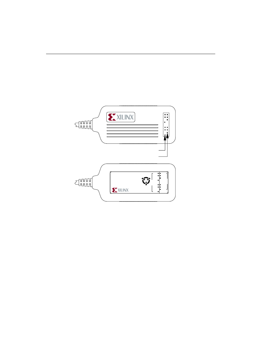
and Accessories” figure shows the XChecker cable hardware and
accessories.
The XChecker cable can be used with a single CPLD or several
devices connected in a boundary-scan chain to download and read-
back configuration and boundary-scan data.
Hardware
JTAG Programmer Guide
2-3
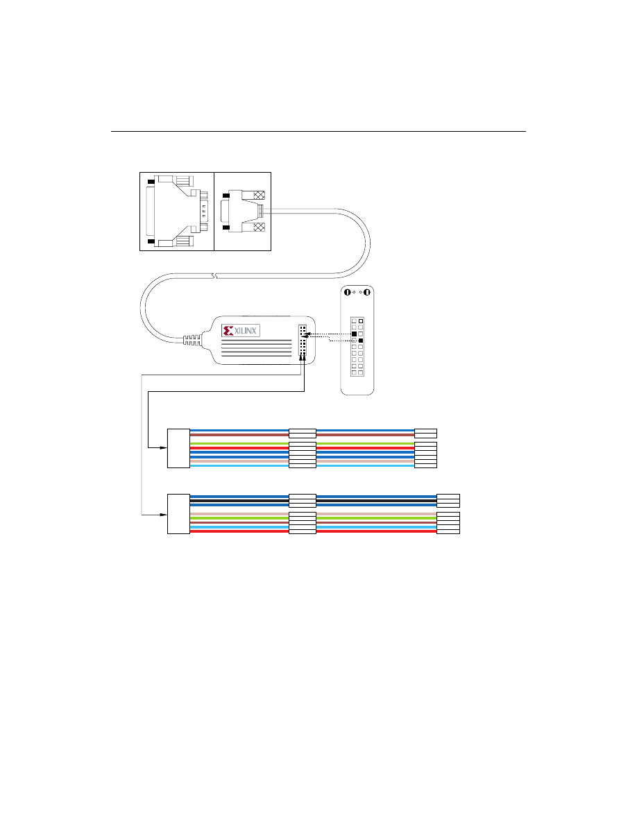
Figure 2-1
XChecker Hardware and Accessories
“XChecker Cable” figure shows top and bottom views of the
XChecker cable.
VCC
VCC
GND
CCLK
D/P
DIN
PROG
INIT
RST
TRIG
RD
RT
TDI
TCK
TMS
CLK1
CLK0
Connection to Host Computer
XChecker Cable
Flying Lead Connector 1
Header 1
Header 2
Flying Lead Connector 2
DB25 Adapter
DB9 Socket Connector
+5V
Test Fixture
(Enlarged to
show plugs)
Connections to
Target System
Connections to
Target System
GND
X7248
JTAG Programmer Guide
2-4
Xilinx Development System
Figure 2-2
XChecker Cable
Connecting for System Operation
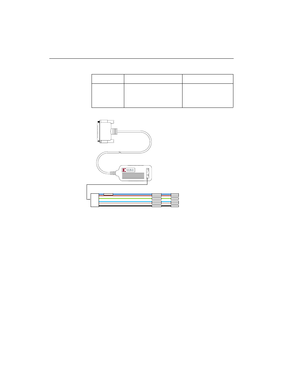
Connect the XChecker cable to the host system and your target
system as shown in “XChecker Connections to JTAG Boundary-scan
TAP” figure.
XChecker Cable
Top View
Bottom View
Header 2
Header 1
Model : DLC4
CAUTION
SENSITIVE
ELECTRONIC
DEVICE
Power : 5V 100mA Typ.
Serial: DL - 1 2 3 4 5
RT
RD
TRIG
TDI
TCK
TMS
CLKI
CLKO
VCC
Made in U.S.A
GND
CCLK
D/P
DIN
PROG
INIT
RST
X7249
Hardware
JTAG Programmer Guide
2-5
Figure 2-3
XChecker Connections to JTAG Boundary-scan TAP
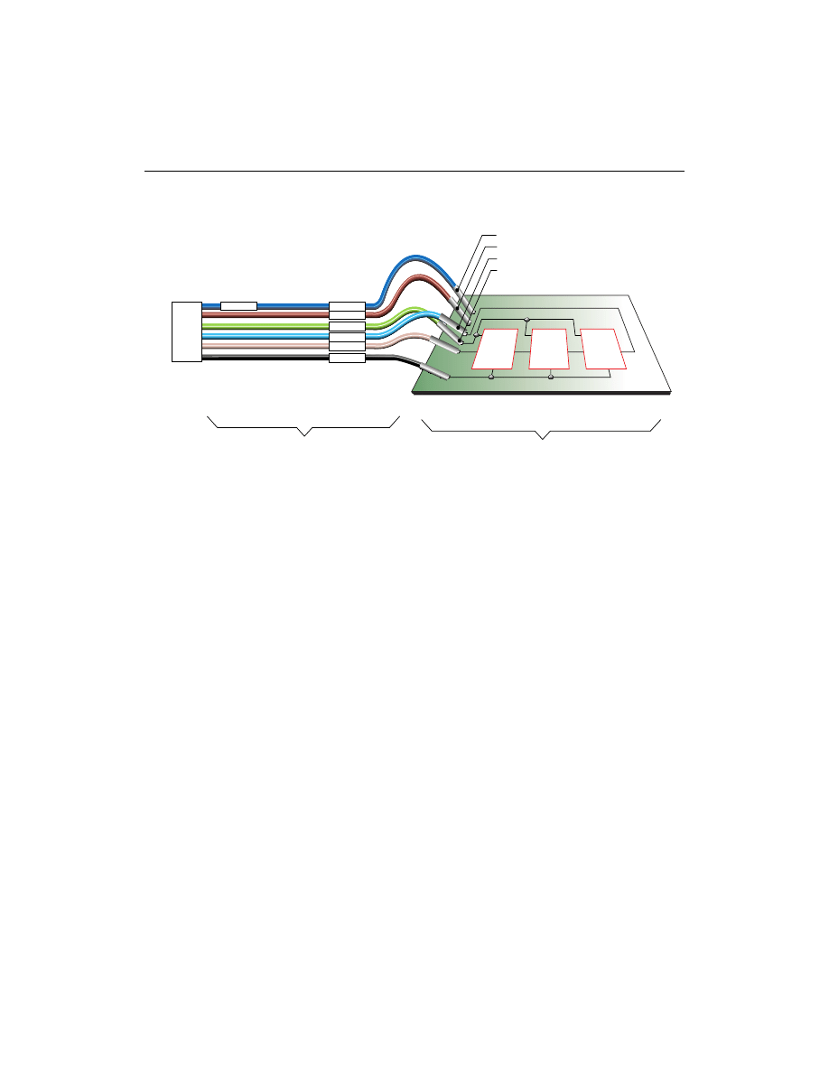
Cable Connections
Connections between the cable assembly and the target system use
only 6 of the sixteen leads. For connection to JTAG boundary-scan
systems you need only ensure that the VCC, GND, TDI, TCK, TMS
and RD (TDO) pins are connected.
Once installed properly, the connectors provide power to the cable,
allow download and readback of configuration data, and provide for
logic probe of device pins.
“XChecker Cable Connections and Definitions” table describes the
pin connections to the target circuit board.
Table 2-1
XChecker Cable Connections and Definitions
Name
Function
Connections
VCC
Power – Supplies V
CC
(5 V,
100 mA, typically) to the
cable.
To target system V
CC
GND
Ground – Supplies ground
reference to the cable.
To target system
ground
XCHECKER Flying Lead Connector
Target System
X7976
TMS
TDI TDO
TCK
TMS
TDI TDO
TCK
TMS
TDI TDO
TCK
VCC
GND
TMS
TDI
RD
TMS
TDI
TCK
RD (TDO)
TCK
GND
VCC

JTAG Programmer Guide
2-6
Xilinx Development System
RD (TDO)
Read Data – Read back
data from the target
system is read at this pin.
Connect to system
TDO pin.
TDI
Test Data In – this signal is
used to transmit serial test
instructions and data.
Connect to system TDI
pin.
TCK
Test Clock – this clock
drives the test logic for all
devices on boundary-scan
chain.
Connect to system TCK
pin.
TMS
Test Mode Select – this
signal is decoded by the
TAP controller to control
test operations.
Connect to system TMS
pin.
CLKI
Not used.
Unconnected.
CLKO
Not used.
Unconnected.
CCLK
Not used.
Unconnected.
D/P
Not used.
Unconnected.
DIN
Not used.
Unconnected.
PROG
Not used.
Unconnected.
INIT
Not used.
Unconnected.
RST
Not used.
Unconnected.
RT
Not used.
Unconnected.
TRIG
Not used.
Unconnected.
Table 2-1
XChecker Cable Connections and Definitions
Name
Function
Connections

Hardware
JTAG Programmer Guide
2-7
Baud Rates
The XChecker Cable supports Baud rates as shown in Table 2-2.
Connecting the XChecker Cable
There are two simple steps for connecting the cable:
1.
Connect the cable to your host system serial port.
2.
Connect the cable to your target system.
Connecting the XChecker Cable
The XChecker cable connects to your system RS-232 serial port. You
may need a DB-9/DB-25 adapter, which accommodates most serial
ports, so that you can connect the XChecker cable to your host
system.
The JTAG Programmer software will automatically identify the
XChecker cable when correctly connected to your computer. If you
choose to, you may also select this connection manually. To set up a
serial port manually:
Output
→
Cable Setup
Select
XChecker
, then click on
OK
. If you are using the XChecker
Cable you may also select a BAUD rate. See Table 2-1, Valid Baud
Rates.
Connection to Your Target System
You need appropriate pins on the target system for connecting the
target system board to the header connection on the cable. These
connectors must be standard 0.025
−
inch square male pins that have
dedicated traces to the target system control pins. You connect to
these pins with the flying lead connectors.
Table 2-2
Valid Baud Rates
Platform
9600 19200
38400
IBM PC
X
X
X
SUN
X
X
X
HP 700
X
X
X

JTAG Programmer Guide
2-8
Xilinx Development System
Note:
The XChecker cable draws its power from the target system
through V
CC
and GND. Therefore, power to XChecker, as well as to
the target system, must be stable. Do not connect any signals before
connecting V
CC
and ground.
Note:
If your system‘s power is turned off before or during JTAG
Programmer operations, the cable will not operate. Your system’s
power should be on during JTAG Programming operations.
Note:
If the power has been momentarily interrupted, go to
Output
→
Cable Reset
to reinitialize the XChecker cable. If you do not
want to operate at maximum Baud rate, go to the
Cable
Communi-
cation
Setup
dialog box (
Output
→
Cable Setup...
) and set a
lower rate.
Parallel Cable
The Parallel Download Cable consists of a cable assembly containing
logic to protect your PC‘s parallel port and a set of headers to connect
to your target system.
Using the Parallel Download Cable requires a PC equipped with an
AT compatible parallel port interface with a DB25 standard printer
connector. Figure 2-4 shows the Parallel Download Cable.
Hardware
JTAG Programmer Guide
2-9
Figure 2-4
Parallel Download Cable and Accessories
The cable assembly contains logic designed to electrically isolate the
target system from the parallel port of your PC host system.
The parallel download cable can be used with a single CPLD or
several connected in a boundary-scan chain to download and read-
back configuration and boundary-scan data.
The transmission speed of the Parallel Download Cable is deter-
mined solely by the speed at which the host PC can transmit data
through its parallel port interface.
Figure 2-5 shows top and bottom view of the Parallel Download
Cable.
JTAG
VCC
GND
TCK
TDO
TDI
TMS
JTAG Flying Lead Connector
Connections to
Target System
DB25 Plug Connector
Parallel Cable
X7251
JTAG Programmer Guide
2-10
Xilinx Development System
Figure 2-5
Top and Bottom View of Parallel Download Cable
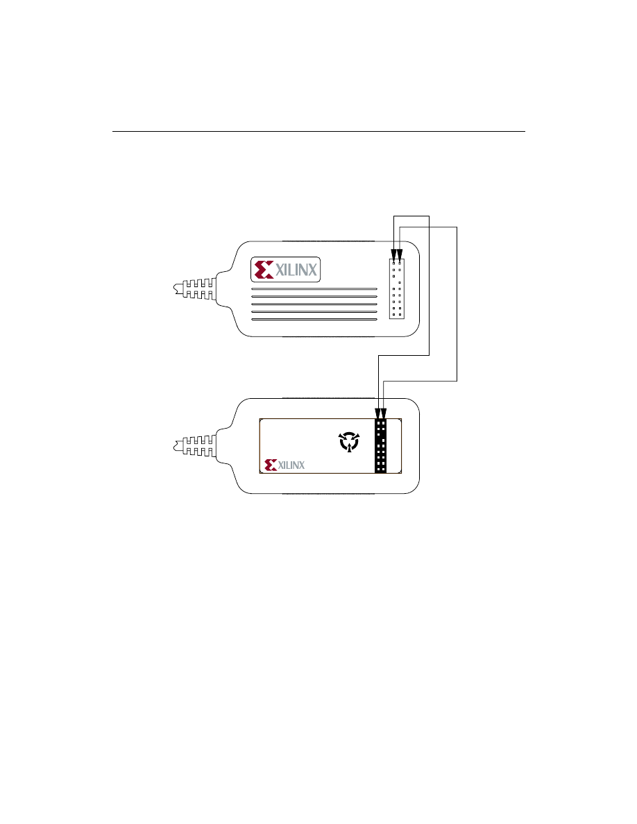
Connecting for System Operation
Connect the parallel cable to the host system and your target system
as shown in Figure 2-6.
Parallel Cable
Top View
Bottom View
JTAG Header
FPGA Header
Parallel Cable III
CAUTION
SENSITIVE
ELECTRONIC
DEVICE
Model DLC5
Power 5V 10mA Typ.
Serial JT - 1 2 3 4 5
VCC
JTAG
FPGA
GND
TCK
TDO
TDI
TMS
VCC
Made in U.S.A
GND
CCLK
D/P
DIN
PROG
X7252
Hardware
JTAG Programmer Guide
2-11
Figure 2-6
Parallel Download Cable Connection to JTAG
Boundary-scan TAP
Appendix B contains schematic diagrams of the Parallel Download
Cable.
Configuring the Parallel Download Cable
On PCs you can connect the parallel cable to your system’s parallel
printer port. The JTAG Programmer software will automatically iden-
tify the cable when correctly connected to your PC. If you choose to,
you may also select this connection manually. To set up a parallel port
manually:
Output
→
Cable Setup
Select the
Parallel
box and match to the port you are using, then
click on
OK
.
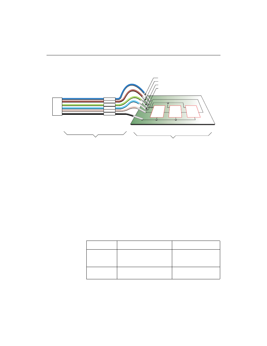
Flying Lead Connectors
The flying lead connector has a 9-pin (6 signals, 3 keys) header
connector that fits onto the cable’s JTAG header. The pin order is
listed in Table 2-3. These header connectors are keyed to assure
JTAG Flying Lead Connector
Target System
X8005
TMS
TDI TDO
TCK
TMS
TDI TDO
TCK
TMS
TDI TDO
TCK
VCC
GND
TMS
TCK
JTAG
TMS
TDI
TDO
TDI
TCK
TDO
GND
VCC

JTAG Programmer Guide
2-12
Xilinx Development System
proper orientation to the cable assembly.
The flying lead connector has six individual female connectors on one
end that fit onto standard 0.025
″
square male pins. Each lead is
labeled to identify the proper pin connection.
When you layout the printed circuit board for use with JTAG in-
system programming and testing, a few adjustments will make the
process of connecting and downloading easier.
•
Provide pins on your printed circuit board for VCC, GND, TCK,
TDO, TDI and TMS.
•
These pins must be standard 0.025” square male pins that have
dedicated traces to the target system control pins. You connect to
these pins with the flying lead connector.
•
Place pins on board so that flying leads can reach them. The
length of our flying leads is six inches. While pins may be a
couple inches apart, do not have any two JTAG pins more than
six inches apart.
•
Keep header pins on your board a minimum of 0.10” apart.
Table 2-3
Parallel Cable Connections and Definitions
Name
Function
Connections
VCC
Power – Supplies V
CC
(5 V,
10 mA, typically) to the
cable.
To target system V
CC
GND
Ground – Supplies ground
reference to the cable.
To target system
ground
TCK
Test Clock – this clock
drives the test logic for all
devices on boundary-scan
chain.
Connect to system TCK
pin.
TDO
Read Data – Read back
data from the target
system is read at this pin.
Connect to system
TDO pin.
TDI
Test Data In – this signal is
used to transmit serial test
instructions and data.
Connect to system TDI
pin.
Hardware
JTAG Programmer Guide
2-13
Figure 2-7
JTAG Cable and Leads (parallel cable shown)
Power Up Sequencing
1.
Connect your cable to your host computer.
2.
Turn the power to your target system off, if possible.
3.
The power for the drivers is derived from the target system.
Connect the cable’s GND wire to the corresponding signal on the
target board. Next, connect VCC to the corresponding signal on
the target board.
Note:
Download cables will not operate if the target system‘s power
is turned off before or during JTAG Programmer operations. Make
TMS
Test Mode Select – this
signal is decoded by the
TAP controller to control
test operations.
Connect to system TMS
pin.
Table 2-3
Parallel Cable Connections and Definitions
Name
Function
Connections
JTAG
VCC
GND
TCK
TDO
TDI
TMS
JTAG Flying Lead Connector
Connections to
Target System
DB25 Plug Connector
Parallel Cable
X7251

JTAG Programmer Guide
2-14
Xilinx Development System
certain that this power connection is on and stable. Your system’s
power should be on during JTAG Programmer operations.
Note:
JTAG Programmer will always initiate operations using a JTAG
TAP controlled reset sequence. This performs the exact same opera-
tion as the assertion of the TRST pin; it initializes all devices‘ JTAG
state machines and internal registers.
4.
Next connect the JTAG TAP inputs. Connect TCK, TDI, TMS and
TDO to the target board. TRST is not supported by the XC9500/
XL/XV JTAG Download Cables. If any of your JTAG parts have a
TRST pin, it should be connected to VCC.
5.
Power up the target system.
Warning:
Cable protection ensures that the parallel port cannot be
damaged through normal cable operation. For increased safety,
please check that the power to the system controller is on before the
target system is powered up.

JTAG Programmer Guide
3-1
Chapter 3
JTAG Programmer Tutorial
This chapter will take you through the basic steps involved in
programming Xilinx devices in-system using the JTAG Programmer
graphical user interface. This chapter contains the following sections:
•
“Cable Setup” section
•
“Selecting a Port for the Cable” section
•
“Creating New Chain Descriptions” section
•
“Configuring a Device In-System” section
•
“Generating SVF Files” section
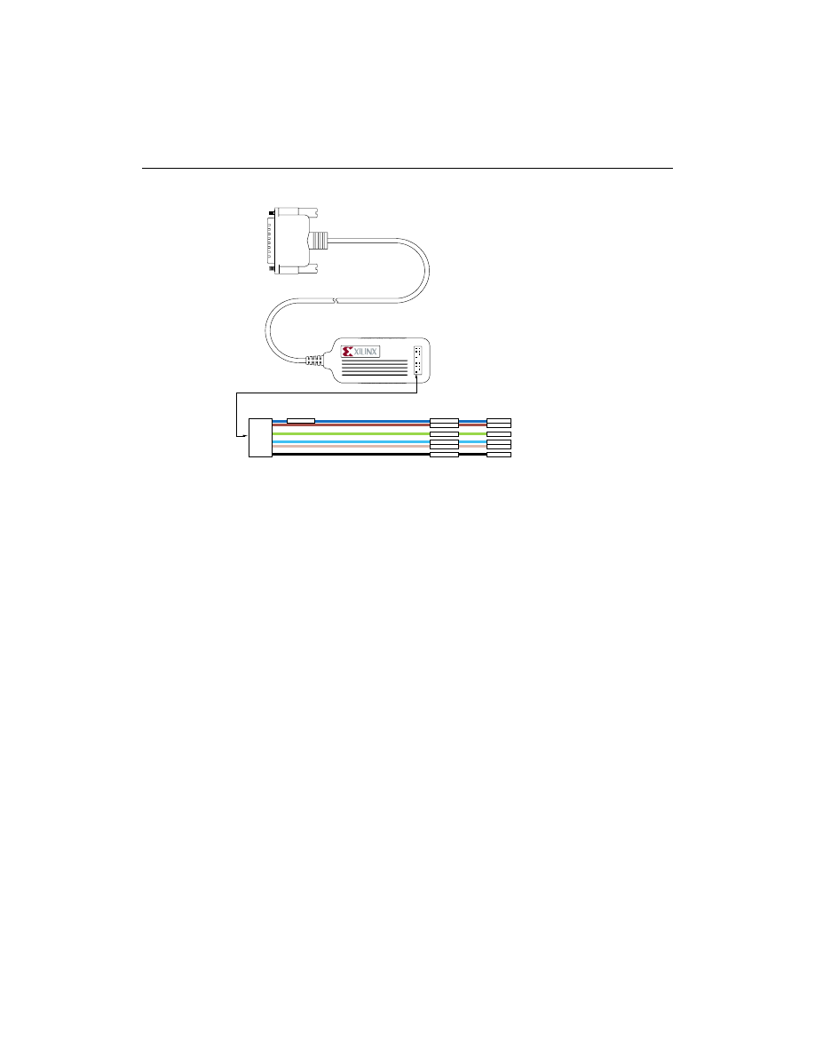
Cable Setup
To setup your system to download configurations in-system you
must first connect the JTAG Programmer parallel download cable or
the XChecker cable. Cable setups and power sequencing are
described in chapter 2, Hardware.
Selecting a Port for the Cable
You may select a serial or parallel port for your cable from the JTAG
Programmer Interface. To set up a port:
Output
→
Cable Setup
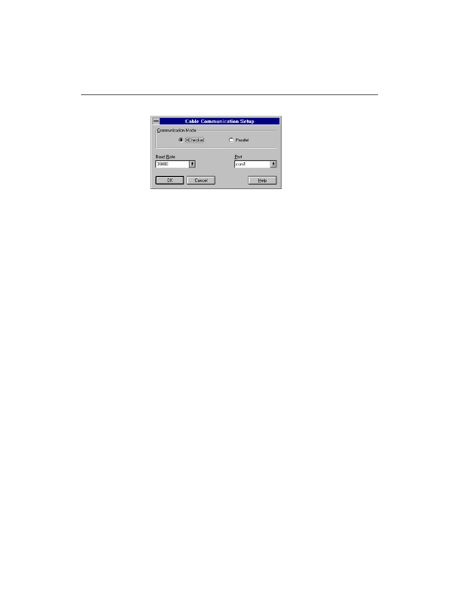
The
Cable Communication Setup
dialog box will appear.
JTAG Programmer Guide
3-2
Xilinx Development System
Figure 3-1
Communications Dialog Box
Select the cable you are using and match to the port you are using,
then click on
OK
. If you are using the XChecker Cable you may also
select a BAUD rate. See Table 2-2, Valid Baud Rates.
Alternatively, you may use the
Output
→
Cable Auto Connect
to
allow the software to automatically identify and connect to which-
ever download cable is installed.
Note:
Upon selecting any device operation, the JTAG Programmer
will automatically connect to whichever cable is installed and
powered up.
Note:
If you accidentally or purposely power down your system
while running JTAG Programmer, remember to select
Output
→
Cable Reset
to reinitialize the cable after re-applying power.
Creating New Chain Descriptions
The device chain U1, U2, ... Un is a serial chain where U1 is the first
device TDI enters and Un is the last device. Un must deliver the TDO
(labelled RD on the XChecker cable) signal back to the cable. TMS
and TCK signals enter all devices in parallel.
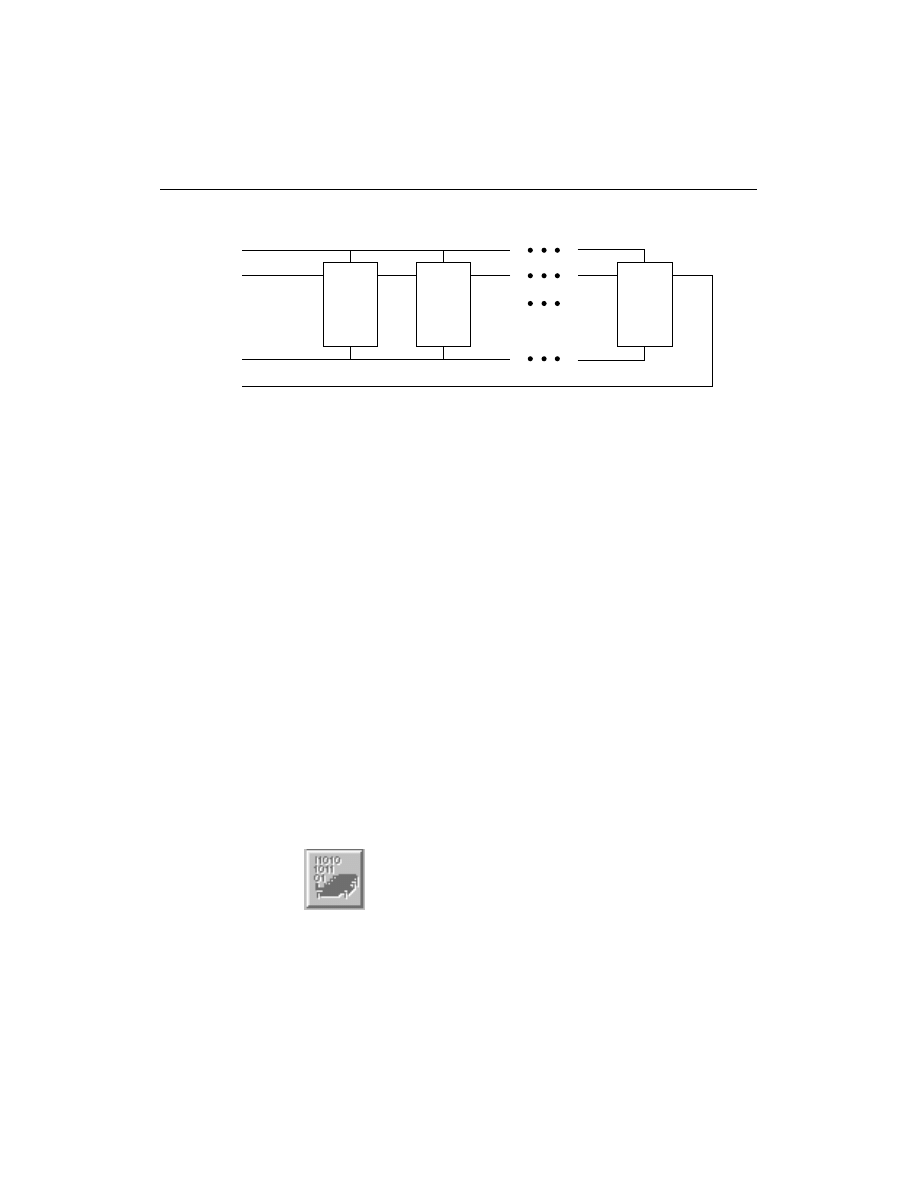
JTAG Programmer Tutorial
JTAG Programmer Guide
3-3
Figure 3-2
Device Chain
The chain description must contain all devices in the order that they
appear in the JTAG programming chain.
Alternatively, you can use the
Initialize Chain
operation to
automatically identify the devices in the system boundary-scan
chain. You must then associate JEDEC files for XC9500/XL/XV
CPLD devices, BIT files for Xilinx FPGA devices, and BSDL files for
all other devices by using the device properties dialog box.
Configuring a Device In-System
If you have created programming files (<
filename
>
.jed
) and are
ready to download them to XC9500/XL/XV devices in-system
through the JTAG chain, proceed as follows:
1.
Make sure the cable is attached properly and the target board is
turned on.
2.
Invoke the JTAG Programmer Download Software menu by
double-clicking the JTAG Programmer Download Software icon.
Figure 3-3
JTAG Programmer Icon
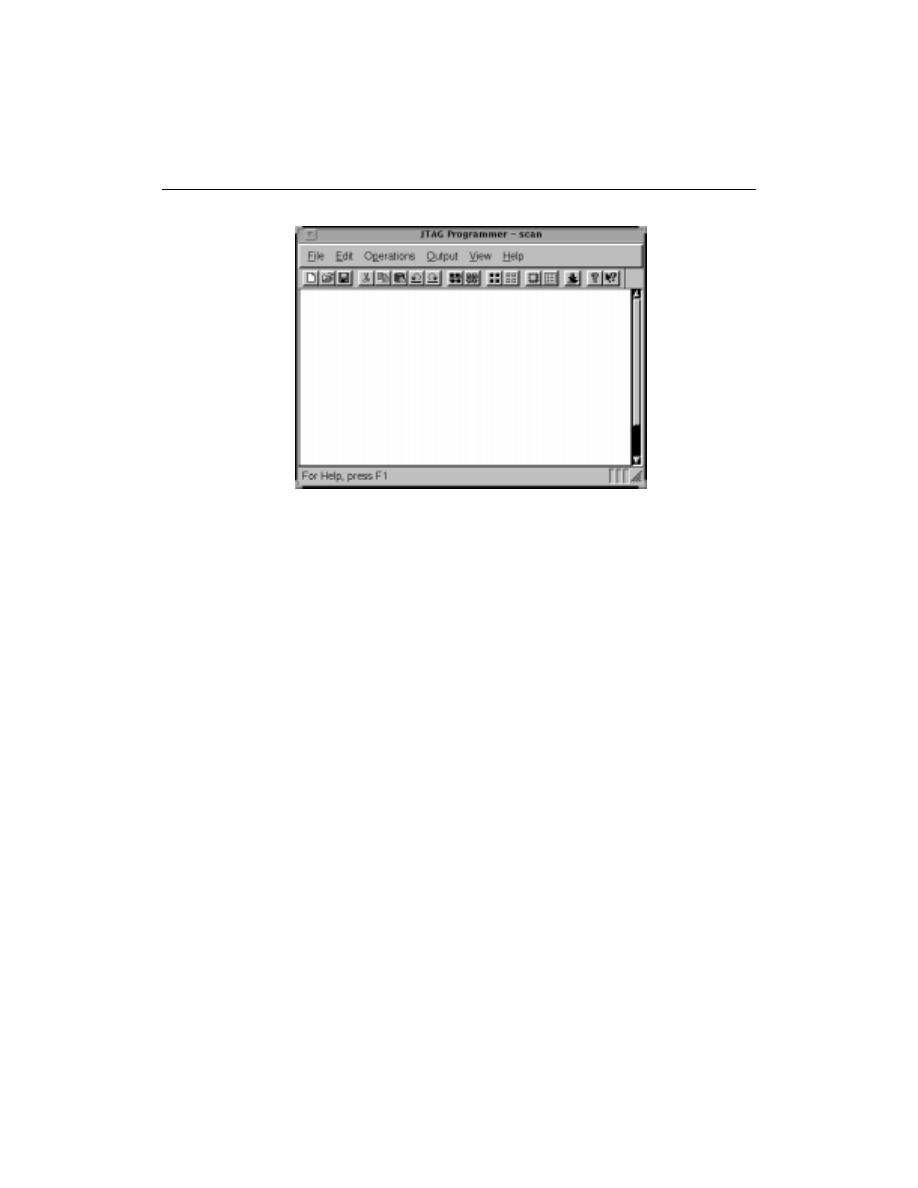
The JTAG Programmer will appear.
U1
TCK
U2
Un
TDI
TMS
TDO/RD
TDO
X8006
JTAG Programmer Guide
3-4
Xilinx Development System
Figure 3-4
JTAG Programmer
3.
Add a device for each part in your boundary-scan chain.
Edit
→
Add Device
Or, if you have the cable set up and connected to a boundary-scan
chain, you can use the automatic device identification feature of
the JTAG Programmer to display the entire chain. To do this:
File
→
Initialize Chain
The programmer goes out and finds all the parts in the chain,
identifies them, and displays them in the JTAG Programmer. If
the programmer finds a device it can’t identify, it displays the
device as an unknown part.
JTAG Programmer Tutorial
JTAG Programmer Guide
3-5
Figure 3-5
Automatic Device Identification
4.
You need to specify a JEDEC file for each XC9500/XL/XV device
in the boundary-scan chain, a BIT file for each Xilinx FPGA
device, and a BSDL file for all other devices in the boundary-scan
chain. Highlight the first device in the chain by clicking once on it
and then select the JEDEC or BSDL file corresponding to the
device.
Edit
→
Properties
Alternatively, you may double-click on the device icon.
The
Device Properties
dialog box appears
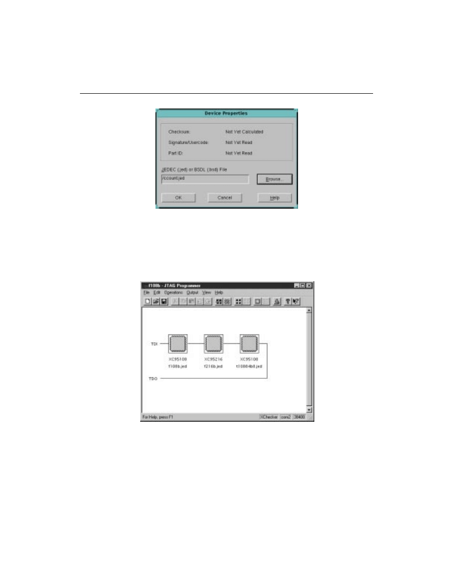
JTAG Programmer Guide
3-6
Xilinx Development System
Figure 3-6
Device Properties
5.
Type in the path name or click once on the browse key and find
the appropriate file to assign to the highlighted part. Select
JEDEC files for each XC9500/XL/XV device in the chain, BIT files
for each Xilinx FPGA device, and BSDL files for the remaining
devices. Repeat for each device in the chain.
Figure 3-7
Device Chain (unprogrammed)
JTAG Programmer Tutorial
JTAG Programmer Guide
3-7
Programming Xilinx CPLD and FPGA Devices
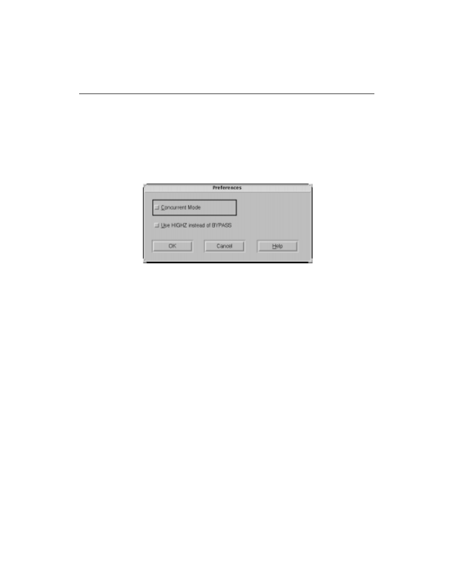
There are two preferences available that you may want to select
before initiating a session. They are
Concurrent Mode
and
Use
HIGHZ instead of BYPASS
. These options are selected as follows:
File
→
Preferences
The
Preferences
dialog box will appear.
Figure 3-8
Preferences
Concurrent Mode
The JTAG Programmer normally uses a sequential methodology
when accessing Xilinx CPLDs for ISP operations. It selects a device to
program and sets all other devices in the boundary-scan chain into
BYPASS mode. Concurrent Mode erases, programs and verifies
selected devices in the chain without placing these parts in BYPASS
mode. This has the advantage of saving time by executing operations
simultaneously.
For example, it takes few seconds to completely erase all the sectors
of a device. If you have several devices in a chain, these erase times
can add up. In concurrent mode the erasures can take place simulta-
neously, saving time.
Note:
Concurrent mode is applicable only to Xilinx CPLD devices.
Since Xilinx FPGA devices are SRAM based; their access method
precludes this kind of operation.
Use HIGHZ instead of BYPASS
The JTAG Programmer usually places parts in BYPASS mode when
other devices in the boundary-scan chain are being programmed.
JTAG Programmer Guide
3-8
Xilinx Development System
This option places XC9500/XL/XV devices in high impedance mode
instead. If you suspect that noise is degrading the integrity of ISP
operations, use this mode to reduce the signal activity level in the
system.
Note:
If you decide to use HIGHZ instead of BYPASS you must be
certain that your design can tolerate XC9500/XL/XV device pins
floating. If these pins connect to memory enable pins, for instance,
their floating values may inadvertently cause the devices to turn on,
potentially damaging their drivers or parts downstream from them.
Selecting Parts for Programming (Xilinx CPLD)
If your boundary-scan chain consists of only Xilinx CPLD devices,
then you can select all XC9500/XL/XV devices at once with
Edit
→
Select All
, or highlight each device individually, then:
Operations
→
Program
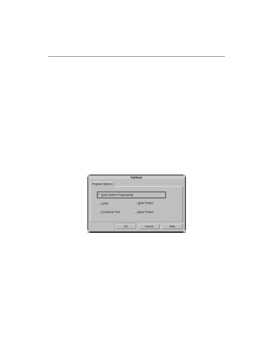
The program options box appears. Select the desired program-
ming options, then click
OK
.
Figure 3-9
Options
When the programming operation is complete, the programming
status of each Xilinx programmable device is reported as shown:
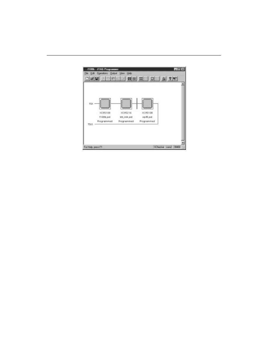
JTAG Programmer Tutorial
JTAG Programmer Guide
3-9
Figure 3-10
Programmed Chain
Selecting Parts for Programming (Xilinx FPGA)
If your boundary-scan chain consists of only Xilinx FPGA devices,
then you can select all Xilinx FPGA devices at once with
Edit
→
Select All
or highlight each device individually, then:
Operations
→
Program
The programming options box appears. Select the desired options,
then click
OK
.
Selecting Operations
There are two ways to set up the chain for JTAG Programmer opera-
tions. The first is to highlight a part and select an operation for it
using the
Operations
menu. You select an operation from the
menu, then highlight the next part and select an operation for it, or
you may highlight all parts and select an operation for all parts.
The other way is to use the Chain Operations dialog box. This
presents you with a “spreadsheet” approach to boundary-scan chain.
This method allows you select and execute operations for all the parts
in the chain, all from the same dialog box. To access this dialog box:
Operations
→
Chain Operations...
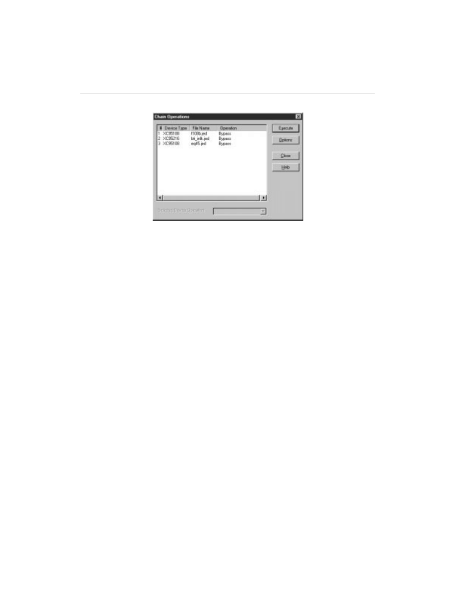
JTAG Programmer Guide
3-10
Xilinx Development System
Figure 3-11
Chain Operations
The dialog box appears. In the
Operations
column you may change
the operation of any part by clicking once on the current device to
highlight it, then clicking once on the down arrow adjacent to
Selected Device Operation
. This will produce a pull-down
menu showing the operations you can set for that part.
Note:
Bypass is the only supported mode of Operation for non-Fast-
FLASH parts. These parts will appear under Device Type. Note that
Bypass is selected as the default Operation of each foreign part.
Select the
Execute
button. Download will begin.
In either operation mode a pop-up menu appears and delivers
processing messages. When processing has completed, a message log
is available to examine the results of the execution.
Modifying a Chain
The Edit menu provides easy means for inserting and deleting parts
from a chain, as well as the means to assign a new JEDEC file to a
part.
Adding a Device
To insert a device into the chain, use the
Add Device
command.
First make sure that the prompt is at the location in the chain where
you want to insert the device. If it is not, use either the mouse or the
arrow keys to move it. Then insert the device as follows:

JTAG Programmer Tutorial
JTAG Programmer Guide
3-11
Edit
→
Add Device
Changing a Part
To change the jedec file associated with a device in the chain, high-
light the device and:
Edit
→
Properties
Use the browse key to select another jedec file or simply enter the
path and filename of the file. The program will associate the new file
with the device.
Note:
Each jedec assigns a device type to the device in the chain. If
the jedec file was not created for the actual device you have on your
board, an error will result when you attempt to program the device.
Deleting a Part
To delete an entry in the device chain, use the
Cut
command. All
devices move up one entry in the chain.
Edit
→
Cut
Selecting the Entire Chain
To select the entire chain for an operation, use
Edit
→
Select All
To unselect the chain:
Edit
→
Unselect All
Note:
When operating in SVF mode, chain modifications are not
allowed so as to ensure that the resulting SVF if self-consistent.
Saving the Chain Description
To save a JTAG Programmer chain description for later use, create a
Chain Description File (
.cdf
) using:
File
→
Save
If the chain has not been previously saved, the
Save As
dialog box
will appear. This screen will allow you to select a directory and path
to place the file in. You can also name the file, but you should retain
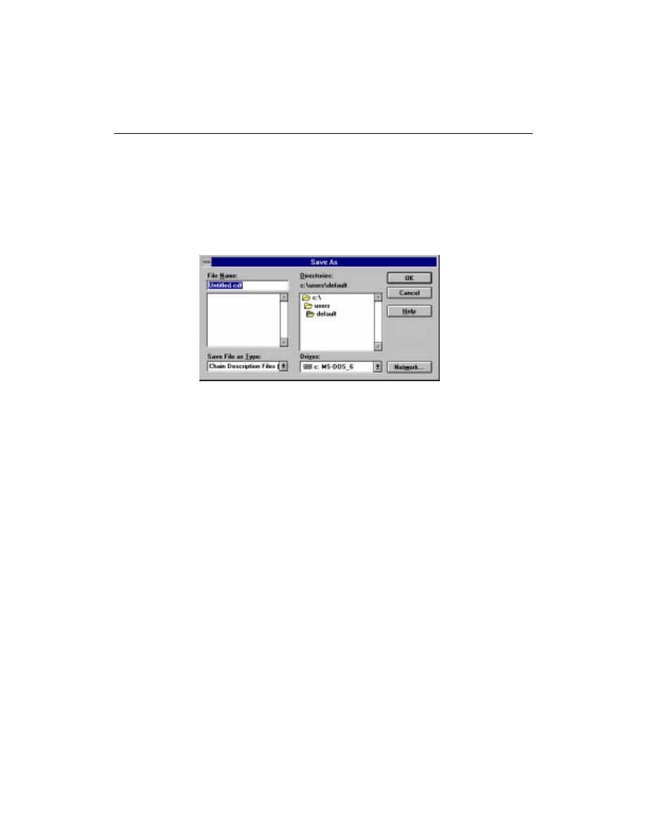
JTAG Programmer Guide
3-12
Xilinx Development System
the
.cdf
file extension. If you wish to save your file under another
name than already selected, use:
File
→
Save As...
To name your file, use the mouse to highlight Untitled or the old file
name on the File Name line, then type in the name you want and click
once on OK.
Figure 3-12
Saving a File
Debugging a Chain
The debugger provides you with a method to apply boundary-scan
test access port stimulus. This feature allows you to set TDI and TMS,
then pulse TCK a specified number times. You can monitor TDO, TDI
and TMS using an oscilloscope or logic probe to see if the boundary-
scan chain is operating correctly. The debugger also displays the
current TAP state and allows you to reset the chain to Run Test Idle.
To access the debugger:
File
→
Debug Chain
The Boundary-Scan Chain Debug dialog box appears as shown in
Figure 3-13.
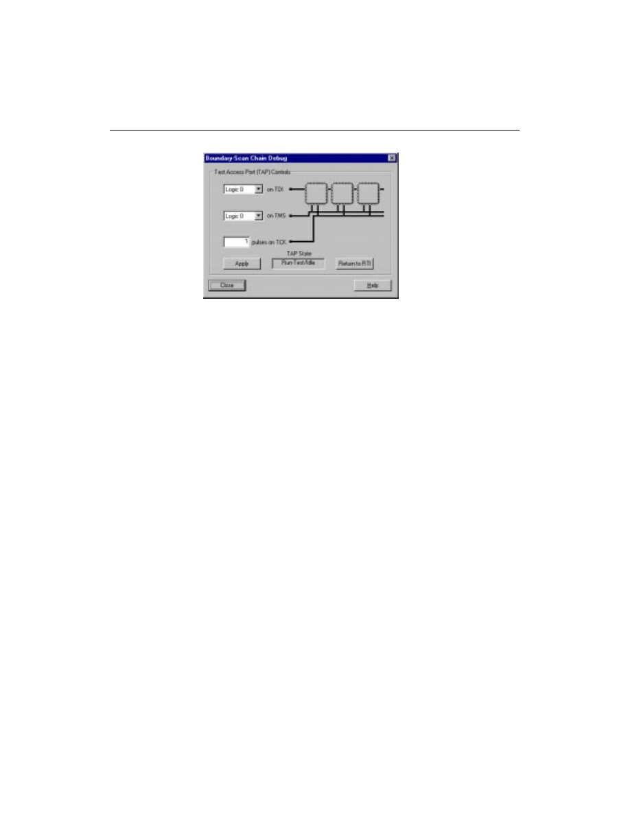
JTAG Programmer Tutorial
JTAG Programmer Guide
3-13
Figure 3-13
Debug
The features of this dialog box operate as follows:
•
The first selection box allows you to set a logic state for TDI. This
state will not be set until you click on the
Apply
button.
•
The second selection box allows you to set a logic state for TMS.
This state will not be set until you click on the
Apply
button.
•
The third selection box allows you to set a number of pulses to
apply to TCK. These pulses will not be sent until you click on the
Apply
button. If you want to see the pulses again, click the
Apply
button as often as you want.
•
The TAP State window displays the current state of the
controller.
•
The Return to RTI (Run Test Idle) button executes a Test Logic
Reset, then returns to Run Test Idle.
Data Security Selection
Any Xilinx CPLD device selected for programming can be secured
with the
Write Protect
or
Read Protect
or both.
When enabled,
Read Protect
disables reading the programmed
contents of a device (the
Device ID
and usercode/signature and
boundary scan register remain readable).
Write Protect
allows only the reading of the programmed data.
The device contents cannot be altered or re-programmed.
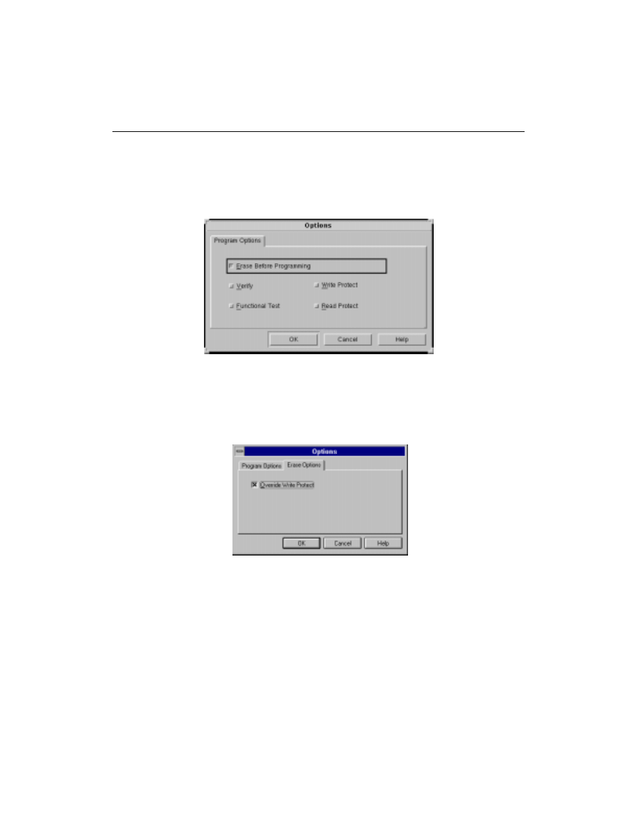
JTAG Programmer Guide
3-14
Xilinx Development System
When both
Read Protect
and
Write Protect
are enabled, the
device can be neither read nor re-programmed.
To enable either security function simply place a check in the corre-
sponding box when programming the device.
Figure 3-14
Data Selection (Program Options)
Data security operations can be overridden only by erasing the
device. For Read Protection override, you simply erase the part. For
Write Protection override, you must select the override write protect
option from the
Erase Options
dialog box.
Figure 3-15
Data Selection (Erase Options)
Generating SVF Files
Serial Vector Format (SVF) files are used when programming
XC9500/XL/XV devices on automatic test equipment (ATE). The
JTAG Programmer allows you to create
.svf
files for use with ATE
systems. To do this you need to create a new SVF file:
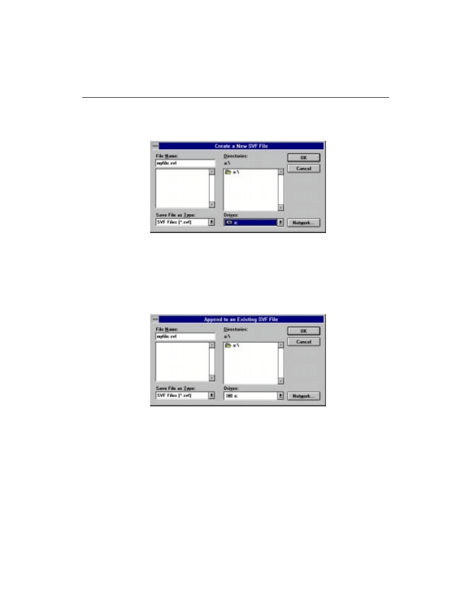
JTAG Programmer Tutorial
JTAG Programmer Guide
3-15
Output
→
Create SVF File...
The
Create a New SVF File
dialog box will appear.
Figure 3-16
Create an SVF File
Select a name and a directory to create the new file in, then click
OK
.
To append your vectors to an existing SVF file, use:
Output
→
Append to SVF File...
The
Append to an Existing SVF File
dialog box will appear.
Figure 3-17
Append to an SVF File
Select a file to append to and click
OK
.
Note:
Program, Verify, Erase, Functional Test, Get Device ID and Get
Signature/Usercode are allowed operations in SVF mode.
After identifying the SVF file to be used for collection of SVF data,
operate on the devices in your boundary-scan chain in the manner
described previously. Remember that in SVF mode, chain editing

JTAG Programmer Guide
3-16
Xilinx Development System
operations are not allowed to ensure that the resulting SVF file will be
self-consistent.
Xilinx provides software on the Xilinx Website that converts SVF files
into ATE vectors. Visit our site at
www.xilinx.com
for more infor-
mation.
Substituting with Version n Devices
If you generated SVF files for XC95108 or XC95216 Version 0 devices,
the files will work without modification on any later version devices.
If you wish, however, to take advantage of improved ISP capabilities
available on later version silicon devices, and you are certain that you
have such devices in your boundary-scan chain, then you can
generate version specific SVF files using the following techniques:
Using the Batch Tool (jtagprog)
Invoke the tool to generate SVF files:
jtagprog -svf
When specifying the part_type in the part command identify Version
1 silicon by appending “
_v
n
” to the part name (where
n
is the version
number device being used). For example, to specify a chain of Version
1 XC95216s and XC95108s:
part xc95216_v1:design216a xc95108_v1:design108
xc95216_v1:design216b
Next, specify operations as usual to generate the required SVF files.
Using the JTAG Programmer
In your $XILINX/data directory you will notice BSDL files with the
following names:
xc95108.bsd
xc95108_v1.bsd
xc95216.bsd
xc95216_v1.bsd
The BSDL files with the “_v1” in their names describe the Version 1
silicon. Similarly, those with “_v2” are for Version 2 devices. To get

JTAG Programmer Tutorial
JTAG Programmer Guide
3-17
the software to use Version 1 BSDL files for all devices, you must
“trick” the application by renaming files as follows:
1.
Rename xc95108.bsd to xc95108_v0.bsd
2.
Rename xc95216.bsd to xc95216_v0.bsd
3.
Rename xc95108_v1.bsd to xc95108.bsd
4.
Rename xc95216_v1.bsd to xc95216.bsd
Invoke the JTAG Programmer and set it to generate SVF files as
described earlier in this section. When you use the JTAG
Programmer, it will default to using the xc95216.bsd and xc95108.bsd
files to describe the parts. This will allow access to all Version 1
features.
When you are done programming, remember to change the file
names back so that the software will work correctly in non-SVF
modes:
1.
Rename xc95108.bsd to xc95108_v1.bsd
2.
Rename xc95216.bsd to xc95216_v1.bsd
3.
Rename xc95108_v0.bsd to xc95108.bsd
4.
Rename xc95216_v0.bsd to xc95216.bsd
JTAG Programmer Guide
4-1
Chapter 4
Designing Boundary-Scan and ISP Systems
This chapter gives design considerations for boundary-scan and ISP
systems. It contains the following sections:
•
“Connecting Devices in a Boundary-Scan Chain” section
•
“FPGA Device Considerations” section
•
“Bitstream Considerations” section
•
“Device Set-up” section
Connecting Devices in a Boundary-Scan Chain
All devices in the chain share the TCK and TMS signals. The system
TDI signal is connected to the TDI input of the first device in the
boundary-scan chain. The TDO signal from that first device is
connected to the TDI input of the second device in the chain and so
on. The last device in the chain has its TDO output connected to the
system TDO pin. This configuration is illustrated in Figure 4-1.
Figure 4-1
Single Port Serial Boundary-Scan Chain
U1
TCK
U2
Un
TDI
TMS
TDO/RD
TDO

JTAG Programmer Guide
4-2
Xilinx Development System
Design Rules for Boundary-Scan and ISP Systems
The boundary-scan standard requires pull-up resistance to be
supplied internally to the TDI and TMS pins by the chips, but no
particular value is required. This allows vendors supply whatever
they choose and still remain in full compliance. Because of this, very
long boundary-scan chains, or chains using parts from multiple
vendors, may present significant loading to the ISP drive cable. In
these cases:
1.
Use the latest Xilinx download cables (parallel cables with serial
numbers greater than 5000, or any X-Checker cable).
2.
Consider including buffers on TMS or TCK signals interleaved at
various points on your JTAG circuitry to account for unknown
device impedance.
Some users have noted that their designs appear to experience
erase time or programming time extension as the design
progresses, particularly for long chains. This is probably due to
switching noise.
3.
Put the rest of the JTAG chain into HIGHZ mode by selecting the
HIGHZ preference on JTAG Programmer when programming a
troublesome part.
This will limit the number of additional signals presented to the
system and the troublesome part.
4.
If free running clocks are delivered into boundary-scan devices, it
may be necessary to disconnect or disable their entry into these
devices during ISP or boundary-scan operations.
Charge pumps, the heart of the XC9500/XL/XV ISP circuitry,
require a modest amount of care. The voltages to which the
pumps must rise are directly derived from the external voltage
supplied to the VCCINT pins on the XC9500/XL/XV parts.
Because these elevated voltages must be within their prescribed
values to properly program the CPLD, it is vital that they be
provided with very clean (noise free) voltage within the correct
range. This suggests the first two key rules:
5.
Make sure VCC is within the rated value: 5V +/- 5%.
6.
Provide both 0.1 and 0.01 uF capacitors at every VCC point of the
chip, and attached directly to the nearest ground.

Designing Boundary-Scan and ISP Systems
JTAG Programmer Guide
4-3
FPGA Device Considerations
JTAG Programmer supports the configuration of Xilinx FPGA
devices through the boundary-scan test access port (TAP). In order to
enable boundary-scan-based configuration capabilities for FPGA
devices, you must design your systems and prepare your configura-
tion bitstreams in the following manner.
Bitstream Considerations
JTAG Programmer only accepts FPGA configuration files in the
binary bitstream format (.bit). It does not allow configuration using
the ASCII raw bits (.rbt) format.
Note:
Express mode bitstreams cannot be used to configure devices
via boundary-scan.
Make certain that the boundary-scan (BSCAN) symbol has been
included in your design. If it has not then the bitstream will also not
be usable for boundary-scan based configuration. Standard examples
for instantiating the BSCAN symbol in FPGAs are included in
Appendix F.
Keep your device bitstream files separate for each device in the
boundary-scan chain. JTAG Programmer requires you to assign a
single bit file to each device. It cannot manipulate composite bit files.
Device Set-up
Xilinx recommends that all the mode pins of the devices be tied low
before starting the configuration. This is recommended for all
XC4000, XC5000 and Spartan device families.
In order to enable the boundary-scan circuitry in the device, you
must install a pull down resistor on the INIT pin. The value of the
pull down should be selected so as to draw the INIT pin to approxi-
mately 0.5V. Typically a pull down of approximately 1KOhm should
accomplish this.
Verifying Device Configuration
The XC4000 (not the XLA and XV), XC5000 and Spartan (not the
SpartanXL) devices freeze if data errors occur during boundary-scan
configuration. The only method for unlocking the frozen device is to

JTAG Programmer Guide
4-4
Xilinx Development System
reset the power to the device or pulse the PROGRAM pin low. (This
latter method would have to be accomplished manually since the
download cables (when being used for boundary-scan operations),
do not have control over the PROGRAM pin. Although this situation
is rare, it is possible to design your system so as to detect if that condi-
tion has occurred. The JTAG Programmer software allows you to
check for this in three ways:
1. Assume successful verification - since it is a low probability event,
simply configure the device and run. The drawback is that the failure
of the device is then only detected at run-time.
2. Readback verify the configuration memory - after configuring,
readback the contents of the configuration memory and check against
the source bitstream file. If the device has frozen, the returned bits
will be incorrect. Since bit files can be large, this might be time
consuming.
3. Tie a free pin on the device to ground - after configuring, the soft-
ware will perform an EXTEST instruction to read the device pin
value. If the device has locked up, the pin value will not be read
correctly.
Device Behavior Notes
Any verify operation executed immediately after configuration
without boundary-scan functionality enabledwill fail because the test
access port no longer exists. Always remember to instantiate the
BSCAN symbol for reliable operation of your devices.
The implementation of boundary-scan based configuration of FPGAs
precludes the use of concurrent ISP. For this reason, the concurrent
mode preference is disabled (or ignored) when FPGAs are selected to
be operated upon.

Boundary Scan Basics
A-1
Appendix A
Boundary Scan Basics
Boundary Scan
What is IEEE 1149.1?
Design complexity, difficulty of loaded board testing, and the limited
pin access of surface mount technology led industry leaders to seek
accord on a standard to support the solution of these problems.
JTAG Boundary Scan, formally known as IEEE Standard 1149.1, is
primarily a testing standard created to alleviate the growing cost of
designing and producing digital systems. The primary benefit of the
standard is the ability to transform extremely difficult printed circuit
board testing problems (that could only be attacked with ad-hoc
testing methods) into well-structured problems that software can
handle easily and swiftly.
The standard defines a hardware architecture and the mechanisms
for its use to solve the aforementioned problems.
What can it be used for?
Although primarily a testing standard for on-chip circuitry, the prolif-
eration of the standard has opened the door to a wide variety of
applications. The standard itself defines instructions that can be used
to perform functional and interconnect tests as well as built-in self
test procedures.
Vendor-specific extensions to the standard have been developed to
allow execution of maintenance and diagnostic applications as well
as programming algorithms for reconfigurable parts. It is the latter
that have been implemented (in addition to all the mandatory opera-

Boundary Scan Basics
A-2
Xilinx Development System
tions of the standard and some optional ones) in the FastFLASH
family.
How does it work?
The top level schematic of the test logic defined by IEEE Std 1149.1
includes three key blocks:
The TAP Controller
This responds to the control sequences supplied through the test
access port (TAP) and generates the clock and control signals
required for correct operation of the other circuit blocks.
The Instruction Register
This shift register-based circuit is serially loaded with the instruction
that selects an operation to be performed.
The Data Registers
These are a bank of shift register based circuits. The stimuli required
by an operation are serially loaded into the data registers selected by
the current instruction. Following execution of the operation, results
can be shifted out for examination.
The JTAG Test Access Port (TAP) contains four pins that drive the
circuit blocks and control the operations specified. The TAP facilitates
the serial loading and unloading of instructions and data. The four
pins of the TAP are: TMS, TCK, TDI and TDO. The function of each
TAP pin is as follows:
TCK
- this pin is the JTAG test clock. It sequences the TAP controller
as well as all of the JTAG registers provided in the XC95108.
TMS
- this pin is the mode input signal to the TAP Controller. The
TAP controller is a 16-state FSM that provides the control logic for
JTAG. The state of TMS at the rising edge of TCK determines the
sequence of states for the TAP controller. TMS has an internal pull-up
resistor on it to provide a logic 1 to the system if the pin is not driven.
TDI
-this pin is the serial data input to all JTAG instruction and data
registers. The state of the TAP controller as well as the particular
instruction held in the instruction register determines which register
is fed by TDI for a specific operation. TDI has an internal pull-up

Boundary Scan Basics
Boundary Scan Basics
A-3
resistor on it to provide a logic 1 to the system if the pin is not driven.
TDI is sampled into the JTAG registers on the rising edge of TCK.
TDO
- this pin is the serial data output for all JTAG instruction and
data registers. The state of the TAP controller as well as the particular
instruction held in the instruction register determines which register
feeds TDO for a specific operation. Only one register (instruction or
data) is allowed to be the active connection between TDI and TDO for
any given operation. TDO changes state on the falling edge of TCK
and is only active during the shifting of data through the device. This
pin is three-stated at all other times
JTAG TAP Controller
The JTAG TAP Controller is a 16-state finite state machine, that
controls the scanning of data into the various registers of the JTAG
architecture. The state of the TMS pin at the rising edge of TCK is
responsible for determining the sequence of state transitions. There
are two state transition paths for scanning the signal at TDI into the
device, one for shifting in an instruction to the instruction register
and one for shifting data into the active data register as determined
by the current instruction.
JTAG TAP Controller States
Test-Logic-Reset
. This state is entered on power-up of the device
whenever at least five clocks of TCK occur with TMS held high. Entry
into this state resets all JTAG logic to a state such that it will not inter-
fere with the normal component logic, and causes the IDCODE
instruction to be forced into the instruction register.
Run-Test-Idle
. This state allows certain operations to occur
depending on the current instruction. For the XC9500/XL/XV family,
this state causes generation of the program, verify and erase pulses
when the associated in-system programming (ISP) instruction is
active.
Select-DR-Scan
. This is a temporary state entered prior to
performing a scan operation on a data register or in passing to the
Select-IR-Scan state.
Select-IR-Scan
. This is a temporary state entered prior to performing
a scan operation on the instruction register or in returning to the Test-
Logic-Reset state.

Boundary Scan Basics
A-4
Xilinx Development System
Capture-DR
. This state allows data to be loaded from parallel inputs
into the data register selected by the current instruction on the rising
edge of TCK. If the selected data register does not have parallel
inputs, the register retains its state.
Shift-DR
. This state shifts the data, in the currently selected register,
towards TDO by one stage on each rising edge of TCK after entering
this state.
Exit1-DR
. This is a temporary state that allows the option of passing
on to the Pause-DR state or transitioning directly to the Update-DR
state.
Pause-DR
. This is a wait state that allows shifting of data to be
temporarily halted.
Exit2-DR
. This is a temporary state that allows the option of passing
on to the Update-DR state or returning to the Shift-DR state to
continue shifting in data.
Update-DR
. This state causes the data contained in the currently
selected data register to be loaded into a latched parallel output (for
registers that have such a latch) on the falling edge of TCK after
entering this state. The parallel latch prevents changes at the parallel
output of these registers from occurring during the shifting process.
Capture-IR
. This state allows data to be loaded from parallel inputs
into the instruction register on the rising edge of TCK. The least two
significant bits of the parallel inputs must have the value 01 as
defined by IEEE Std. 1149.1, and the remaining 6 bits are either hard-
coded or used for monitoring of the security and data protect bits.
Shift-IR
. This state shifts the values in the instruction register
towards TDO by one stage on each rising edge of TCK after entering
this state.
Exit1-IR
. This is a temporary state that allows the option of passing
on to the Pause-IR state or transitioning directly to the Update-IR
state.
Pause-IR
. This is a wait state that allows shifting of the instruction to
be temporarily halted.
Exit2-IR
. This is a temporary state that allows the option of passing
on to the Update-IR state or returning to the Shift-IR state to continue
shifting in data.

Boundary Scan Basics
Boundary Scan Basics
A-5
Update-IR
. This state causes the values contained in the instruction
register to be loaded into a latched parallel output on the falling edge
of TCK after entering this state. The parallel latch prevents changes at
the parallel output of the instruction register from occurring during
the shifting process.
JTAG Instructions Supported in FastFLASH Parts
JTAG Programmer software uses sequences of these JTAG instruc-
tions to perform programming and verification operations selected
by the user. However, execution of individual JTAG instructions is
not supported by this software.
Mandatory Boundary Scan Instructions
BYPASS
. The BYPASS instruction allows rapid movement of data to
and from other components on a board that are required to perform
test operations.
SAMPLE/PRELOAD
. The SAMPLE/PRELOAD instruction allows a
snapshot of the normal operation of a components to be taken and
examined. It also allows data values to be loaded onto the latched
parallel outputs of the boundary scan shift register prior to the selec-
tion of other boundary-scan test instructions.
EXTEST
. The EXTEST instruction allows testing of off-chip circuitry
and board level interconnections.
Optional Boundary Scan Instructions
INTEST
. The INTEST instruction allows testing of the on-chip system
logic while the components are already on the board.
HIGHZ
. The HIGHZ instruction forces all drivers into high imped-
ance states.
IDCODE
. The IDCODE instruction allows blind interrogation of the
components assembled onto a printed circuit board to determine
what components exist in a product.
USERCODE
. The USERCODE instruction allows a user-program-
mable identification code to be shifted out for examination. This
allows the programmed function of the component to be determined.

Boundary Scan Basics
A-6
Xilinx Development System
FastFLASH Reconfiguration Instructions
ISPEN
. The ISPEN instruction activates the FastFLASH part for in-
system programming.
FPGM
. The FPGM instruction is used to program the fuse locations
at a specified address.
FERASE
. The FERASE instruction is used to perform an erase of a
block of fuse locations.
FVFY
. The FVFY instruction is used to read the programming of the
fuse locations at a specified address.
ISPEX
. The ISPEX instruction loads the programmed values into the
device memory. It then activates the device to operate according to
the programmed values.
FPGMI
. The FPGMI instruction is used to program fuse locations
sequentially from a preset starting address.
FVFYI
. The FVFYI instruction is used to read the programming of
fuse locations sequentially for a preset starting address.
FBULK
. The FBULK instruction is used to perform an erase of either
all function blocks or all Fastconnect blocks of a device.

JTAG Download Cable Schematics
B-1
Appendix B
JTAG Parallel Download Cable Schematic
This appendix contains a schematic of the Parallel Download Cable.
It is included in case you want to build your own download cables.
schematic, Figure B-1, is our current version of the Parallel Download
Cable. If you want to build a parallel cable, this is the recommended
schematic.
Note:
You must use recommended lengths for parallel cables. Xilinx
cables are typically six feet (about two meters) in length.
JTAG Download Cable Schematics
B-2
Xilinx Development System
Figure B-1
Parallel Download Cable
VCC SENSE
VCC
GND
TCK
TDI
TDO
TMS
VCC
GND
CCLK
D/P
DIN
PROG
1
2
4
7
6
9
1
2
3
4
5
5
3
6
7
8
9
8
100
100
100
100
100
100pF
100pF
100pF
100pF
5.1K
1K
.01uF
1N5817
X7557
JTAG Header
DB25 MALE
CONNECTOR
FPGA Header
100
300
300
300
300
300
DONE
PROG
DIN
TMS_IN
CTRL
CLK
GND
GND
D6
BUSY
PE
SHIELD
15
13
U1
14
7
3
2
5
12
9
1
6
4
11
13
8
10
U1
U1
U1
U1
6
2
4
5
3
20
25
8
11
12
U2
U2
U2
U1 = 74HC125
U1 = 74HC125
Serial JT -05000 and above
for EPP parallel ports.
100
U2
1
1N5817
U2
14
7
2
6
5
8
4
9
10
12
11
13

Troubleshooting
C-1
Appendix C
Troubleshooting Guide
This chapter is a simple guide to understanding the more common
issues you might encounter when configuring CPLDs with JTAG
Programmer. These issues are likely to fall into three groups; commu-
nication, improper connections, and improper or unstable V
CC
.
•
“Communication” section
This section describes several issues that involve the integrity of
the bitstream that JTAG Programmer transmits to the target
CPLDs, and the correct connection of the boundary-scan chain.
•
“Improper Connections” section
This section involves assigning configuration pins to invalid
signals or voltage levels.
•
“Improper or Unstable VCC” section
This section describes several causes of incorrect configuration
sequences and incorrect responses from the target system.
•
“Boundary Scan Chain Errors” section
If you experience a consistent error that identifies a break in your
boundary-scan chain, go to this section.
•
“System Noise” section
If you experience intermittant problems characteristic of system
noise, go to this section.
Communication
Observing the following guidelines should minimize the communi-
cation difficulties that can occur between the cable hardware and the
target system.

Troubleshooting
C-2
Xilinx Development System
Do not attach extension cables to the target system side of the cable;
this can compromise configuration data integrity and cause
checksum errors.
Attach the cable configuration leads firmly to the target system.
After connecting the target system, specify the chain configuration
using the
part
command. Then use the "
partinfo -id
part_name"
command to read the IDCODE from each part in the system. This will
verify the integrity of the boundary-scan chain. If you are using the
Graphical User Interface:
Operations
→
Get Device ID
Use the verify feature to assure integrity of the configuration data.
You can do this from the command line with the –v option or in the
interactive mode by specifying the verify command.
When using the JTAG Programmer software with the cable on a PC to
download, the process may stop with data communications errors.
This is caused by serial port communication inefficiencies in the
Windows environment. To set your PC to better handle serial
communications at 38400 baud, add (or modify) the following lines to
the 386Enh section of your SYSTEM.INI file. This file is located in the
Windows directory of your system.
COM1Buffer=32768
COM2Buffer=32768
COMBoostTime=10240
Improper Connections
Always make sure that cable leads are connected properly.
Note:
Connecting the cable leads to the wrong signal will cause
permanent damage to cable internal hardware. You must connect
V
CC
to +5 V and GND to ground.
For workstations, you must have read and write permissions to the
port to which you connect the cable. JTAG Programmer might issue a
message stating that the cable is not connected to port ttyx. When you
see this message, follow the check list below:
•
The board must have the power on, since the cable uses power
from the board.

Troubleshooting Guide
Troubleshooting
C-3
•
Check the device driver using the following command string:
ls –l /dev/ttya /dev/ttyb
The result should be the following:
crw-rw-rw- 1 root12,0
month date time /dev/ttya
crw-rw-rw- 1 root12,1
month date time /dev/ttyb
•
Reconnect the cable to another valid port.
•
Read the /etc/ttytab file. There should be two lines, as follows:
ttya‘‘/usr/etc/getty std.9600’’ unknown off local
secure
ttyb‘‘/usr/etc/getty std.9600’’ unknown off local
secure
If you use a port to connect a modem or a remote login, you cannot
use that port. The port must be on. Consult your System Adminis-
trator if the information the /etc/ttytab file is different than what is
listed in the aforementioned list.
Improper or Unstable V
CC
Never connect the control signals to the cable before V
CC
and ground.
Xilinx recommends the following sequence:
1.
Turn off power to the target system.
2.
Connect V
CC
ground, and then the signal leads,
3.
Turn on power to the target system.
Warning:
The XChecker Cable has an internal FPGA. As with any
CMOS device, the input/output pins of the internal FPGA should
always be at a lower or equal potential than the rail voltage to avoid
internal damage.
Make sure V
CC
rises to a stable level within 10ms. Stable V
CC
should
be between 4.75 V and 5.25 V.
In the event of power glitches, reset the cable by selecting:
Output
→
Cable Reset

Troubleshooting
C-4
Xilinx Development System
Boundary Scan Chain Errors
If you experience a consistent error that identifies a break in your
boundary-scan chain but are unable to identify such a discontinuity
then execute the following steps:
1.
Create a command file to be used with the batch version of the
JTAG Programmer (
jtagprog
). In this batch file specify your
boundary-scan chain configuration using the
part
command
and about 50 idcode queries as follows:
part xc9572:design72 xc95108:design108
partinfo -id design108
partinfo -id design108
partinfo -id design108
.
.
.
partinfo -id design108
quit
2.
Save the file as
test.cmd
and then invoke the tool as follows:
jtagprog -batch test
3.
The tool will execute the device id command 50 times before quit-
ting. While this is going on use the oscilloscope to probe the pins
of the boundary scan test access port (TAP) at the system entry
point and at each individual part.
The boundary scan integrity check sequences the TAP through a
TRST sequence (TMS set to 1, TCK pulsed 5 times) and then tran-
sitions all devices to the RunTest/Idle state (TMS set to 0, TCK
pulsed once). Then, all parts are run through a CAPTURE -IR
sequence while TDI is set to 1 (1s will be shifted in). If you look in
the device BSDL files you will see the expected capture sequence
defined in the “instruction capture” field. For all XC9500/XL/XV
parts this sequence is a “1” followed by seven zeros. You should
therefore see the “1” on TDO after the falling edge of the 4th TCK
pulse after the TRST sequence. On the next TCK pulse TDO
should return to zero.

Troubleshooting Guide
Troubleshooting
C-5
The CAPTURE -IR sequence consists of the following (starting
from RunTest/Idle), as illustrated in Figure C-1.
1.
TMS set to 1; TCK pulsed twice.
2.
TMS set to 0; TCK pulsed twice.
3.
TCK pulsed (number of bits in instruction register -1) times.
4.
TMS set to 1; TCK pulsed twice.
5.
TMS set to 0; TCK pulsed once.
Figure C-1
Sample Expected Waveform
Check for the following:
•
The expected number of TCK pulses occur.
•
The same TMS sequence occurs for each part.
•
The TDO is not shorted or floating between parts, or floating at
the system interconnect point.
•
Make certain that all 4 TAP signals are getting into each part
(Note that both TDI and TMS have internal pull-ups on them
which could keep the device in TRST mode if TMS is not prop-
erly connected).
You may also use the
Debug Chain
dialog and a logic probe or oscil-
loscope to transition the TAP state machine directly and observe
results.
1
0
0
0
0
0
0
0
1
0
0
0
0
0
0
2
3
4
5
6
7
8
YS "1"
X8083
2
3
4
5
6
7
8
1
1
1
0
0
0
0
0
0
0
1
0
0
0
0
0
0
2
3
4
5
6
7
8
YS "1"
X8083
2
3
4
5
6
7
8
1
1

Troubleshooting
C-6
Xilinx Development System
System Noise
You can check for system noise by running the IDCODE instruction
repeatedly. The IDCODE should read correctly 100% of the time. If by
test you find that the instruction is working less than 100% of the
time, you may be experiencing system noise.
To remedy a problem with system noise, select Use
HIGHZ instead
of BYPASS
from the Preferences dialog box. This places devices into
tri-state mode and reduces susceptibility to system noise. To find this
box use:
File
→
Preferences
The Preferences dialog box will appear. Place a check in the box adja-
cent to
Use HIGHZ instead of BYPASS
.

JTAG Programmer Guide
D-1
Appendix D
Error Messages
This section describes the error messages that JTAG Programmer may
generate. Following each error message, there is a suggested
workaround.
Error Messages
Command file
bat file.cmd
is not found.
Make sure that the command file you specified is in the current direc-
tory or the environment search path. Make sure that the command
file has the ".cmd" extension
Internal Error — Command table syntax error
Cmd=valid_command.
This is an internal program error that normally should not occur. Try
entering the command sequence again. If the error persists, try rein-
stalling your JTAG Programmer software. If the error reappears, call
Xilinx Technical Support. Be prepared to duplicate the error and
reference specific files or examples.
Cannot open output file
file_name
.
Check available disk space. Current directory or file must have write
permission.
Cannot create output file
file_name
.
Check available disk space. Current directory or file must have write
permission.
Cannot open input file
file_name
.
Make sure the file_name file exists in your working directory or in the
environment search path. Current directory or file must have write
permission.

Error Messages
D-2
Xilinx Development System
File
file_name
is not found.
The file_name file does not exist in the current directory or search
path. Make sure that the file_name file exists in your working direc-
tory or in the environment search path.
Help file
jtagprog.hlp
is not accessible
Make sure that the XILINX environment variable points to the instal-
lation directory in the PC. Also make sure that jtagprog.hlp is in the
installation\MSG directory. If you cannot find jtagprog.hlp in the
installation\MSG directory, you must reinstall the JTAG Programmer
software.
No help for command
command entered.
Help is not available for the specified command. Refer to the Interac-
tive Mode Commands section in Appendix E for help.
Cannot save configuration to
file_name.pro.
Check available disk space. Current directory or file must have write
permission.
Invalid command at line
line number.
Check the file xchecker.pro in your current directory for illegal
commands. Delete the xchecker.pro file. JTAG Programmer creates a
new profile when you exit from the session.
Ambiguous command.
Enter the minimum unique characters that identify the command or
enter complete commands with no abbreviations.
Invalid command.
The command you entered is illegal. Refer to the Interactive Mode
Commands section in Appendix E for help.
Invalid number of arguments.
Refer to the Interactive Mode Commands section in Appendix E for
help.
Invalid option
selected option.
Refer to the Command-Line Options and the Interactive Mode
Commands sections in Appendix E for help.
Invalid value given to
parameter.

Error Messages
JTAG Programmer Guide
D-3
Refer to the Command-Line Options and the Interactive Mode
Commands sections in Appendix E for help.
Value is required for
command entered.
Refer to the Interactive Mode Commands section in Appendix E for
help.
System Error Messages
System error codes are usually a string of messages generated by
your operating system.
System file error code.
System error codes are usually a string of messages generated by
your operating system.
Cable is not initialized.
Reissue the Reset command with the –c option, or cycle power to the
XChecker cable and then issue the Reset command with the –c
option. See the Improper or Unstable V
CC
section in Appendix E.
Cable is not located.
No cable has been recognized at any port. Make sure there is power
to your board and to the XChecker cable. If you are using the test
fixture, you must connect V
CC
and ground to it. The XChecker cable
draws power from your target system, not from your host computer.
Also make sure the RS-232 connector is firmly attached.
Invalid port name.
Refer to the XChecker Hardware section in Appendix E for help.
Invalid baud specified.
Refer to the XChecker Hardware section in Appendix E for help.
Cable is not reset.
Cycle power to the cable. Use the Reset command with the –c option.
Communication line is broken.
Run the Reset command with the –c option. Also make sure there is
power to your board and to the XChecker cable. Check all power and
port connections.
Communication checksum error.

Error Messages
D-4
Xilinx Development System
Check for induced noise in your target system or from your target
system into the XChecker connections. Do not use cable extensions.
The XChecker cable length is tested to produce minimal noise levels.
Remember that a logic High must be 80-100% of V
CC
and a Logic
Low must be 0-25% of V
CC
.
Cable has no power.
Make sure there is power from your target system to the XChecker
cable. The cable draws power from an external source, not from the
host computer.
Communication time-out.
JTAG Programmer has not received an expected signal; for example,
a system trigger to initiate readback or data coming from readback.
Make sure that the selected options for trigger and readback are what
you intended. Check all connections.
Cannot communicate to the cable.
Run the Reset command with the –c option. Also, ensure that there is
power to your board and to the XChecker cable. Check all connec-
tions. Make sure the RS-232 connector is firmly attached.
Cable datafile
file_name
is empty.
Run the Reset command with the –c option. Make sure that the
XILINX environment variable points to the installation directory on
the PC.
No XChecker cable is connected to the port
portname.
Ensure that there is power to your board and to the XChecker cable.
You must connect V
CC
and ground to the test fixture, if you are using
it. The cable draws power from your target system, not from the host
computer. Ensure that the RS-232 connector is firmly attached.
No XChecker cable is connected to the system.
Ensure that there is power to your board and to the cable. You must
connect V
CC
and ground to the test fixture, if you are using it.
XChecker draws power from your target system, not from the host
computer. Ensure that the RS-232 connector is firmly attached.
Fail reading cable status.
Try using the Reset command with the cable option. Ensure that there
is power to your board and to the cable. Check all connections.

Error Messages
JTAG Programmer Guide
D-5
Unsupported command for this cable.
See the Interactive Mode Commands section for valid with the
XChecker cable. If you are using the previous parallel or serial
download cables, you can only use the Load command to download.
Read only
number of bits received.
Check all connections. Check for noise that may be induced into your
target system or from your target system into the XChecker connec-
tions. Do not use cable extensions. The XChecker cable length is
tested to produce minimal noise levels. Remember that a logic High
must be 80-100% of V
CC
and a Logic Low must be 0-25% of V
CC
.
Invalid baud rate. Current baud rate is
baud rate.
See Table 2-1 for the valid baud rates for your computer.
Missing baud rate. Current baud rate is
baud rate.
See the Interactive Mode Commands section in Appendix E for
correct command usage.
Cannot communicate with port
port name.
Check this manual for supported ports. See the Port command.
Invalid port name
port name.
Refer to Table E-3 for supported ports. See the Port command.
Datafile
file_name
is empty.
The specified datafile is either empty or contains invalid data. JTAG
Programmer supports only JEDEC 3-C format.
Datafile
file_name
is not found.
The file_name file does not exits in the current directory or search
path. Check your environment search path to make sure that it
contains the directory where file_name is.
Can’t open datafile
file_name.
The file file_name does not exits in the current directory or search
path. Check your environment search path to make sure that it
contains the directory where file_name is located.
No part type is defined.

Error Messages
D-6
Xilinx Development System
The part type specified in your design or by you (using the Part
command) is invalid. Check the The Programmable Logic Data Book for
valid part types and packages.
Unable to execute erase command at address
string of
instance
string.
The specified device instance could not be erased. Check if data
protect is enabled as this disables the erase functionality. Also check
for the integrity of the cable connections.
Unable to program all addresses of instance
string.
The specified device instance could not be programmed. Check if
data protect or data security is enabled as this disables the program-
ming functionality. If data security is enabled, first issue an “erase”
command then execute the program command. Also check for the
integrity of the cable connections.
Verification of instance
string against program file
string failed.
The specified device instance could not be verified. Check if data
security is enabled as this disables the readback functionality. If this is
not the case, check for the integrity of the cable connections. If error
persists you may have a bad part and Xilinx customer service should
be contacted.
Unable to program address
string of instance string
with data
string.
The specified device instance could not be programmed. Check if
data protect or data security is enabled as this disables the program-
ming functionality. If data security is enabled, first issue an “erase”
command then execute the program command. Also check for the
integrity of the cable connections.
Unable to verify address
string of instance string
against data
string.
The specified device instance could not be verified. Check if data
security is enabled as this disables the readback functionality. If this is
not the case, check for the integrity of the cable connections. If error
persists you may have a bad part and Xilinx customer service should
be contacted.
Verification failed at address
value of instance
string. Expected:
value. Read: value.

Error Messages
JTAG Programmer Guide
D-7
The specified device instance could not be verified. Check if data
security is enabled as this disables the readback functionality. If this is
not the case, check for the integrity of the cable connections. If error
persists you may have a bad part and Xilinx customer service should
be contacted.
A description for a device named string has not been
supplied. Please make sure that a BSDL description was
loaded for this device.
A description for an instance named string of any
device has not been supplied. Please make sure that a
JTAG connection description was supplied for this
device.
Check that the specified part exists in the boundary-scan chain that
you declared in your “part” command. A new “part” command will
override the previously specified one. The current “part” database
can be displayed by typing “part” followed by a carriage return.
The boundary scan chain instruction register bit
sequence is incorrect at bit
value. This corresponds
to a scan chain break at or near part string.
Verification of the integrity of the boundary-scan chain failed. Check
cable connections and “part” command specification The current
“part” database can be displayed by typing “part” followed by a
carriage return.
In a multi-part boundary scan chain, the name of the
particular boundary scan part instance on which to
operate must be specified. Please retry this command
with an instance name specified.
You must specify a particular instance upon which to operated.
Respecify the command with that information. That is, specify “erase
instanceName” and not “erase”.
Unable to execute erase command for instance
string
The specified device instance could not be erased. Check if data
protect is enabled as this disables the erase functionality. Also check
for the integrity of the cable connections.
Unable to execute functional test command using
vectors in JEDEC file string.
Functional test vectors failed for instance string.

Error Messages
D-8
Xilinx Development System
Functional test vector
value failed for instance
string at pin number value. Expected output value:
value Actual output value: value
When running functional test using the INTEST instruction, the
applied functional vectors mismatched the predicted values. This
can be either a functional error in the design or an error in the vectors
specified. This will also occur when vectors targetted for a different
design are applied. Re-check the integrity of your design database
information.
Mismatched address values during verification of
instance
string. Check JEDEC file and cable
connections. Expected addressvalue:
value. Read:
value.
The specified device instance could not be verified. Check if data
security is enabled as this disables the readback functionality. If this is
not the case, check for the integrity of the cable connections. If error
persists you may have a bad part and Xilinx customer service should
be contacted.
Illegal IDCODE read from device identification
register on instance
string. IDCODE value: string
The IDCODE read from the specified part does not conform to the
1149.1 standard. This is often the result of a bad cable connection.
Check the integrity of the cable connection.
Error reading data value from address
string on device
string while calculating checksum.
Data integrity errors while reading data values from
device
string will result in an incorrect checksum.
While reading back data to calculate the checksum, errors occured.
Check if data security is enabled as this disables the readback func-
tionality. If this is not the case, check for the integrity of the cable
connections. If error persists you may have a bad part and Xilinx
customer service should be contacted.
Unable to program data protect bit at address
string
on device string.
Programming failures when programming data protect
bits of device string.
Unable to program data security bit at address string
on device string.

Error Messages
JTAG Programmer Guide
D-9
Programming failures when programming data security
bits of device string.
The specified device instance could not be programmed. Check if
data protect or data security is already enabled as this disables the
programming functionality. If data security is enabled, first issue an
“erase” command then execute the program command. Also check
for the integrity of the cable connections.
Error reading data value from address
string on device
string while generating JEDEC file.
Data integrity errors while reading data values from
device string will result in an incorrect or
incomplete JEDEC file.
While reading back data to generate a JEDEC file, errors occured.
Check if data security is enabled as this disables the readback func-
tionality. If this is not the case, check for the integrity of the cable
connections. If error persists you may have a bad part and Xilinx
customer service should be contacted.
Xchecker configuration file for boundary-scan TAP
driver not found. Check XILINX path setting and locate
file named ‘xckjtag.sys’.
When the Xchecker reconfiguration file xckjtag.sys is not found or
loaded correctly the above messages are displayed. Check that your
XILINX path includes the release “data” directory and that the file
“xckjtag.sys” exists in it. Also, check the integrity of the connections
to the xchecker cable both at the serial port and to the target system.
Data protection is enabled in instance
string (NOTE:
device programming contents cannot be altered).
This is the warning message issued when data protect is enabled. It
is displayed with each operation addressing this device.
Data security is enabled in instance
string (NOTE:
device programming contents cannot be read).
This is the warning message issued when data security is enabled. It
is displayed with each operation addressing this device.
The device
string is not a Xilinx part (IDCODE:
string)

Error Messages
D-10
Xilinx Development System
The device
string is not a XC9500 part (IDCODE:
string) Please verify the specification of the order
of the parts in the boundary-scan chain.
The device
string is not an XC95108 part (IDCODE:
string). Please verify the specification of the order
of the parts in the boundary-scan chain.
The device
string is not a currently supported XC9500
part (IDCODE:
string) Please verify the specification
of the order of the parts in the boundary-scan chain.
These messages are displayed when the software identifies that the
specified operation is targetting an improper device. Check that the
specified part exists in the boundary-scan chain that you declared in
your “
part
” command. A new “
part
” command will override the
previously specified one. The current “part” database can be
displayed by typing “
part
” followed by a carriage return.
The JEDEC file
string is for a device of type string.
The specified part
string is actually a string device.
Please re-generate your JEDEC file.
The specified part
string is of type string for which
JEDEC files cannot yet be generated.
These messages are displayed when the software identifies that the
specified JEDEC file associated with an instance is not a supported
device or does not match the specified device. Check that the speci-
fied part exists in the boundary-scan chain that you declared in your
“part” command. A new “part” command will override the previ-
ously specified one. The current “part” database can be displayed by
typing “part” followed by a carriage return.
The checksum calculated by reading the programmed
device values differs from the expected result.
While reading back data to calculate the checksum, errors occured.
Check if data security is enabled as this disables the readback func-
tionality. If this is not the case, check for the integrity of the cable
connections. If error persists you may have a bad part and Xilinx
customer service should be contacted.
Xchecker re-configuration file for boundary-scan TAP
driver was not completed. Check XILINX path setting,
cable connections and version of file named
‘xckjtag.sys’.

Error Messages
JTAG Programmer Guide
D-11
When the Xchecker reconfiguration file xckjtag.sys is not found or
loaded correctly the above message is displayed. Check that your
XILINX path includes the release “data” directory and that the file
“xckjtag.sys” exists in it. Also, check the integrity of the connections
to the xchecker cable both at the serial port and to the target system.
The device
string is not an XC95216 part (IDCODE:
string) Please verify the specification of the order
of the parts in the boundary-scan chain.
This message is displayed when the software identifies that the speci-
fied operation is targetting an improper device. Check that thespeci-
fied part exists in the boundary-scan chain that you declared in your
“
part
” command. A new “
part
” command will override the previ-
ously specified one. The current “part” database can be displayed by
typing “
part
” followed by a carriage return.

JTAG Programmer Guide
E-1
Appendix E
Using the Command Line Interface
This chapter gives specific information about using
jtagprog
in a
workstation or PC environment to perform JTAG operations. You
can use
jtagprog
to download, read back, verify design configura-
tion data for any device, and to probe internal logic states of an CPLD
design.
JTAG Programmer batch software support the following capabilities.
•
JTAG Programmer allows you to download a design to the CPLD
on the target system.
•
JTAG Programmer can verify CPLD configuration by comparing
it to the original JEDEC programming file after configuring an
CPLD.
•
You can program multiple CPLDs connected on a boundary-scan
chain.
•
You can apply test vectors from a JEDEC file through the
boundary-scan TAP to CPLDs using the INTEST instruction.
This chapter contains the following sections:
•
“Using JTAG Programmer Batch Version Software” section
•
“Command-Line Options” section
•
“Interactive Mode Commands” section
Using JTAG Programmer Batch Version Software
This section describes the JTAG Programmer files and commands.

JTAG Programmer Guide
E-2
Xilinx Development System
JTAG Programmer Files
You must become familiar with the following files, which are used by
the JTAG Programmer software.
design.jed
The design.jed file contains the configuration information for the
target design in JEDEC 3-C standard formats. The file is generated by
the fitter software. This file may optionally contain functional test
vectors to do functional verification of XC9500/XL/XV devices.
jtagprogrammer.pro
The jtagprogrammer.pro file contains the default values for all JTAG
Programmer options: part, design, baud, and port. These option
values are updated at the end of every JTAG Programmer session.
For JTAG Programmer to recognize a jtagprogrammer.pro file, it must
be located in the current working directory.
batch_file.cmd
The batch files are text files used to execute commands in the batch
mode, and the extension “.cmd” is required.
device.bsd
The bsd files contain Boundary Scan Description Language (BSDL)
specifications of the operation of the boundary-scan logic of a given
device. For any non-XC9500/XL/XV device in your boundary-scan
chain, you are required to supply this file.
Invoking JTAG Programmer
You can start JTAG Programmer using interactive commands from
the system shell. This mode offers additional commands for down-
load and readback and also allows you to probe the internal logic
states of the target system device.
Downloading
You can download a design after connecting the cable to the host
system and target system. To download a design, enter the following
command at the operating system prompt.

Using the Command Line Interface
JTAG Programmer Guide
E-3
jtagprog
When you do not specify any options, the JTAG Programmer soft-
ware selects the port where the cable is connected and sets the baud
rate to the maximum allowed by the platform. You can modify the
communication port and baud rate by changing the appropriate
settings in the xchecker.pro file.
1.
To download in an interactive mode, enter the following
command at the system prompt.
jtagprog
You see the following message on the screen:
JTAGProgrammer: version x1_1.0 Copyright: 1991-1996
Cable ID type is ’XCHECKER’
Cable is connected to ’/dev/ttya’
Baud rate is 38400
2.
To specify the number, type, names and order of devices in the
boundary-scan chain:
part
part_type
:
design_name
3.
To erase and program the a design, enter this command string:
program
design_name
Verifying
After you have properly configured a device, you can verify its
configuration and compare it to your original design.
In most applications, verification is not needed, but this feature can
be helpful with designs that experience extremely unstable or noisy
V
CC
conditions.
To execute a readback after the device has been in operation, use the
interactive commands, as follows:
jtagprog
This command invokes the interactive mode, and the
[JTAGPro-
grammer::(#)] >
prompt appears (the “#” in the prompt string is
the current command number).
[JTAGProgrammer::(#)] > part
part_type:design_name

JTAG Programmer Guide
E-4
Xilinx Development System
The part commands identifies the number the number, type, name
and order of devices in the boundary-scan chain. In this case there is
one device only. Then to program the device, enter:
[JTAGProgrammer::(#)] > program
design_name
The program command downloads design.jed to the target device. If
you want a readback after the target device is in operation, you can
execute the Verify command.
[JTAGProgrammer::(#)] > verify
design_name
This command initiates a readback, and compares the data to the
design.jed file.
You may also execute the program and verify operations in one step
by typing:
[JTAGProgrammer::(#)] > program -v
design_name
Command-Line Options
This section describes the JTAG Programmer command-line options.
The data files are configuration bitstream files in JEDEC format.
When you do not specify any options or data files, the system
defaults to the interactive mode.
The command-line syntax is as follows:
jtagprog options
Note:
You can abbreviate all options to the minimum number of
distinctive characters in the option name.
Commands and options are not case-sensitive.
–batch Batch Mode Operation
Syntax: –batch bat_file.cmd
Abbreviation: b
The Batch option executes commands in batch mode. The bat_file
must have a ".cmd" extension and contain valid JTAG Programmer
commands, including interactive commands. You can add comments
to files by using the # symbol, either on the command line or on a
new line.

Using the Command Line Interface
JTAG Programmer Guide
E-5
–h The Help Option
Syntax: –help
Abbreviation: h
The Help option displays command line usage information.
-log Specify Log File Name
Syntax: –log filename.log
Abbreviation: -l
Captures all output to the specified log file.
–port Specify Port Name
Syntax: –port portname
Abbreviation: po
The Specify Port Name option identifies the port connection for the
XChecker cable. If you do not specify this option, the default option
AUTO, searches for the cable connected to any port, parallel or serial.
Valid ports for supported platforms are listed in Table E-1.
*Use with the parallel download cable only.
**ttya and ttyb must be readable and writable to ensure a proper connection.
Interactive Mode Commands
This section describes the JTAG Programmer interactive mode
commands. To use the interactive mode commands, you enter
jtag-
prog
at the system prompt.
Note:
You can abbreviate the commands using the least number of
distinctive characters, as with the command line options, but you
Table E-1
Valid Ports for the XChecker Cable
Platform
Communication Ports
IBM PC
com1
com2
lpt1*
lpt2*
Sun
/dev/ttya**
/dev/ttyb**
HP
/dev/tty00
/dev/tty01

JTAG Programmer Guide
E-6
Xilinx Development System
must use at least two characters. You can repeat the previous
command using either an equal sign, "=," or an exclamation point, "!."
Autoconfigure — Identify Chain Composition
Syntax: autoconfigure
Abbreviation: autoc
This command queries all the devices in the chain and attempts t o
identify the boundary-scan chain composition using the IDCODE
instruction. The command returns a list of devices in the chain and
their position with device 1 being closest to the system TDI. Parts that
have not implemented IDCODE or those parts whose IDCODE is
unrecognized will be identified as unknown devices.
Batch — Execute in Batch Mode
Syntax: batch bat_file.cmd
Abbreviation: bat
The Batch command executes commands in a batch mode. The
bat_file must have a “.cmd” extension and contain valid JTAG
Programmer commands. Use the pound sign, "#" to precede
comment lines in the batch file.
Examples
The following examples show two methods of using the Batch
command from the JTAG Programmer prompt:
batch
bat_file.cmd
<
bat_file.cmd
Baud — Specify Baud Rate
Syntax: baud baud_rate
Abbreviation: bau

Using the Command Line Interface
JTAG Programmer Guide
E-7
The Baud command specifies a communication baud rate. At initial-
ization, the fastest baud rate for your host system is automatically
selected. Table E-2 lists the valid baud rates.
Dump
Syntax: dump [-h] part_name -j file_name
Abbreviation
The dump command will read the contents of a part and create a
JEDEC file with the results. The file created will default to
part_name.jed. Optionally, you may specify your own name using the
-j flag. The part_name must have been specified with the
part
command.
The
-h
flag specifies that all untargeted parts should use HIGHZ
mode as the BYPASS method. This will float all untargeted device
output pins and can reduce system noise in active environments.
Erase
Syntax: erase [-f] [-h] part_name
Abbreviation
This command erases the programmed contents of the specified part.
The part_name must have been specified with the
part
command.
The option -f is used to reset write-protect.
The
-h
flag specifies that all untargeted parts should use HIGHZ
mode as the BYPASS method. This will float all untargeted device
output pins and can reduce system noise in active environments.
Table E-2
Valid Baud Rates
Platform
Baud Rate
9600
19200
38400
IBM PC
X
X
X
Sun
X
X
X
HP 700
X
X
X

JTAG Programmer Guide
E-8
Xilinx Development System
Exit — Terminate Session
Syntax: exit
Abbreviation: exi
The Exit command terminates the current JTAG Programmer session,
asks you whether to save current program options in the
xchecker.pro file, and returns you to the system shell.
Functest
Syntax: functest [-h] part_name [-j file_name]
Abbreviation: no abbreviation
The functest command will run the functional vectors in the associ-
ated JEDEC file (file_name) on the specified device (part_name) using
the intest command. If the part_name is the same as the JEDEC
file_name, then the file_name does not need to be specified. The
part_name must have been specified with the
part
command.
The
-h
flag specifies that all untargeted parts should use HIGHZ
mode as the BYPASS method. This will float all untargeted device
output pins and can reduce system noise in active environments.
Help — Online Help
Syntax: help topic
Abbreviation: he
The Help command displays online help for the topic requested in
24-line segments. Enter
y
to scroll forward to the next 24 lines. Enter
n
to exit Help.
Log — Send Screen Display to File
Syntax: log –out file_name string
Abbreviation: log
The Log command sends the screen output to the file_name file. Use
this command to capture the output of a Readback or a Show
command.
There is one option for the Log command.

Using the Command Line Interface
JTAG Programmer Guide
E-9
–out
The –out option closes any previous log file, opens a new one, and
places the string at the beginning of the file.
There is one variable for the Log command:
string
Use the variable string to insert your comments into the log file,
which normally only captures the screen display.
Opgroup — Setup Group for Concurrent Operations
Syntax: opgroup groupname partname:jedec_file
Abbreviation: none
This command is used to set up groups of devices for concurrent
operations. Each group specified must have a unique name and can
include any number of devices in the boundary-scan chain. The
devices are identified by using the partname specified in the
part
command. You may optionally specify a full path name to the jedec
file for each partname.
The
opgroup
command can be invoked only after a
part
command
has been issued.
The groupname designated in the
opgroup
command can be used in
place of the partname in the
erase
,
program
or
verify
commands
to execute concurrent operations on all devices in that group.
Part — Specify Device Chain
Syntax: part device_type:part_name device_type:part_name ...
Abbreviation: pa
This command must be executed first. It describes the devices in the
chain to the software. The device_type is used to find the BSDL file
associated with each part. BSDL files must be named device_type.bsd.
The part_name is an arbitrary name to associate with the device
instance in the chain. It will usually be the proper name (the file name
without the extension) of the JEDEC file associated with the device at
that location in the boundary-scan chain, although it could be
anything. The boundary scan chain order must start with the closest

JTAG Programmer Guide
E-10
Xilinx Development System
device to TDI, and proceed in order through the chain until it reaches
the last device, which is closest to TDO. When multiple "
part
"
commands are issued, the information associated with the very last is
maintained.
Partinfo
Syntax: partinfo [-h] -id -signature -checksum part_name -j
jedec_file_name
Abbreviation
The partinfo command returns the manufacturer’s identification (id),
the user signature (-signature) or the device checksum (-checksum)
for a particular part_name. Any or all of the three switches may be
specified in a single command. The part_name must have been speci-
fied in the
part
command. When calculating the checksum the
JEDEC file should be specified as well to indicate the expected
checksum.
The
-h
flag specifies that all untargeted parts should use HIGHZ
mode as the BYPASS method. This will float all untargeted device
output pins and can reduce system noise in active environments.
Port — Specify Download/Readback Port
Syntax: port portname
Abbreviation: po
The port command specifies the download/readback port. Table 3-5
lists the valid entries; the ports listed in bold face are the defaults. If
the port is defined as Auto, all ports are scanned to search for a cable.
*Use with the parallel download cable only.
**ttya and ttyb must be readable and writable to ensure a proper connection.
Table E-3
Valid Ports for the XChecker Cable
Platform
Communication Ports
IBM PC
com1
com2
lpt1
*
lpt2
*
Sun
/dev/ttya
**
/dev/ttyb
**
HP700
/dev/tty00
/dev/tty01

Using the Command Line Interface
JTAG Programmer Guide
E-11
Program
Syntax: program [-v] [-t] [-s] [-p] [-h] part_name [-j file_name]
Abbreviation
This command programs the specified part. If the part_name is the
same as the JEDEC file_name, then the file_name does not need to be
specified. The part_name must have been set in the
part
command.
There are four options that may be specified (individually or
together):
-v
after programming the device reads back the contents and
verifies that they agree with the associated JEDEC file.
-t
executes a functional test after programming using the vectors
contained in the associated JEDEC file.
-s
sets data security in the device. This disables readback of the
device’s programmed contents. The device must be erased to
reprogram it.
-p
sets data protect in the device. This disables over-write of the
device‘s programmed contents. The device cannot be erased or
re-programmed.
-b
skips the erase of the device prior to programming.
-h
specifies that all untargeted parts should use HIGHZ mode as
the BYPASS method. This will float all untargeted device output
pins and can reduce system noise in active environments.
Quit — Terminate Session
Syntax: quit
Abbreviation: qu
The Quit command terminates the current JTAG Programmer session
and asks you whether to save current program options in the
xchecker.pro file.
Reset — Reset Target LCA/Cable
Syntax: reset [–cable]
Abbreviation: res

JTAG Programmer Guide
E-12
Xilinx Development System
The Reset command resets the boundary-scan TAP state machines or
the XChecker cable. The default is to reset the boundary-scan TAP
state machines.
There is one option for the Reset command.
–cable
The
–cable
option reprograms the XChecker cable’s internal FPGA.
It re-initializes the cable, including setting the correct baud rate. This
option is useful in the event of power glitches that could affect proper
cable operation.
With this option, you could remove power from the target system,
then restore power, while running JTAG Programmer; the Reset
command re-initializes the cable to the proper settings.
Save — Save Option Settings
Syntax: save
Abbreviation: sa
The Save command saves the settings of four interactive command
results in the jtagprogrammer.pro file; baud rate (Baud command),
design name (Load command), device type (Parttype command) and
port name (Port command).
At initialization, JTAG Programmer reads the jtagprogrammer.pro
file to set up the defaults for the current session. This file must be in
the current directory or in the XILINX environment search path.
JTAG Programmer updates the profile information at the end of
every session. The jtagprogrammer.pro file is created when you exit
from your first JTAG Programmer session.
Settings — Display Settings
Syntax: settings
Abbreviation: se
The Settings command provides a listing of the following informa-
tion; the port name, the baud rate, the type of cable, the design name,
the part type and package type, the clock source, and hardware
trigger status. It also lists the number of clocks for the first and subse-

Using the Command Line Interface
JTAG Programmer Guide
E-13
quent snapshots, the number of signals defined in the probe list, and
the number of signals defined in the display list.
Sys —Temporarily Exit to Operating System
Syntax: sys
Abbreviation: none
The Sys command allows you to temporarily exit from JTAG
Programmer to the operating system prompt. Enter
exit
to return to
JTAG Programmer.
Verify — Verify Target CPLD Bitstream
Syntax: verify [-h] part_name [-j file_name]
Abbreviation: ve
This command reads back the configuration registers of the specified
part and compares its contents against the JEDEC file. If the
part_name is the same as the JEDEC file_name, the file_name does not
need to be specified.
The
-h
flag specifies that all untargeted parts should use HIGHZ
mode as the BYPASS method. This will float all untargeted device
output pins and can reduce system noise in active environments.

JTAG Programmer Guide
F-1
Appendix F
Standard Methodologies for Instantiating the
BSCAN Symbol
This appendix supplies examples for JTAG programming, including
the following:
•
“Instantiating the BSCAN symbol in Foundation XVHDL”
section, which includes a solution for the XC5200 Family and the
XC4000 Family
•
“Instantiating the BSCAN symbol in Synplicity” section, which
includes solutions for the XC5200 and XC4000 using Verilog and
VHDL
•
“Instantiating the BSCAN symbol in Synopsys” section which
includes examples for the XC5200 and XC4000 using Verilogand-
VHDL
Instantiating the BSCAN symbol in Foundation
XVHDL
Solution 1 - XC5200 Family
The following example outlines instantiating the BSCAN symbol for
XC5200 devices:
entity example is
port (a, b, c: in bit; d: out bit);
end example;
architecture xilinx of example is
component bscan
port(tdi, tms, tck: in bit; tdo: out bit);

JTAG Programmer Guide
F-2
Xilinx Development System
end component;
component tck
port ( i : out bit );
end component;
component tdi
port ( i : out bit );
end component;
component tms
port ( i : out bit );
end component;
component tdo
port ( o : in bit );
end component;
component ibuf
port (i: in bit; o: out bit);
end component;
component obuf
port(i: in bit; o: out bit);
end component;
signal tck_net, tck_net_in : bit;
signal tdi_net, tdi_net_in : bit;
signal tms_net, tms_net_in : bit;
signal tdo_net, tdo_net_out : bit;
begin
u1: bscan port map (tdi=>tdi_net, tms=>tms_net,
tck=>tck_net,
tdo=>tdo_net_out);
u2: ibuf port map(i=>tck_net_in, o=>tck_net);
u3: ibuf port map(i=>tdi_net_in, o=>tdi_net);
u4: ibuf port map(i=>tms_net_in, o=>tms_net);
u5: obuf port map(i=>tdo_net_out, o=>tdo_net);
u6: tck port map (i=>tck_net_in);

Standard Methodologies for Instantiating the
JTAG Programmer Guide
F-3
u7: tdi port map (i=>tdi_net_in);
u8: tms port map (i=>tms_net_in);
u9: tdo port map (o=>tdo_net);
process(c)
begin
if(c'event and c='1') then
d <= a;
end if;
end process;
end xilinx;
Solution 2 - XC4000 Family
The following example outlines instantiation of the BSCAN symbol
for XC4000 devices:
entity example is
port (a, b, c: in bit; d: out bit);
end example;
architecture xilinx of example is
component bscan
port(tdi, tms, tck: in bit; tdo: out bit);
end component;
component tck
port ( i : out bit );
end component;
component tdi
port ( i : out bit );
end component;
component tms
port ( i : out bit );
end component;
component tdo
port ( o : in bit );

JTAG Programmer Guide
F-4
Xilinx Development System
end component;
signal tck_net : bit;
signal tdi_net : bit;
signal tms_net : bit;
signal tdo_net : bit;
begin
u1: bscan port map (tdi=>tdi_net, tms=>tms_net,
tck=>tck_net,
tdo=>tdo_net);
u2: tck port map (i=>tck_net);
u3: tdi port map (i=>tdi_net);
u4: tms port map (i=>tms_net);
u5: tdo port map (o=>tdo_net);
process(c)
begin
if(c'event and c='1') then
d <= a;
end if;
end process;
end xilinx;
Instantiating the BSCAN symbol in Synplicity
Solution 1 - XC5200 Family - Verilog Code
// XC5200 - Boundary SCAN Verilog code
module bnd_scan (a, b, c, d);
input a, b, c;
output d;
reg d;
wire TCK_P, TDI_P, TMS_P, TDO_P;
BSCAN U0 (.TDO (TDO_P), .TDI (TDI_P), .TMS (TMS_P),
.TCK (TCK_P));

Standard Methodologies for Instantiating the
JTAG Programmer Guide
F-5
TDI U1 (.i (TDI_P));
TCK U2 (.i (TCK_P));
TMS U3 (.i (TMS_P));
TDO U4 (.o (TDO_P));
always@ (posedge c)
d<=a;
endmodule
module TDI(i) /* synthesis black_box */;
output i /* synthesis .ispad=1 */;
endmodule
module TCK(i) /*synthesis black_box*/;
output i /*synthesis .ispad=1*/;
endmodule
module TMS(i) /*synthesis black_box*/;
output i /*synthesis .ispad=1*/;
endmodule
module TDO(o) /*synthesis black_box .noprune=1 */;
input o /*synthesis .ispad=1*/;
endmodule
module BSCAN(TDO, TCK, TDI, TMS) /* synthesis
black_box */;
output TDO;
input TCK, TDI, TMS;
endmodule
#-- TCL Script
#device options
set_option -technology XC5200
set_option -part XC5202
set_option -package PC84
set_option -speed_grade -3
#add_file options
add_file -verilog "bnd_scan.v"

JTAG Programmer Guide
F-6
Xilinx Development System
#compilation/mapping options
set_option -default_enum_encoding onehot
set_option -symbolic_fsm_compiler true
#map options
set_option -frequency 0.000
set_option -fanout_limit 100
set_option -force_gsr true
set_option -disable_io_insertion false
set_option -xilinx_m1 true
#set result format/file last
project -result_file "bnd_scan.xnf"
project -run
#end TCL
Solution 2: Using the Synplicity Xilinx Macro Library
You can instantiate a BSCAN cell by using the import library
supplied with Synplify. The Synplify Xilinx Macro Libraries contain
pre-defined black-boxes for the Xilinx macros so that you can manu-
ally instantiate them into your design.
For VHDL based designs all one has to do is add the following 2 lines
in the VHDL and instantiate the BSCAN component. Please look in
the $SYNPLCTY\lib\xilinxf000.vhd for BSCAN component and its
port interface list. For xc5200 VHDL designs, use xc4000.vhd "black
box" instantiation as an example.
library xc4000;
use xc4000.components.all;
For Verilog designs, just add the xc4000.v file in the source file list
along with the source design file. The xc4000.v file is also in the
$SYNPLCTY\lib\xilinx directory. For xc5200 Verilog designs, use
xc4000.v black box instantiation as an example.
Note:
You must instantiate the complete set of Xilinx boundary scan
modules (bscan,tdi,tck,tms,tdo) in to your design.

Standard Methodologies for Instantiating the
JTAG Programmer Guide
F-7
Solution 3: XC4000 Devices - Verilog Code
// XC4000e/ex/xl - Boundary SCAN Verilog code
module bnd_scan (a, b, c, d);
input a, b, c;
output d;
reg d;
wire TCK_P, TDI_P, TMS_P, TDO_P;
BSCAN U1 (.TDO (TDO_P), .TDI (TDI_P), .TMS (TMS_P),
.TCK (TCK_P),
.DRCK (open), .IDLE (open), .SEL1 (open),
.SEL2 (open),
.TDO1 (1'b0), .TDO2 (1'b0));
TDI U2 (.i (TDI_P));
TCK U3 (.i (TCK_P));
TMS U4 (.i (TMS_P));
TDO U5 (.o (TDO_P));
always@ (posedge c)
d<=a;
endmodule
#-- TCL scipt
#device options
set_option -technology XC4000E
set_option -part XC4003E
set_option -package PC84
set_option -speed_grade -1
#add_file options
add_file -verilog "/products/synplify.ver3_0/lib/
xilinx/xc4000.v"
add_file -verilog "bnd_scan.v"
#map options
set_option -frequency 0.000
set_option -fanout_limit 100

JTAG Programmer Guide
F-8
Xilinx Development System
set_option -force_gsr true
set_option -disable_io_insertion false
set_option -xilinx_m1 true
#set result format/file last
project -result_file "bnd_scan.xnf"
project -run
#end TCL
Solution 4: XC4000 Devices - VHDL Code
-- XC4000e/ex/xl - Boundary SCAN VHDL code
library IEEE;
use IEEE.std_logic_1164.all;
library xc4000;
use xc4000.components.all;
entity bnd_scan is
port (
a, b, c: in bit;
d: out bit
);
end bnd_scan;
architecture xilinx of bnd_scan is
signal TCK_P : STD_LOGIC;
signal TDI_P : STD_LOGIC;
signal TMS_P : STD_LOGIC;
signal TDO_P : STD_LOGIC;
begin
U0: BSCAN port map (TDO => TDO_P,
TDI => TDI_P,
TMS => TMS_P,
TCK => TCK_P,
DRCK => open,
IDLE => open,

Standard Methodologies for Instantiating the
JTAG Programmer Guide
F-9
SEL1 => open,
SEL2 => open,
TDO1 => '0',
TDO2 => '0');
U1: TDI port map (I =>TDI_P);
U2: TCK port map (I =>TCK_P);
U3: TMS port map (I =>TMS_P);
U4: TDO port map (O =>TDO_P);
process (c)
begin if (c'event and c='1')
then d <= a;
end if;
end process;
end xilinx;
#-- TCL script
#device options
set_option -technology XC4000E
set_option -part XC4003E
set_option -package PC84
set_option -speed_grade -1
#add_file options
add_file -vhdl -lib work "bnd_scan.vhd"
add_file -_include "/products/synplify.ver3_0/lib/
xilinx/xc4000.vhd"
#compilation/mapping options
set_option -default_enum_encoding onehot
set_option -symbolic_fsm_compiler false
#map options
set_option -frequency 0.000
set_option -fanout_limit 100
set_option -force_gsr true
set_option -disable_io_insertion false

JTAG Programmer Guide
F-10
Xilinx Development System
set_option -xilinx_m1 true
#set result format/file last
project -result_file "bnd_scan.xnf"
project -run
#end TCL
Note:
If you experience problems instatiating, the simplest
workaround for you would be to replace the VHDL "open" state-
ments with actual signal names. All you have to do is declare 4
signals of type std_logic and connect the DRCK, IDLE, SEL1 and
SEL2 ports of BSCAN to these signals.
Another solution that would work requires a change in the BSCAN
component declaration in the xc4000.vhd file located in your
SYNPLCTY\LIB\xilinx directory.
Please change the BSCAN component to be component BSCAN
port(
TDO : out STD_LOGIC ;
DRCK : out STD_LOGIC ;
IDLE : out STD_LOGIC ;
SEL1 : out STD_LOGIC ;
SEL2 : out STD_LOGIC ;
TDI : in STD_LOGIC;
TMS : in STD_LOGIC;
TCK : in STD_LOGIC;
TDO1 : in STD_LOGIC;
TDO2 : in STD_LOGIC);
end component;
Notice that the initialization for the output ports have been removed.
Solution 5: XC5200 Devices - VHDL Code
-- XC5200 - Boundary Scan VHDL code
library IEEE;
use IEEE.std_logic_1164.all;
entity bnd_scan is

Standard Methodologies for Instantiating the
JTAG Programmer Guide
F-11
port (a, b, c: in bit;
d: out bit);
end bnd_scan;
architecture xilinx of bnd_scan is
attribute black_box : boolean;
attribute black_box_pad_pin : string;
attribute synthesis_noprune : boolean;
component BSCAN
port (TDI, TMS, TCK : in STD_LOGIC;
TDO : out STD_LOGIC);
end component;
attribute black_box of BSCAN : component is true;
component TDI
port (I : out STD_LOGIC);
end component;
attribute black_box_pad_pin of TDI : component is
"I";
component TCK
port (I : out STD_LOGIC);
end component;
attribute black_box_pad_pin of TCK : component is
"I";
component TMS
port (I : out STD_LOGIC);
end component;
attribute black_box_pad_pin of TMS : component is
"I";
component TDO
port (O : in STD_LOGIC);
end component;
attribute black_box_pad_pin of TDO : component is
"O";

JTAG Programmer Guide
F-12
Xilinx Development System
attribute synthesis_noprune of TDO : component is
true;
signal TCK_P : STD_LOGIC;
signal TDI_P : STD_LOGIC;
signal TMS_P : STD_LOGIC;
signal TDO_P : STD_LOGIC;
begin
U0: BSCAN port map (TDO => TDO_P,
TDI => TDI_P,
TMS => TMS_P,
TCK => TCK_P);
U1: TDI port map (I =>TDI_P);
U2: TCK port map (I =>TCK_P);
U3: TMS port map (I =>TMS_P);
U4: TDO port map (O =>TDO_P);
process (c)
begin
if (c'event and c='1') then
d <= a;
end if;
end process;
end xilinx;
#-- TCL Script
#device options
set_option -technology XC5200
set_option -part XC5202
set_option -package PC84
set_option -speed_grade -3
#add_file options
add_file -vhdl -lib work "bnd_scan.vhd"
#compilation/mapping options
set_option -default_enum_encoding onehot

Standard Methodologies for Instantiating the
JTAG Programmer Guide
F-13
set_option -symbolic_fsm_compiler false
#map options
set_option -frequency 0.000
set_option -fanout_limit 100
set_option -force_gsr true
set_option -disable_io_insertion false
set_option -xilinx_m1 true
#set result format/file last
project -result_file "bnd_scan.xnf"
project -run
#end TCL
Instantiating the BSCAN symbol in Synopsys
Solution 1: XC5200 Devices - VHDL Code
VHDL Code for Instantiating BSCAN in the XC5200:
-- XC5200 example of instantiating the BSCAN symbol
entity example is
port (a, b, c: in bit; d: out bit);
end example;
architecture xilinx of example is
component bscan
port(tdi, tms, tck: in bit; tdo: out bit);
end component;
component tck
port ( i : out bit );
end component;
component tdi
port ( i : out bit );
end component;
component tms
port ( i : out bit );

JTAG Programmer Guide
F-14
Xilinx Development System
end component;
component tdo
port ( o : in bit );
end component;
component ibuf
port (i: in bit; o: out bit);
end component;
component obuf
port(i: in bit; o: out bit);
end component;
signal tck_net, tck_net_in : bit;
signal tdi_net, tdi_net_in : bit;
signal tms_net, tms_net_in : bit;
signal tdo_net, tdo_net_out : bit;
begin
u1: bscan port map (tdi=>tdi_net, tms=>tms_net,
tck=>tck_net,
tdo=>tdo_net_out);
u2: ibuf port map(i=>tck_net_in, o=>tck_net);
u3: ibuf port map(i=>tdi_net_in, o=>tdi_net);
u4: ibuf port map(i=>tms_net_in, o=>tms_net);
u5: obuf port map(i=>tdo_net_out, o=>tdo_net);
u6: tck port map (i=>tck_net_in);
u7: tdi port map (i=>tdi_net_in);
u8: tms port map (i=>tms_net_in);
u9: tdo port map (o=>tdo_net);
process(c)
begin
if(c'event and c='1') then
d<= a;
end if;
end process;

Standard Methodologies for Instantiating the
JTAG Programmer Guide
F-15
end xilinx;
Runscript for compiling XC5200 BSCAN VHDL Example:
PART = 5202PC84-5
TOP = example
analyze -format vhdl "bscan5k.vhd"
elaborate TOP
set_port_is_pad "*"
insert_pads
set_dont_touch u1
set_dont_touch u2
set_dont_touch u3
set_dont_touch u4
set_dont_touch u5
set_dont_touch u6
set_dont_touch u7
set_dont_touch u8
set_dont_touch u9
compile
set_attribute TOP "part" -type string PART
write -f xnf -h -o "bscan5k.sxnf"
Solution 2: XC4000 Devices - Verilog Code
Verilog Code for Instantiating BSCAN in the XC4000
Note:
VERILOG IS CASE SENSITIVE! BE SURE TO FOLLOW THE
CASE USED IN THIS EXAMPLE!
//XC4000/XC4000E Example of instantiating BSCAN
symbol
module example (a,b,c,d);
input a, b, c;
output d;
reg d;
wire tck_net;

JTAG Programmer Guide
F-16
Xilinx Development System
wire tdi_net;
wire tms_net;
wire tdo_net;
BSCAN u1 (.TDI(tdi_net), .TMS(tms_net),
.TCK(tck_net), .TDO(tdo_net));
TDI u2 (.I(tdi_net));
TMS u3 (.I(tms_net));
TCK u4 (.I(tck_net));
TDO u5 (.O(tdo_net));
always@(posedge c)
d<=a;
endmodule
Runscript for compiling XC4000 BSCAN Verilog Example:
PART = 4025ehq240-3
TOP = example
read -format verilog "bscan4k.v"
set_port_is_pad "*"
insert_pads
set_dont_touch u1
set_dont_touch u2
set_dont_touch u3
set_dont_touch u4
set_dont_touch u5
compile
replace_fpga
set_attribute TOP "part" -type string PART
write -f xnf -h -o "bscan4k.sxnf"
Solution 3: XC5200 Devices - Verilog Code
Verilog Code for Instantiating BSCAN in the XC5200:
//XC5200 Example of instantiating BSCAN symbol
module example (a,b,c,d);

Standard Methodologies for Instantiating the
JTAG Programmer Guide
F-17
input a, b, c;
output d;
reg d;
wire tck_net, tck_net_in;
wire tdi_net, tdi_net_in;
wire tms_net, tms_net_in;
wire tdo_net, tdo_net_out;
BSCAN u1 (.TDI(tdi_net), .TMS(tms_net),
.TCK(tck_net), .TDO(tdo_net));
TDI u2 (.I(tdi_net_in));
TMS u3 (.I(tms_net_in));
TCK u4 (.I(tck_net_in));
TDO u5 (.O(tdo_net_out));
IBUF u6 (.I(tdi_net_in), .O(tdi_net));
IBUF u7 (.I(tms_net_in), .O(tms_net));
IBUF u8 (.I(tck_net_in), .O(tck_net));
OBUF u9 (.I(tdo_net), .O(tdo_net_out));
always@(posedge c)
d<=a;
endmodule
Runscript for compiling XC5200 BSCAN Verilog Example:
PART = 5202PC84-5
TOP = example
read -format verilog "bscan5k.v"
set_port_is_pad "*"
insert_pads
set_dont_touch u1
set_dont_touch u2
set_dont_touch u3
set_dont_touch u4
set_dont_touch u5
set_dont_touch u6

JTAG Programmer Guide
F-18
Xilinx Development System
set_dont_touch u7
set_dont_touch u8
set_dont_touch u9
compile
set_attribute TOP "part" -type string PART
write -f xnf -h -o "bscan5k.sxnf"
Solution 4: XC4000 Devices - VHDL Code
VHDL Code for Instantiating BSCAN in the XC4000:
-- XC4000/XC4000E example of instantiating the BSCAN
symbol
entity example is
port (a, b, c: in bit; d: out bit);
end example;
architecture xilinx of example is
component bscan
port(tdi, tms, tck: in bit; tdo: out bit);
end component;
component tck
port ( i : out bit );
end component;
component tdi
port ( i : out bit );
end component;
component tms
port ( i : out bit );
end component;
component tdo
port ( o : in bit );
end component;
signal tck_net : bit;
signal tdi_net : bit;

Standard Methodologies for Instantiating the
JTAG Programmer Guide
F-19
signal tms_net : bit;
signal tdo_net : bit;
begin
u1: bscan port map (tdi=>tdi_net, tms=>tms_net,
tck=>tck_net,
tdo=>tdo_net);
u2: tck port map (i=>tck_net);
u3: tdi port map (i=>tdi_net);
u4: tms port map (i=>tms_net);
u5: tdo port map (o=>tdo_net);
process(c)
begin
if(c'event and c='1') then
d<= a;
end if;
end process;
end xilinx;
Runscript for compiling XC4000 BSCAN VHDL Example:
PART = 4025EHQ240-3
TOP = example
analyze -format vhdl "bscan4k.vhd"
elaborate TOP
set_dont_touch u1
set_dont_touch u2
set_dont_touch u3
set_dont_touch u4
set_dont_touch u5
set_port_is_pad "*"
insert_pads
compile
replace_fpga
set_attribute TOP "part" -type string PART

JTAG Programmer Guide
F-20
Xilinx Development System
write -f xnf -h -o "bscan4k.sxnf"
Note:
set_dont_touch/dont_touch are case-sensitive with respect to
instance names.
Document Outline
- Title Page
- Introduction
- Hardware
- JTAG Programmer Tutorial
- Selecting a Port for the Cable
- Creating New Chain Descriptions
- Configuring a Device In-System
- Programming Xilinx CPLD and FPGA Devices
- Selecting Operations
- Modifying a Chain
- Saving the Chain Description
- Debugging a Chain
- Data Security Selection
- Generating SVF Files
- Substituting with Version n Devices
- Designing Boundary-Scan and ISP Systems
- Boundary Scan Basics
- JTAG Parallel Download Cable Schematic
- Troubleshooting Guide
- Error Messages
- Using the Command Line Interface
- Standard Methodologies for Instantiating the BSCAN Symbol
Wyszukiwarka
Podobne podstrony:
Pierwsze kroki z RGH JTAG Aktualizacja FreeBoota krok 4
jtag full H2JCPBWTLD2HFMJOIP4GILCT2NHLWBCE36L6MMA
Pierwsze kroki z RGH JTAG Połączenie FTP krok 2
JTAG Twice
JTAG
IEEE Std 1149 1 JTAG
Odzyskiwanie nandu z konsoli jtag^rgh?z lutownicy i innych urządzeń
Sposób reanimacji JTAG, Ferguson, ferguson
Pierwsze kroki z RGH JTAG XEXLoader krok 1
jtag lock pick manual pl 2 0 120229
JTAG DO GLOBO, Elektronika, Jtag
JTag instr
JTag Test
Pierwsze kroki z RGH JTAG Aktualizacja FreeBoota krok 4
JTAG Geneza i opis standardu
Pierwsze kroki z RGH JTAG Przygotowanie gier krok 3
FGTech BDM JTAG DRIVER LIST
iCAN3800 TW • Zobrazit téma USB JTAG pomocí FT4232H postupný návod
więcej podobnych podstron