2 0
2 6
6 6
DSP-Based Canadian
Receiver
Part 1: Identifying DSP Techniques
David Tweed
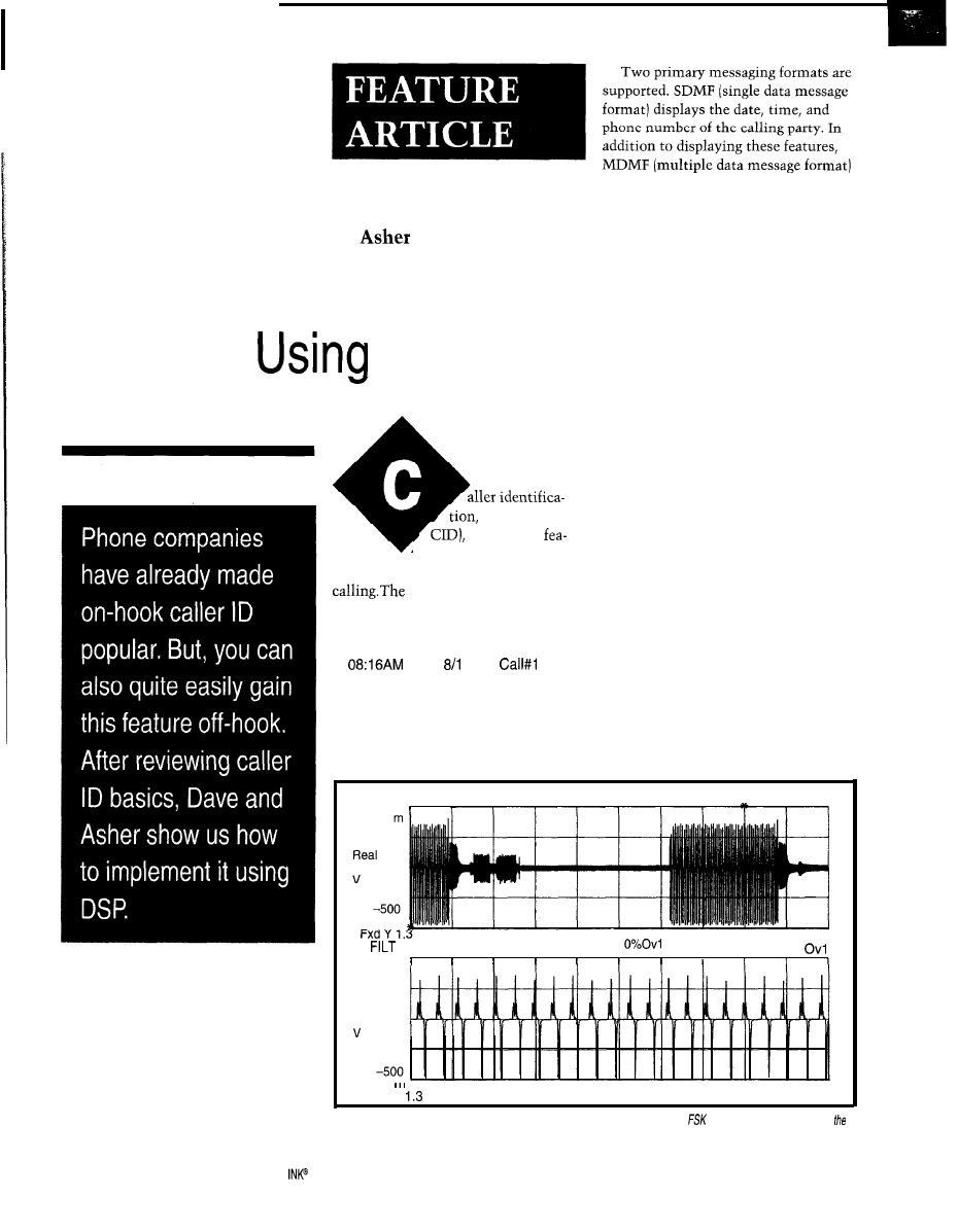
On- and Off-Hook Caller ID Using DSP
Dave Ryan
Hazanchuk
PC Telephone Interface
Chris Sakkas
Embedding the ARM7500
Part 2: Programming an Embedded Computer
Art Sobel
A Winning Proposition
q
Machine Vision
Part 1: Industrial Inspection
Hugh
q
From the Bench
It Can’t Be A Robot
Part 1: There are No Arms and Legs!
Bachiochi
q
Silicon Update
High-Velocity DSP
Tom
Task
Ken Davidson
Life’s Little Mysteries
New Product News
edited by Harv Weiner
Advertiser’s index
Nouveau PC
An In-Depth Look at FTL
Raz Dan
53
Quarter
To ROM or NOT to ROM
That is the Question
Rick Lehrbaum
60
Applied PCs
Right on Cue
National Presents
‘x86
Fred Eady
Circuit Cellar
Issue 83 June 1997
CROSSPOINT DATA SWITCH
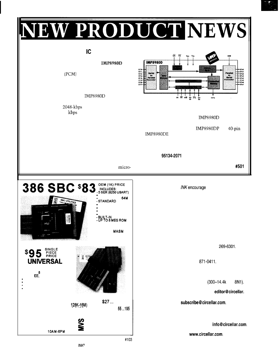
IMP has announced a digital crosspoint switch IC,
accommodating 256 x 256 channels. The
is a
CMOS device that switches digital datastreams such as
pulse code modulated
voice, video, or data signals.
It establishes a path between any input and output over
its internal ST-Bus (Serial Telecom Bus). Uses include
digital exchange, PBX, and central-office applications.
To support 256 channels, the
has eight
each ST-Bus I/O pins. Via time-division multiplexing,
the component-level
ST-Bus supports 32 log-
ical data channels at 64
at each device I/O pin.
ST-Bus bit rate is divided into 8000 frames with 32 chan-
nels per frame.
In the Message mode, the system microcontroller can
pass data onto an output channel. In the nonblocking
Switching mode, the output can specify its input-chan-
nel data source. Multiple outputs can share an input,
which is useful in message-broadcast applications.
A system microprocessor makes switched connec-
tions, writes data to output channels, and can receive
data from input channels. In addition, the system
Edited by Harv Weiner
controller can concurrently read input-channel data and
write data to ST-Bus channel outputs. Large logical-switch
structures are possible since the
can set out-
puts into a high-impedance state on a per-channel basis.
Pricing for the 44-pin PLCC
and
DIP
starts at $7.70 in quantity.
IMP, Inc.
2830 N. First St.
San Jose, CA
(408) 432-9100
l
Fax: (408) 434-0335
www.impweb.com
3 PAR (32 BITS MAX)
32K RAM. EXP
PC BUS
LCD. KBD PORT
BATT. BACK. RTC
IRQO-15 (8259 X2)
0237 DMA 8253 TMR
LED DISP.
-CMOS NVRAM
PROGRAMMER
-DOES
MEG EPROMS
-CMOS,
FLASH, NVRAM
EASIER TO USE THAN MOST
POWERFUL SCRIPT ABILITY
MICROCONT. ADAPTERS
PLCC, MINI-DIP ADAPTERS
-SUPER FAST ALGORITHMS
USE TURBO C,
BASIC,
RUNS DOS AND
WINDOWS
EVAL KIT $295
OTHER PRODUCTS:
8088 SINGLE BOARD COMPUTER . . . . . . . OEM
l
95
PC FLASH/ROM DISKS
. . . . . 75
16 BIT 16 CHAN ADC-DA
. . . . . . . . . . . . . . . . . . 21
C CARD . . . . . . . . . . . . . . . . . . . . .
WATCHDOG (REBOOTS PC ON HANGUP) . . . . . 27 . . . . . 95
l
EVAL KITS INCLUDE MANUAL
BRACKET AND SOFTWARE.
MVS BOX 850
5
YR LIMITED WARRANTY
FREE SHIPPING
HRS: MON-FRI
EST
a
MERRIMACK, NH
.
(508) 792 9507
Contacting Circuit Cellar
We at Circuit Cellar
communication between
our readers and our staff, so we have made every effort to make
contacting us easy. We prefer electronic communications, but
feel free to use any of the following:
Mail: Letters to the Editor may be sent to:
Editor,
Circuit Cellar INK,
4 Park St.,
Vernon, CT 06066.
Phone: Direct all subscription inquiries to (800)
Contact our editorial offices at (860) 875-2199.
Fax: All faxes may be sent to (860)
BBS: All of our editors and regular authors frequent the Circuit
Cellar BBS and are available to answer questions. Call
(860) 871-1988 with your modem
bps,
Internet: Letters to the editor may be sent to
corn. Send new subscription orders, renewals, and ad-
dress changes to
Be sure to
include your complete mailing address and return E-mail
address in all correspondence. Author E-mail addresses
(when available) may be found at the end of each article.
For more information. send E-mail to
WWW: Point your browser to
6
Issue
93 June 1997
Circuit Cellar
LOW COST KIT
A low-cost I/O
kit,
IO/U,
is available from Take Con-
trol. The double-sided PC board supports 64 analog in-
puts, 64 digital inputs, and 64 digital outputs. As well, it
supports a DTMF decoder and generator, IR amplifier,
watchdog timer, power supplies, and a high-speed paral-
lel interface that plugs into a bidirectional PC printer
port.
Applications include robotics, home automation,
weather logging, data acquisition, operator interface,
ham repeater/remote base controller, and antenna tracker.
The board features a
ADC (Maxim’s MAX180).
Its open collector digital-output relay drivers can sink
150
and all TTL-level digital inputs include pull-up
resistors. The unit’s modular design enables the user to
build just the needed sections. All analog and digital I/O
uses 34-pin IDC cables.
Prices start at $79 for the bare board, instruction man-
ual, and software (Turbo C source-code and BASIC
driver examples). A complete kit, including all parts and
a wall transformer, is available. Cables, enclosure, ship-
ping, and sales tax are not included.
Take Control, Inc.
280 Church St.
l
Clayton, GA 30525-1473
(706) 782-9848
l
Fax: (706) 782-2277
www.takecontrol.com
Touch The Future
LCD Touch Monitors
L C D T o u c h S c r e e n s
V G A L C D D i s p l a y s
LCD Controllers
ISA,
Analog, Video
EARTH
Lowest Prices on Earth!
Computer Technologies
27101 Aliso Creek Rd
154 Aliso
CA 92656
Ph: 714-448-9368 Fax: 714-448-9316
FREE CATALOG available at
l
Choose from over 700
module footprints with
surface
mounts, or create
vour own desions
No.
Price
137605
PCB CAD
137592
CAD 224.95
Interface Board Kit
More
kits
available!
l
Pass through paral-
lel connection
l
16
with opto coupler
l
Analog outputs: (8)
(64 steps),
(256
l
Analog Inputs: (4j
(256 steps)
Parr No. Description
Price
Programming speeds/
algorithms: normal,
and quick pulse
No. Description
101400
programmer .
FAX:
(Domestic)
FAX:
(International)
Ordering Hours:
E-mail:
Basic
Stamp@ Rev. Kit
Additional Parallax
available!
Description
Price
140089 Basic Stamp kit $79.95
8031
Embedded
Applications
PC Board
No. Description
Price
119546
PC board $99.95
L o w
Cost Board
l
16
S.E. analog inputs
with
resolution
No. Product No.
Price
Programmer
l
Programs 16Kbits
to 512Kbits
8
Issue 83 June 1997
Circuit Cellar INK@
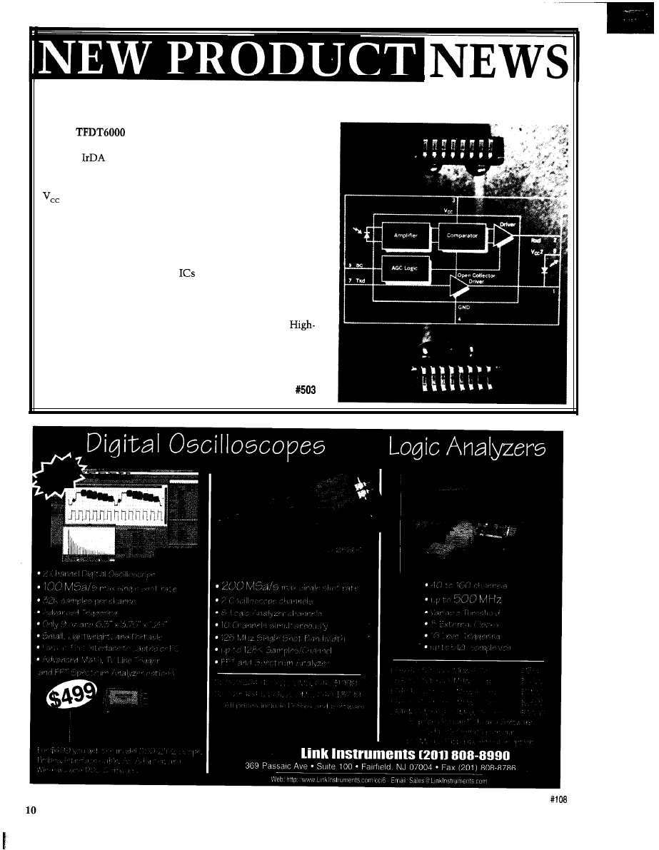
INFRARED TRANSCEIVER
The
is a multimode integrated IR transceiver
module for data-communication systems. The transceiver sup-
ports all
speeds up to 4 Mbps, HP-SIR, and Sharp ASK
modes. Integrated into this tiny package are a photodiode, IR
LED, and analog IC. A current-limiting resistor in series and a
bypass capacitor are the only external components required
to implement a complete transceiver.
The transceiver uses a complete differential design for supe-
rior interference rejection. It features 5-V operation and low
power consumption. By integrating the receiver’s preamplifier
and the transmitter’s driver stage, the TFDT6000 transceiver
combines the functions of two
and eliminates a large num-
ber of external components. A typical discrete implementation
requires up to nine separate components.
The transceiver is offered in a surface-mount epoxy resin
package measuring 0.52” x 0.30” with a height of 0.23”.
volume pricing is $4.50 each.
Temic Semiconductors
2201 Laurelwood Rd.
l
Santa Clara, CA 95054-l 595
(408) 567-8220
l
Fax: (408) 567-8995
Issue 93 June 1997
Circuit Cellar INK@
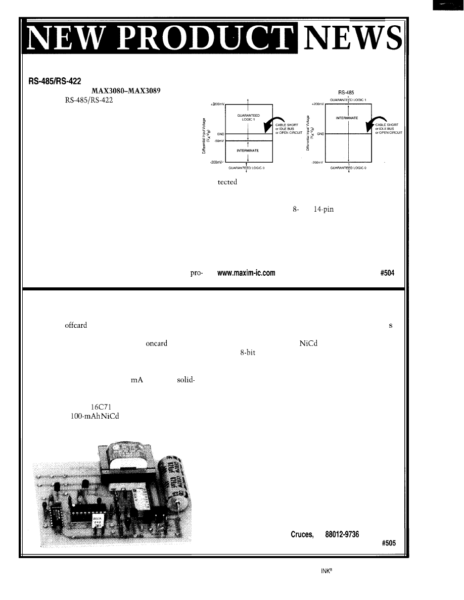
TRANSCEIVERS
FAIL-SAFE OUTPUT GUARANTEES LOGIC 1 DURING SHORT OR OPEN CIRCUIT
Each item in the
family of
THE MAXIM WAY
OTHER
DEVICES
high-speed
communications trans-
ceivers includes one driver and one receiver. The
devices feature fail-safe circuitry, guaranteeing a
logic-high receiver output when the receiver inputs
are open or shorted. Thus, the receiver output is a
logic-high if all transmitters on a terminated bus are
disabled (high impedance).
The MAX3080, ‘8 1, and ‘82 feature reduced slew-
rate drivers that minimize EM1 and reflections caused
by improperly terminated cables, enabling error-free
data-transmission rates up to 115 kbps. The MAX3083,
‘84, and ‘85 offer higher driver output slew-rate limits,
allowing transmit speeds up to 500 kbps. The MAX3086,
‘87, and ‘88 driver slew rates are unlimited, so transmit
speeds up to 10 Mbps are possible. The MAX3089 slew
rate can be 115 kbps, 500 kbps, or 10 Mbps by driving a
selector pin with a single tristate driver.
All devices have a ‘/R-unit-load receiver input imped-
ance that enables up to 256 transceivers on the bus.
Driver outputs are short-circuit-current limited and
by thermal shutdown circuitry that puts them in a
high-impedance state to avoid excessive power dissipa-
tion.
The devices come in and
plastic DIP and SO
packages. Prices start at $1.25 in quantity.
Maxim Integrated Products
120 San Gabriel Dr.
Sunnyvale, CA 94086
(408) 737-7600
l
Fax: (408) 737-7194
OVER/UNDER VOLTAGE PROTECTOR
The “Smart” Protector Type 6 (SPPC-6) PC board
controls an
solid-state relay to disconnect a load
if the AC power-line voltage exceeds programmed limits.
The nominal line voltage is set via an
DIP switch.
High and low voltage limits are proportional to the pro-
grammed voltage (i.e., 110-140 V when set for 125-V
operation, and 95-125 V with a 110-V line). Power avail-
able for the controlled relay is 6
max., so a
state relay must be used. Load current depends on the
relay rating.
A Microchip PIC
microprocessor, powered by a
rechargeable
battery, monitors the AC
power-line voltage. If the voltage exceeds limits, the
relay opens and the load disconnects. The circuit auto-
matically resets itself and reconnects the load after 80
when the line voltage returns within limits. An on-card
circuit trickle charges the
battery.
The
ADC output (proportional to monitored
voltage) is broadcast as a serial RS-232 signal to enable
display and logging. A two-wire interface is used, and
handshaking with the receiver is not needed. Sample
MS-DOS software is supplied.
The user can select the Protector response during a
power outage. If a DIP switch is off, the microprocessor
enters sleep mode to conserve battery power, but it con-
tinues to monitor the AC line. When the switch is on,
the microprocessor continues to broadcast the voltage (0,
in this case) over the RS-232 line. This feature is useful
when outage and restore times need to be logged but
battery current is -30% higher. When power returns,
reset is automatic.
A built-in test circuit simulates an out-of-limits line
voltage with a single-pole, normally open push-button
switch.
The SPPC-6 sells for $42.
TDL Electronics
5260 Cochise Trail
l
Las
NM
(505) 382-8175
l
Fax: (505) 382-8810
Circuit Cellar
Issue 83 June 1997
11
FEATURES
DSP-Based Canadian
Receiver
On- and Off-Hook Caller
ID Using DSP
PC Telephone Interface
Embedding the
ARM7500
Receiver
David Tweed
Part 1: Identifying
Techniques
lot has been writ-
ten recently about
digital signal processing,
especially since the advent
of low-cost general-purpose DSP chips
like the Texas Instruments TMS320
series, the Motorola DSP56000, and
the Analog Devices ADSP-2101 family.
Digital filtering and spectral analysis
have been covered as well as high-level
application topics such as speech,
music, image, and video compression.
But, with the nuts and bolts of finite
impulse response (FIR) versus infinite
impulse response (IIR) filters, or corre-
lation functions, or discrete Fourier
transform (DFT) versus fast Fourier
transform
many people get lost
in the details and mathematics.
In this two-part series, I want you to
gain a more intuitive feel for these
topics. So, I skip (most of] the math,
and concepts are presented graphically.
I also discuss the practical tradeoffs
associated with using these techniques
in a real application.
Part 1 introduces the application and
walks through the high-level design to
identify the necessary DSP techniques.
I examine two techniques-cross-corre-
lation and FIR filtering-in detail.
In Part 2, I discuss the Fourier Trans-
form and real-world issues that arise
12
Issue
93 June 1997
Circuit Cellar INK@
Voice
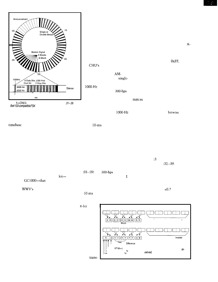
:oo
until
beginning of
I
0
100
next
200
300
400
second
500
Figure
signal repeats each minute. Seconds
contain
a
modem signal between the second ticks.
time signal can be
found on 3.330, 7.335, and
14.670 MHz. It’s an
compatible full-carrier
sideband signal, containing
beeps, voice an-
nouncements, and a
modem signal. Figure
1 shows
how the components fit
together.
As you can see, the heavy
when signals don’t resemble textbook
examples. To wrap up, I show how to
use direct digital synthesis to create a
independent of the CPU clock.
THE APPLICATION
It’s fairly well-known that station
lines of the figure represent the
tone. It comes in 500 ms at the top of
the minute, 300 ms or double tones as
indicated, and
ticks when a
voice announcement or modem signal
is needed.
WWV in Boulder, Colorado (and WWVH
in Hawaii) broadcasts time signals that
can be received over most of North
America. These signals contain compo-
nents that can be decoded with rela-
tively simple hardware to keep a clock
synchronized to the international
Universal Coordinated Time (UTC).
Figure 2 shows the two types of
blocks as received by a CPU. Once the
data is in memory and the redundancy
bytes checked, swap the least and most
significant nibbles in each byte.
In the A block, the 6 is a constant,
DDD is the day of the year, and hh:
is the UTC time of day (at the
beginning of the current second). Each
nibble is a BCD digit.
In the B block, X is a
field,
and D is the absolute value of DUT in
tenths of a second. YYYY is the Grego-
rian year, and TT is the difference
between TAI and UTC.
The A nibble flags Canadian Day-
light Time (this nibble’s contents are
currently undocumented). The B nibble
is a serial number that increments
when the B-block format changes.
A B block transmits once per min-
ute, at second 1. An A block trans-
mits during seconds
DUT is a signed number represent-
ing the difference between UTC (atomic
time) and UT1 (astronomical time). It
varies in a complex way because of
slight variations in the earth’s rotation
rate. When it reaches
s, a leap
second is added to or deleted from UTC,
2225 Hz, representing a binary 1 or idle
usually at the next new year.
state. It’s followed
by
ten
bytes
The announcement alternates be-
tween the station ID and time in En-
glish followed by the time in French
(on even minutes) and the station ID
and time in French followed by the
time in English (on odd minutes).
For some years, Heath offered a
the Model
took advan-
tage of this. Unfortunately, in New
England,
signals are weak and
fading at best. Plus, they’re often non-
existent for large segments of the day.
At the top of each hour, the :00 tone
is extra long, and there is no tone for
seconds
The
modem
signal shown at the bottom of Figure
is Bell 103 compatible, using 2225 Hz
for mark and 2025 Hz for space.
Each data burst begins immediately
after the
tick with 123.3 ms of
It’s less well-known that Ottawa,
Canada’s CHU broadcasts a similar
time signal that covers New England
fairly well. It also can be decoded to
automatically set a clock.
This signal’s structure is quite dif-
ferent from those of WWV and WWVH.
So, other techniques are necessary to
extract the relevant information.
I designed a software-based CHU
time-signal decoder that runs on a
common DSP development board. It
uses an ordinary shortwave receiver’s
audio output and produces an RS-232
ASCII output to set and/or
display the time.
While this application is a
little contrived, it’s a good
base for discussing DSP. And,
it demonstrates how far we
can push the performance
envelope in terms of accuracy
and tolerance to noise and
fading.
CHU SIGNAL
mit. The last stop bit ends exactly
500 ms into the second and is followed
by another 10 ms of 2225 Hz to avoid
false overrun of the stop bits. The
remainder of each second is silent.
Each data block contains 5 bytes of
data (divided into ten 4-bit nibbles),
followed by 5 redundancy bytes. The
format redundancy bytes are exactly
like the data bytes. The B-format redun-
dancy bytes are exactly inverted
(l’s
complement, NOT, XOR
etc.)
from the data bytes.
of data, each
framed with a
start bit of 0 and
two stop bits of 1.
With either of
the two types of
data blocks (A or
B), the data with
its start and stop
bits requires 110
bit times (i.e.,
366.7 ms) to
A Block Format
Redundancy Bytes Same as Data
Day of Year
Minutes Seconds
B Block Format
Redundancy Bytes are Data
TAI
UT1 Difference
Sign of
Leap-Second Warning: will be added
Leap-Second Warning: will be deleted
Even Parity for this Nibble
Figure 2-Once the data bytes are
the nibbles must be swapped to
make sense of them.
Circuit Cellar INK@
Issue 83 June 1997
13
In
55.0
55.1
55.2
55.3
55.4
55.5
55.6
55.7
55.8
55.9
56.0
56.1
56.2
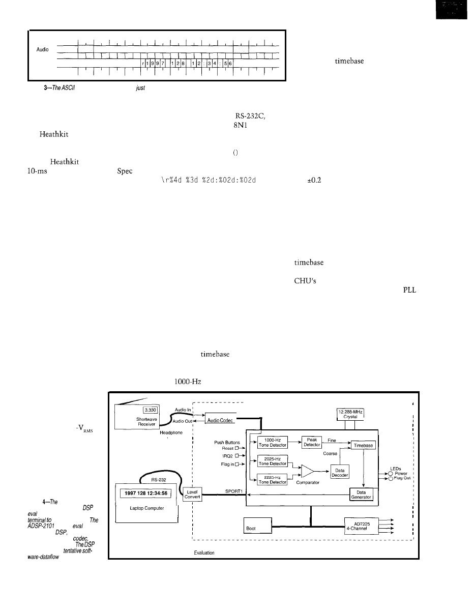
ASCII Out
Figure
output of the receiver ends
as the corresponding second begins.
A BETTER MOUSETRAP
RS-232 OUTPUT
Suppose you want to build a clock
that sets itself to the CHU signal like
the
clock does to the WWV
signal. And, you want to see how pre-
cise you can get this signal.
The
clock guarantees
accuracy when its Hi
light
is on, but I think submillisecond accu-
racy is possible.
I
want a lot of infor-
mation out of the audio signal despite
its noisiness.
Under most conditions, CHU offers
a stronger signal than WWV to New
England. However, it’s still subject to
severe fading.
The clock should provide continuous
output regardless of the radio signal’s
condition, while keeping the best pos-
sible accuracy. That’s why I didn’t just
use a $15 modem.
FUNCTIONAL SPECIFICATION
I wanted to generate an RS-232 out-
put that gives the time of day as an
ASCII string every second, based on
the signal received from CHU.
This string has a fixed length of
18 bytes and is transmitted so the last
byte ends at the time represented by
the string (see Figure 3). The screen
appears in sync with the audio, but I
started transmitting the string 18 char-
acter times before the represented time.
ACCURACY
Since the signal isn’t always avail-
The local
should be as
able, the product needs a local timebase.
accurate as possible within the limits
I wanted to avoid RF, so I used the
imposed by the radio link and receiver.
audio output of a shortwave receiver.
The
tones give a basic 1-pps
The audio input is
from the headphone
jack of a general-cover-
age shortwave receiver,
which gives a 1
signal. The DSP evalu-
ation board’s audio
input should accept
this directly.
TP3054
Jack
ADSP-2101
SPORT0
Integer DSP
Figure
complete
time
receiver has a radio, fhe
board, and a computer or
display the time.
EZ-Lab
board
includes the
a boot PROM,
a voice-grade audio
and
a
four-channel DAC.
outline
offers a
diagram.
The output signal is
using
ASCII characters in an
configura-
tion. The data rate would range be-
tween 300 and 9600 bps.
Using C pr i n t f
notation, the
output string is:
where the individual fields are year,
day, hours, minutes, and seconds UTC
(using 24-h notation). \ r represents a
bare CR.
When observed on a screen or emula-
tor, the time display updates in place
onscreen, leaving the cursor at the end
of the string between updates.
(pulse per second) indication. Depend-
ing on how accurately I identify the
tones’ start and stop transitions,
I
can
set the local
to within a few
milliseconds.
By discriminating individual cycles
of the 1000 Hz, I can get it to around
1 ms. And, if I can accurately measure
the tone’s relative phase angle, I might
get O.l-ms or less error.
However, the radio-path length
between Ottawa and eastern Massachu-
setts is -700 km. And, it can vary by
-10% as the ionosphere varies in height
and reflectivity.
At 300,000 km/s, the path delay is
-2.2
ms. So, the accuracy goal
should be -1 .O-ms maximum instanta-
neous error.
TOP-DOWN DESIGN
Once the product’s task is set, con-
sider which technologies to use.
I need to decode audio tones at 1000,
2025, and 2225 Hz. I also need a local
to generate ASCII output
messages which synchronizes with
signal when it is available.
While analog filters along with
(phase-locked loop) circuits handle tone
decoding and the local timebase, they
are rather inflexible for trying different
algorithms or if the functional require-
ments change. Also, getting everything
to work together optimally is a com-
plex calibration process.
To demonstrate DSP techniques
with an off-the-shelf evaluation board,
I
chose an all-software implementation.
27512
PROM
Memory Bus
I
DAC
Debug
ADSP-2101
Board
14
Issue 83
June 1997
Circuit Cellar INK@
16
SOLID STATE
DRIVE
4M Total, Either Drive Bootable
Card 2 Disk Emulator
Flash System Software Included
FLASH SRAM Customs too
486
SINGLE CARD
COMPUTER
Up to
drive
Compact-XT height card size
Industry Standard PC-l 04 port
L2 cache to
to
Dual IDE/Floppy connectors
All Tempustech
products are
PC Bus Compatible. Made in the
U.S.A., Day Money Back Guarantee
1, Qty breaks start at 5 pieces.
TEMPUSTECH, INC.
TEL: (800) 634-0701
FAX: (941) 643-4981
E-Mail:
I-Net:
Fax for
fast response!
295 Airport Road
Naples, FL 34104
Issue 83 June 1997
Circuit Cellar
Figure 4 shows the complete hard-
ware of the time receiver. It comprises
a Realistic DX-380 receiver, Analog
Devices’ EZ-Lab board for the
2101, and a TRS-80 Model 100 laptop.
Within the dotted line is the block
diagram of the DSP evaluation board.
It includes an audio
for the A/D
conversion. An RS-232 level converter
on serial port 1
generates the
correct voltages for the output signal.
The four-channel DAC connects to
an oscilloscope for algorithm develop-
ment and debugging. There, it graphi-
cally indicates the
real-time
activity.
The software takes in 8000 audio
samples per second-more than suffi-
cient to handle the bandwidth. It gen-
erates ASCII output messages as well.
In between, it detects tones and
decodes CHU signal’s data. Using this
information, it establishes a local
base relative to the CPU’s crystal. The
then drives the output-mes-
sage generator.
Figure 4 illustrates the required
components and how they interact. I
fully develop this diagram after dis-
cussing possible techniques for tone
detection and establishing a timebase.
TONE DETECTION
receiver’s operation. Because I want
From this diagram, you see that
tone detection plays a major role in the
high accuracy, it’s important to deter-
mine the existence or nonexistence of
tones and to find when they begin and
end-down to a single cycle or less.
Many people believe this is what
are for. But, the FFT is most
useful when you’re looking for one or
more tones but don’t know their fre-
quency. It’s overkill when looking for
a tone at a particular frequency, and it
isn’t particularly good at locating a
tone’s start and stop edges.
A Fourier Transform (FT) converts a
block of numbers representing signal
samples in time into the signal’s fre-
quency components for that period. It
can’t tell you whether a given compo-
nent was there for the whole block of
time or only part of it.
The best you can do is see whether
the component is present in one block
but not another. This limits time reso-
lution to the FFT’s block size.
So, you use small sample blocks to
get good resolution. But, there’s a
tradeoff. The number of frequency bins
at the FFT’s output is proportional to
the number of time samples at the
input.
For a given sample rate, each bin’s
size grows as the number of bins goes
down, so it’s harder to discriminate
among frequencies that are close to-
gether. Thus, you need large sample
blocks to get good frequency resolution.
helps locate signals in time.
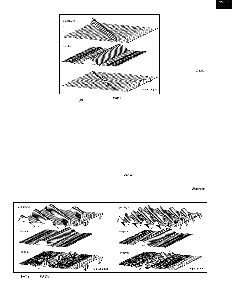
CROSS-CORRELATION
Suppose you have two signals. One
is a template for a simple
tone
Obviously, you can’t have good
time and frequency resolutions simul-
taneously with an ordinary FFT. A
different
Figure
graphs show
of an incoming
(doffed
with a template
The
dashed line shows point-by-point multiplication of
functions.
line over
yields a single
in overall cross-correlation
b-This graph includes markers for
four
alignments.
Sine Template
Sum of
Sum of
Figure
cross-correlation
can be represented as a
dimensional structure. Redoing the process using a cosine template enables
the
of
phase-angle information.
burst. Does the other signal contain
this tone burst?
The signals are both functions of
time. So, line the template up with the
unknown signal at various offsets in
time to see how they match up.
Figure 5a shows several such trials.
The solid line represents the template
function. The incoming signal is shown
as a dotted line at various offsets (At).
The matching is done via a
relation between the
signals, and if the result
is positive, there is
positive correlation.
By making many
trials at various values
of At and generating a
correlation value for
each, I can graph these
values as a function of
At. Figure 5b has verti-
cal markers showing
values for the trial align-
ments. The fourth trial
in Figure 5a shows
perfect alignment at a
At value of 0, corre-
sponding to the highest
peak in Figure
Figure 6 shows this
process differently.
Here, (time) varies left
to right, and At from
front to back. The top
section gives the input
signal, shifting left to
right as At varies.
The second section shows the tem-
plate function, which doesn’t change
with At. The middle section represents
the point-by-point multiplication of
the first two sections. Each layer is a
different trial alignment of the input
signal with the template.
Integrating the middle section left
to right (i.e., over time) gives a single
value for each trial, representing the
value of the cross-correlation. Together,
by-point multiplication of the two
these points represent the
function values. See the result in the
lation function of At.
dashed line.
In effect, this integration “projects”
Note, when either function is zero,
the surface onto the two-dimensional
the result is zero. If both functions are
graph shown running front to back at
positive or both are negative, the
result is positive. If the signs are
opposite, the result is negative.
I boil this down to a single
number for each trial by adding
up (integrating) the individual
multiplication results. If the re-
sult is zero or near zero, the sig-
nals are uncorrelated. If the result
is negative, there is negative
Figure
‘I-Combining results from sine
and cosine analyses allows phase angle
difference be calculated at each
Data Acquisition
new Value-Line has
uncompromising design features
and high quality components at
prices below the low cost guys!
Just check out the specs:
5500MF
8 channels
A/D,
16 digital I/O, Counter/Timer
H i g h S p e e d
8 channels
DMA
M u l t i - F u n c t i o n D M A
5516DMA
16 channels
A/D,
DMA, 16 digital
R e s o l u t i o n
16 channels
A/D,
DMA, 8 digital
learn more:
voice
800-648-6589
fax
617-938-6553
web
www.adac.com
American Data Acquisition Corporation
70 Tower Office Park,
MA 01801 USA
Circuit Cellar
Issue 83 June 1997
17
the right. A single trial
alignment is represented as
a slice parallel to the paper
surface, and it represents a
single value on the final
graph.
DISCRETE TIME
I’ve been cheating a bit.
In these graphs, I pretended
the template and input
functions are continuous
with respect to time. Actu-
ally, they’re sequences of
numbers representing
samples of the continuous
functions.
Product
Figure 8-An input signal consisting of a single
sample
simple reads out the
template function
coefficients) in sequence.
template and input functions. The best
I can do is generate one cross-correla-
tion value for each input sample pro-
cessed.
Therefore, I can’t arbi-
trarily make many trial
alignments between the
I have a second, related problem.
Since the clock taking samples isn’t
synchronized to the clock generating
the signal at the transmitter, I can’t
count on a sample occurring at the
peak of the cross-correlation function.
However, I can compensate for
these issues. Consider what happens if
I take a second cross-correlation using
a cosine wave as the template, which
is another way of describing a sine
wave shifted by 90” (a quarter of a
near the centers of both analyses and
plot the result of the sine correlation
The resulting points lie on a circle.
against the result of the cosine correla-
If I draw a line from each point to the
circle’s center, its angle relative to the
x-axis represents the phase angle of the
tion (see Figure 7).
input signal with respect to the cosine
template.
I get a numerical value for this
phase angle by taking the arctangent of
the ratio of the two results. This value
can have any resolution and may rep-
resent fractions of the sample period.
So, if the true peak of the
at the next calculation. It’s
easy to do a linear interpo-
lation between these two
angles to calculate the
exact moment the phase
angle went through 0.
FIR FILTER
Now for something
completely different. The
Finite Impulse Response
(FIR) filter is an algorithm
commonly used on
because of its predictable
characteristics and nice,
regular structure.
Treated as a black box,
it takes in a sequence of
numbers representing a
signal’s samples and out-
puts a new sequence of numbers repre-
senting the filtered version of the
input signal.
Internally, the FIR filter is imple-
mented as a series of registers that
hold the input sample and copies of
previous input samples. As each sample
arrives, the oldest sample is discarded.
The whole set of samples is multi-
plied by a set of numbers (the filter’s
coefficients), the products are summed,
and this sum becomes the current
output sample. This process repeats at
the sample rate.
The filter’s coefficients are the same
as its impulse response. Consider what
wavelength).
The bottom sections of Figure 6
show the same analysis with a cosine
template. I can take the results from
correlation function falls between two
happens if all the registers contain 0
actual samples, I get a negative phase
and a sample of I arrives, followed by
angle as part of the answer for the first
more 0 samples, which is the
calculation but a positive phase angle
time version of an impulse function.
Figure
low-pass
has a large output for a signal below its cutoff frequency but a tiny output for a signal above it.
18
Issue 83 June 1997
Circuit Cellar INK@
As the 1 propagates through the
registers, it is multiplied once by each
coefficient in sequence. All other coef-
ficients are multiplied by 0. The se-
quence of output samples, representing
the filter’s response to the impulse
stimulus, matches the sequence of
coefficients exactly.
As Figure 8 shows, the only differ-
ence between the FIR filter and
correlation function is terminology.
“Template function” is now “impulse
response” or “filter coefficients.” And,
what I called “At” is now the registers
holding the older input samples.
In effect, the output of the FIR filter
is a signal that, from moment to mo-
ment, tells how well the input sample
matches or correlates with the impulse
response. Therefore, you’ll sometimes
see the term “matched filter” used in
certain signal-processing applications.
The coefficients in Figure 8 imple-
ment a low-pass filter. Figure 9 shows
what’s going on within the filter for
signals both below and above the cut-
off frequency.
For the signal above the cutoff fre-
quency, the outcome of the multiplica-
tion step has nearly equal amounts of
positive and negative results, giving
almost total cancellation and a very
small output signal.
It isn’t obvious why this set of coef-
ficients implements a low-pass filter.
The math shows that the frequency
response is the FT of the impulse re-
sponse.
UPCOMING
In Part 2, I return to the FT and look
at building a local copy of the UTC
timebase. I also cover the details of
implementing the algorithms discussed.
One set of software tone detectors
demodulates the FSK data to coarsely
set the timebase, and another
tunes the setting based on a
burst.
David Tweed has been developing
real-time software for microprocessors
for more than 18 years, starting with
the 8008 in 1976. He currently designs
equipment to carry high-quality audio
and wide-bandwidth data over digital
telephone services such as and
ISDN. You may reach him at dave.
graphics for this article
are on the Circuit Cellar Web site.
Radio station CHU,
inms/whatime.html.
Radio station
www.
boulder.nist.gov/timefreq.
D.L. Mills, Gadget Box
Level
Converter and CHU Modem,
www.
ntpdoc/gadget.html.
Inc.
101 Main St.
Cambridge, MA 02142-1521
(617)
Fax: (617) 577-8829
www.mathsoft.com
TRS-80 Model 100
Andy Diller’s Web 100 Main Page
ADSP-2181, EZ-Lab,
EZ-Lab Lite
Analog Devices
One Technology Way
MA 02062-9 106
(617) 329-4700
Fax: (617) 329-1241
www.analog.com
DSP56000
Motorola
MS OE314
6501 William Cannon Dr. W
Austin, TX 78735-8598
(512) 891-2030
Fax: (512) 891-3877
TMS320 series
Texas Instruments, Inc.
34 Forest St., MS
Attleboro, MA 02703
(508) 699-5269
Fax: (508) 699-5200
www.ti.com
401
Very Useful
402 Moderately Useful
403 Not Useful
Add these numbers up:
a ‘51 Compatible Micro
40 Bits of Digital
8 Channels of 10 Bit A/D
3 Serial Ports
or
2 Pulse Width Modulation Outputs
6 Capture/Compare Inputs
1 Real Time Clock
64K bytes Static RAM
+ UVPROM Socket
5 12 bytes of Serial EEPROM
1 Watchdog
1 Power Fail Interrupt
1 On-Board Power Regulation
It adds up to real
That’s
our
popular
OEM
priced at just $299 in
single quantities. Not enough I/O?
There is an expansion bus, too!
Too much I/O? We’ll create a
version just for your needs, and
pass the savings on to you!
Development is easy, using our
Development
Board:
The
Development board
with ROM Monitor for $349.
Our popular 803 1 SBC can now be
shipped with your favorite 8051
family processor. Models include
1 FA,
a n d
more. Call for pricing today!
The
Plus is a low-cost
alternative to conventional ICE
products.
Load, single step,
interrogate, disasm, execute to
breakpoint. Total price for the
base unit with most pods is a low
$448. Call for brochure, or World
Wide Web at www.hte.com.
S i n c e 1 9 8 3
(619) 566-l
Internet e-mail:
World Wide Web: www.hte.com
Circuit Cellar INK@
Issue 83 June 1997
1 9
Dave Ryan
&
Hazanchuk
gives the caller’s name as it appears in
the telephone book. This information
arrives via two methods of delivery-
on- or off-hook.
On- and Off-Hook
Caller ID
DSP
(caller ID or
is an added
ture of the telephone sys-
tem that visually indicates who is
display, usually a custom
LCD with 2-4 lines of information,
might look like:
8
408-370-8504
Dave Ryan
can therefore be filtered out.
Before picking up the phone, you
can identify the caller. Unwanted calls
On-hook delivery transmits infor-
mation between the first and second
rings of the incoming call. This method
is widely implemented in analog sys-
tems and is commercially available.
Off-hook delivery, is also called
SCWID [spontaneous call waiting with
caller ID) or CIDCW (caller ID with
call waiting). When a third party tries
to connect with two parties already
engaged with each other, information
is only transmitted if an acknowledg-
ment is received from the party to be
interrupted. This method is not com-
mercially available.
In addition to the various call-wait-
ing signals transmitted from the SPCS
(stored program control system], a spe-
cial CAS (customer premises equip-
ment alerting signal) is also sent. The
basic data is transmitted using FSK
(continuous phase binary frequency
shift keying).
ON-HOOK DELIVERY
current, demodulate the FSK signal,
This fairly simple system only
requires circuitry to-detect the ringing
CAP TIM BUF
500
TIME 1
p
9.3
500
m
Real
Fxd Y
2.1
Figure l--The high-amplitude, low-frequency signal is the ringing voltage.
The
data-transmission signal
is
short burst of low-amplitude, high-frequency signal that
appears between the first and second rings.
20
Issue 83 June 1997
Circuit Cellar
5 0 0
1000 1 5 0 0 2 0 0 0 2 5 0 0 3 0 0 0 3 5 0 0
Example data shown above is 1010
-2.50000 ms
0.00000
2.50000
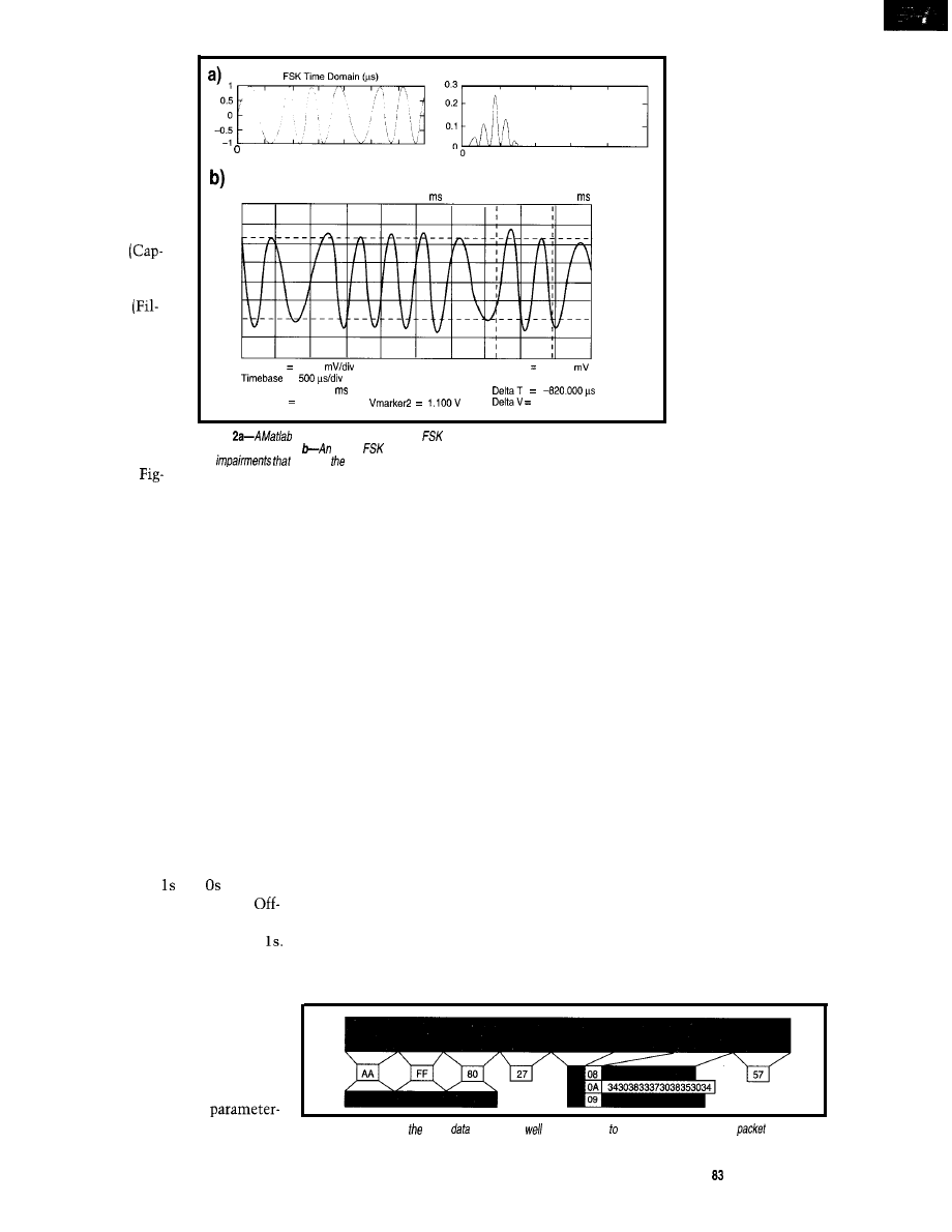
ure 2a. The data alternates between 1,
and display the result-
ing data.
0,1, and 0. The power spectral density
Figure 1 shows the
delivery of FSK data
plot shows this signal’s frequency
sandwiched between
the first and second
content in the frequency domain.
rings. The larger am-
plitude, lower frequen-
cy waveforms at the
beginning and end of
CAP TIM BUF
tured Time Buffer) are
the ringing pulses.
FILT TIME 1
tered Time 1) shows
the ringing pulses in
greater detail. The
smaller amplitude,
higher frequency wave-
form is the FSK data.
A somewhat ideal-
ized simulation of the
data is shown in
Cl. 1
5 0 0 . 1
offset
- 4 0 . 0 0
=
Delay
= 0.00000 s
start
= 1.99000
stop
1.15000 ms
V m a r k e r l -1.000 V
2 . 1 0 0 V
Figure
simulation shows idealized
and ifs corresponding power spectral density in
the frequency domain.
actual
transmission caught using a storage scope shows some of
the
occur in real world (e.g., over- and undershoots).
2 0 0 0 4 0 0 0
6 0 0 0
6 0 0 0
1 0 0 0 0
Power Spectral Density (Hz)
Of course, real-world data is never
as clean idealized situation. Figure 2b
shows actual received data.
It’s easy to see that the amplitudes
of the high and low-frequency segments
are quite different. In addition, noise is
superimposed on the signal, most
noticeably on the peaks and troughs.
SDMF AND MDMF
Although SDMF displays only the
date, time, and phone number, MDMF
give the caller’s name as well. In fact,
via MDMF, any ASCII data may be
transmitted.
Figure 3 shows a simplified overview
of the MDMF. The channel seizure is a
series of alternating and that are
only supplied in the on-hook case.
hook as, data transmission starts with
the mark signal, which is a series of
Parameter words are not limited to
one message. There may be many
parameter messages, each consisting of
a parameter type, length, and word.
Just to complicate matters, optional
mark signals may be sent between
frames. At the end of every transmis-
sion is a checksum we describe in
detail later. Notice that the
data length can vary.
Figure 4 illustrates an on-hook
solution. An FSK band-pass filter filters
The SDMF/MDMF section removes
the start and stop bits and determines
signals, and the FSK demodulator con-
the messaging format. Data is stored in
verts the analog signal into binary data.
SRAM or displayed on the LCD.
LCD
The display is usually a small LCD
capable of showing the caller’s date,
time, telephone number, and name. It
usually has enough memory to store
30-99 calls.
The system is usually battery pow-
ered since the time of system opera-
tion is generally limited to the time
between the first and second ring. Once
the call is answered, the system may
be put in power-down or standby mode.
WHY DSP?
Digital signal processing isn’t nec-
essary for on-hook operation. Relatively
simple and cost-contained analog solu-
tions exist. DSP makes much more
sense for off-hook
operation.
The difficulty arises
in accurately detect-
ing the special CAS
tone in the presence
of VOX. The chip
must avoid inadvert-
ent detection due to
the similarity with
speech (the Talk Off
problem).
This type of system
hasn’t been widely
implemented in ana-
log solutions prima-
rily because implem-
enting a cost-contain-
ed, manufacturable,
and robust solution is
difficult.
With digital filters,
the manufacturing
difficulties associated with using criti-
cally matched components [e.g., resis-
tors, capacitors, inductors, etc.) are
largely avoided. In addition, the solu-
tion may now be made adaptive.
Variant, implementations then be-
come simply a matter of software up-
grades. Of course, there are tradeoffs.
A/D conversion must be supported
with its ancillary requirements, and so
must D/A conversion. However, usu-
ally, a DSP solution seems far superior.
BUILDING A CALLER-ID SYSTEM
The simplest way to get caller ID is
to purchase a ready-made evaluation
board complete with firmware. How-
ever, it’s certainly possible to write the
software and build the hardware.
While building the hardware is
reasonably straightforward, software
development is a little more complex.
You’ll definitely need some firmware
development tools (e.g., an emulator,
assembler, linker, and debugger).
You can see the system in Figures 5
and 6. The system blocks for it are:
Figure 3-Here, you see digital
overview as
as
ifs relation fhe overall messaging or
structure.
Circuit Cellar INK@
Issue June 1997
21
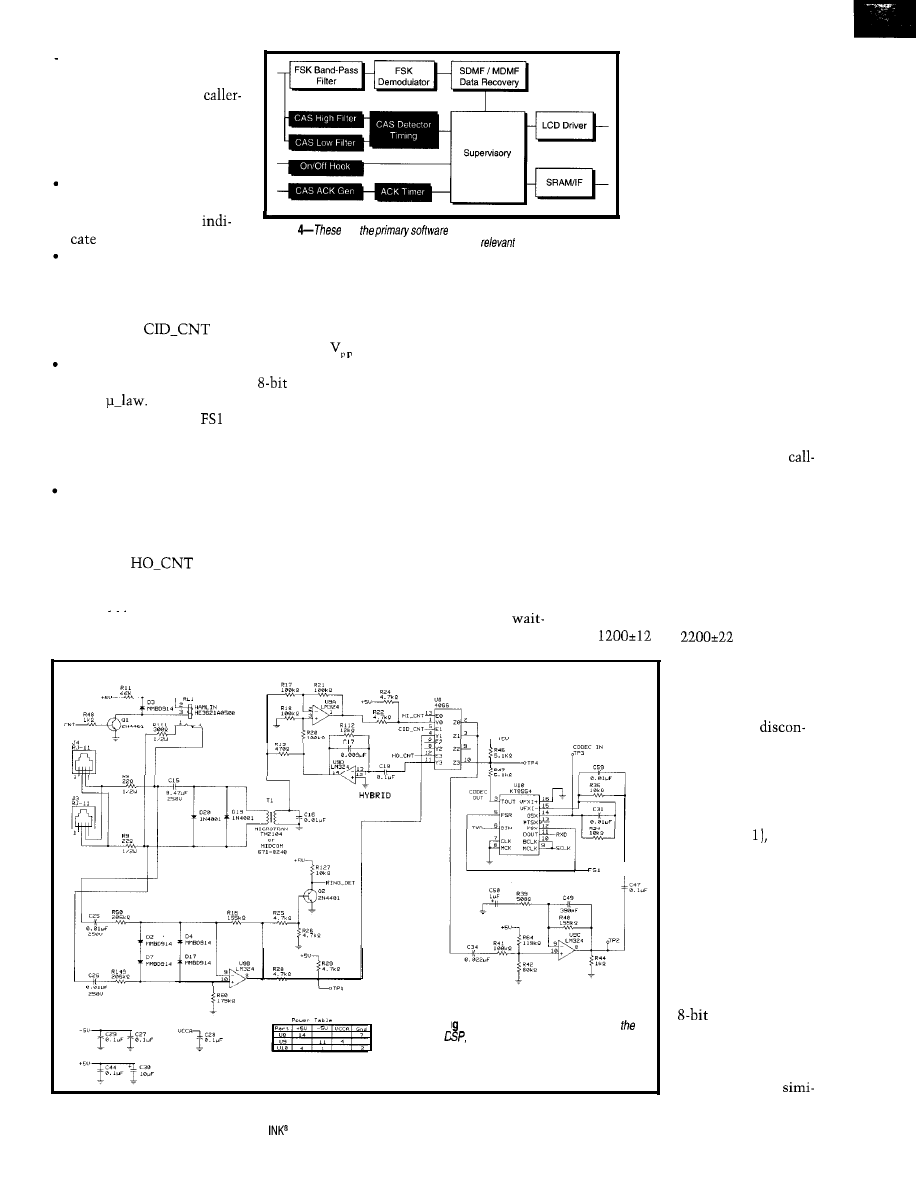
l
phone-line interface-includes
the transformer and compo-
nents that isolate the
ID circuits from the line (pro-
tects against damage from
the ring high-voltage signal)
and the on-/off- hook relay
ring-detect circuit-gives
digital input (
R I N G
_
D E T
signal) to the DSP to
rings on the phone line
Figure
are
functioning blocks with their rough
interconnection. Black areas illustrate the sections
fo off-hook connection.
caller-ID gain control-con-
trols signal gain coming from the
phone-line interface to the codec
analog input. The DSP enables this
path by the
control sig-
nal.
codec-acts as the DSP analog front
end. The codec data format is
PCM
The DSP controls the
sampling rate by the
signal and
serial shifts by SCLK signal. The
DSP receives serial data from RXD
and transmits serial data to TXD.
hybrid-The DSP sends the CAS
acknowledge via the codec and the
hybrid back to the phone-line inter-
face. The DSP enables this path by
using the
control signal.
The operation is relatively simple
. .
After power is applied and the reset
button pushed, the LCD should dis-
play “ready”. Check FSK levels on TP3.
The FSK signal’s amplitude should be
-3 when the FSK data is being
received between the first and second
ring. Adjust R3
1,
if necessary. Then,
read the LCD for the information.
OFF-HOOK DATA
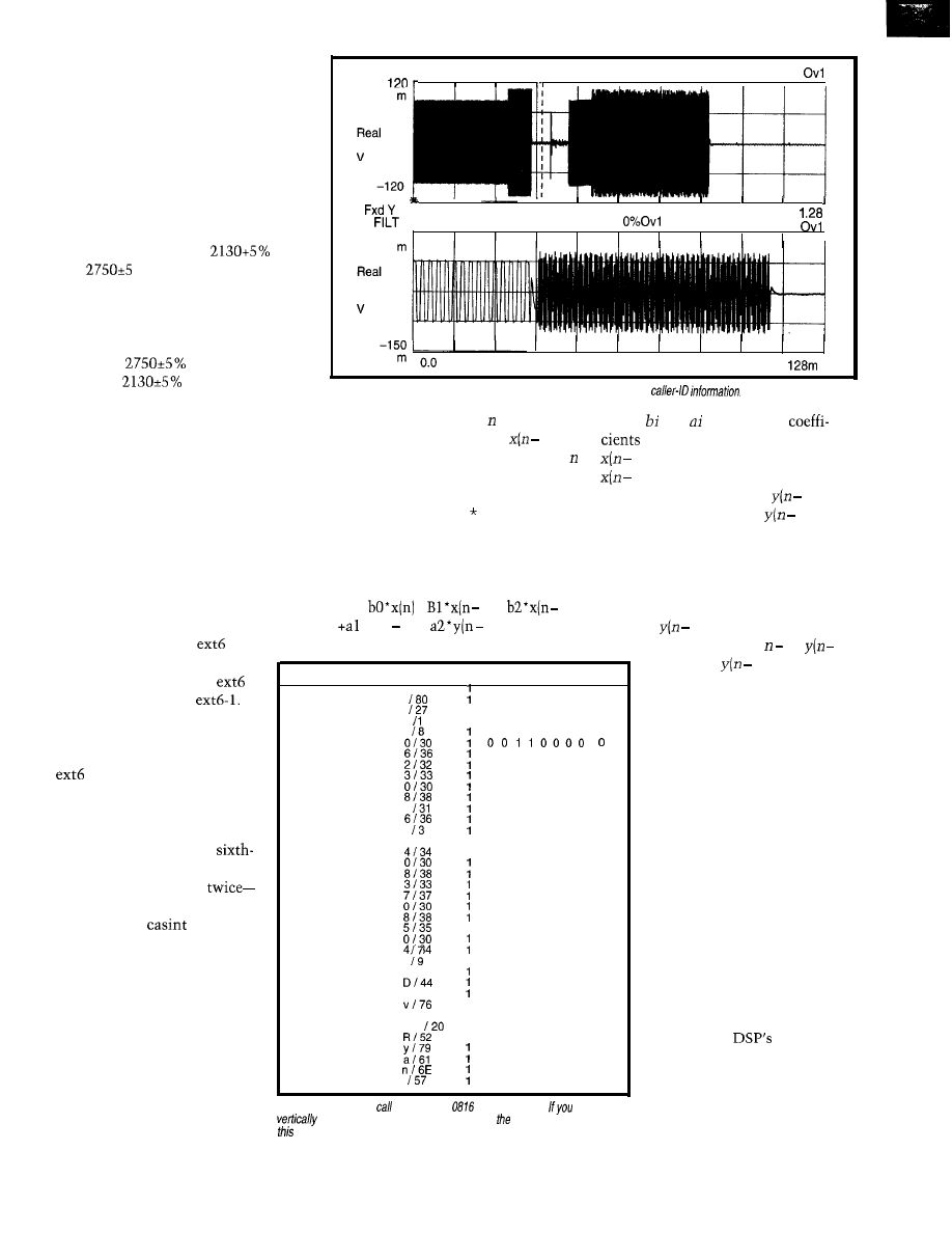
Figure 7 shows the delivery of FSK
data in the off-hook mode.
The larger amplitude, lower frequen-
cy waveforms at the beginning of CAP
TIM BUF are the call-waiting and CAS
tones. After a gap, the FSK data is seen.
During this gap, the DSP generatsby
an ACK. This ACK is not shown, as
the DSO was connected to the receive
Comparing the on- and
off-hook sections of Figure 4,
we see many differences. In
addition to the modules used
in on-hook selection, there’s
a CAS filter for the high- and
low- band portions of the
CAS signal, and special CAS
detector timing.
Once the CAS tone is
detected, an acknowledgment
must be returned via a DTMF
generator. It’s also necessary to deter-
mine if the system is on or off hook.
Operation in the off-hook mode is
not as simple, due to the extra com-
munication involved.
Connect P2 to line 2 or a CIDCW
simulator, if available. A simulator is
is mandatory for additional develop-
ment , since it involves a least 3 lines.
Again, a scope TP3 to check FSK
levels. On line 2, you should hear a
waiting tone followed by the special
CAS tone. If all is in order, the module
detects the tone, ACK is sent, and the
SPCS or simulator transmits data.
FSK DEMODULATION
A software FSK demodulation func-
tion is integrated into the DSP as you
and should be possible anywhere you
side. FILT TIME shows the call
can subscribe to caller ID.
ing and CAS tone in greater detail.
see in Figure 4. The FSK frequencies
are
and
Hz. After all
the protocol and hand-
shaking complete, the
data is sent using FSK.
This means there
are no phase
tinuities and only two
frequencies involved
in the FSK signal. The
lower frequency
1200 Hz represents a
mark (logic and the
higher 2200 Hz repre-
sents a space (logic 0).
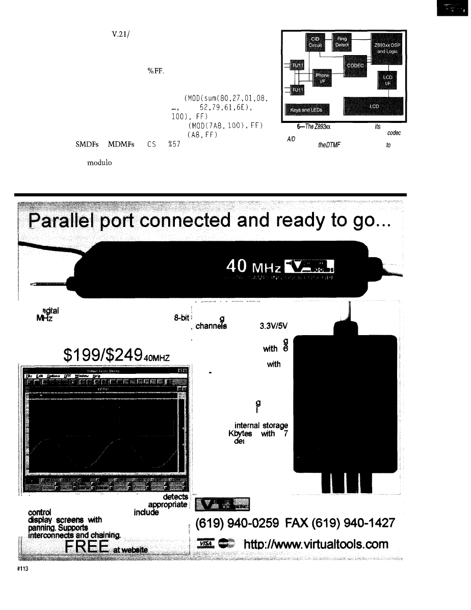
There is no parity
or error checking
beyond checking a
checksum sent at the
end of transmission. A
start bit (0) and a stop
Fi ure 5-The hardware connections of
AFE (Analog Front End), and line
interfaces are shown.
bit (1) added to each
transmitted
word.
The transmission
rate is 1200 bps and
demodulation is
22
Issue 83 June 1997
Circuit Cellar
lar to a standard low baud-rate
Bell 103 modem.
DATA RECOVERY
After FSK demodulation, the obvi-
ous concerns are the data format (see
Table 1) and how to decode it.
The message type is 80% (128 or
MDMF). Data therefore sent as param-
eter words where the parameter type
and length are binary and the calling
name and number are ASCII.
The last word of
or
is the checksum. The checksum is the
2’s complement of the
256
sum of the binary representation of all
other words in the message including
message type and length as well as the
parameter type and length.
Remove the start and stop bits. To
obtain the 2’s complement, XOR with
If you use Table 1 and hex calcu-
lations, the checksum is:
CS = XOR
20,
CS = XOR
CS = XOR
=
In a practical application, the calcula-
tion is less cumbersome due to the
natural modulo 256 nature of a byte.
Figure
DSP is shown with primary
links. The main route for DSP connection is the
or
and D/A connection through which the FSK data
is received and
tones are sent back the
central office or exchange.
Since there’s no error correction, the
practical application of the checksum
is to compare the received checksum
Our Di
Sampling Oscilloscopes have 20 or
40
maximum sampling rates with
resolution. Both have 32 Kbytes of storage; 7
sampling depths; 24 sampling rates; 6 input
voltage ranges; and multiple trigger options.
20 Ml-k
Our Lo ic Analyzer has 16
w i t h
compatible logic inputs.
The maximum samplin
rate is 40 MHz
internal clock rates and an
external clock input
+
or
going slope.
The
internal trigger
setup
allows bits to be low, high
or disabled. An external
logic level
tri ger
is
provided as wel
as the
ability to trigger from our
DSO. The
is 32
sampling
epths and 3
trigger position options.
Units can be chained for
larger data widths.
$199
Our Virtual Tools Bench software
connected devices and installs
surfaces, Features
4 data’
VIRTUAL TOOLS, Inc.
rapid zooming and,
up to 8 devices with trigger
Circuit Cellar INK@
Issue 83 June 1997
23
with the calculated one. If they don’t
agree, then the data is bad and should
generally not be displayed.
CAP TIM BUF
CAS DETECTION
A software CAS-detection function
is integrated into the DSP as shown in
Figure 4. It distinguishes the periodic
nature of the CAS tones from the ape-
riodic nature of voiced VOX.
0 . 0
TIME 1
160
p
CAS frequencies are
Hz
and
% Hz, making it a DTMF
signal. However, the CAS frequencies
are quite distinctly beyond the range of
normal signaling DTMF frequencies.
The signal is first filtered with CAS
high-filter
Hz and also CAS
low-filter
Hz. The resultant
outputs are rectified and tested for
minimum amplitude requirements.
Figure 7-/n the off-hook mode, the CAS signals the availability of
fhe
If requirements are met for both
frequencies, a timer checks for CAS
duration. For detection, the amplitude
must constantly exceed minimum
requirements for a period longer than a
predetermined gating limit.
The CAS-detector ISR services the
CAS detection (see Listing 1). This
portion first saves the accumulator and
status register, and then, the data is
retrieved from the codec.
data x(n) or data at time replaces the
where and are the filter
older x(n), which is saved as
1) or
and x(n) is the current sample.
the current sample delayed by 1 (i.e.,
1) is the previous sample, and
_ 1). This process repeats for all taps.
2) is the second previous sample.
Autoincrement performs filter
y(n) is the current output,
1) is
computations (coeff sample).
the previous output, and
2) is the
Also, a single-cycle M PY A (multiply
second previous output.
and accumulate) instruction is used.
The last code section updates the
The fundamental equation is:
output taps or delays in time. The
newest output y(n) (i.e., output data at
y(n) =
+
1) +
2)
time n) replaces the older y(n) and is
*y(n 1) +
2)
saved as
1) or the current output
The codec register
is
double buffered, which means
that there are really two
registers-extb-0 and
The assembler only reads ext6,
which is why we have an ap-
parently redundant load of
to push the data out.
Next, the filters are called.
Since the biquad structure is
used, the filters are called
three times to give a net
order filter.
This process repeats
once for each filter. The final
portion of the
ISR re-
stores the accumulator and
status register.
The basic biquad structure
filters the core. This portion of
the code is structured so the
tap updates and actual filter
calculations are performed
within the b i qua d subroutine.
The first section of this
Bit (MSB-LSB)
ASCII/HEX% Stop 7 6 5 4 3 2 1 0 Start
Message Type
1 0 0 0 0 0 0 0
0
Message Length
0 0 1 0 0 1 1 1
0
Parameter Type
1
0 0 0 0 0 0 0 1
0
Parameter Length
0 0 0 0 1 0 0 0
0
Month
0 0 1 1 0 1 1 0
0
Day
0 0 1 1 0 0 1 0
0
1
0 0 1 1 0 0 1 1
0
Hour
0 0 1 1 0 0 0 0
0
0 0 1 1 1 0 0 0
0
Minute
1
0 0 1 1 0 0 0 1
0
0 0 1 1 0 1 1 0
0
Parameter Type
0 0 0 0 0 0 1 1
0
Parameter Length
/ A
0 0 0 0 1 0 1 0
0
DN
4083708504
1
0 0 1 1 0 1 0 0
0
1
0 0 1 1 0 0 0 0
0
0 0 1 1 1 0 0 0
0
0 0 1 1 0 0 1 1
0
0 0 1 1 0 1 1 1
0
0 0 1 1 0 0 0 0
0
0 0 1 1 1 0 0 0
0
0 0 1 1 0 1 0 1
0
0 0 1 1 0 0 0 0
0
0 0 1 1 0 1 0 0
0
Parameter Type
1
0 0 0 0 0 1 1 1
0
Parameter Length
0 0 0 0 1 0 0 1
0
CN Dave Ryan
0 1 0 0 0 1 0 0
0
a / 6 1
0 1 1 0 0 0 0 1
0
0 1 1 1 0 1 1 0
0
e / 6 5
1
0 1 1 0 0 1 0 1
0
Space
1
0 0 1 0 0 0 0 0
0
1
0 1 0 1 0 0 1 0
0
01111001 01100001
0 0
0 1 1 0 1 1 1 0
0
Checksum
0 1 0 1 0 1 1 1
0
code updates the input taps or
Table l--This
traces a by Dave at
AM on June 23.
follow
delays. The newest sample of
down the second column, you can see
individual elements of
transaction byfe by byte.
delayed by 1 (i.e., 1).
1)
is saved as
2). The process
is repeated for all output taps.
DISPLAY DRIVERS
Our display is a off-the-shelf
dot-matrix LCD with 16 char-
acters x 4 lines. It is logically
organized with 2 lines of 32
characters which overrun. It
can display any ASCII charac-
ter and many other characters.
The low-level drivers and
controller are mounted on the
LCD module. You just need a
relatively simple high-level
software driver to instruct the
LCD which character to dis-
play and where to place it.
The DSP bit bangs the
ASCII data to the LCD control-
ler using the
external
data bus. The LCD is a rela-
tively slow device, far slower
than normal DSP operations,
so updating the LCD presents
minimal overhead to the DSP.
24
Issue
83
June 1997
Circuit Cellar INK@
Listing
base filter’s b qua
may be used for a great
variety
of
Of course, filter
coefficients
must
be
each case. the
single-instruction
Sixth-order triple biquad IIR filter
a
with address
for input samples
to input sample
a
for filter coefficients
to filter coefficients
new input sample
new
input sample
to
u-law data to accumulator
Ulaw
:u-law result is
sign magnitude number
sll a
left logical, multiply by 2
sll a
left logical, multiply by 2
x,a
= new data
tempist,a
temporary input storage
call biquad
standard biquad
call biquad
standard biquad
call biquad
standard biquad
save output filter response
third-stage output
output
auto hardware u-law
endinti:
ret
from
ISR
biquad:
filter computations
* sample) using autoincrement
=
+
+
+
New Sample is in x, Output is in
update input sample buffer
saves old
pO:O points at
= new sample
pO:O points at
saves old
points at
=
saves old
points at
=
a,pO:O
points at (n-2)
sub
pO:O,a
points at
+
+
+
;A= 0 P =
*
=
mpya
* X12
Xl2 =
mpya
* Xl3
Xl3 =
mpya
*
=
mpya
* Y12
=
add
result of last multiply to
sll a
back if divide by 2 on coefficients
result in x
output buffer
a,pO:O
points at
sub
a,#%2
pO:O,a
;pO:O points at
saves old
= new result
=
=
output filter response
stage output
ret
from biquads
Communication is done via a
When the SDMF or MDMF data is
cialized series of LCD instructions.
received, it should be displayed. A
Once the LCD is initialized, the data is
state machine takes care of the logical
transmitted.
progress of the call. At the end of the
call, a disconnection occurs and the
CALL PROGRESS
entire cycle repeats.
Call progress is sequential. A ring
must be detected first. Once the call is
MEMORY STORAGE
established, only one of two events can
Again, due to the multitasking
happen-either a call interrupt occurs
features common to
normal call
or does not occur.
progress, especially on-/off-hook moni-
toring, system supervision, memory
for calls received, and display tasks,
can be handled by a single DSP.
For the sake of simplicity, we didn’t
add memory storage to this demo. The
external bus addressing capability
enables this feature to be easily added.
TAKE IT FURTHER
The system described is elemental.
Many value-added features are possible
(e.g., ring only on certain callers). Such
features are easily added as controller
functions.
Just let your imagination lead..
q
Dave Ryan is a systems engineer in
Zilog’s data communications. He
works on their next-generation
fixed-point processor-class device. You
may reach Dave at
Hazanchuk works in SDP sys-
tem engineering and applications at
Zilog. He has 15 years of DSP experi-
ence in image processing and com-
pression, digital answering machines,
cell phones, caller ID, magnetic-stripe
readers, and DSP architectures.
The complete code for this article is
available on the Circuit Cellar Web
site.
J.D. Gibson, Principles of Digital
and Analog Communications,
MacMillan, New York, NY, 1993.
Bellcore, Technical Reference
NWT-000031 and NWT-001188.
Bellcore, Generic Requirements
30-CORE.
Bellcore, Special Reports
002578 and SR-TSV-002476.
Zilog
2 10 Hacienda Ave.
Campbell, CA 95008-6600
(408) 370-8000
Fax: (408) 370-8056
404 Very Useful
405 Moderately Useful
406 Not Useful
Circuit
Cellar INK@
2 5
Chris Sakkas
PC Telephone Interface
’
fascinating applica-
tions beyond simple voice mail. Com-
puter telephony also includes complete
interactive voice-response systems, call
processing, autoattendants, and more.
As well, computer telephony integra-
tion can lead to interesting applications
involving remote access to computer
control and home-automation systems.
In this project, a low-cost ISA expan-
sion card serves as a complete tele-
phone interface. It records and plays
back messages, decodes touchtones,
dials, and handles switch-hook control.
I also discuss software for develop-
ing a nine-mailbox voice-mail system.
This software-hardware combination
is a useful base for creating applications
for voice messaging, call processing,
home automation, and more.
CONCEPT
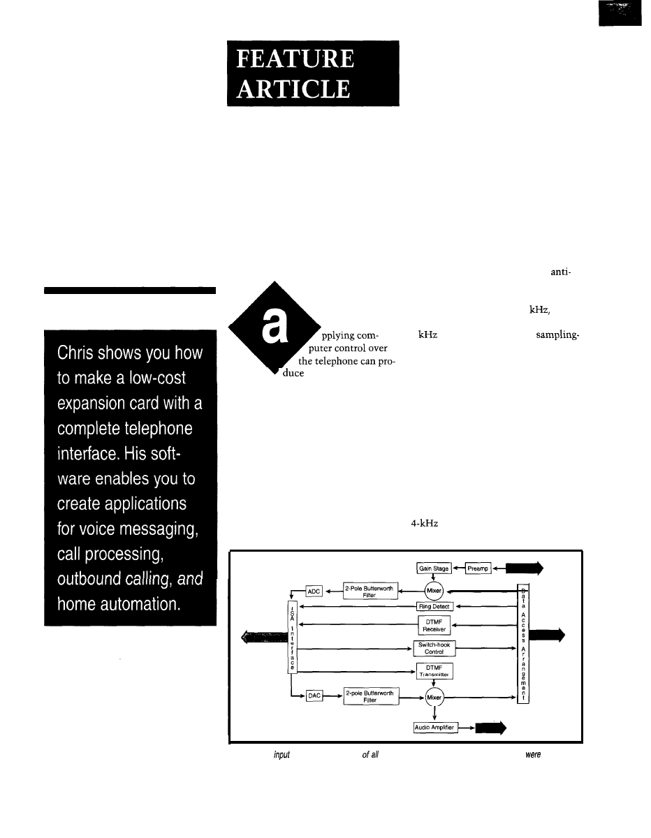
Figure
1
outlines the hardware de-
sign, showing the telephone input to
the card as well as the I/O and func-
tional relationship of individual items.
The Data Access Arrangement takes
telephone input and passes it to a sum-
ming amplifier to mix the signal with
the microphone input. This input is
amplified to a level ready to sample via
the preamplifier and a second amplifier.
The signal is fed through the
aliasing low-pass filter and sampled by
the ADC. Since the phone system
bandwidth is limited to -4
the
sampling frequency must be at least
8
to satisfy the Nyquist
frequency theorem. The CPU gets this
data byte via the ISA interface.
After the DAC converts PC data to
analog form, the signal is fed into a
reconstruction filter and then mixed
with the DTMF transmitter output.
An audio amplifier amplifies the signal
into levels capable of driving a speaker.
SPECIFICATIONS
The hardware needed to handle
8-bit A/D and D/A conversions, as
well as DTMF tone decoding and trans-
mission. It had to be able to sample a
signal, and its data storage rate
was limited to at most 8 kbps.
Figure l--The
and output relationship
subsystems is shown. Many of the subsystems
implemented
in sing/e monolithic devices.
26
Issue 83
June 1997
Circuit Cellar INK@
As well, it needed an
RJ-11
line connection and a user-selectable
port address. Finally, it had to satisfy
FCC Part 68 requirements.
To minimize components, com-
plexity, and cost and maximize the
hardware’s flexibility, I chose highly
integrated components to handle the
interface logic, A/D and D/A conver-
sions, DTMF decoding and transmis-
sion, and telephone-line interfacing.
HARDWARE
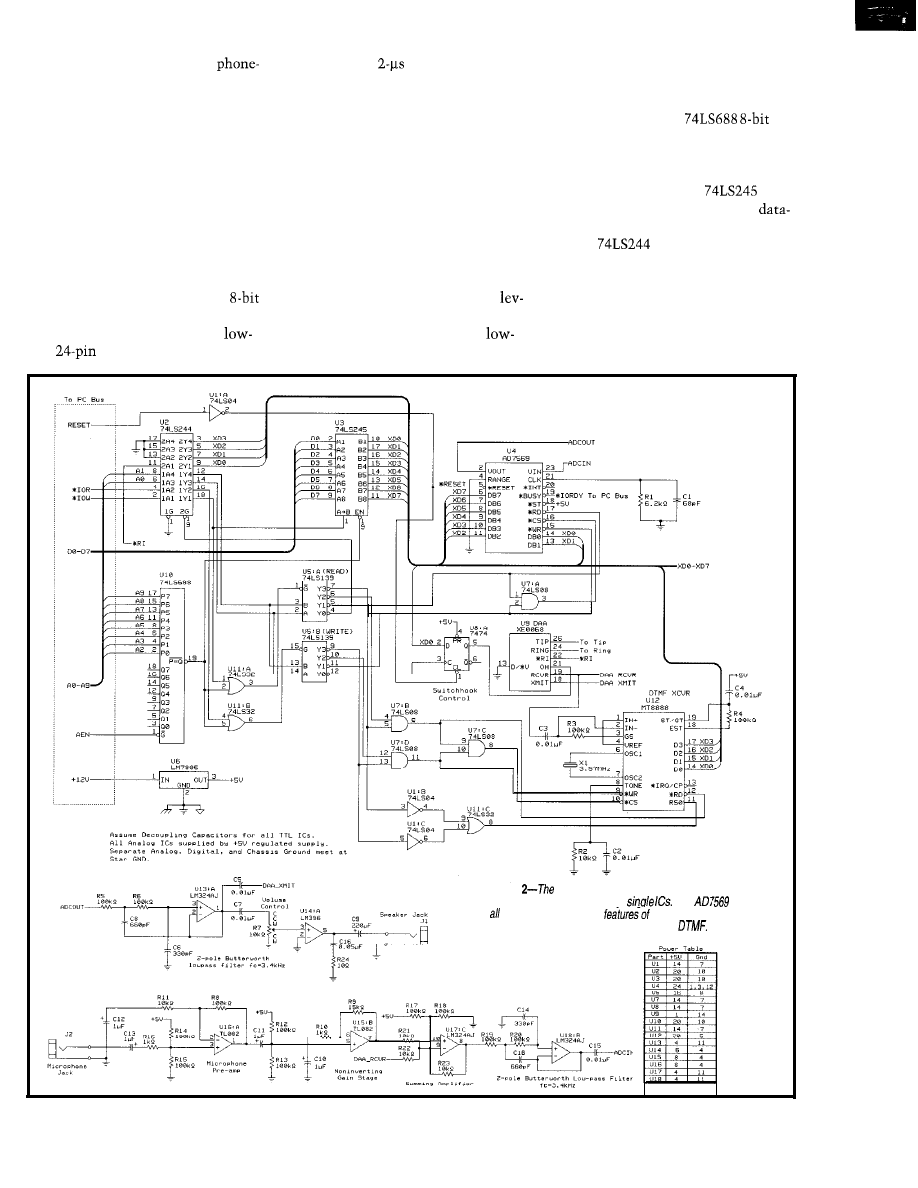
The Xecom XE0068 Data Access
Arrangement provides TTL-level ring
detection and switch-hook control.
The internal Automatic Gain Control
(
A G C
) circuit optimizes transmit
The
also buffers between
the bus and hardware, the I/O read and
write lines, and the two least signifi-
cant bits of the address bus. These bits
The Analog Devices AD7569
Analog I/O system provides fast A/D
els and maintains a small package size.
are needed for decoding which of .the
and D/A conversion in a small,
This device provides a legal,
four port addresses is to be used for
cost
package. It has a minimal
cost interface to the phone system with
hardware access.
bus interface,
conversion time,
and single supply voltage, which ac-
cepts several ranges of input voltages.
The Teltone M-8888 DTMF trans-
ceiver handles DTMF tone decoding
and transmission. This 20-pin package
provides easy interfacing with a micro-
processor and has a call-progress mode.
(It works with a single supply voltage.)
its FCC Part 68 registration. The regis-
tration transfers to the end application.
Figure 2 shows the schematic for
the interface card. A
comparator is used as a decoder for the
board. When an address corresponding
to the card’s base port address is de-
tected, the enable of the
octal
bus transceiver is selected so the
bus contents can be accessed.
Figure
schematic of the PC telephone interface shows
many functions are handled by
The
handles
sampling and
playback
the card,
while the
M-8888 handles encoding and decoding of
Circuit Cellar INK@
Issue 93 June 1997
2 7
R
A
T
I
O
N
S.P.D.T.
snap-action switch with
roller positioned above switch
actuator. Rated 5 amps
Switch body:
0.63” x 0.375”. Solder or qc
terminals.
UL
and CSA listed.
SMS-1
Nichicon
MHSC
1.375” diameter x high.
0.4” lead spacing.
EC-4745
Semi-circular, irregularly-shaped magnets.
Shiny finish with a polarity marking dot.
0.93” long x 0.3” x 0.07” thick.
Powerful for their size.
CAT#
PCS
. $100.00
7 blade, mini 12
on a heatsink.
Assembly is 2”
sauare X
a 0.87” square flat
area on side opposite fan
from which fins radiate. One fin
extends 0.63” beyond the others. Includes
two mounting clips.
CAT # CF-40
TERMS: NO MINIMUM ORDER
and
for the
IS
U.S.A. $5 00 per order. All others including AK,
HI.
PR or Canada must pay lull shipping. All orders delivered
CALIFORNIA must include local state sales tax. Quantities
CALL,
NO COD Prices subject
to
FAX
or E-MAIL
for
our
without
96
CATALOG
Outside the
send $3.00
Port
Bit
Read
Write
$300 0
Ring detect (0 = ring)
Hook switch (0 = on, 1 off)
$301
O-7 ADC read
DAC write
$302 O-3 Read DTMF receiver
Write to DTMF transmitter
$303
O-3
Read DTMF status register bit Write DTMF control register
l-Four PC
are used for the card. Additional functionality can be added to the card and
via
the first
address
The
consists of two 2-to-4
decoders, each supplied with
and
Al of the address bus. The appropriate
portion for reading or writing is en-
abled, depending on the status of the
and ‘IOW bus lines.
The base address of $300 (hex) is
used, but any nonconflicting address is
possible. Changing the address means
pins 16 and 18 of the
should
be tied high. The rest should be low for
this addressing example. Table 1 lists
the port addresses and functions.
Depending on the action taken by
the
the appropriate compo-
nent is enabled-either the AD7569
for read or write or the M-8888 for
read, write, or register selection.
It can also read the contents of the
Ring Indicator pin via the
second half of the
Or, it can
toggle the hook switch by changing
the contents of the
D-type
flip-flop [which acts as a I-bit register).
The AD7569 converts data when
it’s selected and the l RD (read) pin is
strobed. The IC activates its *BUSY
line, which is connected to ‘IORDY
on the PC bus. This action extends the
read’s bus cycle if necessary to the
amount needed for a read to occur.
Due to the relatively low sampling
frequency, I didn’t use precise timing
circuitry. All timing was done via the
PC’s programmable interval timer.
In a PC-compatible system, this
timer has three different channels, and
channel zero is the system clock-tick
timer. The ROM BIOS programs the
timer to generate an interrupt 08 at a
frequency of 18.2 times per second.
For most systems, however, this
frequency can be reprogrammed to
occur at a much greater rate, making it
more useful for this project. Software
can reprogram the timer and still main-
tain the proper call to other service
routines 18.2 times per second.
I chose a microphone preamplifier
based on a noninverting amplifier
using one-half of a TL082 operational
amplifier. The op-amp is biased to
operate from a single 5-V supply, as are
all other op-amps in this design.
The preamp provides a
gain.
This low-level signal is amplified again
by the second-half of the TL082 op-amp
configured as another noninverting
amplifier with a gain of 23.5
I chose National Semiconductor’s
TL082 JFET input operational ampli-
fier for its high input impedance, low
noise voltage, and low input bias cur-
rent. These features make it ideal for
converting a microvolt signal to a
millivolt signal.
A summing amplifier mixes out-
puts from the microphone amplifica-
tion circuitry and the DAA’s receiver,
using one-fourth of an LM324 op-amp.
The summing amplifier’s output is
applied to a two-pole Butterworth
pass filter before entering the ADC.
A second summing amplifier mixes
the DAC and DTMF outputs. A
pole Butter-worth low-pass filter acts as
a reconstruction filter for this signal.
Both filters in this design are identi-
cal and are based on the popular
gain
and Key configuration. I
use National Semiconductor’s LM324
quad op-amp for both since it is low
cost and has four op-amps per package.
The filters were designed for a
cut-off frequency, appropriate for filter-
ing out aliasing signal elements for
this application.
The reconstruction filter output is
applied to the DAA’s transmit pin and
the input of the LM386 audio ampli-
fier. The LM386 amplifier provides
adequate audio amplification in a
cost monolithic package. The audio
output connects to a jack on the back
of the card.
SOFTWARE
Voice data is managed by a message
structure,
(see
Web site for
source code). It stores a pointer to the
28
Issue 83
June 1997
Circuit Cellar
actual voice message data, the number
of data bytes, an indicator of whether
the data is in memory or stored on disk,
a message description, and a filename.
An enumerated type, b i
a us,
is defined with on and off for Boolean
control. The software has functions
that can be integrated into other pro-
grams to incorporate telephone sup-
port. The routines are divided into
telephone-control, message record and
playback, and DTMF functions.
Telephone-control functions
cludeWaitForRing,HookSwitch,
and RingDetect.WaitForRing waits
for an incoming number of rings based
on the variable co n Control goes to
the calling function after the specified
ring number is encountered.
tch simply controls the
telephone’s hook-switch status, either
on or off. Ri
returns on if a
ring is detected and off otherwise.
Read F i
1 e,
a message record and
play-back function, reads a specified
filename into memory for playback.
Play-MessageandRecordMessage
expect a me s
structure to be passed
to begin playback or recording. The
PC’s programmable interval timer is
used for machine-independent timing.
DTMF initialization is performed
via DTMFInit.DTMFReceive and
read or place the DTMF
character in the M-8888 buffer. DTMF
Transmit mustbesetupwithacall
function.
With these functions, I developed a
small voice-mail application for nine
mailboxes. After a main greeting and
the individual voice message for each
mailbox is played, the user may record
a message at the tone.
The main greeting is contained in
the file G R E ET MN. Mailbox greetings
are contained in G R E ET where
denotes the mailbox number. A re-
ceived message is stored in M ES G E
This entire application was coded in
-60 lines of C code.
Several example programs show
further potential uses of the card. These
programs can record to a file, playback
a file, and act as a telephone dialer.
INTERFACING IDEAS
The PC-telephone interface pro-
vides an easy way to interface a
compatible computer to the telephone
network. Other more sophisticated
applications can be developed, includ-
ing many beyond typical
telephony applications.
A home-automation or other com-
puter-controlled system can be modi-
fied to receive commands and deliver
reports remotely. With added circuitry,
a complete amateur-radio repeater
controller can be created with voice
and sophisticated computer control.
q
Chris Sakkas is president of ITU Tech-
nologies, a company specializing in
development tools for microcontrol-
lers. You may reach him via E-mail at
or by telephone at
(513) 574-7523.
The complete source code for this
article can be downloaded from the
Circuit Cellar Web site.
AD7569
Analog Devices
One Technology Way
MA 02062-9 106
(617)
Fax: (617) 329-1241
M-8888
Teltone Corp.
22121 20th Ave. SE
Bothell, WA 98021
(206) 487-1515
Fax: (206) 487-2288
XE0068
Xecom
374 Turquoise St.
Milpitas, CA 95035
(408)
Fax: (408)
1346
TL082, LM324, LM386
National Semiconductor
P.O. Box 58090
Santa Clara, CA 95052-8090
(408) 721-5000
Fax: (408) 739-9803
407
Very Useful
408 Moderately Useful
409 Not Useful
Your PC Development Tools
No
M
ORE
C
RASH
B
URN
EPROM
Technology
DOS Single Board Computer
572
FLASH Memory disk drive
10
Mhz CPU 2 Timers
512 k bytes RAM
4 Interrupt Lines
512
k FLASH 8 Analog Inputs
2 Serial Ports
X-Modem File
24 Parallel Lines
Transfer
INCLUDES DOS Utilities
8 Channels,
6 Conversion Time
Option
Includes Drivers
Apps.
4 8
Inputs
JK micros stems
Cost Effective Control ers for
TO ORDER (510) 2364151
FAX (510)
Visit
our WEB site-www.dsp.com/jkmicra
1275 Yuba Ave., San Pablo, CA 94806
Circuit Cellar INK@
Issue83
June1997
29
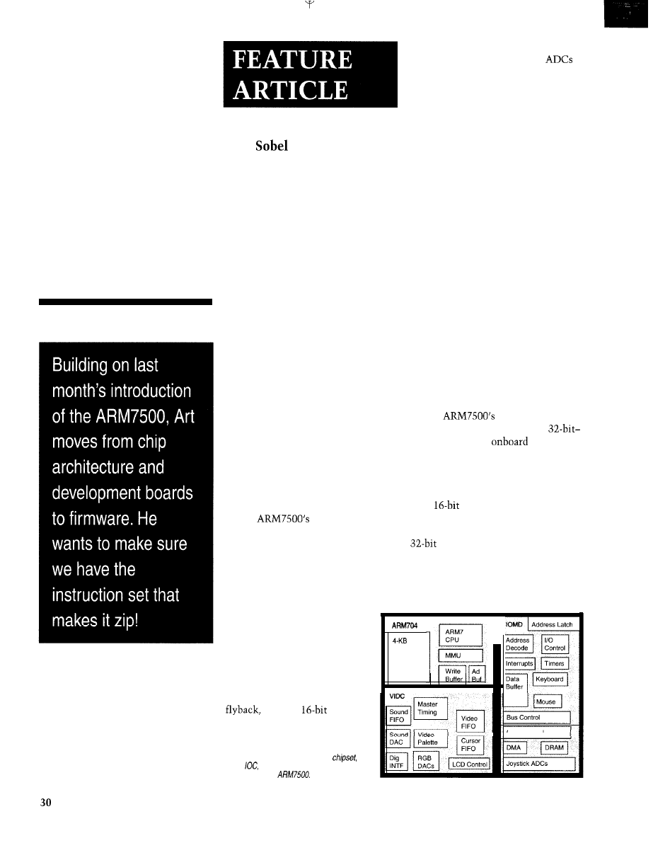
Art
Embedding the ARM7500
Part 2: Programming an
Embedded Computer
0
he ARM7500 is
exceedingly compli-
cated, having similar
resources to a typical PC’s
CPU and motherboard logic. After
building the development board, my
first task was porting the C-Demon, a
ROM-based monitor used in other
ARM development boards.
Demon initializes the ARM and
peripheral registers, builds a compatible
memory map for monitor variables, and
starts communication with the host.
After the C-Demon was working,
each major chip section needed drivers.
These drivers are wrapped up in the
console test program.
The
ROM controller
resets to 16-bit mode. I chose a
wide ROM for the
software.
This switch was a bit tricky as the
ARM program counter nearly always
fetches two instructions ahead of the
execution unit.
The
CPU and MEMC
memory, I/O, and VIDC video/sound
controllers were conserved from the
original Acorn computer, keeping the
original OS and user software some-
what compatible.
From a programmer’s view, the
ARM7500 functional blocks are
separate sets of registers incorpo-
rated in the memory map as
shown in Figure 1.
In
mode, the memory control-
ler accesses the low and then the high
16 bits and presents the assembled
word to the instruction unit. In
Listing 1 (Level 0 code), the first 14
entries have the upper 16 bits zeroed.
The ROM start-up code is hand
assembled since the rest of the code is
Cache
As Table 1 shows, the IOC
handles internal peripherals like
keyboard and mouse control, 11
general-purpose I/O pins, video
and two
timers. It
Figure l-Acorn’s former discrete
CPU,
MEMC, and V/DC are preserved in
the layout of the
also controls six sets of interrupt-con-
trol registers, four single-slope
for the joystick interface, memory and
I/O timing, as well as ROM and DRAM
width.
Lastly, the IOC has registers control-
ling the clocks. The CPU clock can be
turned off, or the whole chip can have
clocks suspended.
The external clock can also be con-
trolled. In stopped mode, an external
clock/calendar restarts the chip by
grounding one of two special interrupt
pins.
The DMA channels were histori-
cally part of the MEMC. The basic
DMA channels are retained in the
ARM7500 (see Table 2).
The myriad video-timing registers,
pixel control, and clock control, as
well as the analog sound clock and
steering register are placed in the VIDC
functional block (see Table 3).
C-DEMON PORTING
Clock Control
Issue 83 June 1997
Circuit
Cellar
INK@
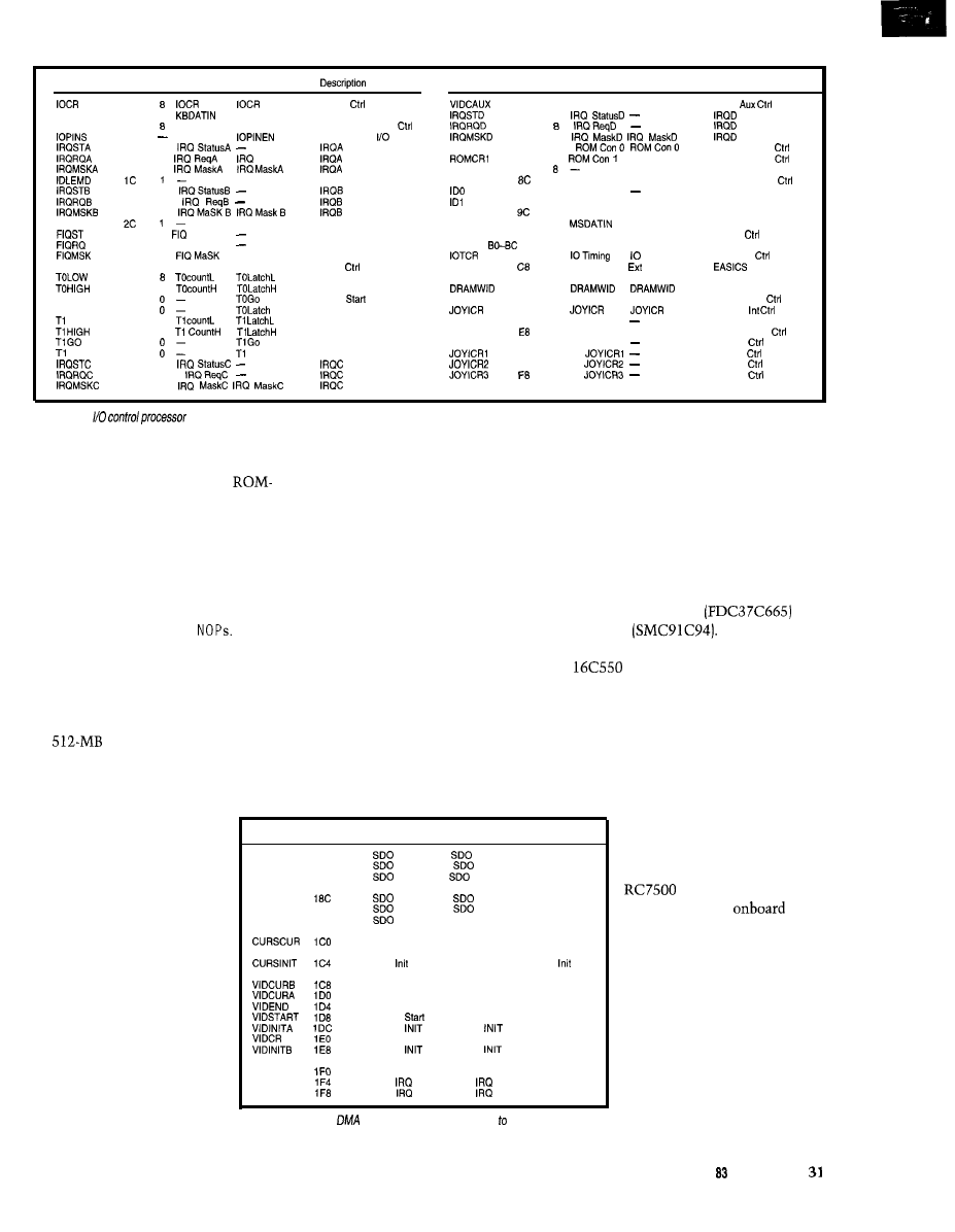
Name
Address Size Read
Write
Name
Address Size Read
Write
00
I/O Pin
6C
8 V I D A U X
VIDAUX
KBDAT
04
8
KBDATOUT
Keyboard Data
70
8
KBDCR
08
K B D C R
KBDCR
Keyboard Stat and
74
o c
IOPINS
8 Open-Drain
Pins
78
8
10
8
Stat
ROMCRO
80
8
14
8
clear A
Req
84
8
ROM Con 1
18
8
Mask
RESV
88
Enter IDLE MODE
CPU Idle Cmd
RFSHCR
8 Refresh CR
Refresh CR
20
8
Stat
94
8
Chip ID L byte
24
8
Req
98
8
Chip ID H byte-
28
8
Mask
VERSION
8 Chip Version
STOPMD
Enter STOP MODE Clock Stop Cmd
MSDAT
A8
8
MSDATOUT
30
8
Status
FIQ Stat
MSCR
AC
8 M S C R
MSCR
34
8 FIQ Req
FIQ Req
reserved
38
8
FIQ Mask
FIQ Mask
c 4
8
Timing
CLKCTL
3C
8 C L K C T L
CLKCTL
Clock
ECTCR
8
Ext IO Timing
IO Timing
40
Tmr 0 Latch Data Low
ASTCR
c c
8 A S T C R
ASTCR
44
8
Tmr 0 Latch Data High
D
O
8
TOGO
48
Command
Tmr 0
SELFREF D4
8 SELFREF
SELFREF
TOLAT
4c
Tmr 0 Latch Cmd
E O
8
LOW
50
8
Tmr 1 Latch Data Low
JOYSR
E4
8 JOYSR
54
8
Tmr 1 Latch Data High
JOYCC
8 J O Y C C
JOYCC
58
Tmr 1 Start
JOYCNTO
E C
1 6 J O Y C N T O
LAT
5c
Latch
Tmr 1 Latch Cmd
F O
16
60
8
Stat
F4
16
64
8
Req
16
68
8
Mask
reserved FC-17C
Description
Video
Stat
Req
Mask
ROM 0 Timing
ROM 1 Timing
DRAM Refresh
Mouse Data
Mouse
and Stat
IO Timing
Timing
Ext MEMC Timing
DRAM Width
Self Refresh
Joystick
Joystick Stat
J o y s t i c k
Joystick
0
Joystick
1
Joystick
2
Joystick
3
Table l--The
registers manage the keyboard, mouse, interrupts, timer, joystick, and memory-control functions.
in normal 32-bit format. The code loads
After RAM size is found and the stacks
a protected-mode ‘x86 processor with
an immediate value for the internal I/O
for the various ARM operation modes
all its hardware interrupt-assist logic.
controller address and the new
controller value, and then loads it into
the ROM controller.
are initialized, the cache is enabled.
After this code, the PC is directly
loaded with 0. Although the ROM
controller s t 0 r e instruction is written
before the jump, it executes afterwards.
The start-up code is reinterpreted in
32-bit mode as a series of
The next task is programming the
internal registers for the interrupts,
timer, and other functions (see Table 1).
The interrupts differ greatly from
the previous ARM600 PID port. The
ARM7500 has five IRQ (normal inter-
rupt) and one FIQ (fast interrupt) regis-
ters. Thus, the processor reads up to
five 8-bit registers to find out which
interrupt caused an IRQ and one 8-bit
register to locate the FIQ source. Each
interrupt request register is read and
each bit is examined for the first set bit.
The ARM7500 has two 16-bit timers
operating at 2 MHz (with a 32-MHz I/O
clock). To produce an -lOO-Hz continu-
ous interrupt every 10 ms, the 2 MHz
is divided by 20,000.
Communications with the host are
accomplished via the serial port on the
PC I/O Combo chip
or
Ethernet
The next trick is to remap the mem-
ory using the MMU (see Table 4). I took
advantage of the ROM being mapped
to 0 and also mapped to 0x20000000,
since the physical memory map repeats
on
boundaries.
The I/O Combo’s serial port is
compatible, so the code used
in the previous PID board works but at
a different address.
The program jumps to the higher
ROM location and initializes the MMU
page-table pointer to a precalculated
primary page table at the end
of ROM. The cache remains
off so the RAM size may be
determined.
This bit’s location indexes into a
table of interrupt routines. Despite such
complexities, the ARM7500 can handle
the interrupt routine much faster than
The next steps to start the Demon
are common to all versions. You set up
data structures in low-memory RAM,
check ROM for the correct checksum,
and send a banner message to the host.
Since the actual RAM is
smaller than the huge space
allotted (64 MB in each bank),
the physical RAM repeats
several times. The RAM size
is found by detecting the
rollover to RAM address 0
when its size is exceeded.
When cache is enabled,
figuring out RAM size be-
comes a problem. The cache
tag thinks address 0 is still
valid even though it’s over-
written from a higher address.
Name
Address Size Read
Write
Description
SDOCURA
180
32
0 Current A
0 Current A Ch A Current
SDOENDA
184
32
0 End A
0 End A
Ch A End
SDOCURB
168
32
0 Current B
0 Current B
Ch B Current
SDOENDB
32
0 End B
0 End B
Ch B End
SDOCR
190 8
0 Control
0 Control
Sound Control
SDOST
194
8
0 Status
Sound Status
32 Curs Current
curs current
32 Curs
Curs
32 VIDEO Current
VIDEO Current B
32 VIDEO Current
VIDEO Current A
32 VIDEO End
VIDEO End
32 VIDEO
VIDEO Start
32 VIDEO
VIDEO
A
8
VIDEO Control
VIDEO Control
32 VIDEO
VIDEO
B
DMAST
8
DMA Status
DMARQ
8
DMA
Req
DMA
Req
DMAMSK
8
DMA
Mask
DMA
Mask
Table 2-ARM7500
registers are loaded according
their state diagram in
Figure
4.
CONSOLE TEST PROGRAM
The console test program
checks the functions of the
and ARM7500, as well
as the additional
logic.
Source code for all tests helps
you get a feel for the software
drivers (see Listing 2). When
the console program is run,
Figure 2 appears onscreen.
RAW VIDEO
Getting video comes first.
Without a functional display,
no progress is possible.
The ARM7500 video regis-
ters are in Table 3. The display
Circuit Cellar
INK@
Issue June 1997
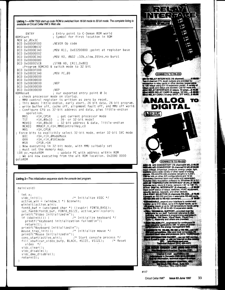
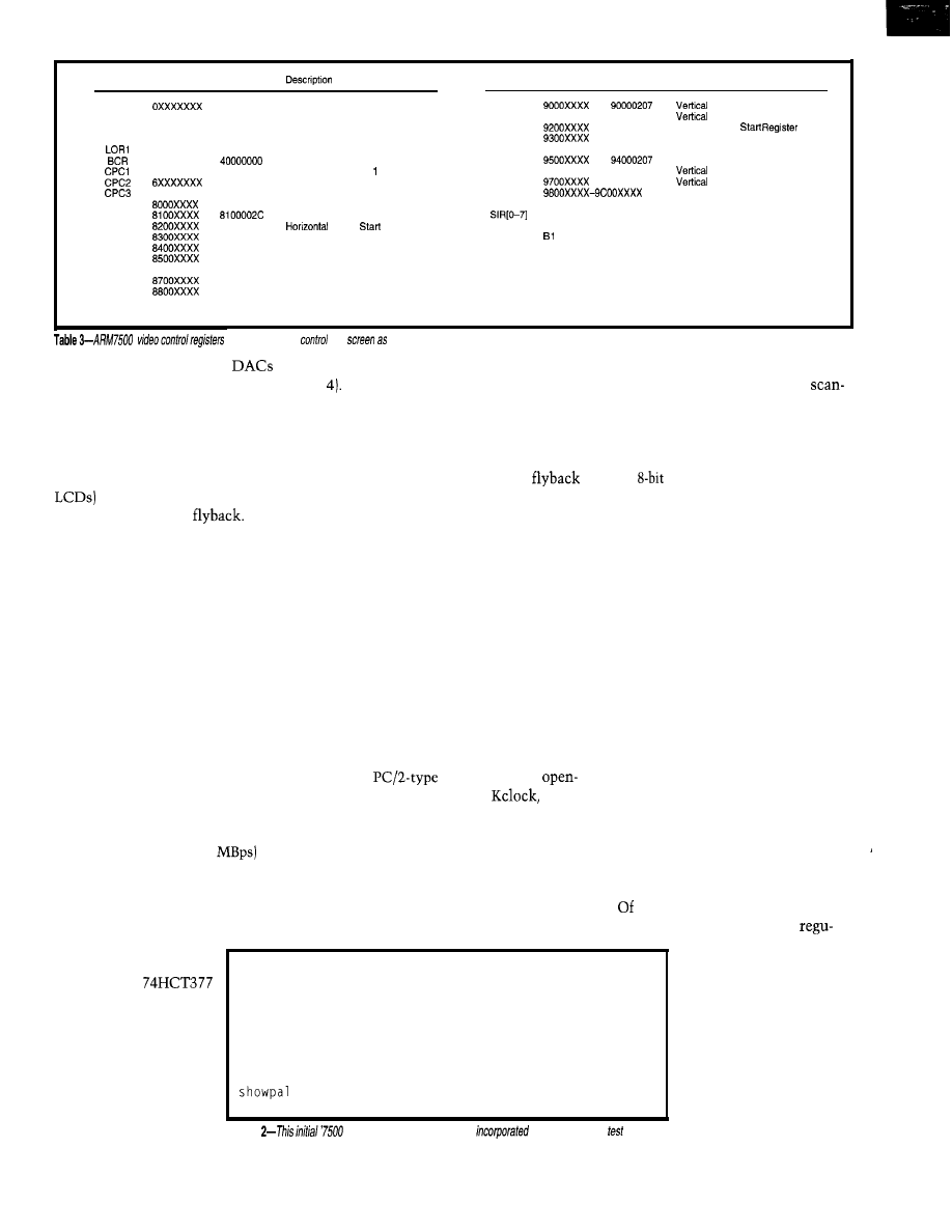
Register
Data
VGA Value
Register
Data
VGA Value
Description
VP
VPAR
LORO
HCR
HSWR
HBSR
HDSR
HDER
HCER
HCSR
1 oooooxx
2 x x x x x x x
3oooooxx
310000xx
4 x x x x x x x
5 x x x x x x x
7 x x x x x x x
8600XXXX
8900XXXX
8COOXXXX
80000336
82000072
83000080
84000300
85000324
8600007f
Video Palette
Palette address
Resewed
LCD Offset Register 0
LCD Offset Register 1
Border Color
Cursor Palette Color
Cursor Palette Color 2
Cursor Palette Color 3
Horizontal Cycle Register
Horizontal Sync Width Register
Border
Register
Horizontal Display Start Register
Horizontal Display End Register
Horizontal Border End Register
Horizontal Cursor Start Register
Resewed
Test Register
Resewed
Test Register
VCR
VSWR
VBSR
VDSR
VDER
VBER
VCSR
VCER
AOOOOOOX-A700000X
SFR
BOOOOOOX
SCR
00000X
EXR
FSR
FSR
FSR
c o o x x x x x
DOOOXXXX
EOOXXXXX
FOOOXXXX
9 1 0 0 x x x x
91000003
9200001 E
9300001 E
9 4 0 0 x x x x
940001 FE
9600XXXX
Vertical Border
Vertical Display Start Register
Vertical Display End Register
and values
the
shown in Figure 3.
and written into the VIDC (see Figure
data presented to the video
is
furnished by two DMA channels-one
for video and one for cursor. These
channels provide start (VIDSTART) and
stop (VIDEND) addresses for defining a
circular display buffer as well as a
VIDINITA (and VIDINTB for dual-scan
for initializing the video DMA
pointer after vertical
The
circular display is useful when operat-
ing in a full-screen terminal mode.
The palette and the DMA channels
for the screen and cursor are program-
med, the video buffer cleared, and the
cursor data area initialized. Before the
screen can be used, the vertical
interrupt is initialized, and the DMA
is programmed and enabled.
keyboard functions by switching in
three scan-code sets. VLSI chose
code set 3 because of its regularity and
Ed Nisley’s recommendation and code
(f f 64. z i
p
in 1995 downloads).
In scan-code set 3, each key has a
unique
ma ke code. The b r e a k
code is an FO byte followed by the
key’s make code.
The VGA now shows a blank screen.
To write onscreen, use a drawing library
that includes some simple routines for
painting characters and graphical primi-
tives (e.g., line drawing and screen fills).
The keyboard driver tracks the key-
board’s state from the ma ke and b r ea k
data of the modifier keys. It uses this
information to modify the key data
when inserting it into the key buffer.
VGA MODE SETUP
The ARM7500 provides for a wide
range of programming possibilities in
the values placed into the video regis-
ters (see Figure 3). Only a few sets of
values are useful, however.
Since the ARM7500 uses the main
memory for the CPU and screen, the
two functions interact. So, there’s a
limit to the usable screen size and
pixel depth before the CPU gets starved.
The typical VGA screen of 640 x 480
x 8 bits at 60 frames per second (i.e.,
307,200 bytes per screen and a display
memory bandwidth of 18
reduces
the raw CPU performance by about
20% (49,00038,000 dhrystones).
First, the VIDCLK is set up by pro-
gramming the FREQCON register to
The 8 x 8 screen font for the diag-
nostics is similar to the fonts of a typi-
cal PC. To write a character onscreen,
the proper font is located and expanded
so each bit is represented by a byte.
KEYBOARD INTERFACE
The ARM7500 plugs into a standard
AT- or
keyboard. Two
collector lines, Kdata and
pro-
vide communication to this important
device. An internal serial-to-parallel
register and a simple sequencer provide
the interface control.
Unlike the original PC serial key-
board, the AT keyboard has a reverse
mode letting the computer program
When the keyboard is initialized,
the scan mode is set up and the soft-
ware key buffer is zeroed. An interrupt
routine attaches to the keyboard inter-
rupt that reads the key codes, interprets
them, and manages the keyboard state
and keystroke buffer.
A routine expecting keyboard input
calls a function that extracts a key-
stroke from this buffer.
MOUSE INTERFACE
The mouse-interface hardware is
the same as the keyboard interface but
at a different address.
course, an interrupt handling
mouse data differs. The mouse
generate 28.18 MHz.
larly sends a 3-byte burst
The FREQCON register
HELP MENU
of overflow, sign, and
is an external
c l e a r Clear screen
button data-Ax and Ay.
directly connected to a
di <address> Disassemble instructions at <address>
Chrontel CH9294 clock
dump <address> Dump memory address in hex at <address>
This interrupt handler
bounce Bouncing line
keeps a set of current
chip generating the
road Palette test
values. If the information
VIDCLK to the 7500.
mouse Mouse test
fdtest Floppy test
changes, it is put in a
The VIDC register
hdtest Hard disk test
circular buffer of 16 sets
values are calculated
Show palette
of 4 integers-mouse and
from a direct description
sound Sound test
button states, and x and y
of the screen parameters
Figure
diagnostic screen display is
into the console
program.
positions.
34
Issue 83
June 1997
Circuit Cellar INK@
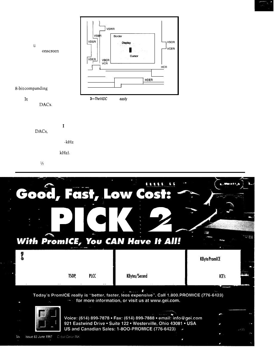
A program accessing mouse
data gets its information from
this buffer. If the read and write
pointers are equal, a call to read
the mouse buffer returns a -1.
The mo s e test program dis-
plays a cursor
that
follows the movements of the
mouse. If a mouse key is pressed,
the cursor leaves a colored line.
SOUND INTERFACE
The ARM7500 has an internal
DAC that can
be steered to left and right chan-
nels. also supports standard
Vertical Registers
HSWR
HBSR
HBER
HDSR
HCSR
Horizontal Registers
Figure
registers
relate to the video functions.
16-bit stereo
Some driv-
ers (e.g., the dual sound DMA chan-
nels) are the same for either choice.
When generating a 44.1
sample
rate, the clock to the DAC must be
The nature of the data stored is quite
different, however. Since chose exter-
-1.4112 MHz (32 x 44.1
Dividing
nal digital
the driver was writ-
32 MHz by 22 yields 1.455 MHz or 3%
ten to support this interface.
high (about a tone error).
The sound channel has dual DMA
pointers, enabling continuous sound
An LMC1982 between the DAC
data. Use Figure 4 to run the sound
DMA. When the diagram calls to Write
output and the input of the stereo
A, write the DMA-channel pointers
power amplifier controls volume and
SNDCURA and SNDENDA.
tone. It is programmed by sending a
serial bitstream with an open-drain
data line and a serial clock. Data
is then strobed into the device.
To operate the sound channel,
the sound frequency divider and
control registers are set up for
the sound type being played.
The sound DMA i rq routine is
installed, the buffers zeroed,
and the driver message queues
initialized.
Four sound buffers help keep
up with the sound DMA channel
and are initially loaded with
adjusted sound data. In the
diagnostic, the sound data is
8-bit data expanded to 32 bits.
Thus, it takes 1024 bytes of
input data to fill the playable buffer
with 4096. As each DMA buffer is
used up, the DMA loads a new buffer
address, setting the interrupt.
The interrupt routine also sets a flag
and updates pointers. When the last
buffer is loaded, the DMA overruns. To
reset the DMA int, the next DMA
channel is programmed. When all the
internal sound sample data is played,
control returns to the diagnostic.
Hi h performance memory emulation and
de ugging:
l
Stable and reliable on today’s embedded systems.
l
New faster access speeds now standard.
l
The best connection solutions for
PSOP and
chips.
l
Expanded Virtual UART support for industry-standard debuggers.
Ultra-Fast code downloads reduce
development time:
l
New high-speed download support for
Windows NT
l
90
over o PC parallel port.
l
Low-cost Ethernet support for UNIX systems.
New lower Prices for 1997:
l
128
now
just $495.
l
Source-level debugging systems
at a fraction of an
cost.
FLOPPY INTERFACE
The floppy attaches to a stan-
dard I/O Combo chip
663 or 665). It’s programmed
exactly as in a PC but at differ-
ent addresses. In particular, the
successive addresses are on word
boundaries, so and 16-bit
operations are supported.
Finished
(stop)
The ARM7500 has a special
chip select (COMBOCS at
Figure 4-The sound
has dual data pointers. The program interacts
with the hardware to maintain continuous sound
cal address
to select this
IDE INTERFACE
part as well as one that mimics the
The RC7500 sports two IDE
floppy DMA Acknowledge (CDACK at
tions-IDE1 connects to PC Combo
address 0x03012000).
and is located within its address space,
LOGICAL
‘tart programming devices today with the lowest cost and highest per-
formance CERTIFIED programmers. Enjoy a no hassle user interface for
ALL versions of Windows and DOS. Works with any PC of any speed
without a hitch. Device libraries added in less 2 hours to our Web cus-
tomer support section. Unique programming head options for gang pro-
gramming most microcontrollers and memory devices. Direct Docking
PLCC,
programming heads. Evaluate a unit today
with
satisfaction guaranteed
or
YOUR MONEY BACK!
(no penalties or restocking fees if unit is returned).
Call Today in USA 800-331-7766
303-733-6868 or Visit our Home Page:
w w
and a separate IDE2. Both have
separate address spaces for the
Western Digital Hard Disk reg-
ister set and the extra floppy
registers for the hard disk.
DOES THE SHOE FIT?
Obviously, this information
merely scratches the surface of
what the ARM7500 is all about.
If your application is along the
lines of an Internet appliance, medical
instrumentation (e.g., EKG display),
and GPS or airport display, the ‘7500 is
a chip you should check out.
Art Sobel is the hardware applications
manager of embedded products at VLSI
Technology. He has spent 24 years
designing disk-drive electronics and
controllers, laser interferometers and
printer controllers, many controller
chips, and speech synthesizers. You
may reach Art at
corn.
offer complete source code at
and
GNU cross-development software is
at
or
ARM7500
Sheet
RC7500, ARM7500
chips
VLSI Technology
18375 S. River Pkwy.
Tempe, AZ 85284
(602) 752-6630
Fax: (602) 752-6001
ARM7500 chips
Cirrus Logic, Inc.
3100 W. Warren Ave.
Fremont, CA 94538
(510) 623-8300
Fax: (510) 226-2180
www.cirrus.com/prodtech/
410
Very Useful
411 Moderately Useful
412
Not Useful
83
June 1997
Circuit Cellar INK@
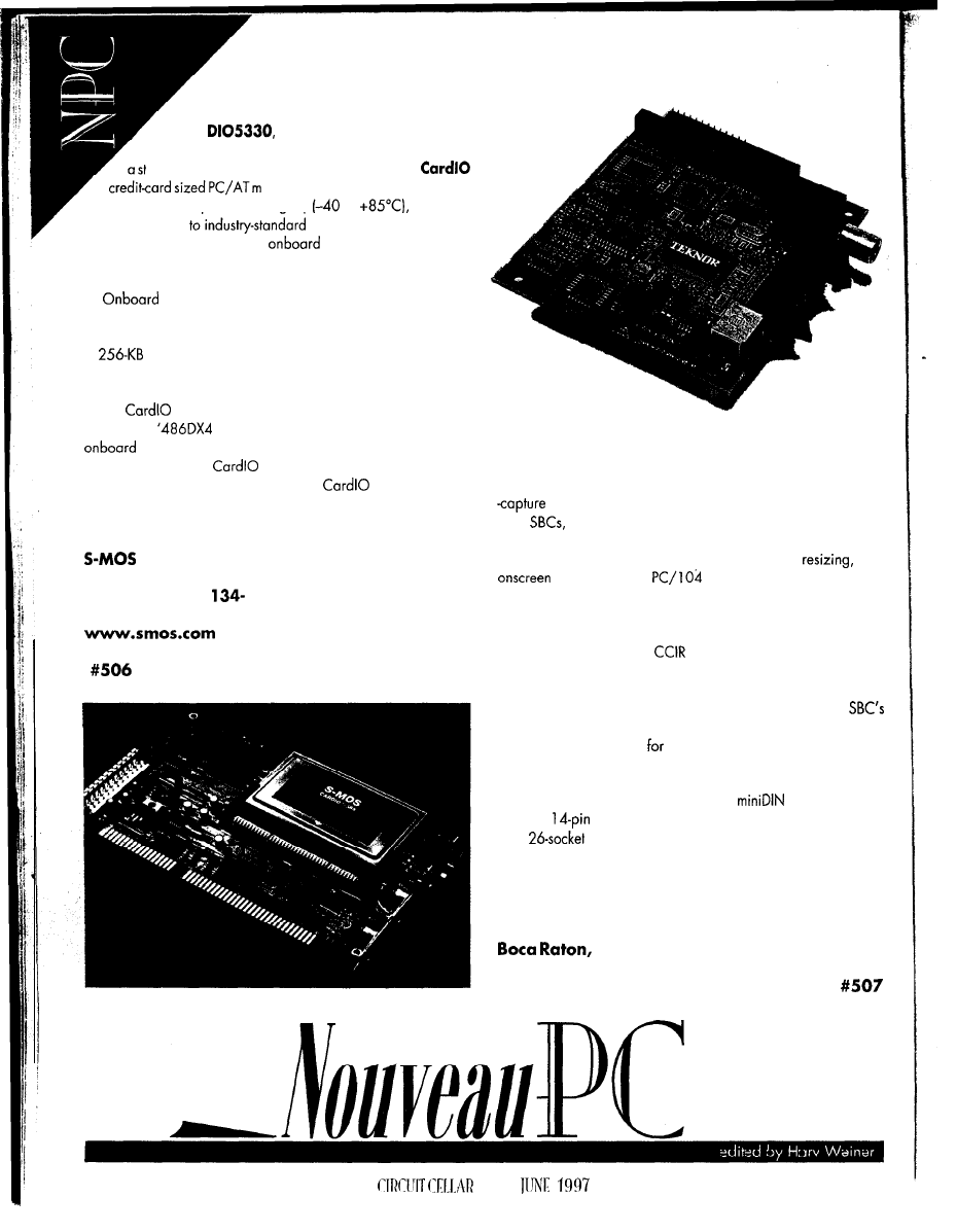
SINGLE-BOARD COMPUTER
The
an industrial computing board for
process- and motioncontrol applications, is available as
tond-alone board or powered by the company’s
otherboard. It offers operation at the
full industrial temperature range
to
a 4” x 7”
footprint, access
software (DOS or Windows
preinstalled, if requested) and
interfaces. Targeted em-
bedded applications include factory floor automation, hand-held
instruments, and test equipment.
features include serial and parallel ports, interfaces
for graphics, hard and floppy disk drives, as well as mouse and
keyboard controllers. It has up to 4-MB DRAM and resident BIOS
in
flash memory. Also included are an LCD interface with
backlight control circuitry, programmable watchdog timer, four
analog-input channels, and a power-management controller.
The
is a fully functional PC/AT motherboard, available
in ‘486 and
platforms with speeds up to 100 MHz and
memory of up to 16 MB.
The Dl05330 and
are sold separately. The Dl05330
sells for less than $300 in quantity. The
starts at $800 in
quantity. Pricing for
evaluation kits
starts at $300, depending
on components.
Systems
150 River Oaks Pkwy.
San Jose, CA 95
195 1
(408) 922-0200
l
Fax: (408) 922-0238
REAL-TIME VIDEO INTERFACE MODULE
The
VlPer Vision
TEK-380 interfaces automatically to vari-
ous video standards to accommodate noise-free video-display and
applications. Designed to complement the company’s
VlPer
the card features up to six composite or three S-video
inputs,
NTSC,
PAL, and SECAM compatibility, hue saturation,
brightness and contrast control, real-time image
and
positioning in a
form factor. Typical applica-
tions include automated shop floor equipment, surveillance sys-
tems, personal identification systems, in-vehicle readers and scan-
ners, and electronic kiosks.
Other features include
or square pixels for easier image
processing, linear zooming with interpolation for smoother edges,
full cropping control prior to capture, and the ability to save
captured images to disk. The card uses the VlPer industrial
internal video circuitry to produce full real-time video without
burdening the system bus
additional
bandwidth. Thus, the entire
system can run at maximum capacity at all times.
The VlPer Vision TEK-380 comes standard with one BNC
connector for composite video, one 4-pin
for S-video input,
and one
header to handle multiple inputs. Video output is
via a
header which interfaces to a VlPer industrial board.
Both standard and customdesigned software drivers are provided.
The unit sells for $395.
Teknor Industrial Computers, inc.
7900 Glades Rd.
FL 33434
(407) 883-6191
Fax: (407) 883-6690
40
INK
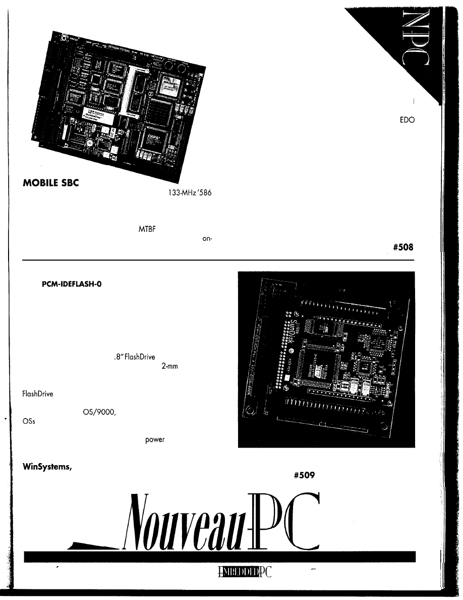
The PC-51 0 single-boord computer combines a
processor, six serial ports, a GPS interface, advanced video, and
48 lines of DIO on a 5.75” x 8” form-factor board. It is designed
for rugged mobile communications, data acquisition, and industrial
control applications, and it features an
of 13 years.
The PC-510 supports LCD and Et flat-panel displays, The
card 65550 video chip acts as a graphics accelerator to support
real-time video. Because the video circuitry oper-
ates on the Local bus at full processor speed, high-
performance programs like Windows execute very rap
idly. As well, 2 MB of video RAM is provided to accommo-
date a high-resolution display monitor. Power-management
functionality is also included. The board also includes a PC/l 04
interface, IEEE 1284 multifunctional parallel port, floppy- and
hard-drive interfaces, keyboard, speaker and mouse ports, watch-
dog timer, real-time clock, 2-MB flash disk, and 1 MB of
DRAM (expandable to 33 MB).
The PC-5 10 contains DOS 6.22 in ROM, as well as diagnostic
software to test and verify on-card I/O and memory functions. DOS
applications can be stored directly in the resident flash memory,
eliminating the need for a hard drive. The card also supports other
operating systems, such as Windows, Windows 95, Windows NT,
and QNX.
The PC-5 10 can operate either in stand-alone mode, or it can
be expanded via its PC/l 04 connector. The unit sells for $995 in
small quantities.
Octagon Systems
65 10 W. 91 st Ave.
l
Westminster, CO 80030
(303) 430-l 500
l
Fax: (303) 426-8 126
MASS-STORAGE MODULE
The
is designed for embedded systems requir-
ing low power, high shock and vibrational resistance, instant access to
data, and full compatibility with rotational disk
drives.
Its PC/l 04 form
factor provides up to 84 MB of formatted flash disk storage to replace
conventional disk drives in harsh environments. Applications include
program and data storage for data collection and logging, diagnostics,
process variables, and setpoints.
The board provides solid mechanical and electrical mounting,
permitting a user to install a 1
and cable it to a host
computer’s IDE interface. The drive plugs into a
connector and
fastens securely to the PC board. Since it appears as a standard IDE
interface, no special software drivers or utilities are required. The
products are 100% compatible with DOS, DOS applica-
tions, and other operating systems supporting IDE disk drives. It also
operates with QNX,
Lynx, and other real-time embedded
that interface to IDE drives.
The PCM-IDEFLASH-0 comes in an ADP-FLASH version if PC/l 04
stack mounting is not desired. It has a 4-pin
connector
rather than
PC/l 04 connectors. The PCM-IDEFLASH-0 sells for $50.
Inc.
l
715 Stadium Dr.
l
Arlington, TX 76011
(817) 274-7553
l
Fax: (817) 548-1358
l
www.winsystems.com
JUNE
1997
41
D S P B O A R D
The
Model
104
is designed for embedded applications
requiring the computational and I/O capabilities of a floating-point
DSP, as well as for DSP algorithm development. It can be operated as
a
PC/l
expansion board or a stand-alone unit, or it can be used
to control other boards vio the
04 b us in o system without a host CPU
board. This last mode permits the creation of a
embedded DSP
computerwith the unit performing functions normally
done
by the 80386
(or higher)CPU board. Th ese functions include the controlling of PC/l 04
video, RS-232 serial port, and analog I/O boards.
The unit is based on the Texas Instruments
floating-point
DSP operating at 50 MHz, for up to
performance. Included on the
board ore 256 KB of zero-wait-state SRAM, 5 12 KB of flash memory, digital I/O, and DSP
serial port expansion
.
A DSP software-development package containing an assembler, debugger, application examples, and
flash-memory programming utilities is included with the board. Price including software is $499 in small quantities.
Dalanco
l
89
Ave.
l
Rochester, NY 14618
(716) 473-3610
l
Fax: (716) 271-8380
l
Just
connect a
k e y b o a r d ,
a disk drive
your ready to run. Or
brget the drive and boot
from a Flash disk.
Modules for
.
SCSI, Ethernet,
for Point Of Sale and Wed
Browsers/Servers. Prices start at $200.00
Wide CPU Selection:
486DX. DX2, DX4. 586.
All
have Real Time Clock, Serial. Parallel, IDE, and Floppy.
On Board Watchdog Timer.
l
BIOS with Power Saving Green Mode.
Wide Bus Selection: PC/ 104, ISA. PCI.
10.4”
super
LCD Panel
l
Hardware and Cable kits included for most boards.
F a x
11 EMAC WAY, CARBONDALE, IL 62901
WORLD WIDE WEB:
DOS IN ROM!
5 7 5
1 4 4 m $ 1 5 0
5
$ 1 9 5
$95 EPROM
PROGRAMMER
Super Fast Programming
Easier to use than others
Does
NH
792
8088 SINGLE
BOARD
COMPUTER
4 2
CIRCUIT
INK JUNE 1997
An In-Depth
Look
at
Since
drivers are becoming more common, you need to know more
than
basics. After discussing
technology and algorithms,
shows us
how
interfaces to many storage devices.
n March 1996, the Personal Computer
Memory Card International Association
(PCMCIA) adopted a media-storage specifi-
cation called Flash Translation layer (FTL).
Although it was already an industry
standard, FTL picked up speed. The Minia-
ture Card Forum also recently proposed
this specification
standard
their
new small form-factor flash card. It’s becom-
ing the market’s most widely used and
supported flash file format.
The FTL specification defines the data
structures used to manage PC Cards and
Miniature Cards which have a linear array
of flash-memory chips. Algorithms imple-
menting the FTL enable flash to provide full
and transparent hard-disk emulation. So,
designers can provide solid-state
storage solutions that are lower cost than
cards based on
technology.
FTL-based drivers are being bundled
with more and more systems, ranging from
desktops and consumer products (e.g.,
digital cameras) to highly customized em-
bedded
In this article,
I
give you a
look into the FTL technology, its data
tures, and the algorithms implementing it.
H I S T O R Y
The FTL specification, based on
ogy patented in April 1995, describes a
virtual mapping system that enables
mon flash-memory components to provide
read/write capability.
With a block device driver interface, the
implementation of the algorithms that make
up this mapping scheme lets any
memory-based storage device fully
late a hard drive’s functionality. The
tion is transparent to the host computer’s
native OS and file system. Using these
algorithms, the flash storage medium
comes a flash disk.
DOS Sector Number
Figure Contiguous sectors are mapped
physical locations on the medium. The
keeps track of their locations via a map
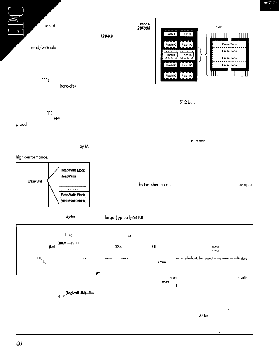
The fact that FTL can
use the native OS’s file
system makes this solution
stand out from all others. Also,
it’s significant that FTL implements a
fully
disk.
Many programs let you use a flash
.
memory array as a Write Once Read Many
(WORM) device. But, they require special
utilities to update the disk image, which is
usually a slow process.
Microsoft’s
and II drivers were an
early attempt to provide
emula-
tion. But, these solutions replace the stan-
dard file system that’s part of the OS. So,
standard OS disk management and diag-
nostic utilities can’t be used on a flash disk
managed by an
driver.
In addition, the
II
linked-list ap
is plagued with performance and
reliability problems. The medium is easily
corrupted by power failures or other events
that interrupt a write cycle.
The FTL specification, coauthored
Systems and SCM, provides a uniform,
and robust solution for
Figure 2: Erase units are com-
posed of individual erase
For example, two Intel
chips connected in parallel yield
a
erase unit.
working with flash PC Cards.
The IP rights associated with
the patent granted to M-Sys-
tems were released into the
public domain for designs us-
ing linear-flash PC Cards and
Miniature Cards. A variety of
companies and user groups can therefore
provide their own FTL implementations.
Flash Memory Card
Interleaved Flash Devices
Odd
Addresses
Addresses
complicating data updates. The blocks are
much larger than the units of data (usually
sectors) stored on the medium.
WORKING WITH FLASH MEMORY
Flash memory offers some attractive
features for mass data storage. They are
nonvolatile-the data is retained indefi-
nitely without any power to the flash com-
ponents. No back-up batteriesare needed.
Unless handled properly, this problem
complicates data updates. Larger blocks of
unrelated data must be rewritten to update
a single sector.
LIMITATIONS OF FLASH
Erase Unit
Erase Unit
Erase Unit
Black
. . . . . .
Flash is low cost compared to other
battery-backed solid-state solutions. It con-
sumes low power and takes up little space,
so it’s ideal for mobile and hand-held appli-
cations. Also, it’s solid state, so it can work
in harsh, rugged environments where me-
chanical disks are unsuitable.
The
of
times flash can be written
and erased is limited and depends on the
specific
flash
technology. Typically, it’sabout
1 million times per block.
Managing data on flash memory is
complicated, however,
straints of the flash technology-most im-
portantly, the nonrewritabilityofdata. With
flash, you can’t write over existing data
without a slow erase cycle.
In many flash components, erase blocks
A region of flash close to its cycling limit
usually displays sporadic write failures that
become more frequent. Eventually, the sec-
tor is no longer erasable or writable.
Flash cells can be accidentally
grammed or overerased by incorrect pro-
gramming. When this occurs, the flash
usually won’t respond to programming for
a period of time or it responds very slowly.
This condition can usually be reversed, but
Figure 3: Each erase unit is dividedinto evenly
sized blocks, each about 5 12
long.
are
blocks), further
the cell’s life is shortened.
FTL Definitions
Block-This sector-sized (5 12
unit of data stores information, control
data, on the medium. It is a subdivision of an erase unit.
Block Allocation Map
control structure stores Block Alloca-
tion Information
about blocks on the medium. It includes a
entry
for each block on the medium.
Erab Unit (EU)-This area of the flash medium is handled as a single erasable
unit by
although it may contain one
more erase
This
is
determined
the hardware configuration of the flash and is identified during
media formatting.
Erase Unit Header (EUH)-This header contains information specific to the
erase unit and global information about the entire
partition.
Erase Zone-This area of flash must be erased as a single unit due to the
characteristics of the flash chip.
logical Address-This address is based on accessing the medium in logical
Erase Unit order.
logical Erase Unit Number
logical number is assigned
to an erase unit by the
assigns logical numbers to erase units in order
to remap the ordering of the physical medium and simplify recovering
superseded areas.
Partition-This region of the flash medium is dedicated for a specific use. The
medium can contain a partition at the beginning that contains binary
information, an FTL-handled partition located afterthefirstpartition, and a final
partition for storing additional binary information. Once the medium is
formatted, the physical starting address of each partition remains fixed.
Physical Address-This address is based on accessing the medium in Physical
Erase Unit order [i.e., the hardware address of a location in the flash array).
Physical Erase Unit Number (PhysicalEUN)-This number is given to an
erase unit based on its location on the physical medium. This unchanging
number is implied by the erase unit’s position. The erase unit at the beginning
of an
partition is known
OS
the first physical
unit. If the partition
begins at physical address zero, the first physical
unit is number zero.
Reclaim-Also known as garbage collection, this procedure recovers blocks that
weredeleted orcontain
within the
unit being reclaimed.
Read/Write Block-see Block.
Replacement Page-This alternate VBM page contains entries that override
the values in the original VBM being replaced.
Transfer Unit-This
unit is reserved for storing read/write blocks
data from an
unit being reclaimed. Transfer units are not included in the
formatted size of the
partition presented to the host file system.
Virtual Address-This address is recorded in a read/write block’s allocation
information (BAI), representing where the stored data appears in the virtual
image presented to the host system. It is calculated by multiplying the virtual
block number (e.g., the sector number] by the block size (5 12 bytes).
Virtual Block-This unit of information is used by the host file system above FTL
for reading and writing data to the medium. It’s usually called sector when
dealing with file systems,
Virtual Block Map (VBM)-This array of
entries maps a virtual block
number to a logical address on the medium.
Virtual Page Map (VPM)-This structure maps the locations of VBM pages.
It is never stored on the medium. Instead, it is stored in the host’s system
memory and rebuilt every time a new card is inserted power is cycled.
CIRCUIT CELLAR INK JUNE 1997
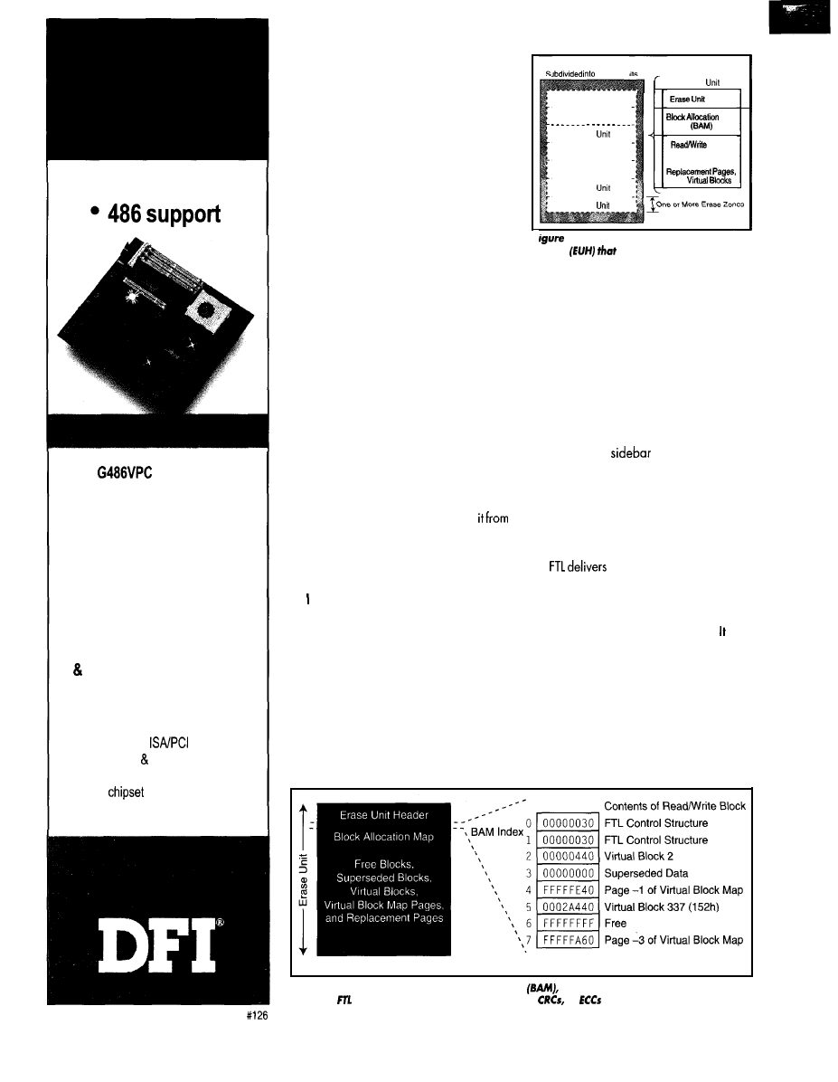
. 7 ISA slots
The
motherboard
combines quality and
affordability with an industrial
design to meet your needs.
Seven full length ISA slots
ensure expandability for the
cards that you use.
Our engineering staff will
gladly discuss custom
motherboard designs. FCC
UL certified systems are
also available.
l
Six full length l&bit ISA, One
shared 8-bit
slot
l
Intel, AMD SGS-Thomson
486 CPU support
l
VIA
l
Up to 64MB RAM, 256KB cache
F L A S H I S C O M P L I C A T E D
Because of the nonrewritability of flash,
data must be organized via flash file sys-
tems. Damaging or corrupting the data
(i.e., the low-level format) may mean user
data can no longer be accessed.
Since an accidental or deliberate power
failure, often due to prematurely removing
the flash card, is possible anytime, writing
to the flash must be done in a way that
ensures no loss of existing data.
Even if no flash-hardware errors occur,
the data and recording format must be
coherent at all stages of writing. Also, manu-
facturers use incompatible programming
algorithms to control the flash.
FLASH FILE
SYSTEM FUNCTION
A flash file system is a software driver
that makes flash memory emulate a disk
drive. It lets the developer use a common,
well-understood mechanism to store data
on a nonvolatile solid-state medium. The
resulting flash disks may be interchanged
with mechanical disk drives, adding flex-
ibility to the design and debug process.
A well-written flash file system emulates
a disk so transparently that the user and
systemcannotfunctionallydistinguish
a mechanical disk drive. However, it must
perform low-level operations to accomplish
this as well as overcome the constraints of
flash components.
examine these operations in detail, but
these features include:
l
mapping OS model (disk sectors) to
physical model (flash blocks) as in Fig-
ure 1
endurance
l
managing the mapping tables
l
maintaining flash erase operations in the
background to optimize performance
l
wear-leveling for increased flash-media
Flash Memory
Erase Un
Erase Unit
Erase Unit
Erase
Erase Unit
Erase Unit
Erase
Erase
Erase
Header
Map
Blocks
Used for
Virtual Map Pages.
and
4:
Each erase unit has an emse-unit
header
contains information about
the specific unit as well as information about
the entire medium.
l
detecting errors for mapping bad or
worn-out flash blocks
l
protecting existing data and directory
structures for reliability
l
implementing different programming al-
gorithms for specific flash components
Before getting into the structure of the
FTL data, look at some terms of the specifi-
cation (see the
“FTL Definitions”).
FTL DATA STRUCTURES
An OS file system (not a flash file system)
randomly updates any
block
on the system’s
storage medium. But, unless flash is in its
erased state, it cannot accept new data.
thiscapabilityto higher level
software layers by remapping requests to
write blocks to unallocated or free areas of
the medium and invalidating the area that
previously contained the block’s data. also
records where the remapped block is placed
for subsequent read accesses.
emulate the standard hard-disk sector size.
In effect, FTL presents a virtual-block
storage device to the higher level software
layers. Virtual block size can be deter-
mined when the storage medium is format-
ted, but it’s normally set to 5 12 bytes to
A Portion of the Block Allocation Mao
Figure 5: In this particular block allocation map
the read/write block size is 5 12 bytes.
A/so, the
partition does not store checksums,
or
for the virtual-block data.
48
CIRCUIT CELLAR INK JUNE
1997
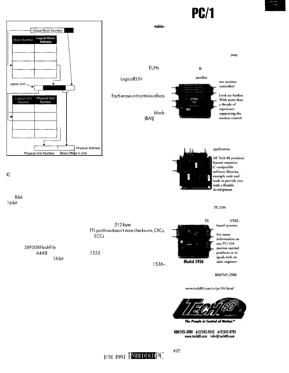
The
04
Motion Control
Experts
Block Offset
Virtual Address
Figure 6:
The mapping functions
can be defined as a set
of
lookup functions based on the
number
of
the sector that the
operating system wants to access.
Block Offset
Carried Forward
information about the state of the
entire flash medium. All
on
the medium are identical except
for their
field values.
Logical Address
Depending on its technology, each flash
on a PC Card is divided into one or more
erase zones of equal size. Each erase zone
is the minimum contiguous area that can be
erased in a single operation.
If
devices are interleaved to provide
storage, the corresponding physical
zones on two adjacent devices combine as
a single erase zone. One device gives even
addresses, and the other, the odd ones.
An erase unit is a multiple of one or more
contiguous erase zones. Its size is set when
the medium is formatted (see Figure 2).
For example, if the flash components
are Intel
chips, every
chip has sixteen
erase zones. If two
chips are connected on a
data bus,
the erase-unit size is 128 KB.
T R A C K I N G T H E B L O C K S
tion data for the unit’s read/write
blocks.
For
each
read/write block,
a four-byte value (i.e., the
allocation information
tracks
the block’s current state.
A read/write block in an erase
unit can be in only one of four
states-free, deleted, bad, or allo-
cated. It can also have one of four
types of information-FTL control
structures, virtual-block data, vir-
tual-block map pages, or replacement pages.
The encoded BAI tracks the block’s con-
tent and its state. The block allocation map
(BAM) is normally stored immediately after
the EUH. Some flash contains hidden areas
that store this data instead of using main
storage space. The type of storage area,
main or hidden, is defined in the EUH.
Figure 5 shows the contents of a BAM.
Each map entry describes the contents of a
corresponding read/write block. This ex-
ample uses a
block size, and the
or
for virtual-block data.
The first two read/write blocks store the
EUH and BAM. The third (bytes 1024-
of the erase unit) holds data for the
third virtual block used by higher level soft-
ware layers. The next block (bytes
2047) holds superseded data, and the block
following it has a virtual-block map page.
1
ERASE ZONES
A N D
U N I T S
E R A S E - U N I T H E A D E R
FTL divides every erase unit into one or
more equally sized read/write blocks (see
Figure 3). Each read/write block is the
same size as a virtual block (or DOS data
sector) used by the host file system.
As shown in Figure 4, each erase unit
contains an erase unit header (EUH) nor-
mally located at the beginning of the erase
unit (i.e., offset zero). However, it can be
mapped to a different offset.
The EUH contains specific information
about its erase unit as well as global
V I R T U A L - B L O C K M A P
The BAM tables carry enough informa-
tion for the FTL algorithm to track the virtual
blocks and control structures on the me-
dium. However, the algorithm required to
track the locations would be slow since it
would rescan the entire medium every time
it looked for the location of a virtual block.
Instead, FTL incorporates an additional
map on the medium called the virtual-block
map (VBM). The VBM comprises an array
N
eed motion control within
PC1104 application?
Overwhelmed by the number of
products vendors out there? Looking
for a motion control specialist instead
of just
PC/ 104 vendor with
Model 5912
Encoder Interface
needs of OEM
customers, Tech
80’s family of
PC1104 modules can meet the encoder
interfacing and servo &stepper control
demands of your embedded
Model 5928
environment.
Servo Controller
AND if your needs
extend beyond the
realm, Tech
80 has the industry’s most extensive
line of board-level motion control
products for PC, STD and
Stepper Controller
regarding your
current
project,
please contact us at
or
visit us at:
Minneapolis, Minnesota USA
l
l
(fax)
l
49
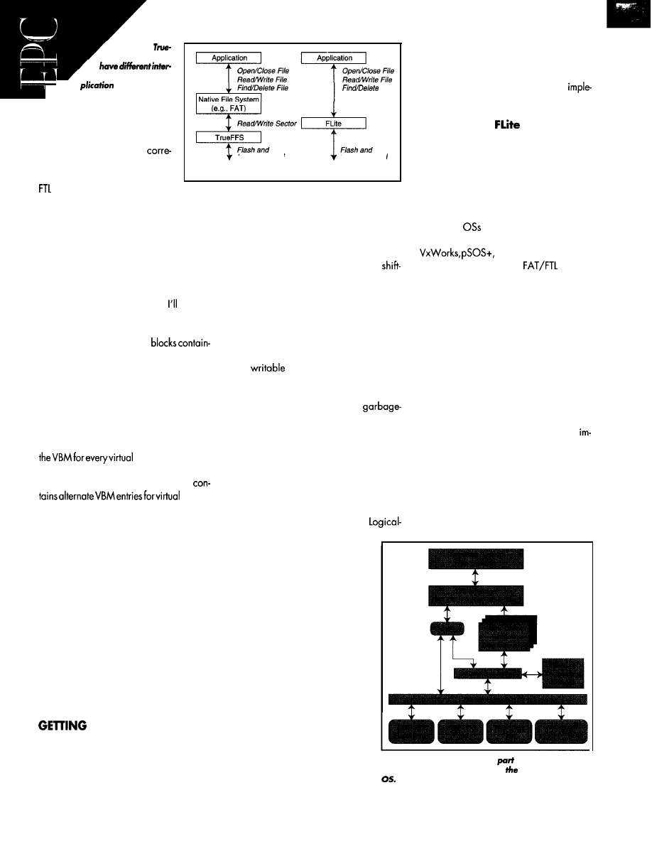
Figure 7:
FFS and FLite
faces with their ap-
but maintain
the same low-level func-
tionality.
t
of four-byte entries, each
sponding to a virtual block and
containing its logical address.
uses the virtual-block number
from the host as an index into the VBM.
As virtual blocks get assigned to physi-
cal blocks, the appropriate entry updates
in the VBM, which is on the medium. So,
when an entry is updated to show it has
moved, the physical block containing the
VBM needs to be changed, too. This situa-
tion would become a performance issue if
it wasn’t addressed properly, as discuss.
The VBM storage space is allocated
when the medium is formatted. A mecha-
nism differentiates between
ing data and those holding VBM pages.
Blocks with VBM information are treated as
virtual blocks with negative numbers, while
virtual blocks have positive numbers.
R E P L A C E M E N T P A G E
Replacement pages solve any perfor-
mance degradation caused by updating
block thatchanges
physical location on the medium. As its
name implies, a replacement page
blocks.
V I R T U A L P A G E M A P
The virtual page map (VPM), the last
map generated by FTL, is never held on the
medium. Instead, it is reconstructed from the
VBM contents, which are always on the
medium, every time the system is powered
up or a new card is inserted.
Each entry in the VPM tracks the loca-
tion of the appropriate VBM page. Since
the VBM is stored on the medium, these
pages move around as they are updated.
The VPM provides the entry point into
the VBM. Without the VPM, every access to
the medium requires a complete media
scan to find the appropriate VBM.
A P H Y S I C A L A D D R E S S
Figure 6 shows how a virtual-block num-
ber gets translated into a physical address
with the required data. It shows some of the
key features of the FTL algorithm. All virtual
50
File
Socket Control
Flash Media
Socket Control
Flash Media
blocks need the same number of address
translations to get to the physical address
(i.e., accessing two translation maps).
Because of pointer arithmetic and struc-
tures sized as powers of two, the arithmetic
involves very fast simple shift-left and
right operations. information in the maps
can always be reconstructed from redun-
dant information on the medium.
TrueFFS is a driver intended for an OS
with an existing file system. It typically
comes in a binary format compatible with
the specific OS and is available for many
standard
(e.g., DOS, Windows 3.x,
Windows 95, Windows CE, QNX,
etc.).
FLite, which stands for
Lite, is a
version of TrueFFS targeted to applications
with no built-in file system (i.e., they need a
file system and the FTL data format). It’s
customizableand provided with sourcecode.
RECLAIMING UNITS AND BLOCKS
Theabilityto reclaim superseded blocks
enables FTL to provide a solution that works
as a
disk. When the medium is
formatted, atleastoneeraseunitissetaside
(i.e., a transfer unit). When the medium no
longer has any free blocks, a
collection cycle is executed.
FLite includes DOS
FAT
file
functions, so
an application lacking native file-system
capability can write files directly to the
flash media in a DOS-compatible file for-
mat. The combination of DOS FAT file and
FTL compatibility ensures easy data inter-
change between a personal PC and an
embedded system.
The transfer unit is always held in an
erased state, ready to receive data. During
this cycle, the medium is scanned for an
erase unit that has garbage blocks.
When a unit is found, blocks with good
data are transferred to the transfer unit. To
show that it now contains valid data, the
transfer unit’s EUH is updated. The
EUN field from the unit that had the
garbage data is copied and placed
in the transfer unit’s EUH.
This capability may be particularly
portantwhen using removable flash media
(e.g., PC Cards and Miniature Cards).
Both FLite and TrueFFS use the same FTL
algorithms and technology.
Where does TrueFFS fit into the system?
TrueFFS and FLite are generally used as
block device drivers which sit under the
Once the data is in the transfer
unit, the old unit is erased and it
becomes the new transfer unit.
When data was copied into the
transfer unit, the blocks containing
garbage data were not copied.
Thus, when it becomes a new unit, it
has blocks free to accept new data.
I M P L E M E N T A T I O N
FTL is a specification for a set of
data structures that provides a mech-
anism for tracking the location of
data on flash media. However, this
specification doesn’t address all the
implementation issues involved in
providing a fully functional driver
Figure 8: The TrueFFS driver is
of a sotiware stack
that provides a data path from
flash media to the
that can provide a robust solution that
interfaces with an OS or application.
Let’s look at TrueFFS and FLite, which
have been recognized as the leading
mentations of the FTL specification.
T r u e F F S A N D
M-Systems has two different forms of FTL
available to developers for use with flash
memory components or cards.
CIRCUIT CELLAR INK JUNE 1997
Sets The Pace
In
Data Acquisition
Scan 16 Channels...
Any Sequence...
500
Analog
Module
with Channel-Gain Table and FIFO
With Companion
133 MHz
PC/l 04
The
offers
versatile embedded functionality
Our
and ISA Bus
Product Lines Feature
Intelligent DAS Cards With
Embedded PC and DSP,
Analog and Digital
CPU,
Shared Memory,
SVGA, PCMCIA,
CAN
Bus and GPS Modules
State College, PA 16804-0906 USA
234-8087
URL:www.rtdusa.com
Scandinavia Oy
Helsinki, Finland
Fax: 358-9-346-4539
RTD is a founder of the
Consortium
52
native
file system of the OS (see Figure 7).
In thecaseof Ftite,
not beanyfile
system. So, Ftite optionally provides one.
Block device drivers provide:
l
compatibility with many file systems
l
transparency in operation
l
compatibility
with
all file and disk utilities
for the OS
l
compactness
In Figure 8, you see how TrueFFS fits
into an OS structure. It may interface to a
number of different flash storage devices.
These may be removable flash cards,
an
resident flash array, or a
separate flash-disk board (e.g., ISA- or
PC/l O&bus boards). In any
case,
TrueFFS
remains unchanged, and the specific inter-
face is dealt with in a socket-services layer
under TrueFFS.
In some cases, a Card Services Software
manager arbitrates the socket’s operation.
This often happens when a system has
multiple cards (e.g., flash, modems, LAN,
etc.), and a specific version of TrueFFS is
necessary.
TrueFFS includesstandard
drivers
for common flash
devices used for flash-disk applications.
Although these include devices from Intel,
AMD, and
and their compatible
devices, there may be a need to add more
external
to support other devices.
External
are usually added as
plug-in drivers via a standard interface to
the Card Services layer of the software.
With Ftite, the
are more often added
via source code and then implemented as
a single monolithic driver.
REFINED ENOUGH?
FTL
robust, industry-standard, proven
flash data format standard that has been
widely used and adopted. It fully emulates
a hard disk, making flash easy to read and
cost, low-power, rugged, reliable storage
medium of choice for hand-held, portable,
embedded computer applications. It’s be-
a n d i s a v a i l -
able from third-party suppliers for all other
platforms.
TrueFFS and Ftite are the leading imple-
mentations of FTL. They both incorporate
the FTC data format standard to ensure
interoperability across diverse platforms.
INK
1997
Over the past six years, they have been
refined in different operating architectures
books,
ity, and flexibility of a
Raz Dan is the customer
e n g i n e e r i n g m a n -
ager for M-Systems. He is currently respon-
s
i
b
l
e
for custom applications, advanced
technical support, and system integration
for the company’s product
R
a
z
h
o
l
d
s
a BSEE from Tel-Aviv University. You may
reach him at
SOURCES
FTL Specification, PC Card Standard, Media
Storage Formats Specification
PCMCIA
2635 N.
1st St.
San Jose, CA
95 134
(408) 433.2273
Fox: (408) 433.9558
TrueFFS,
M-Systems, Inc.
4655
Old
Ironsides Dr.
Santa Clara, CA 95054
( 4 0 8 ) 6 5 4 - 5 8 2 0
Fax: (408) 654-9 107
and up)
SCM Microsystems, Inc.
13 1
Way
Los Gotos, CA 95030
( 4 0 8 ) 3 7 0 . 4 8 8 8
Fax: (408) 370.4880
Inc.
2 Vision Dr.
Natick, MA 01760
(508) 65 l-0088
Fax: (508) 65 l-8 188
Phoenix Technologies ltd.
2575 McCabe
Irvine, CA 92714
(7 14) 440-8000
Fax: (714) 440.8300
TrueFFS
1
1838
Plaza Ct.
San Diego, CA 92
14
( 6 1 9 ) 6 7 3 . 0 8 7 0
Fax: (619) 673-l 432
413 Very Useful
4 14 Moderately Useful
4 15 Not Useful
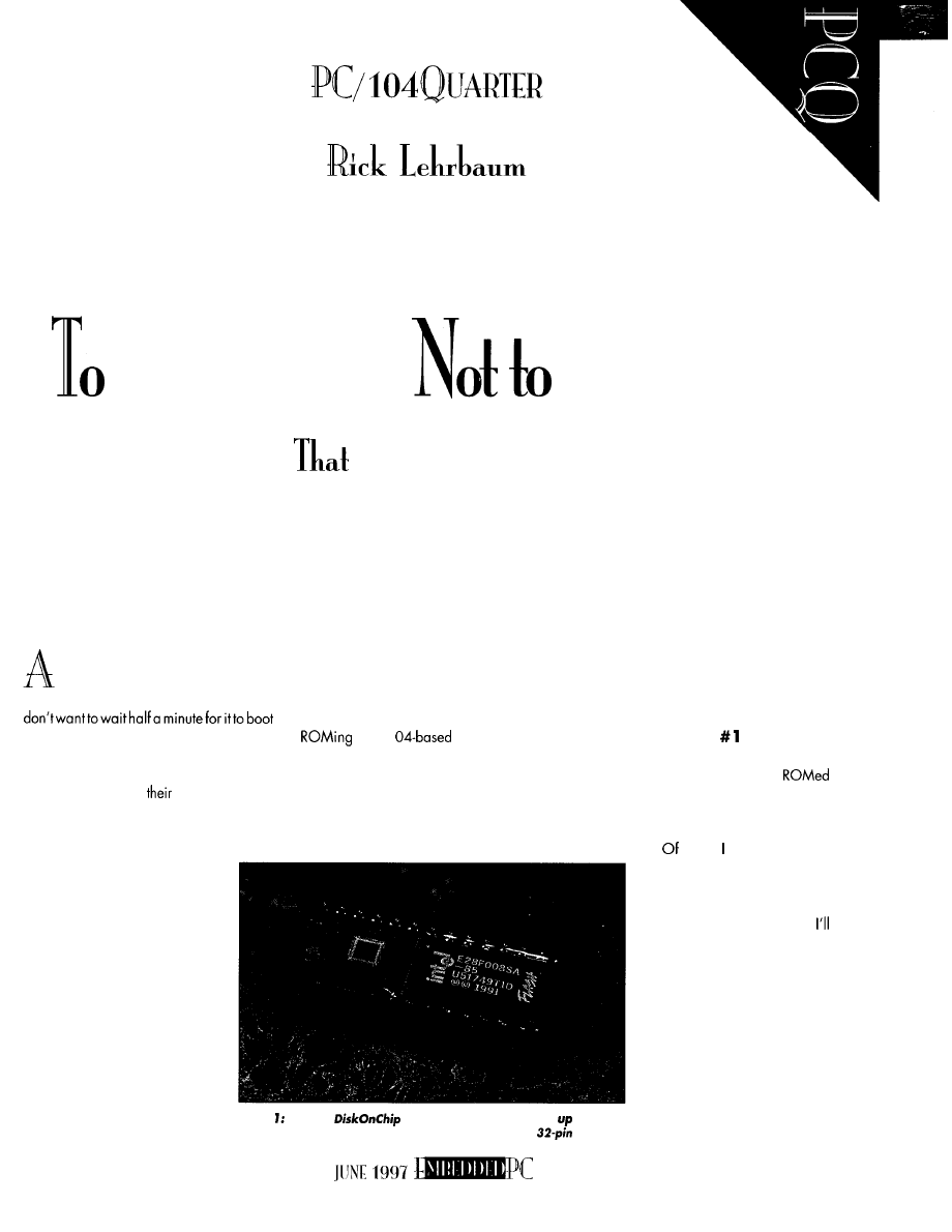
ROM
or
ROM
is
the
Question
We all take for granted the three minutes of boot-up time for desktop computers.
But, we’d never tolerate such performance in a task-specific system. Rick looks
at ways to gain instant response from
an
embedded
PC/7 04
computer.
n embedded system should operate
like an appliance. When you turn it on, you
its operating software from a hard disk
drive. It has to perform its function instantly.
application rather than operating it out of
a disk drive.
a PC/l 04 application. Fooled ya! Here’s
my pitch....
Such systems, if they contain microcom-
puters, normally load
software instantly
from ROM (or EPROM), not disk drives.
There are other reasons why you may
not want an embedded system to
use a conventional disk drive. In
applications with critical data-in-
tegrity requirements, “soft” read/
write errors are unacceptable.
You’re probably set to hear all about
a PC/l
application. Do
you expect “Rick’s tips” on splitting software
into independent code and data blocks
that go in separate ROM and RAM devices?
Well, this month, my mission is to make
the case
why
you
really don’twant to ROM
And, disk drives don’t work
over wide temperature ranges, so
they’re usually limited to indoor,
temperature-controlled environ-
ments. Shock and vibration are
also problems. Size, power con-
sumption, and heat generation
can also be reasons to avoid disk
drives in embedded systems.
So, it may seem like a good
idea to ROM your embedded-PC
KEEP AN EYE ON
You
may have used microcontrollers on
other projects, and you probably
your application. But, just because that’s
how it’s done on a microcontroller doesn’t
mean it’stherightwayforanembedded PC.
course,
assume you want
to harness the full potential of PC
compatibility. While I’m sure you
have a whole slew of reasons
for using an embedded PC,
bet software tops your list.
Wanttosimplifyandenhance
your embedded project through
the vast storehouse of PC OS,
driver, and development soft-
ware? If so, remember: to reap
the benefits of PC compatibility,
stay PC compatible!
The PC was designed as a
disk operating system (DOS)
machine. PC software is always
Photo The tiny
from M-Systems squeezes to
12 MB of f/ash memory into the same package as a
EPROM.
53
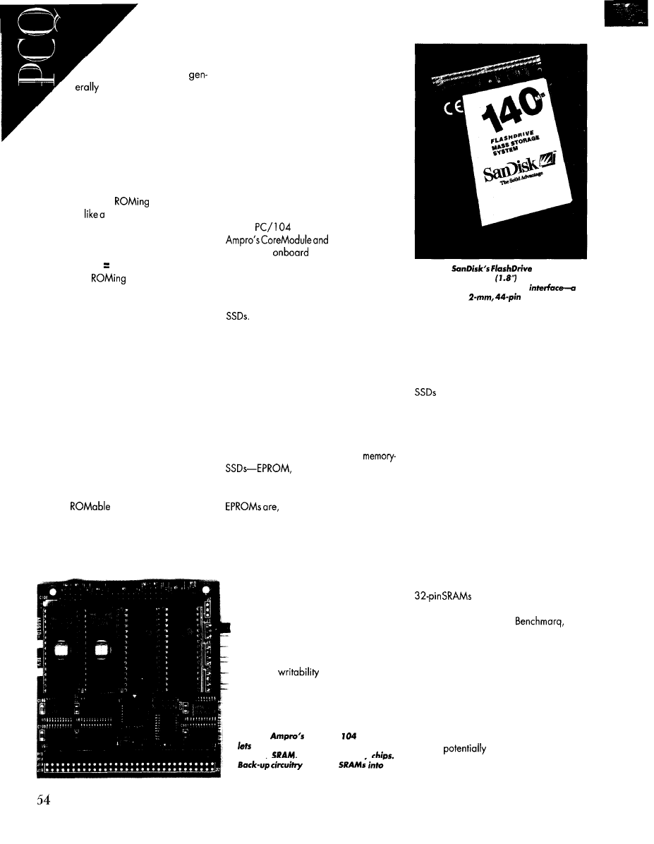
into system DRAM, where
it runs. (Even the BIOS is
“shadowed” in DRAM for
faster execution.)
So, if you ROM your embedded
application (and perhaps even DOS), you
abandon the PC “standard.” Don’t be
transferred from disk
surprised when you lose access to tons of
off-the-shelf device drivers, function librar-
ies, and application programs that rely on
a DOS environment.
If you insist on
your PC/l 04
application
microcontroller, be ready
for the traditional microcontroller develop-
ment headaches and limitations.
EMULATION FLATTERY?
Instead of
the application, use
a solid state disk (SSD), which “emulates”
normal disk drives.
With SSD, a software driver transforms
accesses to a normal disk drive into ac-
cesses to some form of memory. It’s like a
RAM disk, except that an SSD is typically
used as a boot drive.
Since nearly every PC program makes
disk accesses via DOS or BIOS functions,
the system can’t tell the difference between
the SSD and a real disk drive. Therefore,
SSD-based embedded-system development
doesn’t require special expertise, as long
as you take advantage of one of the readily
available forms of plug-and-play SSD.
You can develop your application on a
PC with normal disk drives. You don’t need
to write
code. You don’t even
have to know how DOS organizes or uses
the PC’s memory space!
Simply develop and test your applica-
tion using your favorite OS, programming
language, and other software tools just like
it’s going to run on a conventional disk
drive. Once you’re satisfied, transfer the
application to the SSD.
This procedure depends on what type
of SSD you’re using, but it’s normally fast
and easy. After transferring the application,
remove the normal drive and reboot.
The system should boot and run from
SSD. That’s it! SSD converts “software” to
“firmware” instantly and painlessly.
MAKING AN SSD
There are quite a few SSD approaches.
Many
embedded PCs (e.g.,
little Board prod-
ucts) have
sockets built into the
BIOS where you can plug in SSD devices
and driver support to emulate a bootable
A: or C: drive.
You can also use PCMCIA cards as
Some SSD drives look and act like
ordinary IDE or SCSI
disk
drives,
but they’re
based on nonvolatile memory, not magnetic
media.
In general, you need a nonvolatile mem-
ory device and an appropriate SSD soft-
ware driver. Before examining some of the
SSD options available, let’s review current
technologies and interface architectures.
TECHNOLOGY OPTIONS
There are three main choices of
device technology for
N V R A M , a n d f l a s h .
A s a n S S D t e c h n o l o g y , E P R O M h a s
serious limitations.
o f c o u r s e ,
usable only as read-only SSD drives. They
can’t help you write data into an SSD
during system operation.
Since EPROMs generally can’t be erased
and reprogrammed while they’re
plugged into the target embedded PC,
you have to program them beforehand.
Obviously, it’s a nuisance (and, some-
times, expensive) to update an embed-
ded system’s software in the field.
On the other hand, the per-unit cost
of EPROM SSD can’t be beat. So, when
in-system
isn’t required and
cost is critical, an EPROM-based SSD
may be just the ticket.
photo 3:
SSD PC/
module
you mix-and match your choice of
EPROM,
and flash-memory
converts
NVRAM.
Photo 2:
looks and
acts like a miniature
IDE hard disk, so
it’s easy to use. Note the IDE
high-density,
connector.
Using nonvolatile RAM (NVRAM) as an
SSD is probably the easiest approach. it’s
simple, requiring one or more RAM chips
(usually 32-pin DIP), a nonvolatile control-
ler, and a back-up battery.
Since they’re fully read-write, NVRAM
can be programmed directly within
the target embedded PC and used like
ordinary read-write disk drives (provided
‘you have the right SSD driver software).
If you design NVRAM sockets directly
into your application, you have to deal
with making an SRAM nonvolatile. You
can buy the necessary logic in a single tiny
chip, add a battery, and hook it up.
Don’t underestimate the technology in
that little chip! It’s critical that the SRAM be
protected from accidental write strobes
during system power cycles and that its
power be properly switched to and from
the back-up battery at the right time.
It’s easier to get NVRAM from special
with built-in back-up batter-
ies and control logic. They’re available from
Dallas Semiconductor,
and
others. Onecompanyevenmakesadevice
with a replaceable, snap-on battery.
While NVRAM has the advantage of
read-write simplicity, it has a couple of
disadvantages. One is cost. SRAM is the
most expensive form of memory and can
be many times as expensive as EPROM.
Another problem is temperature. Batter-
ies have a limited operating temperature
range,
excluding
an embedded
PC’s NVRAM SSD from certain applica-
tions. And, there are environments where
CIRCUIT CELLAR INK JUNE 1997
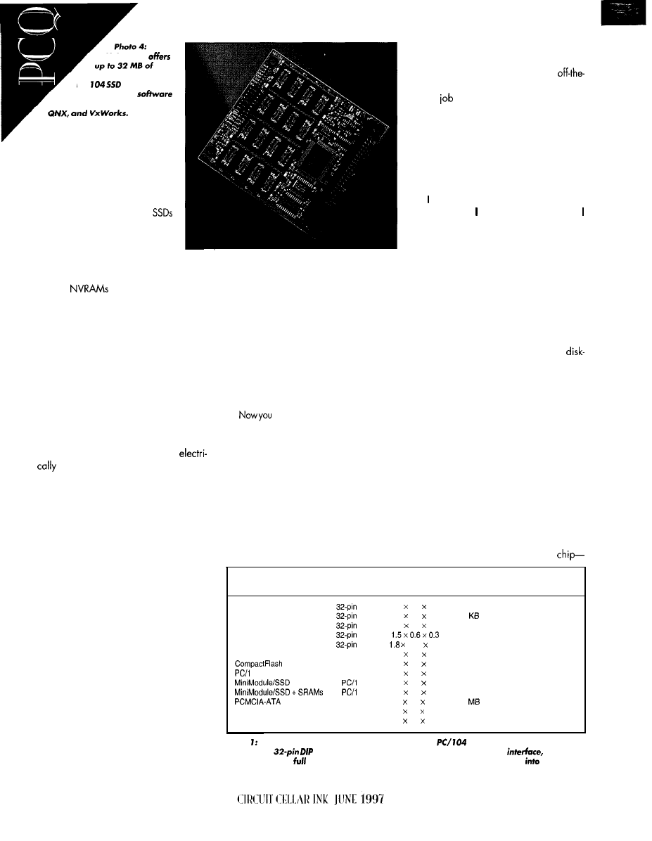
M-Systems
flash memory on this
PC/
module. The
product’s support
works
with DOS, Windows,
batteries aren’t allowed due to
their corrosive (sometimes explo-
sive) chemicals.
Of course, batteries don’t last
forever. Systems with NVRAM
eventually need their batteries re-
placed, which can be inconvenient
and costly. It also means expen-
sive system down time and loss of valuable
data.
So, if
have all these problems
and EPROMs are read-only, can any other
memory technology work well as an SSD?
That brings us to..
FLASH MEMORY
Flash is closely related to EPROM. But,
some clever semiconductor scientists fig-
ured out how to use quantum effects to
make an EPROM that can be erased and
reprogrammed electrically.
“isn’t that an EEPROM?” you might ask.
Not exactly.
EEPROM was the first form of
erasable/programmable
ROM. But it
was more expensive than SRAM! Flash is
only slightly more expensive than EPROM.
Unfortunately, flash isn’taseasytoerase
and reprogram as SRAM. But given its low
cost, so what if it takes a little extra effort!
Flash-device erasing and programming
requirecareful attention todetails. Data and
write control signals must sequence just
right or the data neither records nor pro-
grams fully into the memory cells.
Also, flash wears out. It only lasts a
specified number of erase/write cycles.
Fortunately, it’s rated for hundreds of thou-
sands of cycles, and there are ways to
manage its lifecycle.
One method is to reread the data after
writing to a flash location to verify that it
was written successfully. As the location
wears out, you might need to write the data
several times to get it to program success-
fully. Eventually, it fails completely, but it
does extend the life of flash for a while.
If a flash device needs to be written
many times, it’s critical that the writes be
56
evenly distributed or it may wear out pre-
maturely. It’s like rotating your car tires. This
process--called “wear leveling”-is a criti-
cal function of flash support software.
As if this wasn’t enough, flash doesn’t
let you rewrite a single location. You must
erase and rewrite some minimum block
size. Blocksize has been steadily shrinking
as flash technology evolves, so it’s disap-
pearing as a key issue. But, it used to be an
entire chip, which caused some interesting
SSD implementation challenges.
track”clean”and “dirty” blocks.
New data is always written into clean
blocks. And, blocks with data that’s no
longer current are marked “dirty.”
After a while, a flash device can be full
of dirty blocks even if it’s nearly empty from
a DOS perspective. When this happens,
the flash-managementsoftwareconsolidates
the good data, making new clean blocks,
in a process called “garbage collection.”
Flash-management software carefully
maintains tables of clean and dirty blocks.
Doing this, while maintaining the good
data’s integrity, is tricky. Don’t try it at home!
Fortunately, several sources of
shelf flash file system (FFS) software do a
good
of making flash work reliably. A
popular one is TFFS from M-Systems.
NAND VERSUS NOR
The flash memory I’ve been talking about
is NOR. There’s a new development in flash
called NAND. The two names refer to how
the logic inside the devices is structured.
won’t try to explain the internal differ-
ences (OK, so don’t really know!). But,
want to point out a couple of key functional
issues that affect how they’re used.
NOR flash is accessed a lot like EPROM
or SRAM, except for the restrictions I men-
tioned. You put an address on its address
pins, and you read or write data on its data
pins. It can even plug into an EPROM socket.
NAND flash is accessed in more of a
serial datastream manner. In this sense, it
acts a little more like a disk drive.
NAND flash was developed as a
likestorage medium fordigital camerasand
hand-held computers. So, it’s no surprise
that it’s quicker to program, has conve-
niently small erase-block sizes, and boasts
a high erase/write endurance.
Now for the bad news. NAND is just as
tricky as NOR, but for other reasons. For
one thing, you don’t talk to it like an SRAM
or EPROM. You need special circuitry to
interface it to the system.
Another problem: NAND devices come
with defects, just like hard disks. You need
to test for and map out the defects.
As with disk drives, it’s useful to include
error detection and correction using CRC
logic.
You need a special controller
Device
System Interface
Size (in.)
Sustained
Sustained
Max. Cap.
Read Rate
Write Rate
EPROM chip
DIP
1.8 0.6 0.3
1 MB
fast
(read only)
NVRAM module
DIP
1.8 0.6 0.4
512
fast
fast
NOR flash chip
DIP
1.8 0.6 0.3
512 KB
fast
(read only)
DiskOnChip, NOR
DIP
2 M B
fast
slow
DiskOnChip, NAND
DIP
0.75 0.3
12 MB
fast
medium
1.8” IDE Flash drive
IDE
3.0 2.0 0.4
240 MB
medium
medium
IDE
1.4 1.7 0.2
20 MB
medium
medium
04 Flash Disk
PC/l 04
3.6 3.8 0.6
32 MB
fast
slow
+ EPROMs
04
3.6 3.8 0.8
4 M B
fast
(read only)
04
3.6 3.8 0.6
2 M B
fast
fast
PCMCIA
3.4 2.1 0.1
300
medium
medium
PCMCIA linear flash
PCMCIA
3.4 2.1 0.1
64 MB
medium
medium
PCMCIA linear NVRAM
PCMCIA
3.4 2.1 0.1
64 MB
fast
fast
Table There are four main SSD approaches used in
systems-chip-like modules
plugged
info
sockets, drive-like modules connected to an IDE
specialized
PC/ 104 modules
of flash, EPROM, or NVRAM devices, and cards plugged
PCMCIA
slots.
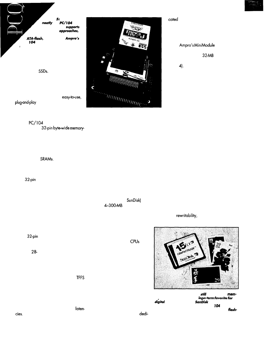
Photo
PCMCIA fits
into
applications and
all the key SSD
including linear flash (shown),
and NVRAM.
PC/
adapter (also shown) has
slots for two
PCMCIA cards.
and software-to effectively use NAND
flash chips as
By now, I’ve probably scared you so
badly you’re ready to turn the clock back
20years and return to ROM-based micro-
controllers. But, don’t despair!
There are quite a few
SSD
solutions ready to serve
your PC/l 04 embedded-PC needs.
BYTE-WIDE DEVICES
Most
embedded PCs include
one or more
device sockets. These were originally in-
tended for simple DIP or PLCC EPROM and
SRAM chips.
Using these devices, the capacity of a
32-pin socket is limited to 1 MB for EPROMs
and 5 12 KB for
Depending on the
SSD driver, multiple byte-wide sockets can
combine into a single DOS drive letter for
larger SSD capacity.
As
NOR flash surfaced, it’s been
supported like an EPROM, except that it
can be reprogrammed-usually on a full
device basis-inside the system.
The simple byte-wide SSD is pretty lim-
ited in capacity (comparable to a floppy).
Although a few PC/l 04 applications run
out of one or two simple byte-wide chips,
storage requirements have exploded with
CPU performance and
memory
availability.
A nice solution to the limitations of the
simple
byte-wide SSD is provided
by M-Systems’ DiskOnChip flash module,
shown in Photo 1. Although it’s the same
size as a
or 32-pin DIP EPROM, this
compact device has up to 2 MB of NOR, or
up to 12 MB of NAND, flash. Itcontains the
necessary circuitry to look just like a simple
DIP EPROM to the PC/l 04 CPU.
DiskOnChip comes complete with
and other support software for formatting,
operation, and maintenance. Future ca-
pacities are expected to reach 72 MB.
The
original
NOR
version
of DiskOnChip
(DOC 1000) had relatively slow write-cycle
time and long garbage-collection
However, the new higher capacity
58
version (DOC2000) benefits from the fast
write cycles and small erase block sizes of
NAND technology.
In fact, every memory technology I men-
tioned (i.e., NVRAM, EPROM, various kinds
of flash) is available on PCMCIA cards,
which are beginning to be called “PC
Cards,” by the way.
DRIVE-LIKE MODULES
Several companies now offer small size
(1.3” and 1.8” form factor) SanDisk flash
drives that look precisely like small IDE
hard disk drives (see Photo 2). They have
the same physical footprint, mounting holes,
interface connectors, and functional inter-
face as their magnetic media counterparts.
As a plus, PCMCIA cards are remov-
able. They can be inserted and removed
while the system is running, just like floppy
disks. They’re useful for storing data, load-
ing parameters, and updating firmware.
Since PCMCIA cards are popular for
laptop PCs, they are sold by all major
computer retailers at competitive prices.
With IDE flash, a microcontroller handles
all flash-management functions (e.g., wear
leveling), so no special drivers are needed.
IDE flash was pioneered and popularized
by
SanDisk
(formerly
and is avail-
able in
capacities, with higher
capacities on the way.
But PCMCIA cards require a special
PCMCIA card slot. You can’t just plug them
into a byte-wide memory socket or cable
them to an IDE interface. Instead, you need
a PCMCIA controller or interface module,
adding cost and complexity.
To use these tiny IDE flash drives, just
install and operate them like nor-
mal IDE drives. Nothing’s simpler!
If you don’t need them as removable
media, check out a DiskOnChip or an IDE
flash drive. On the other hand, you may
need NVRAM for its speed and truly unlim-
ited
and PCMCIA is the best
One possible catch: you need
an IDE interface in your system.
However, most PC/l 04
now
include IDE interfaces free.
One major advantage: IDE flash
drives are OS independent. All
operating systems provide IDE hard
disk support, and flash-manage
ment is handled by the drive. You
can replace the drive without wor-
rying about having the proper
driver for the specific flash technol-
ogy.
Photo 6: Although the jury’s
out on which
orv-card format will be the
PC/l 04 module? This option, too, is
readily available in a variety of formats.
PC/l 04 SSD modules come with four
or more 32-pin byte-wide sockets for indi-
vidual plug-in EPROM, SRAM, or flash
(e.g.,
in Photo 3).
They’re also available with soldered on
NOR flash for up to
SSD capacity
(e.g., the M-Systems PC/l 04 Flash Disk in
Photo
PCMCIA MEMORY CARDS
Last, but certainly not least, is PCMCIA
(see Photo 5). This well-known standard
offers a broad range of SSD capabilities.
PC/l 04 SSD MODULES
cameras, these tiny
Compactflash
Why not put EPROM, NVRAM,
cards certainly meet the needs of PC/
applica-
or flash SSD devices on a
tions requiring highly compact and removable
memory modules.
CIRCUIT CELLAR
INK JUNE 1997
way to contain high capacity, reasonably
priced NVRAM.
Incidentally, PCMCIA offers two differ-
ent flash-card configurations.
is functionally
identical to an IDE flash drive, except it’s
accessed through a PCMCIA card slot
instead of an IDE interface.
From a command-set perspective, it pro-
vides the identical system-level interface as
IDE. It’s even possible to create a passive
adapter between
flash cards
and standard IDE interfaces, eliminating
the need for a PCMCIA controller.
Like IDE flash drives, each
has an internal controller to handle
flash-management and IDE command-set
functions.
means
inter-
face. It’s just another name for IDE.)
The other PCMCIA flash approach cor-
responds to that used in the DiskOnChip
(see Photo 5). It is commonly referred to as
“linear flash” because the flash is indirectly
accessible (via bank switching) to the sys-
tem CPU as blocks of linear memory. The
required bank-selection logic is located
within the PCMCIA interface controller.
Although linear-flash PCMCIA cards
don’t bear
the
burden
internalcontroller,
this is also their biggest shortcoming.
With no internal controller to automati-
cally manage flash-memory wear-leveling
and erase/write functions, these tasks must
be handled by the system CPU, resulting in
reduced real-time performance and creat-
ing a degree of OS dependence.
Also, when you change cards, you must
ensure that your embedded system has the
right
driver
software to properly handle the
card’s internal flash technology.
NEWS FLASH
We can’t leave the subject of SSD for
PC/l 04 applications without looking at the
latestdevelopments-solid-statestoragefor
digital cameras.
Have you noticed ads for
digital
cameras? Photography’s going digital!
Whether this is good or bad for photog-
raphers, I can’t say. But for
em-
bedded systems, it means SSD
especially flash-is about to become less
expensive and more widely available.
Unfortunately, there isn’t a consensus on
exactly what tiny memory-card standard
will prevail. Sound familiar?
So far,
has
made the most inroads. Shown in Photo 6,
it’s essentially a shrunken version of
Like its big brother,
has
an IDE-like functional interface. It’s relatively
easy to convert from an IDE hard drive
interface to a
card socket.
While this sounds like a dream come
true for embedded systems needing minia-
ture removable SSD cards,
and two other tiny memorycard standards
are fiercely battling for dominance in the
digital-camera market.
For sure, you’ll be hearing a lot about
new
flash-memory
alternatives
to disk drives.
P U T T I N G I T T O G E T H E R
As you can see, PC/l 04 system design-
ers have many options. To help you evalu-
ate the alternatives, take a look at Table
I hopeyou’refeeling more
rather than more confused-than before. If
not, don’t worry. It’ll probably all come to
you-in a flash!
Rick
Com-
puters where he served as VP of engi-
neering from
1983
to 1991. Now, in
addition to his duties as
VP
of strategic
development, Rick chairs the PC/l 04
Consortium. He may be reached at
SOURCES
Computers, Inc.
990
Ave.
Sunnyvale, CA 94086
(408) 522-2 1 0 0
Fox:
(408) 720-l 305
DiskOnChip, TFFS
M-Systems, Inc.
4655 Old Ironsides Dr.
Santa Clara, CA 95054
( 4 0 8 ) 6 5 4 5 8 2 0
Fax: (408) 654-9107
Corp.
140 Caspion Ct.
Sunnyvale, CA 94089
(408) 542-0500
Fax: (408)
Intel Corp.
500 W. Chandler Blvd.
Chandler, AZ 85226-3699
( 6 0 2 ) 5 5 4 8 0 8 0
Fax: (602) 5547436
4 16 Very
Useful
4 17 Moderately Useful
418 Not Useful
E
IF YOU DO
FUNCTIONAL
YOU
NEED
EXTENDERS
Cards With PC Power On!
Save Time Testing And Developing Card!
Save Wear On Your PC From Rebooting
Adjustable Overcurrent Sensing Circuitry
NO Fuses, All Electronic For Reliability
Single Switch Operation W/Auto RESET
Optional Software Control Of All Feature
Breadboard Area For Custom Circuitry
And More...
Passive
PCI Extender
Passive
Extender
Passive MC32 Extender
Passive ISA Extender
AZ-COM, INC.
Fax on Demand:
510-947-l
000
Ext.7
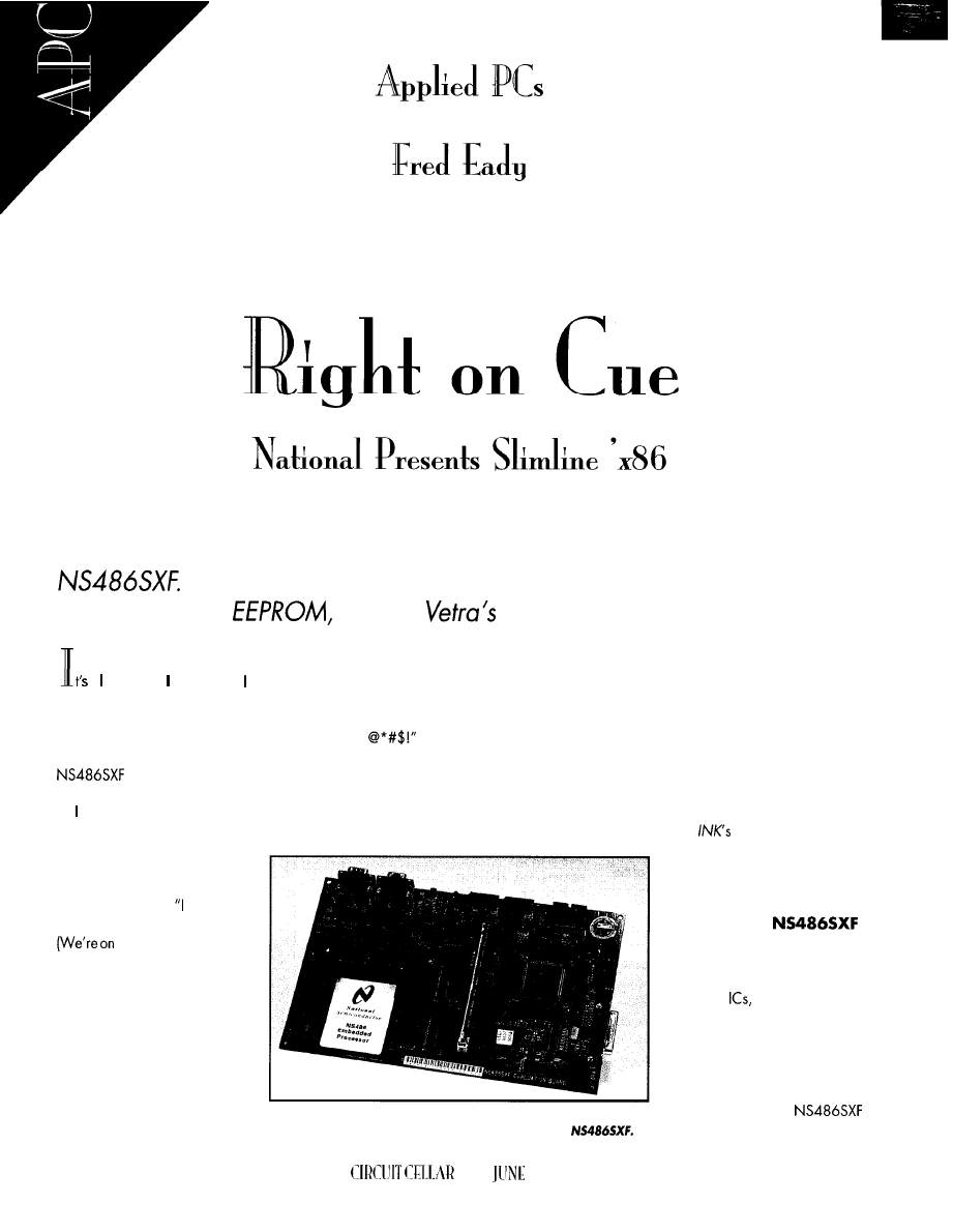
Fred measures and stores voltages at specified times using National’s
He shows how to get the
ADC
data into the ‘486 for processing,
store the data to
and use
Reverse Pipe for keyboard access.
t a most time. tense up as await my
cue. We’re on the air.
“Hi, I’m Fred Eady. Welcome to the
Circuit Cellar Florida Room. Today’s spe-
cial guests are National Semiconductor’s
and Vetra Systems’ Reverse
Pipe.” (Huge applause from the audience.)
I turn around quickly, drop the mic, and
trip over the cord. As I fall on my face in
front of a live studio audience, I mumble,
“Oh,
turn to greet my guests, and they’re
machines! A PC board filled with all sorts
of components and a rather tiny
black box laden with I/O connec-
tors sit by my desk!
Blahnn. Blahnn. Blahnn. Wake up, sleepy
head. I slap the alarm button and think
about how I hate that noise. Boy, another
weird dream. Better get up and get with it.
I’ve got an article to write.
Most guys sleep soundly and dream of
beautiful women, wealth, and fame. Not
me. My Vanna is a piece of embedded
silicon dressed in sexy software lace. My
wealth? It’s firmware that’s either gone up
in a flash or stored in a spinning magnetic
vault. Fame? Well, it’s the 15 minutes or so
a month from those of you thot follow my
adventures in
Florida Room.
But since this offering started
out as a talk show, let’s meet the
guests.
“Oh, no!” I think. don’t have
any software to make them talk!”
a talkshow, you know.)
I frantically
call
to the set’s best
boy, “Get my embedded develop-
ment software and that VIPer806
out here quick!”
I yell to the set director, Mark,
“Roll a couple commercials back
to back. That’ll give me time to get
these things hooked up! Did you
bring that Iittlex-ytable? We may
need it for fill.”
Photo I: This beauty can turn any embedded programmer’s head.
Note the abundance of header pins surrounding the
60
INK
1997
N A T I O N A L ’ S
Normally, when you think of
National Semiconductor, you think
components. You know-regula-
tors, logic
things like that.
Sure, there’s the National
COP8 series of microcontrollers,
but National never really spelled
“embedded” like you and I do.
For the next few minutes, we’re
going to put the new
evaluation board to work.
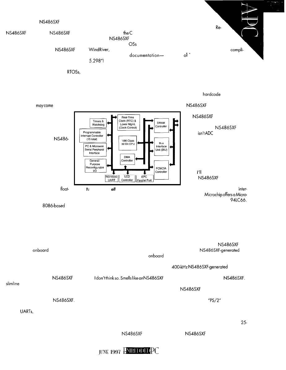
The heart of the
eval board
shown in Photo 1 is, of course, the
silicon. The
is an
embedded controller based on the Intel
‘486 32-bit processor.
Unlike its big brother, the
fits
into most embedded environments. With its
power-managementabilityand strong peri-
pheral set, it was born to be embedded.
This little guy can run most
including QNX. It uses standard +5-V power
and incorporates all the peripherals we
embedded types can’t do without.
Although the processor speed is limited
to 25 MHz, there are some special embed-
ded features that
in handy
for your applications. One of those
is the ability to reconfigure unused
peripheral pins for task-dependent
purposes. There’s also an IEEE-com-
pliant parallel port.
National describes the
SXF as a “system on a chip.” Hard-
ware functionality for most embed-
ded applications can be found in its
core. It’s petite, fitting nicely into
many embedded tight spots.
But, it gains this slimness by sac-
rificing some functionality. It differs
from the standard Intel part in that
All you need to get started is Bill’s or
Borland’s C. To help you along, the folks at
National include all
header file defini-
tions for the
register set
with
the
evaluation kit. Sample
from Microtec,
and Phar Lap are also there.
Oh, yeah. The
If you don’t have room on the
shelf, conserve space by viewing it on
National’s Web site.
THE MONOLOGUE
As a guy that uses the soldering iron as
much as the keyboard, I find myself poking
probes here and there to test voltages or
but there’s an extra serial
port. That’s where the
verse Pipe comes in.
As you see in Listing 1, a bit of
C code, the flip of a DIP switch, and
bap! It’s a keyboard interface,
Vetra’s VIP-345 Reverse Pipe converts
standard PC-keyboard keystrokes to ASCII
codes. It can also be programmed to pass
nontranslated voltage levels correspond-
ing to PC-keyboard scan codes.
A keyboard lets me write menu code so
I don’t have to
every test se-
quence. When you use the Pipe in your
ments the serial port.
real-mode, virtual-memory, and
Figure This baby’s that and a bag of chips!
ing-point support aren’t there. The
lack of real-mode support implies that any
conversion of older
embed-
ded apps will need some touching up.
If your potential application needs to
crunch numbers, be ready to take out your
code checkbook and write some big ones.
The only floating point you’ll find will be in
your software.
While the checkbook’s out, write one
for setting up
peripherals too.
They’re handy but code expensive. I spent
a great deal of time tweaking bits in vari-
ous registers to get the simplified code you
see in Listing 1.
The bottom line: the
is a
version of its Intel brother and is
ideally suited for particular types of embed-
ded applications. Figure 1 offers a simpli-
fied block diagram of the
The evaluation board includes flash,
DRAM,
PCMCIA, IR, and a real-
time clock laid out and ready to use.
There’s even a diskette with “it really works”
example code to exercise all the system
service elements or to include in your own
project.
look at waveforms on most of my little
creations.
Well, this particular collection of solder
globs requires logic levels to be applied to
certain points in the circuitry and subse-
quently change voltage levels at other
specified points. Since this group of parts
and pieces is a prototype, the whole pro-
cess is looking like manual labor to me.
To add to my misery, the voltage levels
must be recorded and loaded into
nonvolatile memory for tracking and iden-
tification. That implies multiple boards,
multiplevoltages, and multiple headaches.
application to me!
THE LINEUP
The key to most successful covert opera-
tions is to know your enemy and bring the
right weapons. Today’s weapons are com-
binations of various black boxes.
In this application, the Vetra Reverse
Pipe isoneofthose highlyeffectiveweapon
components. The
evaluation
board has no native keyboard interface,
application, be sure to
use a null modem between it and
the
board.
This app is all about measuring
voltages. The
eval
board
equipped, so that’s
got to be done externally. I don’t
need high resolution or speed, but
it’s gotta be cheap, so the National
ADC0809 suffices.
Once the voltages are deter-
mined, I have to store them. That’s
easy. use serial EEPROM.
The
has a set of pins
that can be configured for a
Microwire/Access.bus master
face.
And,
wire-compatible EEPROM in the
The plan is coming together. So far, I
can measure and store my voltages as well
as keyboard-alter my test sequences, thanks
to the Pipe. I also need to provide TTL-level
I/O lines to retrieve voltages and control
the prototype’s logic.
The ADC0809 is an 8-bit device that
won’t operate without an
8-bit
I/O port, three
ad-
dress lines, a start-conversion line, an ad-
dress latch-enable line, and a nominal
clock sig-
nal. To effect the ADC0809 subsystem, I
get these resources from the
Reconfigurable I/O to the rescue! I as-
sign
I/O pins for the address
and control lines as needed. As for the input
port, I use the ECP in
mode-a fancy
way of saying “standard parallel port with
bidirectional data capability.” I can recon-
figure the ECP port as bidirectional I/O
pins, but why waste a perfectly good
pin connector already on the eval board?
The
is loaded with three
8254compatible timer-counters. It really
61
Embedded
Midwest Micro-Tek is proud to offer
its newest line of controllers
based
the
architecture.
The
8031
comes at a surprisingly
low cost of $89.00 (100 quantity).
MIDWEST MICRO-TEK
2308 East Sixth Street
family
80386 protected mode
real mode
family
l
Compact,
fast
response
l
Preemptive, priority based task scheduler
l
Mailbox, semaphore, resource, event, list,
buffer and
managers
l
Configuration Builder utility
l
Comprehensive documentation
l
No royalties, source
included
For
of
Phone: (604) 734-2796
Fax:
734.8114
E-mail:
W e b :
KADAK Products Ltd.
V J
If you’re interested in getting the
most out of your project, put the
most into it. Call or Fax us for corn-
data sheets and CPU
MIDWEST MICRO-TEK
shows its embedded roots here. The
counter pins, including thegates, are
callyaccessible! Boom!
ADC0809 clocksource. The hardware parti-
culars can be gleaned from Figure 2.
B E H I N D T H E S C E N E S
With the problem defined and hardware
resources in place, let’s bring the project
alive module by module. I’ll start with the
ECP peripheral baseaddressed at 0x0278.
All ECP functionality is selfcontained in
the
ECP port operation is con-
trolled via the contents of the
parallel-port I/O control registers, which
are mapped in I/O space for easy access.
Of the six possible ECP modes of opera-
tion,
chose
mode. I en-
abled it by setting bit 5 in the Extended
Control Register (ECR) at location
The
three highorder bits deter-
mine which mode the port operates in. For
mode, the mask is 001. The remaining
ECR bits twiddle with the IRQ, FIFO, and
Since I’m not using the other
ECP modes, these bits are don’t cares.
Once the port mode is set, the only thing
left is set the port data direction. Since the
ECP is used for input only, I set bit 5 of the
Device Control Register (DCR) located at
address
to enable the ECP data
I/O pins as inputs.
If I needed bidirectional capability, I
could toggle the state of bit 5 in the DCR
using
(A Simple Matter Of Program-
ming).
I could determine whether
the ECP data pins were inputs or outputs.
The ECP is ready to roll. If the 0x0278
address looks familiar, it’s because the
architecture tries to-retain stan-
dard PC I/O addressing
where possible.
I N T E R V I E W I N G A - T O - D
Now I need three address lines and on
ALE (Address Latch Enable) line for the
ADC0809. These lines are part of an
multiplexer arrangement selecting
one of eight analog inputs. The ADC0809
also requires a start conversion (SC) pulse
I can piggyback onto the ALE line.
The analog-input
port address
is clocked
into the ADC0809 on the rising edge of the
says, write the wde
makes the whole
thing sing.
i n t m a i n 0
i n t i ;
turn on
mode
i 0x20:
set ECP direction bit
i 0x20;
disable LCD/PCMCIA functions
i
and steal pins 48-54 and 68-79
set stolen pins
output
write bit masks to RIO_DO_BYTEX
enable PIT and Microwire
i 0x88:
initialize PIT
initialize Microwire
i
set clock to 25 MHz
Initialize UART and baud rate here...
d
o
read char from Pipe and print to PC
return 0;
CIRCUIT CELLAR INK
JUNE 1997
SC pulse,
time. The
edge of
Since
or PCMC
their pins
dress
(RIO]
NS48
include
UART lint
LCD interf
interface
7oftheR
the LCD a
15 pins
As Fig
SXF pins
with pin
their
tion
The DI
locations
lays out
DDR bits,
although
an outpui
control
puts the
single-chi
scheme,
The
each
signals a
are outpu
makes sh
plexer
Next
(PIT) to
Progrc
by
identical
run-of-the
PIT is
Interface
2. This ta
of the
SC pulse, and the ADC is initialized at that
time. The conversion begins on the falling
edge of the SC pulse.
Since I’m not using the
LCD
or PCMCIA peripherals, can reconfigure
their pins as the ADC0809 multiplexer ad-
dress and latch lines. The Reconfigurable
I/O (RIO) Control Register lives at
reconfigurable peripherals
include four CS (chip select) lines, two
UART lines, the ECP port (eight lines), the
LCD interface (seven lines), and the PCMCIA
interface (eight lines). By setting bits 6 and
7 of the RIO Control Register, can disable
the LCD and PCMCIA functionality, freeing
pins for general-purpose I/O.
As Figure 2 shows, I assigned
SXF pins
and 70 as address lines,
with pin 71 acting as the ALE and SC pulse
generator. All these pins are outputs, and
their function is defined in the Data Direc-
tion Register (DDR).
The DDR is 32 bits wide and resides at
locations
The datasheet
lays out what pins correspond with what
DDR bits, so trust me. I chose the right ones,
although I thought it odd that 1 made a pin
an output and 0 signified an input.
Writing to o standard parallel-port
control register’s
lower nibble
puts the port’s pins in input mode. Most
single-chip controllers use the “1 is input”
scheme, too. To me, 1 denotes high-im-
pedance inputs and 0 is round for outputs.
The Data Port Out Register at locations
holds the output
values
of
each reconfigured pin. When the I/O write
signals are valid, this register’s contents
are
output
to the corresponding pins. Using
mnemonic
makes short work of the
multi-
plexer support.
Next task is to generate a nominal
clock for the
used the
Programmable Interval Timer
(PIT) to generate this pulse train.
Programming the PIT is accomplished
by manipulating I/O ports at locations
Implementing the PIT is
identical to the
devices found on
run-of-the-mill desktops.
Getting a square wave at the correct
frequency is no problem. First, I ensure the
PIT is accessible by enabling it via the Bus
Interface Unit (BIU) Control Registers and
2. This task is done by writing a 1 to bit 3
of the BIU Control Register 1 at address
Next, since the counters come up with
random
I have to program thecounter
I want to use. use Counter 1 at I / O
address 0x004 1.
The bit mask shown in Listing 1 selects
Counter 1 (bits 7 and
loads an
count word
(bits 5 and
sets squarewave
mode (bits 3, 2, and
and sets up
Counter 1 as a
binary counter (bit 0).
This byte is written to the Control Word
Register at address 0x0043. After entering
the control byte, a
count value is
loaded at address
is
value for Counter 1.
Finally, I make sure
the Timer Clock Register at
0x0045 is set to divide the
selected internal clock source by
16 and the Timer I/O Control Register
lets the clock pulses escape via
1 out pin.
I get a square
wave at pin 56 on the
that’s
real close to 400
(-389
The only A/D loose end left is the
ADC0809 EOC output. No problem.
ignore it. Conversion takes place in
-100
so I give it ample time in the final
code to do its thing. I’m in no hurry.
your source for the most
powered, comprehensive set of time-saving
software and hardware development tools for
embedded
development.
1: Paradigm
LOCATE the most popular tool for
creating embedded C/C++ applications with
Borland and Microsoft compilers; 2:
Paradigm
DEBUG the only x86 debugger
RTOS,
scripting language, and full
emulator
support; 3:
Paradigm
SUPPORT the best technical
support in the industry supplied to our
customers for free.
Developing real-time embedded applications doesn't have to be
time consuming or difficult-youjustneed to have the
Paradigm alone
has the high performance development tools you
need to
the embedded system software development
process so your Intel and AMD x86 applications are
record
time. Paradigm's complete suite of tools work with industry standard
C/C++ compilers from Borland and Microsoft, as
as hardware
Applied Microsystems, Beacon Development
Tools and other
Call us at 800-537-5043 today and Let take care of all your
development
needs, you can keep your focus where
you need it--on your application.
JUNE 1997
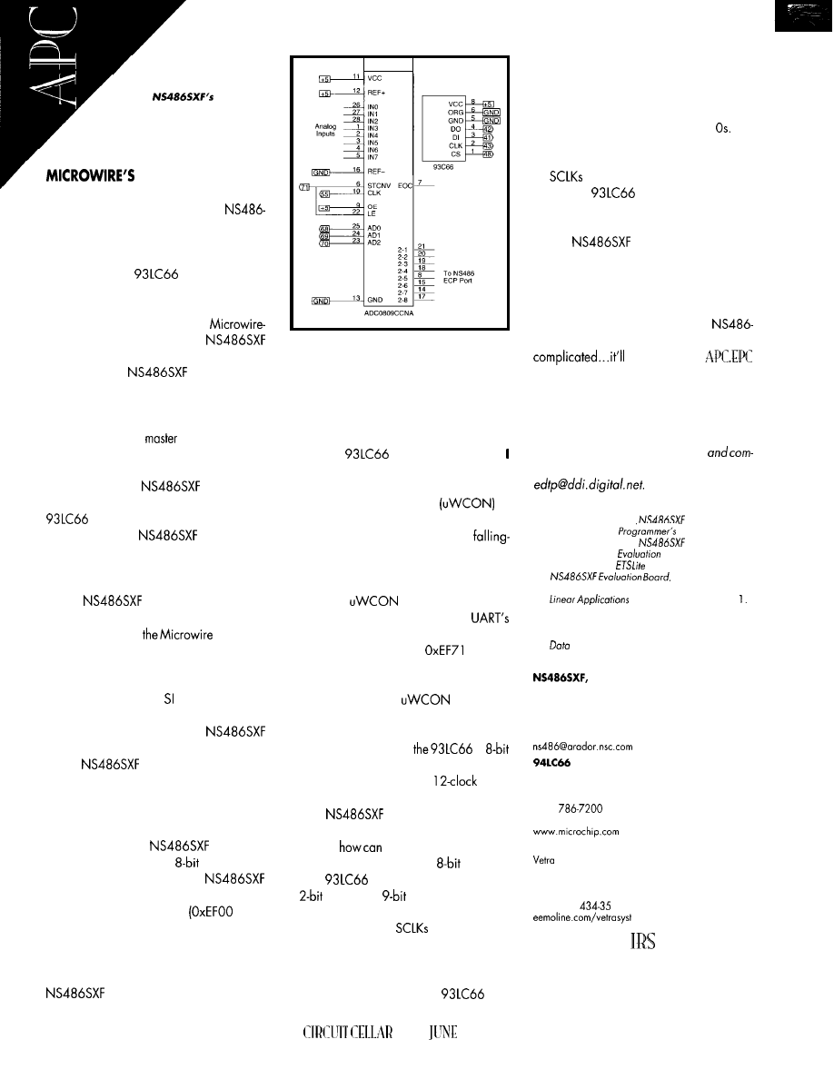
Figure 2: Not a single
glue part. All the decod-
ing and clocking are done
by the
firmware
and system service elements.
PERSONAL SIDE
Now that we can acquire voltage data,
we must be able to put it away. The
SXF Microwire interface can support the
standard three-wire serial interface. tots of
goodies can play with Microwire, includ-
ing Microchip’s
serial EEPROM.
Microwire is a three-wire synchronous
serial bus. The serial input pin (SI) receives
synchronous data transfers from
compatible peripherals. SI is
pin 42.
Conversely,
pin41 (i.e., the
SO, serial output pin) drives data to Micro-
wire clients. Since it’s a bus-oriented proto-
col, several devices can be present on
Microwire’s bus. So,
and
slave modes
can be implemented, depending on how
you use a particular Microwire device.
For now, the
will be the
Microwire bus master, with the Microchip
acting as the slave. This arrange-
ment means the
supplies the
Microwire clock (SCLK) at its pin 43. I’m not
concerned with addressing details-I’m only
driving a single slave from a single master.
The
SIO (serial I/O) register
is an 8-bit shift register that transmits and
receivesdata from
interface.
Data is shifted out through the SO pin, most
significant bit first.
Similarly, incoming data is shifted into
the SIO register via the pin, implying that
both transmit and receive functions are left
shifts within the register. The
SIO register is I/O mapped at 0x005
1
h.
The
Microwire interface per-
forms send and receive operations at the
same time. Input data is sampled on the
rising edge of SCLK, and data is driven to
the output pin on the falling edge. In the
case of the internal
Microwire
interface, it’s always an
transfer.
Here’s how
I
activate the
Microwire interface. I set the master Micro-
wire enable bit in the BIU
bit 7)
and enable its interface via the Microwire/
Access.bus Control Register (MACON).
Setting MACON bit 2 at 0x0050 does this.
As the register’s name implies, the
Microwire interface can also
64
be used as an Access.bus interface. Bit 1 in
the MACON lets me choose my mode of
transportation.
I
clear bit 1 to select Micro-
wire’s interface. The MACON’s remaining
bits fiddle with the interface clock frequency.
Since I’m in no hurry, I set the clock well
below the
datasheet guidelines.
can always tune it later.
The next step tickles bits within the
Microwire Control Register
at
address 0x0052. Bit 2 must be clear to
allow the Microwire rising- and
edge data transfers.
Setting this bit produces the opposite
effect. Microwire master mode is selected
by setting
bit 1. The interface
shares its pins with some of the
modemcontrol signals. Bit 2 in the Modem
Signal Control Register at
must be
cleared to activate the Microwire signals.
When I’m ready to plug data into the
EEPROM, bit 3 of the
sets off the
process. This BUSY bit starts a transfer cycle
and serves as the shift-register busy flag.
Reading and writing
in
mode uses 20 SCLK cycles. Also, it must be
erase/write enabled via a
com-
mand sequence before accessing storage.
The
Microwire interfacecan
only do one 8-bit transfer per Microwire
cycle. So,
I command the EEPROM
and get data, too, using an
cycle?
The
data packet has a start bit,
a
opcode, a
address/command
field, and 8 bits of data. Add up the bits.
That’s where the 20
come from.
The erase/write enable (EWEN) and
erase/write disable (EWDS) commands
are formatted the same way with no data
at the end of the packet. The
start
INK
1997
bit is detected when CS (Chip Select) and
DI (Data In) are both high with respect to a
rising SCLK edge.
So, I pad the high-order nibble of the
first Microwire transfer cycle with
The
start bit is detected in bit time 5 of the first
8-bit transfer, and the rest of the packet’s
16
transfer the instruction and data
just as the
likes to see it.
THANKS FOR TUNING IN
The
offers modularity that
can’t be found in its Intel ‘486 big brother.
But, it takes a lot of code to replace the
number crunching of a math coprocessor.
But, if your application can live without
some of the comforts of home, the
SXF project you end up with won’t be
beembedded.
Fred Eady has over I9 years’ experience
as a systems engineer. He has worked with
computers and communication systems
large and small, simple and complex. His
forte is embedded-systems design
munications. Fred may be reached at
REFERENCES
National Semiconductor.
Embedded
Microprocessor
Guide, 1996.
National Semiconductor,
Embedded
Microprocessor
Board Manual, 1996.
Phar Lop Software,
User’s Guide for the
1996.
National Semiconductor, Notional Semiconductor
Handbook, AN-247, 199
Microchip Technology, Serial EEPROM Handbook,
1994.
Microchip Technology, Non-Volatile Memory Products
Book, 1995-l 996.
SOURCES
Microwire
National Semiconductor Corp.
2900 Semiconductor Dr.
Santa Clara, CA 95052.8090
(408) 72 l-5000
Fox: (408) 739.9803
Microchip Technology, Inc
2355 W. Chandler Blvd.
Chandler, AZ 85224.6 199
(602)
Fax: (602) 786.7277
Reverse Pipe
Systems Corp.
275-J Marcus Blvd.
Hauppauge, NY 1 1787
(5 16) 434-3 185
Fax: (5 16)
16
419 Very Useful
420 Moderately Useful
42 1 Not Useful
DEPARTMENTS
Hugh
Machine Vision
Industrial Inspection
y friend was part
of an engineering
team installing a newly
developed inspection sys-
tem in a manufacturing plant.
A status lamp indicating normal
operation refused to turn on. Despite
having an in-circuit emulator, software
debugging tools, and an oscilloscope,
they couldn’t find the problem.
After several frustrating hours, a
plant electrician stopped in to drawl,
de bubs gawn.” An embarrassed
engineer held up the evidence-a failed
light-bulb filament.
Funny as it sounds, this story is
typical. Given so many complex inter-
actions in the system, we naturally
suspect failures in the timing, special
hardware, or software. Too often, we
overlook the obvious.
There’s an important distinction
between using machine vision as a
technology and developing an inspec-
tion machine.
An inspection system is a complete,
integrated quality-control tool that uses
various sensing methods (e.g., machine
vision) to solve manufacturing prob-
lems. To be useful, machine vision
requires integration into an overall
system.
there are ways to solve a problem
without using vision, tend to evalu-
ate them first. Sometimes, a different
66
Issue 83
June 1997
Circuit Cellar INK@
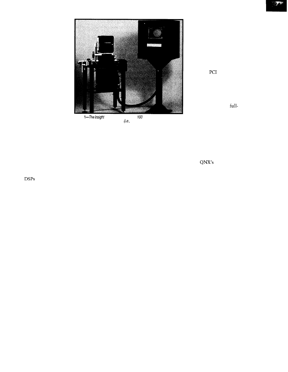
sensing technology provides a
simple and elegant solution.
But, certain inspection prob-
lems are best solved with a
camera-based system. And,
vision is increasingly making
its way into manufacturing.
Photo 1 shows the Insight
100, a turn-key commercialized
inspection system. It inspects
closures (i.e., bottle caps) for
the pharmaceutical and bever-
age industries.
In Photo 2, the system is
rejecting a defective child-resis-
tant cap with a liner that wasn’t
correctly punched.
Taking basic video-capture
technology and making it an
system used for high-speed closure
cap) inspection.
integrated inspection system is a costly
and involved development process.
Success requires talent in a number of
areas-mechanical, optical, electronic
hardware, software, mathematics, and
algorithm development (and don’t
forget the light bulb).
needed to help solve process problems.
And, new defects may become an issue.
USING INSPECTION SYSTEMS
Inspection systems can be used in
complementary ways.
And, it doesn’t impress the end user
if the system has the latest VLSI hard-
ware or
when the user interface
requires the skills of a rocket scientist.
But, a user-friendly system also won’t
succeed if it doesn’t solve the problems.
When sorting, they try to eliminate
defective products from the manufac-
turing process. This task is especially
important in high-speed applications
where human visual inspection isn’t
well suited. Even in slower processes,
people get tired, bored, or distracted
and can be very subjective.
SOLVE A REAL PROBLEM
Only by fully understanding the
problem and applying complex tech-
nology simply and intuitively can you
create inspection systems that are
useful to the factory floor operator.
When inspection problems aren’t
well defined, there’s a tendency to build
extremely flexible systems that solve
almost any problem. Conversely, if a
system is too easy to use and narrowly
focused, it limits market potential.
Automatic inspection systems also
provide vital data for understanding
and improving the manufacturing
process. Even in a simple configuration,
an alarm from the inspection system
can halt the process and notify the
operator that a defect limit is exceeded.
A balance between flexibility and
ease of use must be achieved. Even
with careful problem definition, I now
expect some changes while designing
an inspection system.
In a more advanced configuration,
the inspection system interfaces elec-
tronically with the manufacturing
machinery to automatically control
the process directly. So, an inspection
system that verifies label placement
on a box can tell the manufacturing
equipment to adjust the position.
New or hidden requirements often
materialize. Improvements in the
manufacturing process may demand
higher speeds. Or, color or material
variations needed by the customer may
cause changes to optics and algorithms.
Also, new product designs may
appear. More inspection data may be
You can also interface all inspection
systems to a data-collection server
over a network, making remote data
collection, analysis, and reporting
functions available plant-wide. A
phone-line interface to the server’s
modem offers remote diagnostics,
software upgrades, and problem resolu-
tion between the inspection-system
vendor and the plant.
A SIMPLE MODEL
Photo
Control Systems model
is a turn-key inspection
Figure 1 depicts an inexpen-
sive vision system that uses a
PC with a
frame grabber,
camera, and strobe. A separate
SBC tracks inspected parts.
An elementary system
using these components offers
real-time inspection at moder-
ate speeds. It’s not a
blown inspection system
since I won’t address many
important details [e.g., me-
chanical handling, packaging, and
internationalization of software).
I focus on system architecture and
integration of software and electronic
hardware. I chose MS-DOS and Borland
C to program this simple model, but I
normally use
32-bit RTOS. I
strongly advise using a real-time, multi-
tasking OS for serious development.
This system sets up the camera,
tracking, registration, inspection zones,
and a few rudimentary image-inspec-
tion steps to detect defects on a washer.
In this series, I discuss the
requirements, design trade-
offs, and problems typically
encountered in developing a
machine-vision inspection
system.
INSPECTION STEPS
Oversimplifying somewhat, inspec-
tion consists of performing these steps
in sequence:
l
sense the presence of the part to be
inspected (i.e., “part in place”)
l
track the part until it’s in front of the
camera, and then issue a trigger
signal to the frame grabber, which
coordinates a strobe flash with
image acquisition. Using a strobe
and shielding the camera from am-
bient light eliminates motion blur.
l
analyze the image to locate the in-
spected part and determine regions
of interest (ROI) for inspection
l
execute inspection algorithms in
each region
l
track a defective part to the reject
point and remove it from the con-
veyor via a mechanical flipper or
blast of air
l
update inspection counters, display
an image of the defective part with
Circuit Cellar INK@
issue 83 June 1997
67
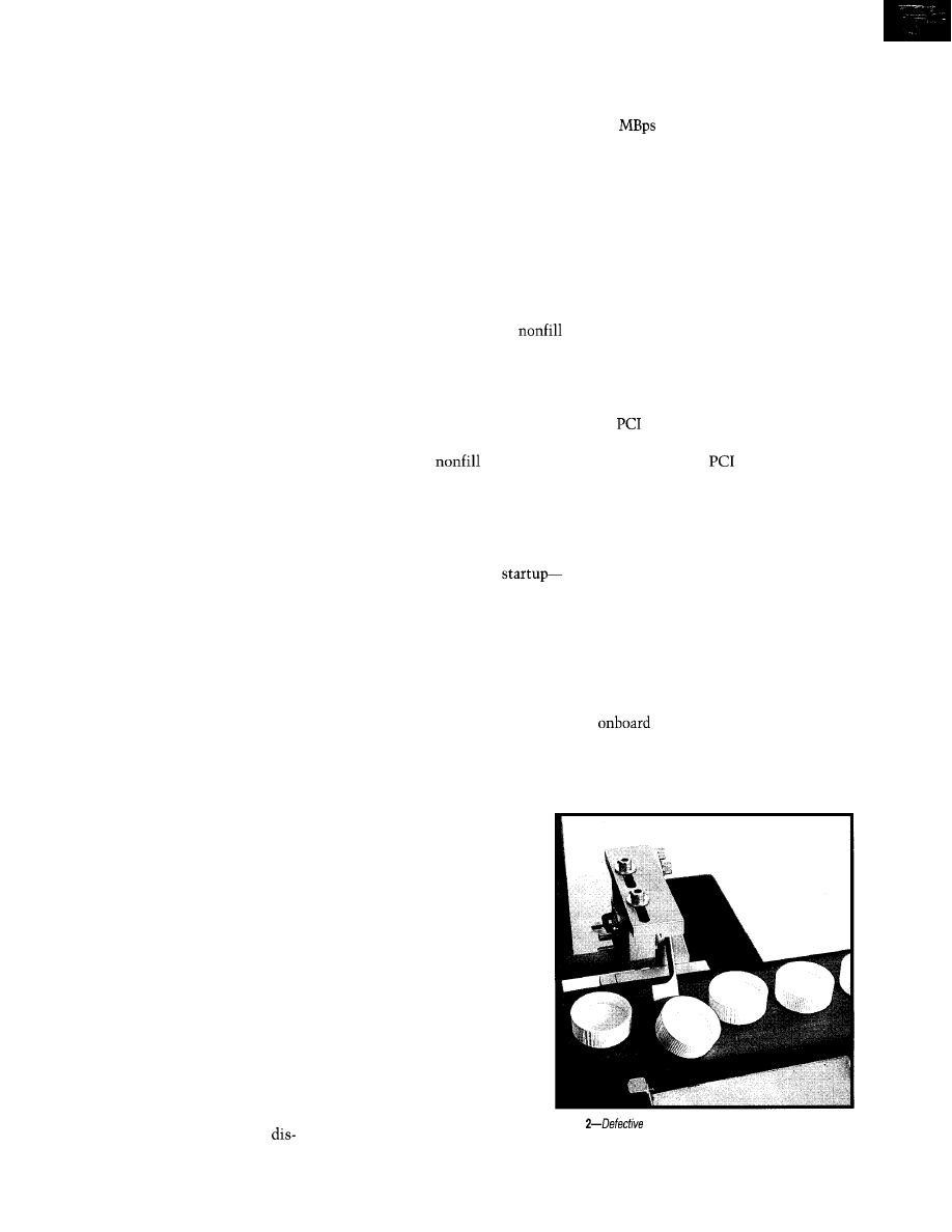
the defects noted, and update pro-
cess-control interfaces
Most steps must operate asynchro-
nously with respect to the others. For
full performance, acquisition, process-
ing, and display must be able to over-
lap in time.
As for software, this description is
just the tip of the iceberg. About 70%
of the software goes into developing an
interface that enables the user to easily
configure and maintain the system.
SOFTWARE REQUIREMENTS
A number of software modules
should be included in an inspection
system. Let’s discuss each of them.
Camera setup offers a user interface
to camera and frame-grabber controls
(e.g., gain, reference values, digital
filtering, etc.). You should be able to
acquire images as they pass in front of
the camera or continually acquire im-
ages of a static part by flashing a strobe
at a constant rate (autostrobe mode).
A tracking-setup module lets the
user set the correct timing for image
acquisition and rejection. This menu
must be fully interactive so the user
can tell when the image acquisition
and reject timing is right.
By differentiating its features from
background clutter, registration setup
trains the system how to locate the
part and find inspection regions relative
to the registration point(s).
Inspection setup lets the user estab-
lish sensitivity levels for each inspec-
tion algorithm. It must be interactive,
showing pass/fail status on a test image.
Job management provides storage
for sets of set-up parameters related to
a certain product type. Image file man-
agement loads and stores filed images.
Run-time inspection setup lets the
user fine-tune inspection sensitivities
while the machine inspects parts on-
line. The run-time screen displays a set
of counters and computations showing
inspection speed, number of inspections
and rejects, failure rate, and a break-
down of failures by each inspection
test.
This screen should support several
views of inspected parts. Viewing each
part as it goes by is of limited use. The
images update too fast. However,
68
Issue
83 June
1997
Circuit Cellar
INK@
play mode should be supported as it
can indicate whether the system fails
to reject defective parts.
A more useful display mode-freeze
on reject-updates the display when
parts are rejected. The ability to only
view rejects provides important process
information and is a valuable tool for
detecting false rejects (something that
should have passed inspection).
and 5 12 x 480 pixels, with 8 bits per
pixel to allow 256 shades of gray. At
600 ppm using 5
12 x 480
resolution,
2.5
of bandwidth is used per full
image operation.
Photo 3 shows the run-time screen
for the Insight 100 running in 256 x 240
resolution. In display all rejects mode,
the system displays a beverage cap with
a break in the seal area (i.e., a
or void] caused by uneven distribution
of the liner material.
In the past, standard computer buses
weren’t able to handle this load. Most
machine-vision manufacturers designed
special hardware with dedicated image
buses, but they were typically large,
proprietary, and expensive.
A more advanced method of freeze
on reject lets the user freeze on one
specific inspection step. For instance,
the option can be selected to only view
rejects when the
tool fails.
In recent years, more vision systems
have been available commercially, and
costs decreased as systems migrated to
PCs. Newer buses (e.g., PCI) are fast,
but they still fall short for heavy-duty
vision applications unless the load is
divided carefully among several pro-
cessing components.
Finally, the software may require
internationalization. If you’re design-
ing a commercial inspection system, it
must support the local language. I make
systems bilingual, so two languages are
loaded into the software at
one for the plant and the other for field
service technicians.
transfer rates vary between PC
manufacturers, so be careful if you
depend solely on
bandwidth for
system performance. Total bandwidth
is not a sufficient metric. Instead, the
evaluation must consider simulta-
neous availability of bandwidth for
acquisition, processing, and display.
VISION-SYSTEM ARCHITECTURES
Several types of systems are avail-
able in the PC-based vision market.
STARVING FOR BANDWIDTH
One of the biggest problems in
machine vision is having enough band-
width for acquiring, processing, and
displaying images in real time. Ideally,
the system handles all three tasks
simultaneously while tracking parts,
managing user interaction, and updat-
ing process-control interfaces.
A PC and frame-grabber system is
mainly suitable where inspection rates
are low or the processing requirement
is light. Some frame grabbers have
caching and enough intelli-
gence to capture an image from a hard-
ware trigger asynchronously without
host CPU interaction.
Although line speeds vary
across industries, it’s common
for systems I design to operate in
the ranges of 400-2500 parts per
minute (ppm). When inspecting
at 600 ppm, there are -100 ms
between parts.
This speed is approximate
since parts may not be evenly
spaced, causing inspection speeds
to burst occasionally. The system
needs enough extra performance
capacity to handle bursts with-
out missing inspections or going
south.
Frequently used image resolu-
tions for high-speed industrial
inspection are 256 x 240 pixels
Photo
closures must be eliminated from production.
The cap being rejected has a flaw in the cut of the liner material.
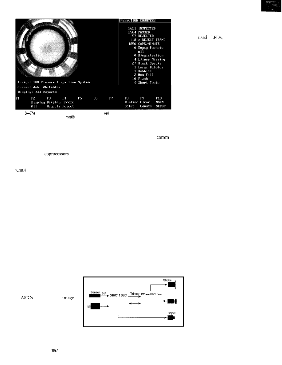
Photo
run-time screen should show process statistics, as
as enabling the operator to select the display
mode, c/ear production counters, and
the inspection sensitivity while the system continues to inspect.
If more than one camera is used,
caching and asynchronous operation
are critical. Except for very slow-speed
applications, the only suitable PC bus
is a high-speed one like PCI.
In PCs with
(e.g., DSP,
RISC, CISC) and frame grabbers, some
of the newer processors
(e.g.,
the TI
are extremely powerful pixel
bangers. But, you may have to write
highly optimized assembly code.
This multiprocessing architecture
clears up some bottlenecks, but it can
keep you reaching for the aspirin. Co-
ordinating processes across multiple
processors and designing in robust error
recovery is complicated. Processor
dissimilarities between the host and
coprocessor (e.g., byte ordering and
data alignment) need to be considered.
A PC with special hardware and a
frame grabber normally offers a limited
set of very fast image-processing func-
tions. Additional analysis or processing
may be necessary on the host PC. A
high-speed bus to the special hardware
and frame buffers is a big advantage.
The PC, running under an RTOS,
serves as the system controller, han-
dling the user interface and the
link between the tracking and process-
ing sections. A high-speed bus con-
nects the PC and vision processors.
LIGHTING AND OPTICS
Finding the right lighting technique
is the first step in evaluating the use of
machine vision in any application.
Most real-time image-analysis software
requires the inspected part to be illumi-
nated so that any defects cause a con-
trast, color, or other change.
In more difficult inspections, more
than one lighting technique is needed
for 100% defect detection. Defects
visible with one technique disappear
with another. Look for a more general-
ized lighting technique or use multiple
cameras and optical assemblies.
The topic of lighting and optics is
huge. Cognex’s minicourse proffers a
fundamental exposure to the subject
and useful course notes. In fact, they
offer an excellent one-week course in
machine-vision fundamentals for engi-
neers with a strong grasp of C.
Three types of light sources are
commonly
strobes, and
various constant light sources. I cover
their pros and cons in Part 3. My ex-
ample system uses a commercial Xe-
non strobe with a fiber-optic light ring
and diffuser.
CAMERAS
Camera technology is advancing
rapidly, resulting in a wide range of
new capabilities in a smarter, smaller,
and faster package. They’re also con-
fusing, due to a lack of standardization
both in function and terminology.
A few years ago, I found myself
refereeing between my camera and
frame-grabber suppliers. After the
discussion circled a few times, it be-
came apparent that we were suffering
the Tower of Babel syndrome.
They were arguing over a subtle
timing issue related to even and odd
fields of video. But, one supplier num-
bered the fields 0 and 1, while the other
used 1 and 2. Once terminology was
resolved, the technical issues were, too.
For very high-speed applications, use
a camera with a high-speed random-
reset capability. Be careful you under-
stand the timing and side effects when
using special camera modes.
Some cameras accumulate ambient
light while waiting for a reset pulse,
which can cause blooming in the im-
age. Other cameras advertising random-
reset capability require a considerable
time delay to reset.
Of course, I’m still looking
for the ideal vision engine that
balances hardware- and soft-
ware-based processing.
can be used for
Frame Grabber
Camera
processing functions requiring
RS-232
fast, repetitive neighborhood
processing (e.g., histograms,
Encoder
convolutions, morphology, etc.).
A high-speed processor per-
forms intelligent postprocessing
Figure l-Here, you see the major components and interconnections in a
to arrive at a pass/fail decision.
simple inspection system.
An inspection system’s display
often poses difficult technical issues,
since it must display both images and
the user interface.
You could use two moni-
tors-one for images and the
other for the user interface.
However, the system packaging
tends to become too bulky, and
real estate is often at a pre-
mium.
Using two small monitors
sounds good until you check
prices. If you need multiple
cameras later, do you add a
monitor for each?
DISPLAY
70
Issue
83
June
Circuit Cellar INK@
“We’re impressed by the
documentation
the readability
of the code. M.
“We
pleased
with the
BIOS and
forward to working with you to bring
product
to market. R.
Embedded BIOS is well-structured
and documented, and technical
at General
is
sure we made the right
decision to buy our BIOS
General
“‘Embedded BIOS is really
embedded PC designs.
You
absolutely right J
You Should Choose Embedded BIOS, Too
BIOS, DOS, Flash Disk With One low Royalty
Instant Boot, Console Redirection, Much More
Expert Support with Guaranteed Response Time
We Work Closely With
AMD, Intel,
to Deliver you a Proven, Tested, Feature-Packed BIDS
Millions of Units Already licensed
BIOS Adaptation Kit Includes:
Complete Source Code
Binary Configuration Program
Quick
+ Over 600 Pages Printed Documentation
General Software, Inc.
3 2 0
108th Ave. N.E., Suite 400
WA 98004
T e l : 2 0 6 . 4 5 4 . 5 7 5 5 . Fax: 206.454.5744 S a l e s : 8 0 0 . 8 5 0 . 5 7 5 5
E-Mail:
Cimetrics’
you can link together up to 250 of the most popular and
16-bit microcontrollers
68332,
The Q-Bit
is:
Fast-
A high speed
baud) multidrop
master/ slave RS-485 network
Compatible with your
microcontrollers
Robust
CRC and sequence
number error checking
.
Low microcontroller resource
requirements (uses your chip’s built-in serial
Friendly-
Simple-to-use C and assembly
language software libraries, with demonstration
programs
Complete- Includes network software,
network monitor, and RS-485 hardware
.
is an asynchronous
adaptation of IEEE
55
Temple
Place
l
Boston, MA 02111-1300
l
Ph 617.350.7550
l
Fx 617.350.7552
72
June
1997
Circuit Cellar
A dedicated image monitor may
also have a downside if the vision
hardware doesn’t provide a nonde-
structive graphics overlay. You then
end up drawing directly to the image
buffer, which is a
if you
need to reuse that image. Of course,
software may repair screen damage.
Single-monitor displays also pose
some design challenges, since the
image and user interface share a screen.
Some vision systems have direct
overlays over the image. Others use a
dedicated window for image display
and arrange the user interface around it.
In windowed systems, though, the
display must run in very high-resolu-
tion graphics mode, requiring a large
monitor.
Whatever technology you choose, it
should display images with graphics
notations to mark defects in real time
little performance penalty. Other-
wise, you’ll have to make significant
compromises in system performance
to work around the deficiency.
And, avoid display methods that
subsample the inspected image. Small
defects can be hidden, leading the
operator to incorrectly assume that the
system has a problem with false re-
jects.
Now that you have the background,
you’re ready for Part 2. I’ll cover a
complete tracking system using a
Motorola
SBC.
q
Hugh Anglin is a systems engineer
with experience in real-time and em-
bedded systems, process control, and
machine vision. You may reach him
by E-mail at
.com or by phone at (918) 3422248.
Lighting and Optics Workbook
Cognex Corp.
One Vision Dr.
Natick, MA 01760-2059
(508) 650-3105
Fax: (508) 650-3332
422
Very Useful
423 Moderately Useful
424 Not Useful
It Can’t Be
A Robot
Jeff Bachiochi
JUST A TOY
Part 1: There are
No Arms and Legs!
here do you think
you’re going?”
“Be-dop be-doop.”
“Well, I’m not going that
way. It’s too rocky. What makes you
think there are any settlements that
way anyhow!”
biddy biddy ba-werp.”
“Don’t get technical with me. I’ve
had just about enough of you. Go that
way. You’ll be sandlogged within a
day, you nearsighted scrap pile.”
It’s not the kind of conversation that
comes to mind when we think of com-
puters communicating. It’s more like
an act from the Comedy Club circuit
rather than from a protocol
and
astromech droid
lost in the
Jundland desert on Tatooine.
I cheer George Lucas and those who
pioneer the existence of robotics from
Gort through Data. Our technology
may not be on the same plane as our
dreams and fantasies, but those dreams
and fantasies drive technology forward.
One reason robotics is so popular is
because it touches on so many
motion, sensing, power, and intelli-
gence. Improvement in one area can
dramatically alter other fields.
Don’t tell my wife, Beverly, but I
like flipping through catalogs. Not the
Walter Drake or Harriet Carter stuff
she reads, but good stuff like Mondo-
tronics and Edmund Scientific.
I keep my eyes peeled for unusual
items. Tons of robot kits saturate these
catalogs. Thing is, most kits only per-
form a specific function: follow a line,
move toward light, hug the wall, avoid
falling off a table top. As teaching tools,
these kits have carved out quite a niche.
Toys, however, are for fun. Although
there’s some truth to the saying “the
bigger the boy, the bigger the toy,” I
believe the toy’s cost is not what makes
it delightful.
Tamiya, a Japanese company, has
an impressive line of motorized toy
vehicles.
I
was a bit apprehensive about
spending $40 when I had no idea of its
quality.
I
was even more frustrated to
learn the kit was discontinued.
Scurrying back through the catalogs,
I found an alternative from Mondo-
tronics. Photo 1 shows the parts of the
Power Shovel/Dozer kit.
What’s so impressive about it? The
three electric motors have
Photo
supplies
a co//age of park made from wood, metal, plastic, rubber-whatever the job.
74
Issue 83 June 1997
Circuit Cellar INK@
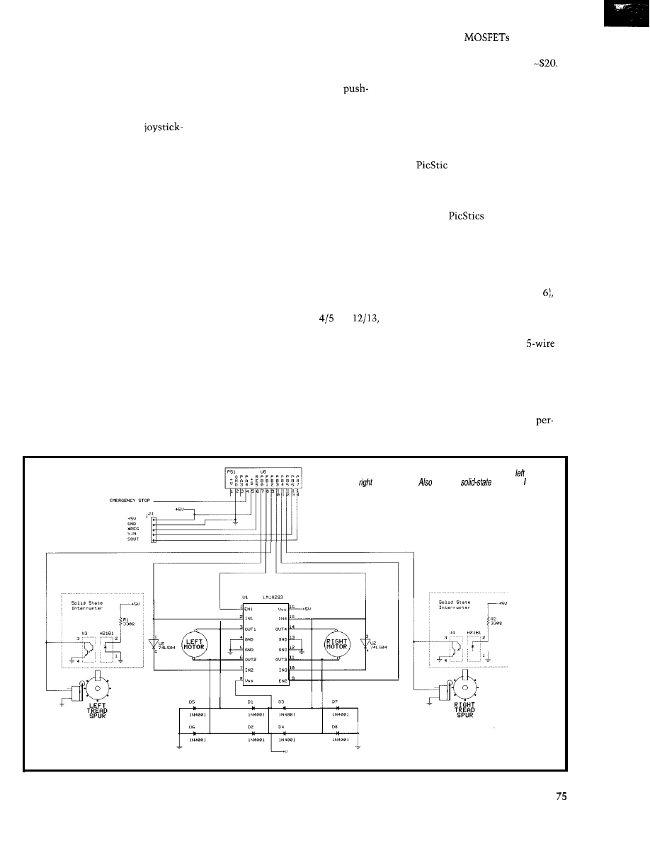
bled gear boxes giving a good mix of
torque and speed. The independently
controlled rubber tracks make moving
By rotating the tracks in opposite
directions, you get a tight turning ra-
over small obstacles a breeze.
dius. Using only two 1.5-V D cells, you
gain motor control through
type switches at the end of a 3’ umbili-
cal cord. The major holes are predrilled.
It would be easy to assemble-even for
an 8-year-old.
EDUCATIONAL PLATFORM
Some might suggest I’m copping out.
Surely, I should design it from scratch.
Essentially, I agree, but I want to
spend the time I have controlling the
beast, not fabricating one. So, I’m going
to use a known quantity and add mo-
tion, sensing, and maybe even a wee
bit of intelligence.
Constructing the Dozer took less
than 2 h. After taking it on a few spins,
I dug out the multimeter and measured
the current draw of each motor.
I measured -0.5-A continuous run-
ning current with peaks of -0.75 A.
Using the seat-of-the-pants 2x rule, I
searched for motor drivers that could
handle 1 A continuous. I wanted the
parts to be accessible.
National’s LM18293 jumped out of
the databook, and it’s available from
This single device has quad
pull drivers. It can be used to form two
Digi-Key. It was on National’s Web
H-bridges, one for either motorized
page, so I knew it wasn’t on death row.
tread. With an H-bridge, the motor can
run in both directions without needing
a bipolar supply. The only thing miss-
ing was internal protection diodes.
Figure 1 illustrates how I used the
‘18293. Each H-bridge is formed with a
pair of push-pull amplifiers, each hav-
ing two inputs and sharing an enable.
To be configured as an H-bridge, the
inputs must be driven by opposing
logic. If the inputs are both driven high
or low, there’s no potential across the
motor. An ‘04 inverter kept the inputs
opposed.
across the motor. Not terribly efficient,
but at $5, it’s at least cost effective.
This device uses transistor junctions.
The more expensive parts (e.g., an
The motor drive IC was shown to
have webbed legs on pins
and
but the parts I received didn’t have
them. These ground pins are beefed up
to also give heatsinking for the chip.
The drop across each driver is about
1.5 V, so I needed -5 V just to get 1.5
LMD18200) use
so the drops
are considerably less. But, they are a
single H-bridge device and cost
If
you substitute a pair of these, they’ll
cost as much as the motorized platform.
MOTION
To control the motor driver, I used
a micro. To keep costs low and the
programming environment friendly, I
used
1.
The reprogrammable
flash memory let me change BASIC (or
assembler) programs easily-my form
of experimental nirvana.
I’ve used
a lot lately. It’s a
friendly device for those who always
wanted to play around with micros but
didn’t dare to, given entry-level costs.
Whenever possible, I define the
upper two bits of the I/O port as serial
output (bit 7) and serial input (bit
even if the project doesn’t require
serial communication of any kind.
deep within the bowels of a project.
The open-collector mode of the
serial communications protocol
mits simple networking. The se r
i n
It’s a useful debugging feature, and
it enables me to use the same
networking connection on all my pro-
jects. The same connections can then
reprogram the micro even while buried
Figure l--This schematic outlines the controls for and
tread motors.
note the
encoders
rep/aced with microswitches.
Circuit Cellar INK@
Issue 83 June 1997
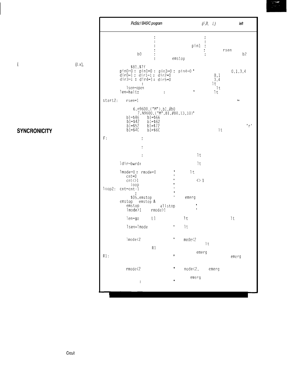
statement ignores all communication
until a particular character sequence is
recognized, so you can keep other
micros hanging on the same bus from
interfering with private conversations.
I use the capital letter M as a single
addressing character followed by one
of four 2-byte commands-forward
Fx), backward (Bx), left turn
and
right turn (Rx), where
x=1-255
counts
(0 being continuous). A count is a
specific unit of distance measurement.
The only difference between mov-
ing forward/backward and turning is
that the treads move in opposite direc-
tions instead of moving in the same
direction. The base rotates about its
center in a tight radius, making the
platform highly maneuverable.
The twin DC motors that indepen-
dently move the left and right treads
run at different speeds depending on
friction and load presented to each
motor. Therefore, starting and stopping
them together doesn’t assure that both
treads move the same distance.
Although the treads can indepen-
dently slip in relation to one another,
it’s helpful to keep the dual drives in
sync. To do this, you track the distance
traveled by each drive train, perhaps by
using shaft encoders. However, this
vehicle has components that lend
themselves to tracking distance.
The front wheels have three equally
spaced holes that can be used to count
wheel rotation (distance) by one-third
or about a linear inch between hole
rotations. The rear wheels have teeth
that engage the plastic track. The gear
teeth are spaced about every 0.25” and
provide better resolution.
Remember when floppy disk drives
were open framed and you could see
their inner workings? The head move-
ment was usually initialized to track
zero by moving the head back and forth
and sensing when a plastic vane on the
head carriage slipped into an optical
interrupter. This interrupter was made
from an IR transmitter/receiver pair
aimed at one another across a short gap.
The same IR pair can be positioned
over the rear wheel’s teeth so the rotat-
ing teeth break the IR beam. By track-
ing the number of times the beam is
Listing l--This
queries for a motor command R, and a count. The and
right tread motors will then operate appropriately for the desiredcommand.
symbol fwrd = 1
symbol bwrd = 0
symbol go
= 1
symbol halt
= o
symbol open = 1
symbol closed = 0
symbol ldir
= pin0
symbol len
=
symbol lsen
= pin2
symbol rdir
= pin3
symbol ren
= pin4 symbol
= pin5
symbol cnt
=
symbol mode
= bl
symbol lmode
=
symbol rmode
= b3
symbol
= b4
start:
poke
startl:
ldir=fwrd len=go
if
then start.1
rdir=fwrd ren=go
loop:
B:
R:
L:
loopl:
if
then start2
ren=halt
serin
SEROUT
if
or
then F
if
or
then B
if
or
then R
if
or
then L
got0 loop
ldir=fwrd rdir=fwrd
got0 loop1
ldir=bwrd rdir=bwrd
got0 loop1
ldir=fwrd rdir=bwrd
got0 loop1
rdir=fwrd
got0 loop1
clear
if
then loop3
if count
if
then loop2
if count
loop3:
loop4:
got0
else watch for a cmd
reduce the count
len=go ren=go
enable both treads
peek
chk
stop input
=
$10
if
= 0 then
if low go stop
if
and
then loop1
if both treads closed
if
then
Ll:
loop5:
got0 loop5
if
then loop5
pause 1
lmode=lmode+l
if
then loop5
len=halt
if ren=go then
got0 loop4
if rsen=rmode then loop4
pause 1
rmode=rmode+l
if
then loop4
ren=halt
got0 loop4
logic 0 on pins
outputs
input 2
outputs
input 5
enable tread = fwd
loop til sensor = closed
disable tread
enable rt
loop til
disable r
watch for
respond w
branch to
branch to
branch to
branch to
tread = fwd
t sensor closed
tread
cmd
th cmd
fwd if 'F' or 'f'
bwd if 'B' or 'b'
rt if 'R' or
if 'L' or '1'
else watch tor a cmd
both treads fwd
both treads bwd
tread fwd
rt tread bwd
tread bwd
rt tread fwd
and rt mode
= 0 skip decrement
go on
allstop:len=halt ren=halt
got0 loop
do next count
if tread enabled, chk snr
else chk rt
if snr unchanged, chk rt
else wait 1 ms
increment mode
if
go chk rt
else disable tread
if rt tread enabled, chk rt snr
else chk
stop
if rt snr unchanged, chk
stop
else wait 1 ms
increment mode
if
chk
stop
else disable rt tread
check
stop
disable both treads
watch for a cmd
broken, we can calculate the distance
this method, I would have to paint the
the tread moves.
gear’s teeth. But, I was worried about
Now, this all sounds good on paper,
the paint scratching off, so I discarded
but I ran into a little snag. I couldn’t get
the IR sensors for a mechanical switch.
the IR sensors to sense the gear teeth.
I picked up a couple microswitches
The orange plastic used in the gears
with levers. Not only did the lever give
passed IR like it wasn’t there. To use
a mechanical advantage, but an idler
76
Issue
83 June 1997
Cellar
INK@
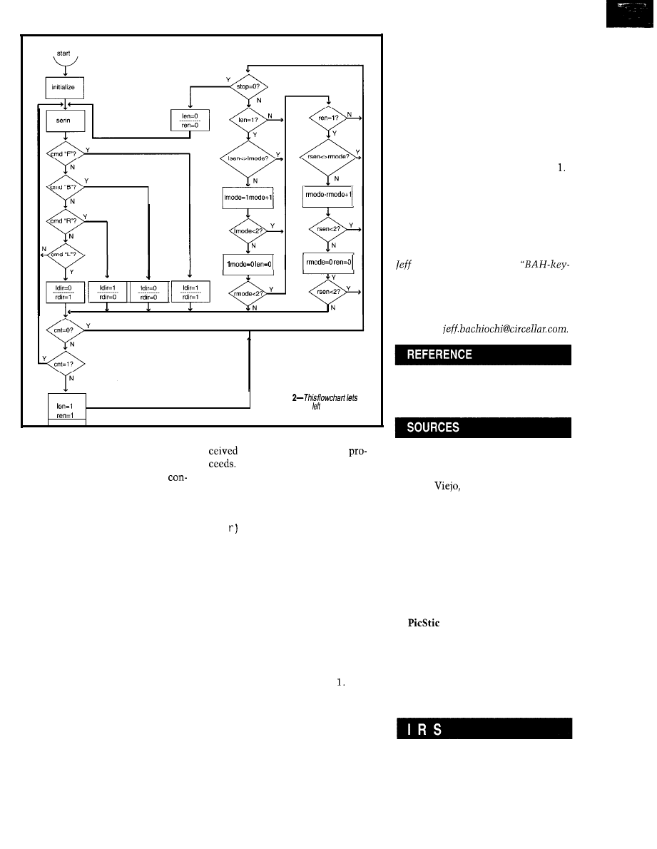
n
dec cnt
Figure
you
trace how the and right motors
operate for the four commands.
wheel at the lever’s end fit perfectly
before the serial routine
between the gears’ teeth.
The switch has about 1 ms of
Two characters are expected after
tact bounce. A bit of external circuitry
the qualified-the command and the
could cure this problem (a fast micro
would see the bounce as multiple
counts). Instead, my code pauses briefly
Control is simplest if you enable
the motors and keep them in step by
whenever the switch changes states.
monitoring the left and right tread
counts. If the counts don’t stay equal,
it temporarily disables one motor.
To move straight, the micro enables
both motors for a specific number of
counts. To stop it before it finishes a
move, use an emergency stop input.
FLOW CARTOGRAPHY
As Figure 2 shows, the software is
simple, using only about 60 commands.
Once the processor is initialized, it
jogs the left and right treads, setting
the position sensors to a known state.
It then waits for serial input.
M
(for
motor) is a qualifier that must be re-
count. Based on the command, the left
and right direction flags (1
d i
r
and
Now, we’re ready to move. If the
count received with the command is 0,
r d
i
are set to 1 for forward and 0 for
then counter decrementing is avoided
reverse movement.
and the control loop (moving each tread
one sensor count) executes continu-
ously until the emergency stop input
is pulled low. The control loop is then
exited, and it waits for serial input.
If the count anything other than 0,
it decrements each time through the
control loop until it reaches At that
time, the loop is again exited to await
another command.
The control loop enables the motor
drivers for both treads. It then enters
an inner loop that alternately checks
each tread’s sensors for changes of
state.
When each tread completes a move
or step, it is disabled until the other
tread catches up. (I hope this will keep
the Dozer from veering off course.]
Once both treads move, the loop exits
and the count is decremented.
SIMPLY BASIC
It
shouldn’t be tough to convince
you just how easily this platform is
programmed. Take a look at Listing
It takes -100 counts to do a 360”
turn. The commands can come from
your keyboard via terminal software.
But, what now? The umbilical cord.
Next month, I cut the apron strings.
“Klatu Barata Nikto!”
q
Bachiochi (pronounced
AH-key”) is an electrical engineer on
Circuit Cellar INK’s engineering staff.
His background includes product
design and manufacturing. He may be
reached at
For more information on National’s
LM18293, check their Web site
(www.national.com).
Motorized Power Shovel/Dozer
Tamiya America, Inc.
2 Orion
Aliso
CA 92656
(714) 362-2240
Fax: (714) 362-2250
LM18293 Quad push-pull
1-A drivers
Digi-Key Corp.
701 Brooks Ave. S
Thief Falls, MN 56701-0677
(218) 681-6674
Fax: (218) 681-3380
1
Micromint, Inc.
4 Park St.
Vernon, CT 06066
(860) 871-6170
Fax: (860) 872-2204
www.micromint.com
425 Very Useful
426 Moderately Useful
427 Not Useful
Circuit Cellar INK@
Issue 93 June 1997
77
Tom Cantrell
SHADES OF MICROCODE
High-Velocity DSP
ompelled by the
march of silicon
integration, computer
architects are doing their
best to find a way through a maze of
rocks and hard places.
Instruction-level parallelism-how
much there is, how to find it, and how
to exploit it-is a key area of interest.
Another is the chip-level equivalent of
convergence, blurring the distinction
between
processing data and those
processing signals (see M.R. Smith’s
“To DSP Or Not To DSP,”
28).
For the most part, microprocessor
gurus have had a pretty easy go of it.
They’ve gotten away with brute forcing
(thanks to nearly free transistors) more
mileage out of old mainframe ideas.
The modern generation of pipelined,
superscalar, speculative
is the result.
But now, other than boosting clock
rate and on-chip cache/memory size,
it’s getting tough to squeeze more
MIPS out of evolutionary designs.
Pressure is building for an architectural
paradigm shift.
Meanwhile, as computers take on
the challenges of multimedia, design-
ers look for solutions with the optimal
combination of data and signal pro-
cessing. Perhaps the time is right to
take a closer look at one of the newer
concepts-VLIW (Very Long Instruc-
tion Word).
A number of chips have toyed with
the idea, but so far, it’s remained little
more than a lab curiosity. Now, the
concept is getting a big push from TI
in the form of their new
series of
featuring a VLIW architecture
they call
Like most ideas in computing, VLIW
isn’t brand new. It’s just newer than
most of the rest.
The original concepts
back
to the days of microcode (remember
how
used to work?). The chal-
lenge is to transform vertical microcode
into a faster horizontal format with
separate fields for each functional unit.
Hennessy and Patterson relate
the early history of VLIW as embodied
in research and commercial machines
such as those offered by Floating Point
Systems, Cydrome, Multiflow, and
companies you’ve likely never heard of.
The reason you’ve never heard of
them is that these machines, and other
’80s vintage
with VLIW-esque
features (e.g., the Intel ‘860 and experi-
mental MIPS prototypes), never ob-
tained much commercial success.
Some argue this proves the VLIW
concept is just another example of a
bad idea whose time has come, but I
suspect it’s not that simple. Perhaps a
combination of at-the-time immature
and constrained technology along with
the end of the Cold War (sapping the
market for performance-at-any-price
crunchers) was more to blame.
While main CPU architects remain
skeptical, the VLIW approach has found
favor in the niche of chips known as
multimedia accelerators from the likes
of Chromatic and Trimedia. Though
the jury is still out, these chips seem
well on their way to rehabilitating the
VLIW concept. Needless to say, the
latest blessing from TI is both signifi-
cant and timely.
MISSION IMPOSSIBLE
That old joke about RISC standing
for Relegate the Impossible Stuff to the
Compiler might better be said about
From high altitude, the problem is
rather simple. The goal: execute as
many instructions per clock as possible.
78
Issue 83
June 1997
Circuit Cellar INK@
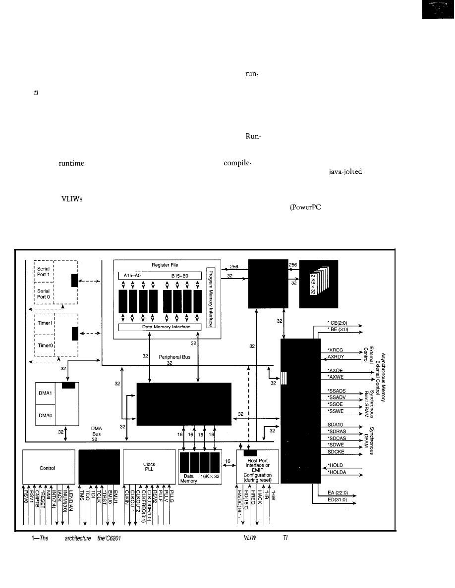
So, CPU operations are scheduled to
fully exploit opportunities for parallel
operation.
Unfortunately, a variety of depen-
dencies and constraints get in the way.
For instance, you can’t read a variable
before it’s written, and you can’t de-
mand functional units when the chip
o n l y h a s n - 1 .
How best to schedule instructions
subject to these constraints is where
the arguments arise. Conventional
superscalar CPU wisdom calls for a
bunch of complex, ugly hardware to
dynamically examine and reorder
instructions at
The good news
is such a chip can handle old binaries,
although a recompile is usually neces-
sary for top performance.
By contrast,
rely on static, or
compile-time, scheduling to organize
instructions most efficiently ahead of
time. Instructions that can execute in
parallel are lined up arm to arm for
digestion by the multiple functional
units in one big gulp.
Reasonable observers can disagree
on whether scheduling dynamically
(hardware) or statically (compiler)
makes more sense. For instance,
time hardware can adapt to conditional
branch behavior, but a static scheme
must commit one way or the other.
On the other hand, dynamic sched-
uling can only deal with a small win-
dow of instructions. Static scheduling
can examine the entire program.
time optimization incurs a silicon
penalty for each chip shipped, whereas
static schemes only pay a
time penalty, presuming such a com-
plex compiler can get beyond beta.
In fact, the overall trend seems to be
to combine the two schemes. By mak-
ing both the chip and compiler smarter,
we can let each do what it does best.
One key question keeps popping up.
Just how much instruction-level paral-
lelism (ILP) is to be found? The answer:
It depends.
For example, Hennessy and Patter-
son examined traces of SPEC92 bench-
marks and found large amounts of ILP
(17.9-150.1 instructions per cycle).
However, since this is based on hind-
sight (actual program traces), it models
a perfect machine with its infinite
resources (registers and function units).
It has foolproof branch prediction
and a full program-size reorder buffer.
Also, it has no aliases, referring to the
situation, as with a C pointer, where
it’s next to impossible to determine if
a data dependency exists.
Even the most
architect
knows such a machine is a look-ahead
pipedream. Hennessy and Patterson
perform a similar analysis with a real
CPU
620). Although it’s
theoretically capable of issuing 4 in-
structions per cycle, it barely averages
1.3.
Ouch!
Figure
radical
of
represents a major blessing of-and commitment to-the
concept by
Circuit Cellar INK@
Issue 83 June 1997
7 9
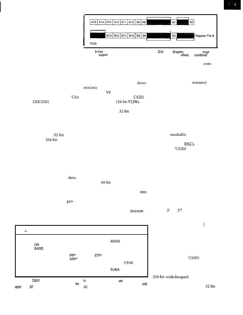
However, one key point (and hope)
to note is that different kinds of pro-
grams exhibit more or less ILP. In
particular, vector loops (e.g., vector
add, dot product, etc.) are relatively
more parallelizable, and such routines
are at the core of signal processing.
I’ve spent a lot of time up front
looking at the big picture in the hope
of making the motivation behind VLIW
a little easier to understand. Needless
to say, the TI chips aren’t your father’s
CPU.
V8 PUNCH
“There’s no substitute for cubic
inches” is a hot-rodder maxim that
applies well to the first chip in the
series-the
The chip com-
bines a whopping 8 functional units
with 1 Mb of on-chip zero-wait-state
SRAM and a bunch of glue logic, all
running at up to 200 MHz (see Figure 1).
Featuring the silicon equivalent of
multiport fuel injection, each func-
tional unit gets its own
fetch
bus. It makes for a
“instruc-
tion,” which is what the VL in VLIW
is all about.
The on-chip SRAM is split in half,
with 2k 256-bit instructions joined by
16 K x 32 data RAM. The instruction
memory can be reconfigured to operate
as a direct-mapped cache.
SIMD-like partitioning of the
memory interface enables simultaneous
transactions to different banks. Regis-
ters and off-chip data memory are all
Register File A
Registers used for
circular addressina
Registers tested
for condition
Registers used with
offset addressing
Figure
cluster has a complement of 16
Kx
registers.
are genera/ purpose!
certain ones
alternative functions, including circular addressing, long branch
and
execution.
Note that switching the program
branches based on PSW flags is
RAM from memory to cache mode
pletely discarded.
invalidates the cache. However, it is
Instead, the CPU has conditional
possible to freeze the cache anytime,
execution for every instruction based
locking the contents for fast and
on the contents (zero or
of
access.
Much as a is conceptually two
straight-4s stuck together, the
is actually a pair of
Each has four function units, 16 K x
32-bit registers, and a
data bus.
Like a crankshaft, cross paths link
clusters, enabling function units on one
side to access registers on the other.
Similarly, a register on one side gener-
ates an address for loads/stores on the
other.
As shown in Table 1, each function
unit is responsible for part of the in-
struction set. It’s an interesting hybrid
of three-operand load/store RISC spiced
up with DSP features.
The latter includes circular address-
ing (i.e., software FIFO), saturated math
(results top and bottom out, rather than
overflow),
calculation headroom
[using a pair of registers), and so on.
Barrel shifters support a variety of
byte, half-word, and word addressable.
clock bit field operations, including
It’s possible to store into the
shifts, searches, and extracts.
gram memory 32 bits at a time with
Other features not particularly
the STP instruction. But, there’s no
related to DSP functions are
way [and since it’s RAM, no need) to
ing nonetheless. For instance, the
load from program memory.
traditional concept of conditional
Unit
.M Unit
.S Unit
.D Unit
ABS
NORM
MPY
ADD
EXT
SET
ADD
ADD
MPT
SMPY
ADDK
EXTU
SHL
AND
C M P E Q
ADD2
MVC*
SHR
LD mem
AND MV
SHRU
LD mem (15-bit offset)**
C M P G T S A T
B disp MVK
SSHL MV
CMPGTU SSUB
B
MVKH
NEG
C M P L T S U B
B
N E G
SUB
ST mem
CMPLTU SUBC
B reg
NOT
SUB2
ST mem
offset)**
LMBD
XOR
CLR OR
XOR
SUB
MV
XOR
ZERO
NEG
ZERO
Table l--The
relies on four types of functional units handle fhe entire instruction
Two such groups
(each sometimes referred to as a “cluster”) compose
total of eight function units. Sing/e-asterisk instructions
to the
components, and double asterisks apply to
80
Issue
83 June 1997
Circuit Cellar INK@
certain registers. This works in concert
with CMP instructions that compare
two source registers and put a 0 or 1 in
a destination register accordingly.
Thus, there aren’t any conditional
branch (B) instructions per se. But like
any other instruction, branches can be
made conditional. Besides the expected
register and displacement options, the
B I R P and B N R P variants act as re-
turns from
and nonmaskable
interrupts, respectively.
Like some other
(MIPS comes
to mind), the
does little in
response to interrupts except store the
return address one-level deep on chip
and mask further interrupts. Any nest-
ing, dynamic priority, or other fancy
interrupt pretensions are left com-
pletely up to software.
As you see in Figure 2, other regis-
ters play special roles for circular ad-
dressing and long (15 vs. 5 bit) offset
addressing. Circular addressing mode
is enabled with a control register that
also specifies block size (powers of two
between and bytes).
Subsequently, add and subtract
operations on the affected registers
(whether via an explicit ADD and U B
or a load/store address increment and
decrement) are calculated in a modulo
manner (i.e., they wrap around once
the block size is exceeded).
NOP IN
MY BACKYARD
Table 2 shows the
“pipe-
line,” though that term is a bit mis-
leading.
The front of the pipeline is a single
that grabs fetch
packets from memory. In the middle,
the long fetch packet splits into
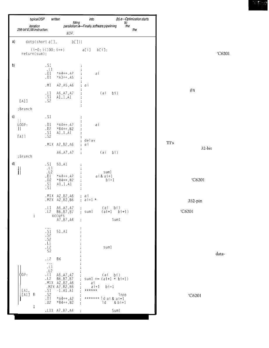
Listing 1 a-A
loop
in C
translates easily
serial assembler
by scheduling around resource constraints and
delay slots. d-The loop is unrolled hand/e two array
elements per
and expose more
packs entire loop info
one
The asterisks show how each unit works on a different iteration of
loop,
eliminating dependencies and every sing/e
int
short
int sum = 0, i;
for
sum +=
*
MVK
100, Al
ZERO
A7
LOOP:
LDH
LDH
NOP 4
MPY
NOP
ADD
SUB
B
LOOP
NOP 5
occurs here
MVK
100, Al
ZERO .Ll A7
LDH
LDH
SUB
B
LOOP
NOP 2
MPY
NOP
ADD .Ll
occurs here
MVK
ZERO
A7
ZERO
B7
LOOP:
LDW
LDW
SUB
B
LOOP
NOP 2
MPY
MPYH
NOP
ADD
ADD
Branch
ADD .LIX
B
s2
MVK
B
B
ZERO
ZERO
B
ZERO :Ll
ZERO
here
LOOP
LOOP
LOOP
A7
B7
LOOP
A6
B
s2
LOOP
ZERO
A2
ZERO
B2
ADD
ADD
MPY
MPYH
1 ADD
L O O P
LDW
LDW
Branch occurs here
ADD
set up loop counter
zero out accumulator
load from memory
load bi from memory
delay slots for LDH
* bi
delay slot for MPY
sum +=
*
decrement loop counter
branch to loop
delay slots for branch
set up loop counter
zero out accumulator
load from memory
load bi from memory
decrement loop counter
branch to loop
slots for LDH
* bi
delay slots for mpy
sum +=
*
set up loop counter
zero out sum0 accumulator
zero out
accumulator
load
from memory
load bi &
from memory
decrement loop counter
branch to loop
* bi
bi+l
sum0 +=
*
+=
*
sum = sum0 +
branch to loop
set up loop counter
* branch to loop
** branch to loop
zero out sum0 accumulator
zero out
accumulator
*** branch to loop
zero out ADD input
zero out ADD input
**** branch to loop
zero out MPY input
zero out MPY input
sum0 +=
*
** * bi
**
*
decrement loop counter
***** branch to
fm memory
******* bi
fm memory
sum = sum0 +
execute
packets for dispatch to each
functional unit.
Each single-stage functional unit
then requires a particular number of
cycles depending on the operation (i.e.,
one for simple ALU ops, two for multi-
plies, five for loads, six for branches).
Rather than interlocks, the
relies on delay slots to handle the vary
ing cycle count in the execution stage.
The compiler tries to find useful in-
structions to fill the void, but it’s tough
to do. Sometimes, the only choice is to
kill time with NO
Ps.
To this end, TI
includes a
NOP
(n = 1
to
9)
instruc-
tion to prevent needless duplication.
Along similar lines, concerns about
VLIW code density have been made.
After all, if the machine only delivers
“a few” instructions per cycle on real
programs, then there are “8 minus a
few” N 0
Ps
in baggage. Memory may be
cheap, but it’s not cheap enough to
throw half or more away.
solution is to make the least
significant bit of each
instruction
a parallel bit. If it’s 1, the next instruc-
tion in the fetch packet is added to the
current execute packet. If 0, the next
instruction goes into the following
execute packet.
All in all, the
goes a long
way in placating the N 0
P
naysayers.
MOTOR MOUNTS
Though the
ball grid array
(BGA) package may make you fear the
worst, the
glue logic pretty
much insulates the system designer
from the on-chip complexity. Actually,
about half the pins are devoted to the
dual power supply, comprising 2.5 V
for internal operation and 3.3 V for I/O.
To date, final production device
power hasn’t been characterized. But
given the clock rate and wide
paths, a half dozen or so watts won’t
be a surprise.
The chip has the increasingly stan-
dard triad of power-reduction modes
that stop the CPU, I/O, or both. They
trade off less stand-by power for fewer
wake-up options.
Making the
an easy drop-in
starts with a clock generator featuring
a programmable 1:
1, 2:
1, or
4:
1 PLL. So,
the clock source is limited to 50 MHz,
cutting design and FCC hassles.
Circuit Cellar INK@
Issue 83 June 1997
8 3
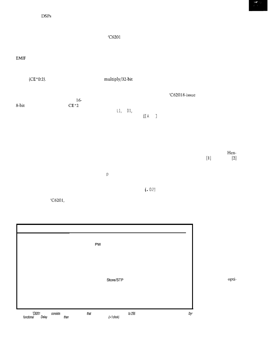
Like many
with on-chip pro-
gram RAM, a built-in DMA controller
handles bootloading from external
memory, which can be slow and/or
narrow (e.g., x8 EPROM). It also takes
care of user-defined data-transfer chores.
The CPU and DMAC both get ac-
cess to external memory through the
(External Memory Interface). It
features 23 address lines and 32 data
lines coupled with individual byte
enable lines (BE*O-3) and three chip
selects
All three chip-select spaces support
32-bit data width and asynchronous
(i.e., EPROM, SRAM) memory. As
well, CE* 1 can be configured for
or
width, while CE*O and
can
operate in high-speed burst SRAM and
synchronous DRAM modes.
Finally, a dedicated port is provided
for access by a host CPU. Having as-
serted Host Request (HREQ) and re-
ceived Host Acknowledge [HACK), it
can access the on-chip memory using
16-bit address and data buses with read
and write strobes.
Note the protocol asks for a degree
of cooperation from each party. The
host isn’t granted access until all pend-
ing on-chip data-memory accesses
cease. But once the host has control, it
can keep it indefinitely, locking out
the on-chip CPU and DMAC.
A few additions are planned to the
first version of the
including
dual serial ports and timers (shown in
dotted lines in Figure 1). Also, some
existing functions (e.g., the SDRAM
interface and memory-map options]
will be improved.
HIGH-OCTANE SOFTWARE
If the
is the motor, then your
software is the fuel. You need the good
stuff to avoid NOP knock. Remember
the basic premise of VLIW is that you
and the compiler not only get to-but
must-generate optimal code.
For an idea of what’s involved, look
at Listing la. It shows a classic vector
16-bit
accumulate loop
(dot product) written in C, similar to
the inner loops of many DSP applica-
tions. Listing lb shows the same loop
translated to serial assembly language.
Except for the functional unit desig-
nations (e.g., . . . Ml, etc.) and
conditional execution feature
1
makes the branch conditional), the code
is similar to what you find on a conven-
tional RISC with delay slots. And, just
as on that RISC, the next step is to
schedule around resource (functional
unit, register, and bus] constraints and
to fill delay slots as shown in Listing lc.
The parallel bars in the first column
indicate the instruction can execute in
parallel with the previous one (i.e., the
opcode bit described earlier). The first
two instructions, using different units,
parallelize easily.
Notice how a second unit
is
allocated to allow the two LDH instruc-
tions to proceed. Instructions are also
moved around to fill delay slots.
Execution time is cut in half, which
is good, but so far, not much better than
Pipeline Phase
Pipeline Stage
Symbol During this Phase:
Program Fetch
Program Address Generate
PG
Program Address Send
PS
Program Wait
Program Data Receive
PR
Program Decode Execute Packet Dispatch
DP
Decode
DC
Execute
Execute 1
El
Execute 2
Execute 3
Execute 4
Execute 5
E2
E3
E4
E5
The process known as loop unroll-
ing (see Listing Id) isn’t so much about
cutting overhead as exploiting more
parallelism. Here, the inner loop cycle
count remains unchanged. But, there
are only half as many iterations, so
performance doubles again.
It’s definitely interesting, but still
not spectacular. After all, IPC is still
less than 2, a small fraction of the
c a p a b i l i t y .
But now, the fun begins. The pre-
mise of VLIW proponents is that, with
full program visibility and explicit
knowledge of and control over machine
resources, much more aggressive opti-
mization is possible.
Research has centered on advanced
techniques like memory disambiguation
(to get
around the dependency-inducing
alias problem) and trace scheduling (to
move code across basic blocks).
nessy and Patterson and others
describe these techniques in gory detail.
One key optimization-software
pipelining-is especially useful for
tight vector loops. The concept is, like
a hardware pipeline, rather simple in
principle if not in practice. The goal is
simply to start a new iteration of the
loop as soon as possible.
Evaluating resource and dependency
constraints determines the minimum
iteration interval (i.e., the minimum
number of cycles be-
tween iterations). So,
the code breaks up into
a prologue (i.e., prime
the pipeline) and epi-
logue (i.e., drain it)
surrounding a fully
parallel inner loop.
Turns out, the very
fastest schedule can
bloat code size a lot.
But, subsequent
mizations (e.g., extra-
neous load removal
and prologue and epi-
logue reduction] cut
size significantly with
Address of the fetch packet is determined
Address of the fetch packet is sent to memory
Program memory read is performed
Fetch packet is expected at CPU boundary
Next execute packet is sent to functional units
Instructions are decoded in functional units
Instruction conditions are evaluated, operands read
Load/store addresses are computed/modified
Branches affect fetch packet in PG stage
Single-cycle results are written to register file
Load address is sent to memory
address and data are sent to memory
Single-cycle instructions can set SAT bit
Multiply results are written to register file
Load memory reads continue
Multicycle instruction can set SAT bit
Load data arrives at CPU boundary
Load data is placed in register
what you’d find on a run-of-the-mill
CPU. One simple optimization: use
LDW (32 bit) instead of LDH (16 bit)
and work on two elements of each
array at a time.
only a minor reduction
Table 2-The
pipeline
of a sing/e front-end fetches and cracks long (up
bit) instructions into pieces for execution
each
unit.
slots, rather
interlocks, accommodate slow
operations, including multiplies, loads, and branches.
(-10%) in speed.
84
Issue
83 June
1997
Circuit Cellar INK@
To make a long story short, Listing
le shows a code-efficient
pipelined version of the dot-product
example. You may need more than a
few moments to decipher it, but the
point is that the entire loop has
been parallelized into a single cycle
instruction with all cylinders
firing for a nearly 8x
COMPILER
That’s impressive. Compared to the
unoptimized serial assembly, the final
version speeds up the overall routine
by a factor of -25, only slightly derated
(due to epilogue and prologue) from the
inner-loop
of 32x.
Yes, the chip may seem expensive
($96 at
But, what if it can handle
IO-15 modems in software compared
to one for a $10 DSP?
There’s certainly nothing wrong
with hand coding and tuning your appli-
cation’s critical loops. Indeed, doing
anything less invariably leaves many
MIPS on the table. However, there’s
also no doubt all the head scratching
gets old quick.
The million-dollar question: will
the TI tools, including the optimizing
assembler that schedules delay slots
and allocates registers, the C compiler
that features global (i.e., entire pro-
gram) scope, and the
lining optimizations ($2495 for the C
and ASM combo for Windows
not to mention the JTAG-based debug-
ging scheme, live up to the promise?
My guess is the combination of
smarter tools, libraries of hand opti-
mized code, and continuing march of
silicon (notably large and wide on-chip
memory), combined with the demand
for more media savvy applications and
the blessing of a heavy hitter like TI,
may mean
time has finally
come.
q
Tom
has been working on
chip, board, and systems design and
marketing in Silicon Valley for more
than ten years. He may be reached by
E-mail at
by telephone at (510)
or by
fax at (510)
J. Hennessy and D. Patterson,
Computer Architecture: A
Quantitative Approach,
2nd
Ed., Morgan Kaufmann Publish-
ers, 1996.
J. Ellis,
Bulldog: A Compiler for
VLIW Architectures,
The MIT
Press, 1986.
series, Programmers Guide
SPRU198
Texas Instruments, Inc.
Semiconductor Gr. SC-97001A
Literature Response Ctr.
P.O. Box 172228
Denver, CO 80217
(800) 477-8924, x4500
Fax: (303) 294-3738
428 Very Useful
429 Moderately Useful
430 Not Useful
Professional, high-performance real-
time
for DOS
and
Embedded Systems.
For
Borland UC++,
UC++. and Borland
Libraries: $550 Source Code: add $500
Cross
S
for 32-bit Embedded
stem
ystems.
386
little
for Borland UC++,
C/C++, and
C/C++.
Libraries:
Source Code: add I
2
Professional, high-performance real-
time multitasking system
for 32-bit
Embedded Systems.
Supports
386 and higher.
for
B o r l a n d U C + + ,
U C + + , a n d
U C + + .
Libraries:
Source Code: add 650
America, please contact:
Other Countries:
O n
Phone
l
l
l
and lists
Circuit Cellar INK@
Issue 83 June 1997
85
INTERRUPT
A Winning Proposition
he editorial direction of Circuit
primarily an extension of my own technical interests. It’s a lime line of
subjects that started 19 years ago at
continues today. Of course, if you look back at those early projects
now, you might come away with the impression that specialized in presenting some realty off-the-wall computing
concepts. Back then, these articles were considered state-of-the-art, assure you.
Today, Circuit Cellar
to focus on computer applications, but as you might expect, the technical level of the presentation has
grown considerably. The reason is because I base our delivery level on an ever-increasing standard built on accumulated experience and
expanding knowledge. We don’t rehash the same stuff and periodically count on a new generation of readers to present the same documenta-
tion to over and over. When a simple
is the preferred parallel interface, that’s what we write about. When accepted practice becomes a
custom-programmed coprocessor instead, that’s the way we present it.
This is not an easy balance. Often, you’re damned if you do and damned if you don’t. Just like job applicants finding potential employers
who applaud their cross-technology training but won’t hire them because their degree isn’t specific enough, we find advertisers who applaud our
embedded focus but are tough to sign because their specific product category isn’t in the magazine’s name. If we published
World,
Emulator Action News,
or
Tools Monthly, it would be easy.
When we started the Embedded
to acknowledge that the 80x86 architecture was a viable application alternative, I removed a
major obstacle to many who didn’t understand our broader focus. You and know it’s just the next step in the accumulated experience base
called “embedded control.” But to them, it’s like waving a flag with an identifiable product category on it. Not only did they become advertisers,
but when we sought support for an Embedded PC contest, we had to stand aside so as not to get trampled in the rush. That’s how we got 17
sponsors and almost $11,000 in prize money.
Does this mean I plan to change the magazine into an embedded-PC manifest? Hell, no!
The massive support for an embedded-PC contest is the result of having a specific product focus identifiable to specific sponsors.
Whenever I’ve presented a design contest in the past, it has had a general focus aimed at a general group of potential sponsors and with a
general objective. There’s a message there someplace.
The reality is that a successful general design contest has to have either a specific focus or specific sponsors. I know this sounds
ridiculous. Making it specific seems to take it out of the “general” category, doesn’t it? While the purists among you might fight my logic, I find
that necessity promotes compromise. While a general contest certainly shouldn’t have a specific focus, there’s no reason a general contest can’t
have a specific sponsor with a general product line.
At this writing, we are negotiating with a major semiconductor manufacturer to sponsor a spring 1998 Circuit Cellar Design Contest. With
their support, it is our intention that the prizes and promotion will be equivalent to
present Embedded PC Design Contest. I can’t give you
any details until they sign on the dotted line, but my objective is to have a contest that provides a wide option for technical solutions and various
levels of application expertise.
Ultimately, it’s reader support that still makes it a pleasure to plan and direct Circuit Cellar. I’m sure our parallel destinies --INK’s and my
own-will take us where we’d never have gone alone. But rest assured, any moves we make will only and always be in response to you. We will
stay your course.
P.S.: Speaking of the Embedded PC Design Contest, the deadline for submissions has been extended from August 1st until September 1st by
popular demand. For any notices or information about the contest, see our Web site at
96
Circuit Cellar INK@
Wyszukiwarka
Podobne podstrony:
circuit cellar1995 06
circuit cellar2001 06
circuit cellar1996 06
circuit cellar2002 06
circuit cellar1993 06
circuit cellar1994 06
circuit cellar1991 06,07
circuit cellar1992 06,07
circuit cellar2004 06
circuit cellar2003 06
circuit cellar1990 06,07
circuit cellar1995 06
circuit cellar2001 06
circuit cellar1991 06,07
circuit cellar1993 06
circuit cellar1996 06
więcej podobnych podstron