HCC/HCF4027B
DUAL-J-K MASTER-SLAVE FLIP-FLOP
DESCRIPTION
.
SET-RESET CAPABILITY
.
STATIC FLIP-FLOP OPERATION - RETAINS
STATE INDEFINITELY WITH CLOCK LEVEL
EITHER ”HIGH” OR ”LOW”
.
MEDIUM SPEED OPERATION - 16MHz (typ.
clock toggle rate at 10V)
.
STANDARDIZED
SYMMETRICAL
OUTPUT
CHARACTERISTICS
.
QUIESCENT CURRENT SPECIFIED TO 20V
FOR HCC DEVICE
.
INPUT CURRENT OF 100nA AT 18V AND 25
°
C
FOR HCC DEVICE
.
100% TESTED FOR QUIESCENT CURRENT
.
MEETS ALL REQUIREMENTS OF JEDEC TEN-
TATIVE STANDARD N
0
. 13A, ”STANDARD
SPECIFICATIONS FOR DESCRIPTION OF ”B”
SERIES CMOS DEVICES”.
June 1989
The HCC4027B (extended temperature range) and
HCF4027B (intermediate temperature range) are
monolithic integrated circuit, available in 16-lead
dual in-line plastic or ceramic package and plastic
micro package.
The HCC/HCF4027B is a single monolithic chip in-
tegrated circuit containing two identical complemen-
tary-symmetry J-K master-slave flip-flops. Each
flip-flop has provisions for individual J, K, Set, Reset,
and Clock input signals, Buffered Q and Q signals
are provided as outputs. This input-output arrange-
ment provides for compatible operation with the
HCC/HCF4013B dual D-type flip-flop.
The HCC/HCF4027B is useful in performing control,
register, and toggle functions. Logic levels present
at the J and K inputs along with internal self-steering
control the state of each flip-flop ; changes in the flip-
flop state are synchronous with the positive-going
transition of the clock pulse. Set and reset functions
are independent of the clock and are initiated when
a high level signal is present at either the Set or
Reset input.
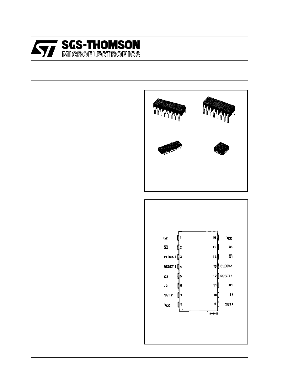
EY
(Plastic Package)
F
(Ceramic Frit Seal Package)
ORDER CODES :
HCC4027BF
HCF4027BM1
HCF4027BEY
HCF4027BC1
PIN CONNECTIONS
M1
(Micro Package)
C1
(Plastic Chip Carrier)
1/12
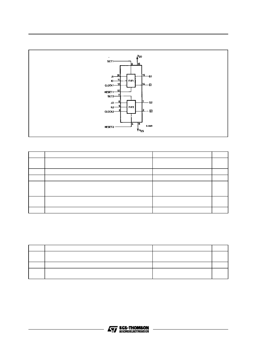
FUNCTIONAL DIAGRAM
ABSOLUTE MAXIMUM RATINGS
Symbol
Parameter
Value
Unit
V
DD
*
Supply Voltage : HCC Types
HC F Types
– 0.5 to + 20
– 0.5 to + 18
V
V
V
i
Input Voltage
– 0.5 to V
DD
+ 0.5
V
I
I
DC Input Current (any one input)
±
10
mA
P
t o t
Total Power Dissipation (per package)
Dissipation per Output Transistor
for T
o p
= Full Package-temperature Range
200
100
mW
mW
T
o p
Operating Temperature : HCC Types
H CF Types
– 55 to + 125
– 40 to + 85
°
C
°
C
T
s t g
Storage Temperature
– 65 to + 150
°
C
RECOMMENDED OPERATING CONDITIONS
Symbol
Parameter
Value
Unit
V
DD
Supply Voltage : HCC Types
HC F Types
3 to 18
3 to 15
V
V
V
I
Input Voltage
0 to V
DD
V
T
o p
Operating Temperature : HCC Types
H CF Types
– 55 to + 125
– 40 to + 85
°
C
°
C
Stresses above those listed under ”Absolute Maximum Ratings” may cause permanent damage to the device. This is a stress rating only
and functional operation of the device at these or any other conditions above those indicated in the operational sections of this specification
is not implied. Exposure to absolute maximum rating conditions for external periods may affect device reliability.
* All voltage values are referred to V
SS
pin voltage .
HCC/HCF4027B
2/12
LOGIC DIAGRAM AND TRUTH TABLE
Present State
Next State
Inputs
Output
CL
∆
Outputs
J
K
S
R
Q
Q
Q
I
X
O
O
O
–
/
–
I
O
X
O
O
O
I
–
/
–
I
O
O
X
O
O
O
–
/
–
O
I
X
I
O
O
I
–
/
–
O
I
X
X
O
O
X
–
\–
←
No Change
X
X
I
O
X
X
I
O
X
X
O
I
X
X
O
I
X
X
I
I
X
X
I
I
ONE OF TWO IDENTICAL J-K FLIP-FLOPS
LOGIC I = HIGH LEVEL
LOGIC O = LOW LEVEL
∆
- LEVEL CHANGE
X - DON’T CARE
TRUTH TABLE
HCC/HCF4027B
3/12
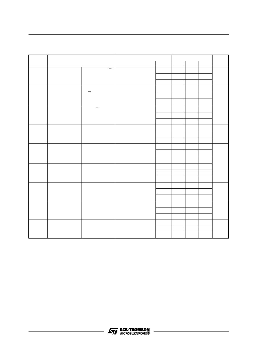
STATIC ELECTRICAL CHARACTERISTICS (over recommended operating conditions)
Test Conditions
Value
V
I
V
O
|I
O
|
V
D D
T
L o w
*
25
°
C
T
Hi g h
*
Symbol
Parameter
(V)
(V)
(
µ
A)
(V)
Min. Max. Min. Typ. Max. Min. Max.
Unit
I
L
Quiescent
Current
HCC
Types
0/ 5
5
1
0.02
1
30
µ
A
0/10
10
2
0.02
2
60
0/15
15
4
0.02
4
120
0/20
20
20
0.04
20
600
HCF
Types
0/ 5
5
4
0.02
4
30
0/10
10
8
0.02
8
60
0/15
15
16
0.02
16
120
V
O H
Output High
Voltage
0/ 5
< 1
5
4.95
4.95
4.95
V
0/10
< 1
10
9.95
9.95
9.95
0/15
< 1
15
14.95
14.95
14.95
V
O L
Output Low
Voltage
5/0
< 1
5
0.05
0.05
0.05
V
10/0
< 1
10
0.05
0.05
0.05
15/0
< 1
15
0.05
0.05
0.05
V
IH
Input High
Voltage
0.5/4.5
< 1
5
3.5
3.5
3.5
V
1/9
< 1
10
7
7
7
1.5/13.5
< 1
15
11
11
11
V
IL
Input Low
Voltage
4.5/0.5
< 1
5
1.5
1.5
1.5
V
9/1
< 1
10
3
3
3
13.5/1.5
< 1
15
4
4
4
I
O H
Output
Drive
Current
HCC
Types
0/ 5
2.5
5
– 2
– 1.6 – 3.2
– 1.15
mA
0/ 5
4.6
5
– 0.64
– 0.51 – 1
– 0.36
0/10
9.5
10
– 1.6
– 1.3 – 2.6
– 0.9
0/15
13.5
15
– 4.2
– 3.4 – 6.8
– 2.4
HCF
Types
0/ 5
2.5
5
– 1.53
– 1.36 – 3.2
– 1.1
0/ 5
4.6
5
– 0.52
– 0.44 – 1
– 0.36
0/10
9.5
10
– 1.3
– 1.1 – 2.6
– 0.9
0/15
13.5
15
– 3.6
– 3.0 – 6.8
– 2.4
I
O L
Output
Sink
Current
HCC
Types
0/ 5
0.4
5
0.64
0.51
1
0.36
mA
0/10
0.5
10
1.6
1.3
2.6
0.9
0/15
1.5
15
4.2
3.4
6.8
2.4
HCF
Types
0/ 5
0.4
5
0.52
0.44
1
0.36
0/10
0.5
10
1.3
1.1
2.6
0.9
0/15
1.5
15
3.6
3.0
6.8
2.4
I
IH
, I
IL
Input
Leakage
Current
HCC
Types
0/18
Any Input
18
±
0.1
±
10
– 5
±
0.1
±
1
µ
A
HCF
Types
0/15
15
±
0.3
±
10
– 5
±
0.3
±
1
C
I
Input Capacitance
Any Input
5
7.5
pF
* T
Low
= – 55
°
C for HCC device : – 40
°
C for HCF device.
* T
High
= + 125
°
C for HCC device : + 85
°
C for HCF device.
The Noise Margin for both ”1” and ”0” level is : 1V min. with V
DD
= 5V, 2V min. with V
DD
= 10V, 2.5 V min. with V
DD
= 15V.
HCC/HCF4027B
4/12
DYNAMIC ELECTRICAL CHARACTERISTICS (T
amb
= 25
°
C, C
L
= 50pF, R
L
= 200k
Ω
,
typical temperature coefficient for all V
DD
= 0.3%/
°
C values, all input rise and fall time = 20ns)
Value
Symbol
Parameter
Test Conditions
V
DD
(V)
Min.
Typ.
Max.
Unit
t
PLH
, t
PHL
Propagation
Delay Time
Clock to Q or Q
Outputs
5
150
300
ns
10
65
130
15
45
90
t
PLH
Propagation
Delay Time
Set to Q or Reset
t o Q
5
150
300
ns
10
65
130
15
45
90
t
PHL
Propagation
Delay Time
Set to Q or Reset
to Q
5
200
400
10
85
170
15
60
120
t
THL
, t
TLH
Transition Time
5
100
200
ns
10
50
100
15
40
80
t
W
Pulse Width
Clock
5
140
70
ns
10
60
30
15
40
20
t
W
Pulse Width
Set or Reset
5
180
90
10
80
40
15
50
25
t
r
,t
f
Clock Input Rise
or Fall Time
5
15
µ
s
10
4
15
1
t
se tu p
Setup Time
Data
5
200
100
ns
10
75
35
15
50
25
f
max
Maximum
Clock Input
Frequency *
Toggle Mode
5
3.5
7
MHz
10
8
16
15
12
24
* Input tr, tf = 5ns.
HCC/HCF4027B
5/12
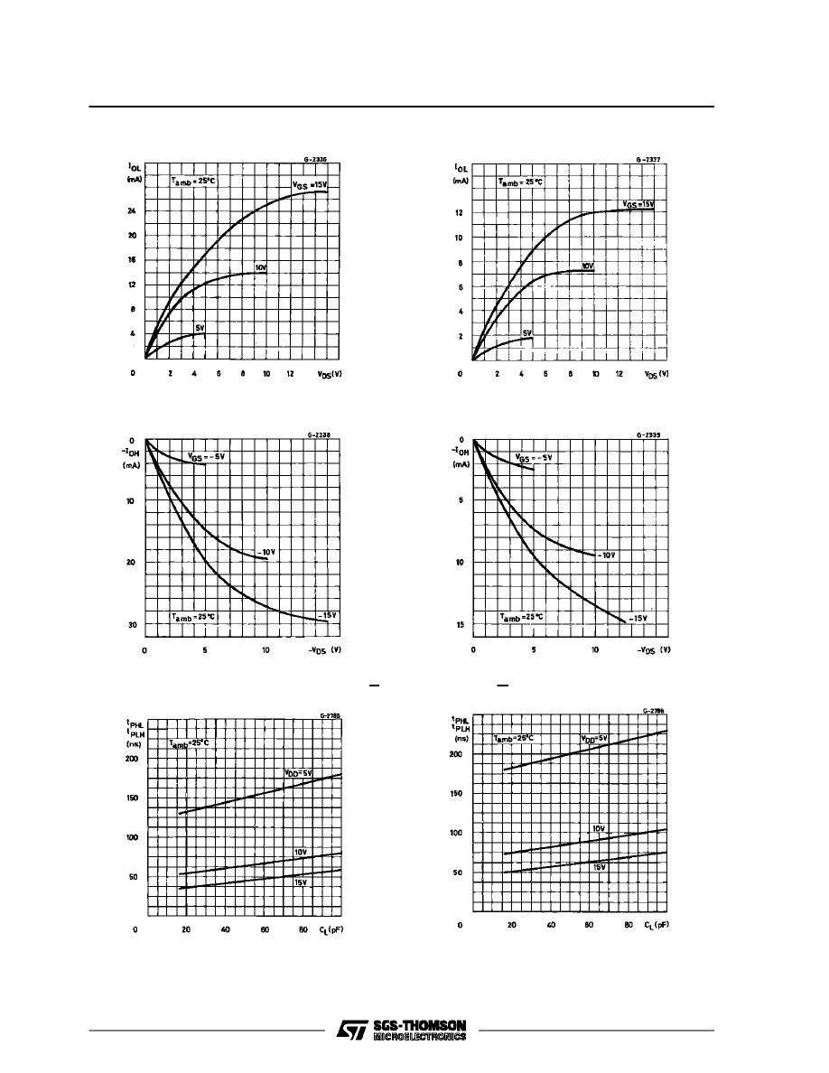
Typical Output Low (sink) Current Characteristics.
Minimum Output Low (sink) Current Characteristics.
Typical Output High (source) Current Charac-
teristics.
Minimum Output High (source) Current Charac-
teristics.
Typical Propagation Delay Time vs. Load Capacit-
ance (SET to Q or RESET to Q).
Typical Propagation Delay Time vs.Load Capacit-
ance (CLOCK or SET to Q, CLOCK or RESET to Q).
HCC/HCF4027B
6/12
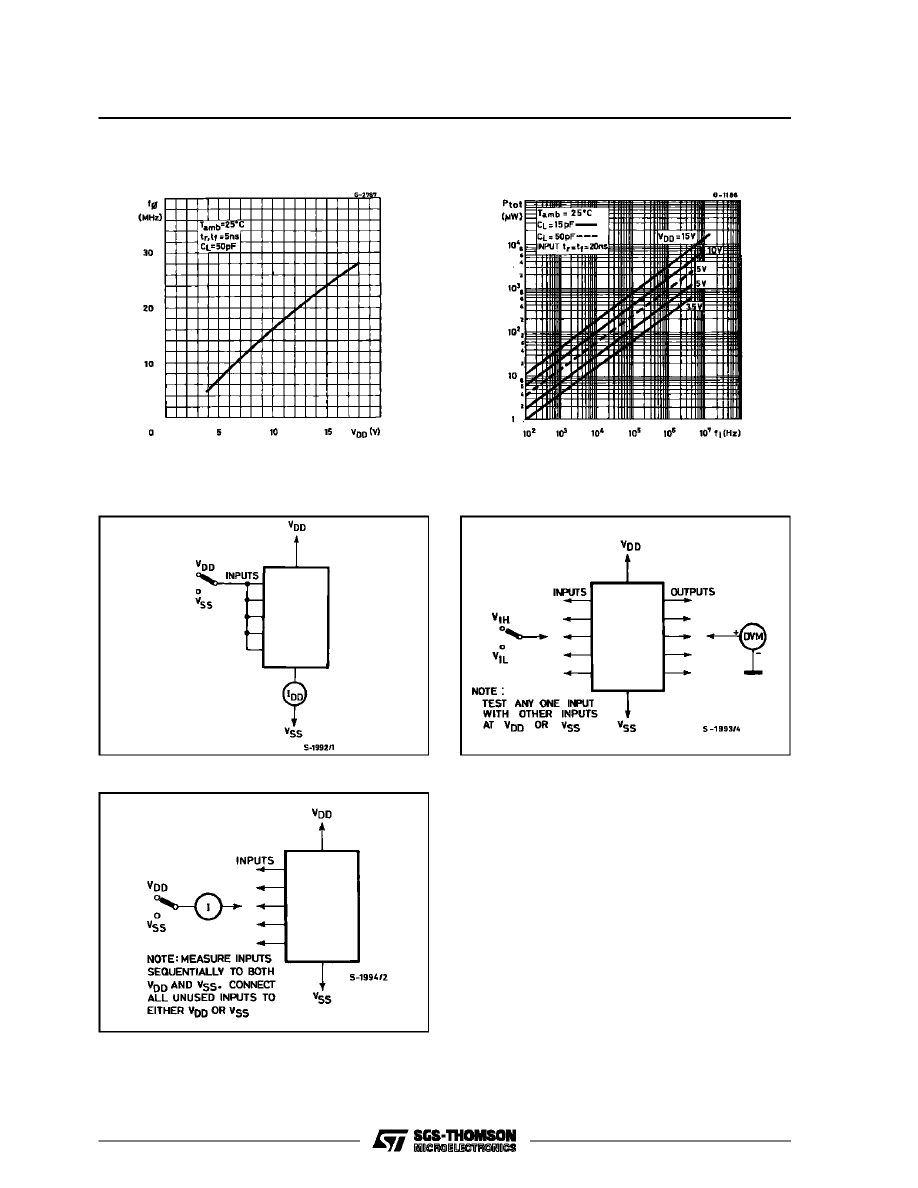
Typical Maximum Clock Frequency vs. Supply
Voltage (Toggle Mode).
Typical Dynamic Power Dissipation/ Per Device
vs.Frequency.
Input Leakage Current.
Input Voltage.
TEST CIRCUITS
Quiescent Device Current.
HCC/HCF4027B
7/12
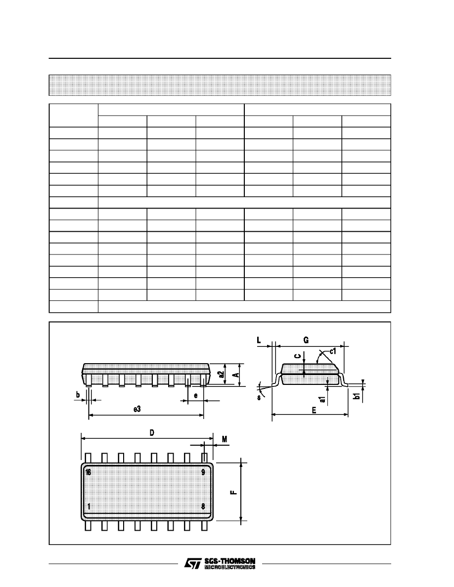
Plastic DIP16 (0.25) MECHANICAL DATA
DIM.
mm
inch
MIN.
TYP.
MAX.
MIN.
TYP.
MAX.
a1
0.51
0.020
B
0.77
1.65
0.030
0.065
b
0.5
0.020
b1
0.25
0.010
D
20
0.787
E
8.5
0.335
e
2.54
0.100
e3
17.78
0.700
F
7.1
0.280
I
5.1
0.201
L
3.3
0.130
Z
1.27
0.050
P001C
HCC/HCF4027B
8/12
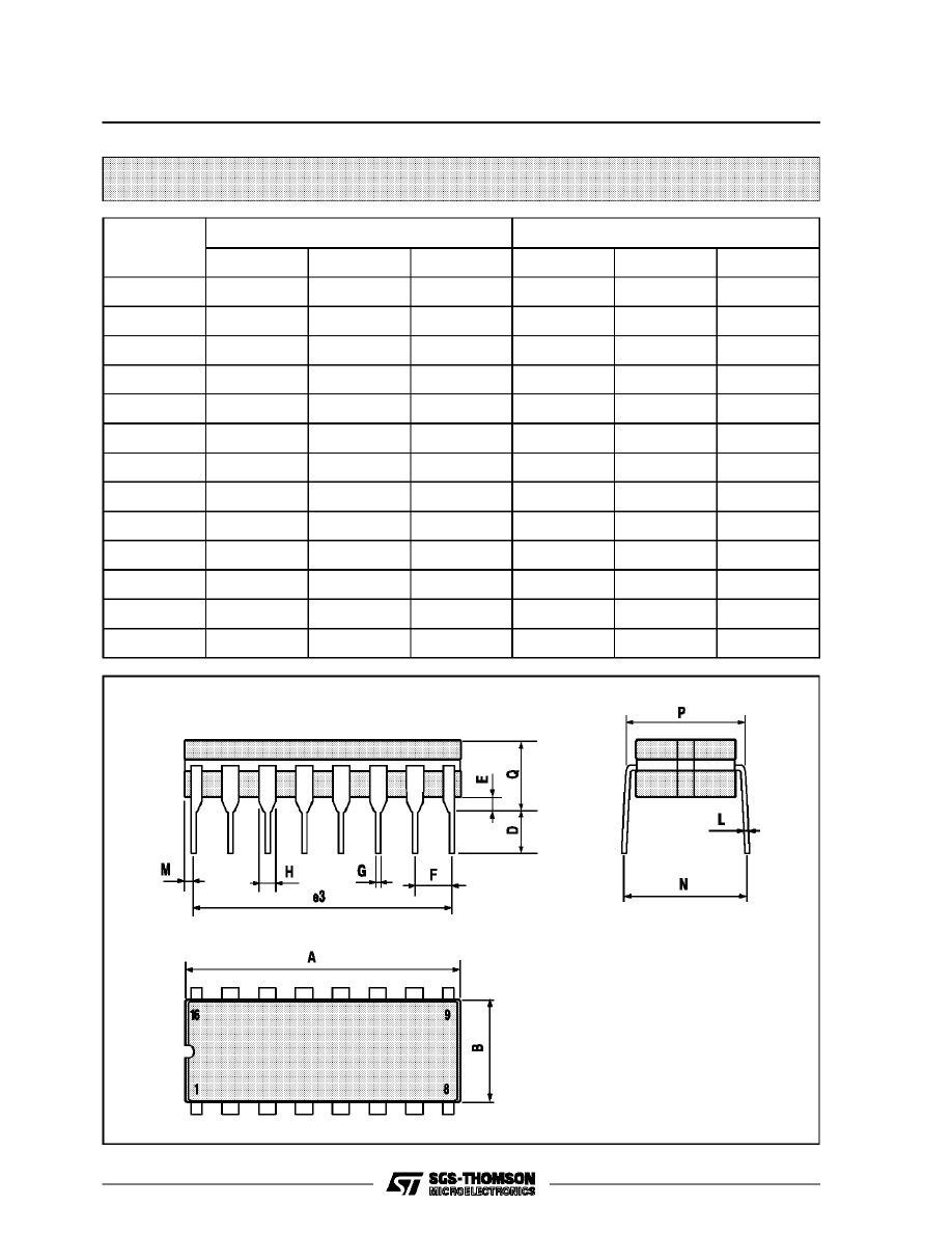
Ceramic DIP16/1 MECHANICAL DATA
DIM.
mm
inch
MIN.
TYP.
MAX.
MIN.
TYP.
MAX.
A
20
0.787
B
7
0.276
D
3.3
0.130
E
0.38
0.015
e3
17.78
0.700
F
2.29
2.79
0.090
0.110
G
0.4
0.55
0.016
0.022
H
1.17
1.52
0.046
0.060
L
0.22
0.31
0.009
0.012
M
0.51
1.27
0.020
0.050
N
10.3
0.406
P
7.8
8.05
0.307
0.317
Q
5.08
0.200
P053D
HCC/HCF4027B
9/12
SO16 (Narrow) MECHANICAL DATA
DIM.
mm
inch
MIN.
TYP.
MAX.
MIN.
TYP.
MAX.
A
1.75
0.068
a1
0.1
0.2
0.004
0.007
a2
1.65
0.064
b
0.35
0.46
0.013
0.018
b1
0.19
0.25
0.007
0.010
C
0.5
0.019
c1
45
°
(typ.)
D
9.8
10
0.385
0.393
E
5.8
6.2
0.228
0.244
e
1.27
0.050
e3
8.89
0.350
F
3.8
4.0
0.149
0.157
G
4.6
5.3
0.181
0.208
L
0.5
1.27
0.019
0.050
M
0.62
0.024
S
8
°
(max.)
P013H
HCC/HCF4027B
10/12
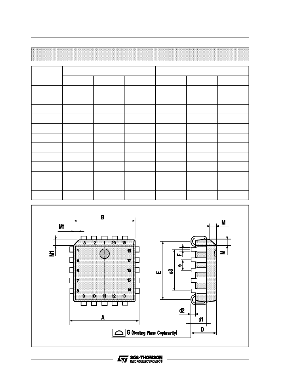
PLCC20 MECHANICAL DATA
DIM.
mm
inch
MIN.
TYP.
MAX.
MIN.
TYP.
MAX.
A
9.78
10.03
0.385
0.395
B
8.89
9.04
0.350
0.356
D
4.2
4.57
0.165
0.180
d1
2.54
0.100
d2
0.56
0.022
E
7.37
8.38
0.290
0.330
e
1.27
0.050
e3
5.08
0.200
F
0.38
0.015
G
0.101
0.004
M
1.27
0.050
M1
1.14
0.045
P027A
HCC/HCF4027B
11/12
Information furnished is believed to be accurate and reliable. However, SGS-THOMSON Microelectronics assumes no responsability for the
consequences of use of such information nor for any infringement of patents or other rights of third parties which may results from its use. No
license is granted by implication or otherwise under any patent or patent rights of SGS-THOMSON Microelectronics. Specifications mentioned
in this publication are subject to change without notice. This publication supersedes and replaces all information previously supplied.
SGS-THOMSON Microelectronics products are not authorized for use as critical components in life support devices or systems without express
written approval of SGS-THOMSON Microelectonics.
1994 SGS-THOMSON Microelectronics - All Rights Reserved
SGS-THOMSON Microelectronics GROUP OF COMPANIES
Australia - Brazil - France - Germany - Hong Kong - Italy - Japan - Korea - Malaysia - Malta - Morocco - The Netherlands -
Singapore - Spain - Sweden - Switzerland - Taiwan - Thailand - United Kingdom - U.S.A
HCC/HCF4027B
12/12
Wyszukiwarka
Podobne podstrony:
4027
4027
4027
4027
4027
4027
4027
4027 (Philips)
4027 a
4027 ac
więcej podobnych podstron