September 1990
Order Number: 231455-005
8086
16-BIT HMOS MICROPROCESSOR
8086/8086-2/8086-1
Y
Direct Addressing Capability 1 MByte
of Memory
Y
Architecture Designed for Powerful
Assembly Language and Efficient High
Level Languages
Y
14 Word, by 16-Bit Register Set with
Symmetrical Operations
Y
24 Operand Addressing Modes
Y
Bit, Byte, Word, and Block Operations
Y
8 and 16-Bit Signed and Unsigned
Arithmetic in Binary or Decimal
Including Multiply and Divide
Y
Range of Clock Rates:
5 MHz for 8086,
8 MHz for 8086-2,
10 MHz for 8086-1
Y
MULTIBUS System Compatible
Interface
Y
Available in EXPRESS
Ð Standard Temperature Range
Ð Extended Temperature Range
Y
Available in 40-Lead Cerdip and Plastic
Package
(See Packaging Spec. Order
Ý
231369)
The Intel 8086 high performance 16-bit CPU is available in three clock rates: 5, 8 and 10 MHz. The CPU is
implemented in N-Channel, depletion load, silicon gate technology (HMOS-III), and packaged in a 40-pin
CERDIP or plastic package. The 8086 operates in both single processor and multiple processor configurations
to achieve high performance levels.
231455 – 1
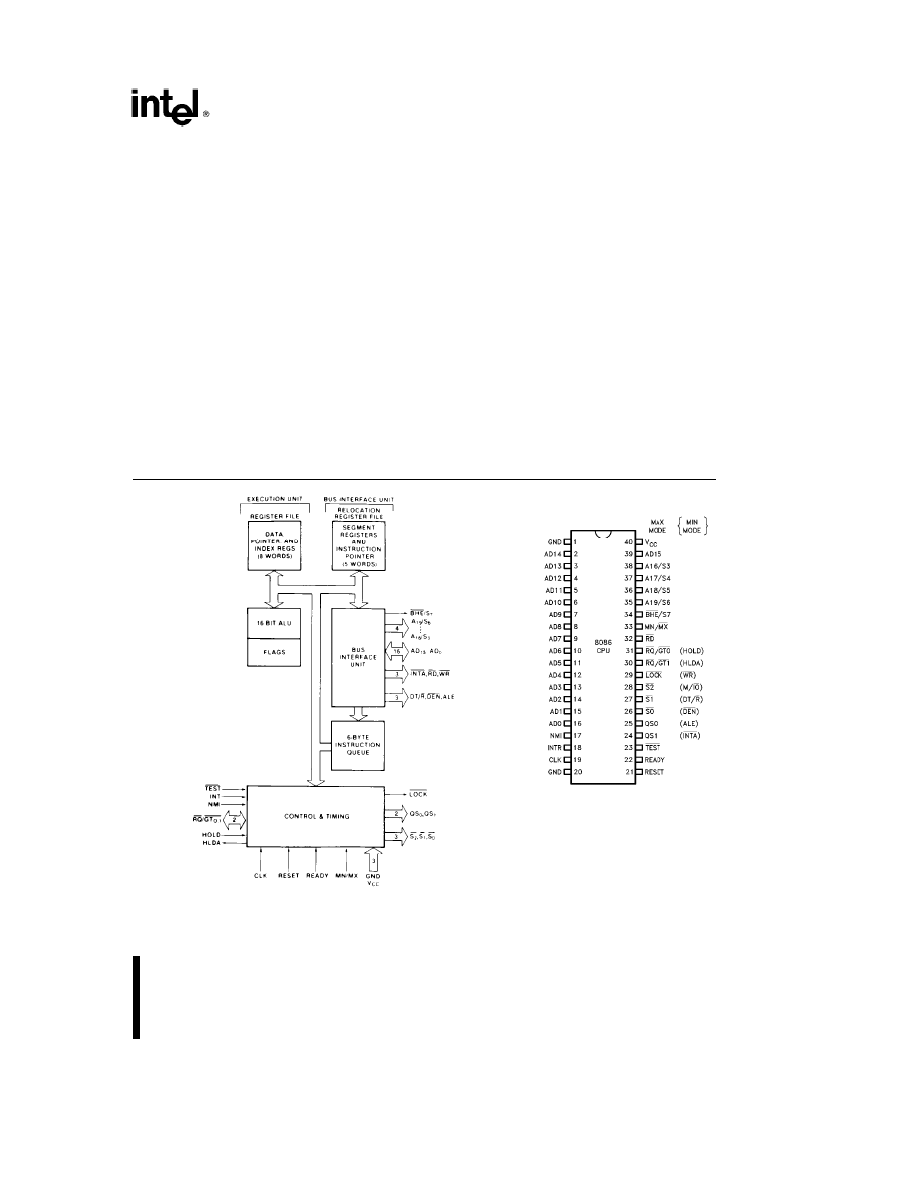
Figure 1. 8086 CPU Block Diagram
231455 – 2
40 Lead
Figure 2. 8086 Pin
Configuration
8086
Table 1. Pin Description
The following pin function descriptions are for 8086 systems in either minimum or maximum mode. The ‘‘Local
Bus’’ in these descriptions is the direct multiplexed bus interface connection to the 8086 (without regard to
additional bus buffers).
Symbol
Pin No.
Type
Name and Function
AD
15
– AD
0
2 – 16, 39
I/O
ADDRESS DATA BUS:
These lines constitute the time multiplexed
memory/IO address (T
1
), and data (T
2
, T
3
, T
W
, T
4
) bus. A
0
is
analogous to BHE for the lower byte of the data bus, pins D
7
– D
0
. It is
LOW during T
1
when a byte is to be transferred on the lower portion
of the bus in memory or I/O operations. Eight-bit oriented devices tied
to the lower half would normally use A
0
to condition chip select
functions. (See BHE.) These lines are active HIGH and float to 3-state
OFF during interrupt acknowledge and local bus ‘‘hold acknowledge’’.
A
19
/S
6
,
35 – 38
O
ADDRESS/STATUS:
During T
1
these are the four most significant
address lines for memory operations. During I/O operations these
A
18
/S
5
,
lines are LOW. During memory and I/O operations, status information
A
17
/S
4
,
is available on these lines during T
2
, T
3
, T
W
, T
4
. The status of the
A
16
/S
3
interrupt enable FLAG bit (S
5
) is updated at the beginning of each
CLK cycle. A
17
/S
4
and A
16
/S
3
are encoded as shown.
This information indicates which relocation register is presently being
used for data accessing.
These lines float to 3-state OFF during local bus ‘‘hold acknowledge.’’
A
17
/S
4
A
16
/S
3
Characteristics
0 (LOW)
0
Alternate Data
0
1
Stack
1 (HIGH)
0
Code or None
1
1
Data
S
6
is 0
(LOW)
BHE/S
7
34
O
BUS HIGH ENABLE/STATUS:
During T
1
the bus high enable signal
(BHE) should be used to enable data onto the most significant half of
the data bus, pins D
15
– D
8
. Eight-bit oriented devices tied to the upper
half of the bus would normally use BHE to condition chip select
functions. BHE is LOW during T
1
for read, write, and interrupt
acknowledge cycles when a byte is to be transferred on the high
portion of the bus. The S
7
status information is available during T
2
,
T
3
, and T
4
. The signal is active LOW, and floats to 3-state OFF in
‘‘hold’’. It is LOW during T
1
for the first interrupt acknowledge cycle.
BHE
A
0
Characteristics
0
0
Whole word
0
1
Upper byte from/to odd address
1
0
Lower byte from/to even address
1
1
None
RD
32
O
READ:
Read strobe indicates that the processor is performing a
memory or I/O read cycle, depending on the state of the S
2
pin. This
signal is used to read devices which reside on the 8086 local bus. RD
is active LOW during T
2
, T
3
and T
W
of any read cycle, and is
guaranteed to remain HIGH in T
2
until the 8086 local bus has floated.
This signal floats to 3-state OFF in ‘‘hold acknowledge’’.
2
8086
Table 1. Pin Description
(Continued)
Symbol
Pin No.
Type
Name and Function
READY
22
I
READY:
is the acknowledgement from the addressed memory or I/O
device that it will complete the data transfer. The READY signal from
memory/IO is synchronized by the 8284A Clock Generator to form
READY. This signal is active HIGH. The 8086 READY input is not
synchronized. Correct operation is not guaranteed if the setup and hold
times are not met.
INTR
18
I
INTERRUPT REQUEST:
is a level triggered input which is sampled
during the last clock cycle of each instruction to determine if the
processor should enter into an interrupt acknowledge operation. A
subroutine is vectored to via an interrupt vector lookup table located in
system memory. It can be internally masked by software resetting the
interrupt enable bit. INTR is internally synchronized. This signal is
active HIGH.
TEST
23
I
TEST:
input is examined by the ‘‘Wait’’ instruction. If the TEST input is
LOW execution continues, otherwise the processor waits in an ‘‘Idle’’
state. This input is synchronized internally during each clock cycle on
the leading edge of CLK.
NMI
17
I
NON-MASKABLE INTERRUPT:
an edge triggered input which causes
a type 2 interrupt. A subroutine is vectored to via an interrupt vector
lookup table located in system memory. NMI is not maskable internally
by software. A transition from LOW to HIGH initiates the interrupt at the
end of the current instruction. This input is internally synchronized.
RESET
21
I
RESET:
causes the processor to immediately terminate its present
activity. The signal must be active HIGH for at least four clock cycles. It
restarts execution, as described in the Instruction Set description, when
RESET returns LOW. RESET is internally synchronized.
CLK
19
I
CLOCK:
provides the basic timing for the processor and bus controller.
It is asymmetric with a 33% duty cycle to provide optimized internal
timing.
V
CC
40
V
CC
: a
5V power supply pin.
GND
1, 20
GROUND
MN/MX
33
I
MINIMUM/MAXIMUM:
indicates what mode the processor is to
operate in. The two modes are discussed in the following sections.
The following pin function descriptions are for the 8086/8288 system in maximum mode (i.e., MN/MX
e
V
SS
).
Only the pin functions which are unique to maximum mode are described; all other pin functions are as
described above.
S
2
, S
1
, S
0
26 – 28
O
STATUS:
active during T
4
, T
1
, and T
2
and is returned to the passive state
(1, 1, 1) during T
3
or during T
W
when READY is HIGH. This status is used
by the 8288 Bus Controller to generate all memory and I/O access control
signals. Any change by S
2
, S
1
, or S
0
during T
4
is used to indicate the
beginning of a bus cycle, and the return to the passive state in T
3
or T
W
is
used to indicate the end of a bus cycle.
3
8086
Table 1. Pin Description
(Continued)
Symbol
Pin No.
Type
Name and Function
S
2
, S
1
, S
0
26 – 28
O
These signals float to 3-state OFF in ‘‘hold acknowledge’’. These status
lines are encoded as shown.
(Continued)
S
2
S
1
S
0
Characteristics
0 (LOW)
0
0
Interrupt Acknowledge
0
0
1
Read I/O Port
0
1
0
Write I/O Port
0
1
1
Halt
1 (HIGH)
0
0
Code Access
1
0
1
Read Memory
1
1
0
Write Memory
1
1
1
Passive
RQ/GT
0
,
30, 31
I/O
REQUEST/GRANT:
pins are used by other local bus masters to force
the processor to release the local bus at the end of the processor’s
RQ/GT
1
current bus cycle. Each pin is bidirectional with RQ/GT
0
having higher
priority than RQ/GT
1
. RQ/GT pins have internal pull-up resistors and
may be left unconnected. The request/grant sequence is as follows
(see Page 2-24):
1. A pulse of 1 CLK wide from another local bus master indicates a local
bus request (‘‘hold’’) to the 8086 (pulse 1).
2. During a T
4
or T
1
clock cycle, a pulse 1 CLK wide from the 8086 to
the requesting master (pulse 2), indicates that the 8086 has allowed the
local bus to float and that it will enter the ‘‘hold acknowledge’’ state at
the next CLK. The CPU’s bus interface unit is disconnected logically
from the local bus during ‘‘hold acknowledge’’.
3. A pulse 1 CLK wide from the requesting master indicates to the 8086
(pulse 3) that the ‘‘hold’’ request is about to end and that the 8086 can
reclaim the local bus at the next CLK.
Each master-master exchange of the local bus is a sequence of 3
pulses. There must be one dead CLK cycle after each bus exchange.
Pulses are active LOW.
If the request is made while the CPU is performing a memory cycle, it
will release the local bus during T
4
of the cycle when all the following
conditions are met:
1. Request occurs on or before T
2
.
2. Current cycle is not the low byte of a word (on an odd address).
3. Current cycle is not the first acknowledge of an interrupt acknowledge
sequence.
4. A locked instruction is not currently executing.
If the local bus is idle when the request is made the two possible events
will follow:
1. Local bus will be released during the next clock.
2. A memory cycle will start within 3 clocks. Now the four rules for a
currently active memory cycle apply with condition number 1 already
satisfied.
LOCK
29
O
LOCK:
output indicates that other system bus masters are not to gain
control of the system bus while LOCK is active LOW. The LOCK signal
is activated by the ‘‘LOCK’’ prefix instruction and remains active until the
completion of the next instruction. This signal is active LOW, and floats
to 3-state OFF in ‘‘hold acknowledge’’.
4
8086
Table 1. Pin Description
(Continued)
Symbol
Pin No.
Type
Name and Function
QS
1
, QS
0
24, 25
O
QUEUE STATUS:
The queue status is valid during the CLK cycle after
which the queue operation is performed.
QS
1
and QS
0
provide status to allow external tracking of the internal
8086 instruction queue.
QS
1
QS
0
Characteristics
0 (LOW)
0
No Operation
0
1
First Byte of Op Code from Queue
1 (HIGH)
0
Empty the Queue
1
1
Subsequent Byte from Queue
The following pin function descriptions are for the 8086 in minimum mode (i.e., MN/MX
e
V
CC
). Only the pin
functions which are unique to minimum mode are described; all other pin functions are as described above.
M/IO
28
O
STATUS LINE:
logically equivalent to S
2
in the maximum mode. It is used to
distinguish a memory access from an I/O access. M/IO becomes valid in
the T
4
preceding a bus cycle and remains valid until the final T
4
of the cycle
(M e HIGH, IO e LOW). M/IO floats to 3-state OFF in local bus ‘‘hold
acknowledge’’.
WR
29
O
WRITE:
indicates that the processor is performing a write memory or write
I/O cycle, depending on the state of the M/IO signal. WR is active for T
2
, T
3
and T
W
of any write cycle. It is active LOW, and floats to 3-state OFF in
local bus ‘‘hold acknowledge’’.
INTA
24
O
INTA:
is used as a read strobe for interrupt acknowledge cycles. It is active
LOW during T
2
, T
3
and T
W
of each interrupt acknowledge cycle.
ALE
25
O
ADDRESS LATCH ENABLE:
provided by the processor to latch the
address into the 8282/8283 address latch. It is a HIGH pulse active during
T
1
of any bus cycle. Note that ALE is never floated.
DT/R
27
O
DATA TRANSMIT/RECEIVE:
needed in minimum system that desires to
use an 8286/8287 data bus transceiver. It is used to control the direction of
data flow through the transceiver. Logically DT/R is equivalent to S
1
in the
maximum mode, and its timing is the same as for M/IO. (T e HIGH, R e
LOW.) This signal floats to 3-state OFF in local bus ‘‘hold acknowledge’’.
DEN
26
O
DATA ENABLE:
provided as an output enable for the 8286/8287 in a
minimum system which uses the transceiver. DEN is active LOW during
each memory and I/O access and for INTA cycles. For a read or INTA cycle
it is active from the middle of T
2
until the middle of T
4
, while for a write cycle
it is active from the beginning of T
2
until the middle of T
4
. DEN floats to 3-
state OFF in local bus ‘‘hold acknowledge’’.
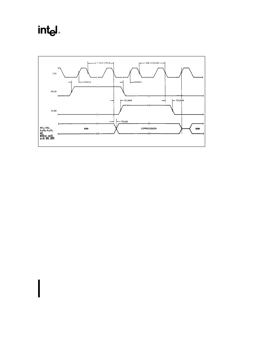
HOLD,
31, 30
I/O
HOLD:
indicates that another master is requesting a local bus ‘‘hold.’’ To be
acknowledged, HOLD must be active HIGH. The processor receiving the
HLDA
‘‘hold’’ request will issue HLDA (HIGH) as an acknowledgement in the
middle of a T
4
or T
i
clock cycle. Simultaneous with the issuance of HLDA
the processor will float the local bus and control lines. After HOLD is
detected as being LOW, the processor will LOWer the HLDA, and when the
processor needs to run another cycle, it will again drive the local bus and
control lines. Hold acknowledge (HLDA) and HOLD have internal pull-up
resistors.
The same rules as for RQ/GT apply regarding when the local bus will be
released.
HOLD is not an asynchronous input. External synchronization should be
provided if the system cannot otherwise guarantee the setup time.
5
8086
FUNCTIONAL DESCRIPTION
General Operation
The internal functions of the 8086 processor are
partitioned logically into two processing units. The
first is the Bus Interface Unit (BIU) and the second is
the Execution Unit (EU) as shown in the block dia-
gram of Figure 1.
These units can interact directly but for the most
part perform as separate asynchronous operational
processors. The bus interface unit provides the func-
tions related to instruction fetching and queuing, op-
erand fetch and store, and address relocation. This
unit also provides the basic bus control. The overlap
of instruction pre-fetching provided by this unit
serves to increase processor performance through
improved bus bandwidth utilization. Up to 6 bytes of
the instruction stream can be queued while waiting
for decoding and execution.
The instruction stream queuing mechanism allows
the BIU to keep the memory utilized very efficiently.
Whenever there is space for at least 2 bytes in the
queue, the BIU will attempt a word fetch memory
cycle. This greatly reduces ‘‘dead time’’ on the
memory bus. The queue acts as a First-In-First-Out
(FIFO) buffer, from which the EU extracts instruction
bytes as required. If the queue is empty (following a
branch instruction, for example), the first byte into
the queue immediately becomes available to the EU.
The execution unit receives pre-fetched instructions
from the BIU queue and provides un-relocated oper-
and addresses to the BIU. Memory operands are
passed through the BIU for processing by the EU,
which passes results to the BIU for storage. See the
Instruction Set description for further register set
and architectural descriptions.
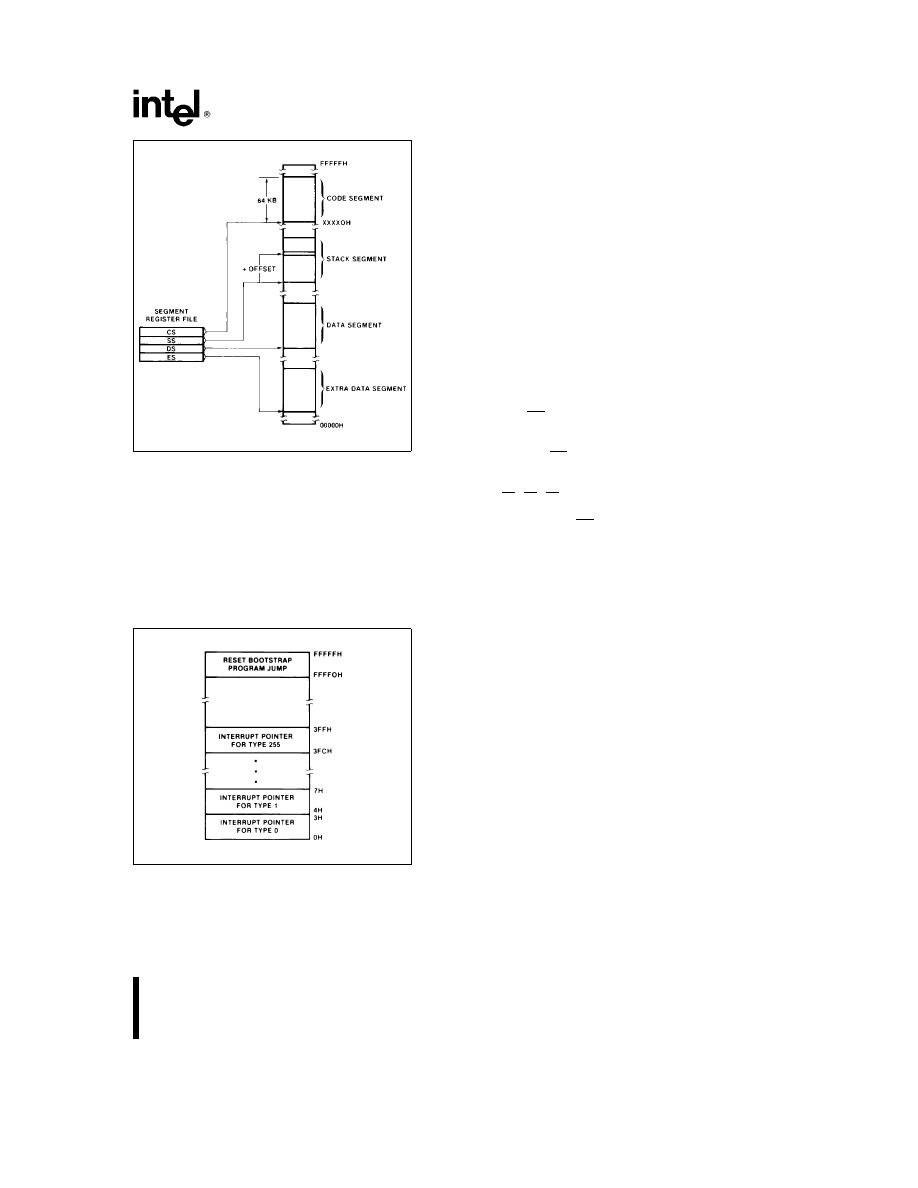
MEMORY ORGANIZATION
The processor provides a 20-bit address to memory
which locates the byte being referenced. The memo-
ry is organized as a linear array of up to 1 million
bytes, addressed as 00000(H) to FFFFF(H). The
memory is logically divided into code, data, extra
data, and stack segments of up to 64K bytes each,
with each segment falling on 16-byte boundaries.
(See Figure 3a.)
All memory references are made relative to base ad-
dresses contained in high speed segment registers.
The segment types were chosen based on the ad-
dressing needs of programs. The segment register
to be selected is automatically chosen according to
the rules of the following table. All information in one
segment type share the same logical attributes (e.g.
code or data). By structuring memory into relocat-
able areas of similar characteristics and by automati-
cally selecting segment registers, programs are
shorter, faster, and more structured.
Word (16-bit) operands can be located on even or
odd address boundaries and are thus not con-
strained to even boundaries as is the case in many
16-bit computers. For address and data operands,
the least significant byte of the word is stored in the
lower valued address location and the most signifi-
cant byte in the next higher address location. The
BIU automatically performs the proper number of
memory accesses, one if the word operand is on an
even byte boundary and two if it is on an odd byte
boundary. Except for the performance penalty, this
double access is transparent to the software. This
performance penalty does not occur for instruction
fetches, only word operands.
Physically, the memory is organized as a high bank
(D
15
– D
8
) and a low bank (D
7
– D
0
) of 512K 8-bit
bytes addressed in parallel by the processor’s ad-
dress lines A
19
– A
1
. Byte data with even addresses
is transferred on the D
7
– D
0
bus lines while odd ad-
dressed byte data (A
0
HIGH) is transferred on the
D
15
– D
8
bus lines. The processor provides two en-
able signals, BHE and A
0
, to selectively allow read-
ing from or writing into either an odd byte location,
even byte location, or both. The instruction stream is
fetched from memory as words and is addressed
internally by the processor to the byte level as nec-
essary.
Memory
Segment Register
Segment
Reference Need
Used
Selection Rule
Instructions
CODE (CS)
Automatic with all instruction prefetch.
Stack
STACK (SS)
All stack pushes and pops. Memory references relative to BP
base register except data references.
Local Data
DATA (DS)
Data references when: relative to stack, destination of string
operation, or explicitly overridden.
External (Global) Data
EXTRA (ES)
Destination of string operations: explicitly selected using a
segment override.
6
8086
231455 – 3
Figure 3a. Memory Organization
In referencing word data the BIU requires one or two
memory cycles depending on whether or not the
starting byte of the word is on an even or odd ad-
dress, respectively. Consequently, in referencing
word operands performance can be optimized by lo-
cating data on even address boundaries. This is an
especially useful technique for using the stack, since
odd address references to the stack may adversely
affect the context switching time for interrupt pro-
cessing or task multiplexing.
231455 – 4
Figure 3b. Reserved Memory Locations
Certain locations in memory are reserved for specific
CPU operations (see Figure 3b). Locations from
address FFFF0H through FFFFFH are reserved for
operations including a jump to the initial program
loading routine. Following RESET, the CPU will al-
ways begin execution at location FFFF0H where the
jump must be. Locations 00000H through 003FFH
are reserved for interrupt operations. Each of the
256 possible interrupt types has its service routine
pointed to by a 4-byte pointer element consisting of
a 16-bit segment address and a 16-bit offset ad-
dress. The pointer elements are assumed to have
been stored at the respective places in reserved
memory prior to occurrence of interrupts.
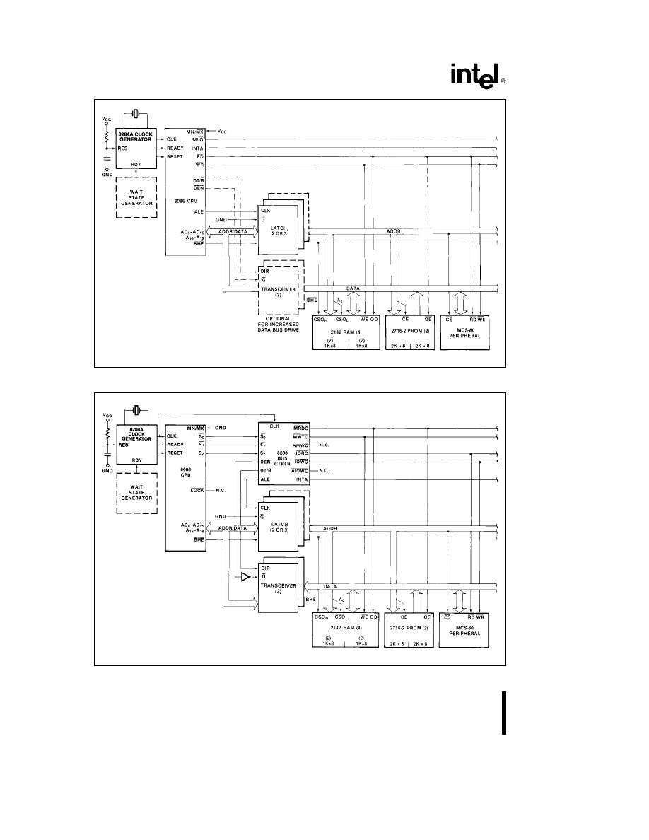
MINIMUM AND MAXIMUM MODES
The requirements for supporting minimum and maxi-
mum 8086 systems are sufficiently different that
they cannot be done efficiently with 40 uniquely de-
fined pins. Consequently, the 8086 is equipped with
a strap pin (MN/MX) which defines the system con-
figuration. The definition of a certain subset of the
pins changes dependent on the condition of the
strap pin. When MN/MX pin is strapped to GND, the
8086 treats pins 24 through 31 in maximum mode.
An 8288 bus controller interprets status information
coded into S
0
, S
2
, S
2
to generate bus timing and
control signals compatible with the MULTIBUS ar-
chitecture. When the MN/MX pin is strapped to V
CC
,
the 8086 generates bus control signals itself on pins
24 through 31, as shown in parentheses in Figure 2.
Examples of minimum mode and maximum mode
systems are shown in Figure 4.
BUS OPERATION
The 8086 has a combined address and data bus
commonly referred to as a time multiplexed bus.
This technique provides the most efficient use of
pins on the processor while permitting the use of a
standard 40-lead package. This ‘‘local bus’’ can be
buffered directly and used throughout the system
with address latching provided on memory and I/O
modules. In addition, the bus can also be demulti-
plexed at the processor with a single set of address
latches if a standard non-multiplexed bus is desired
for the system.
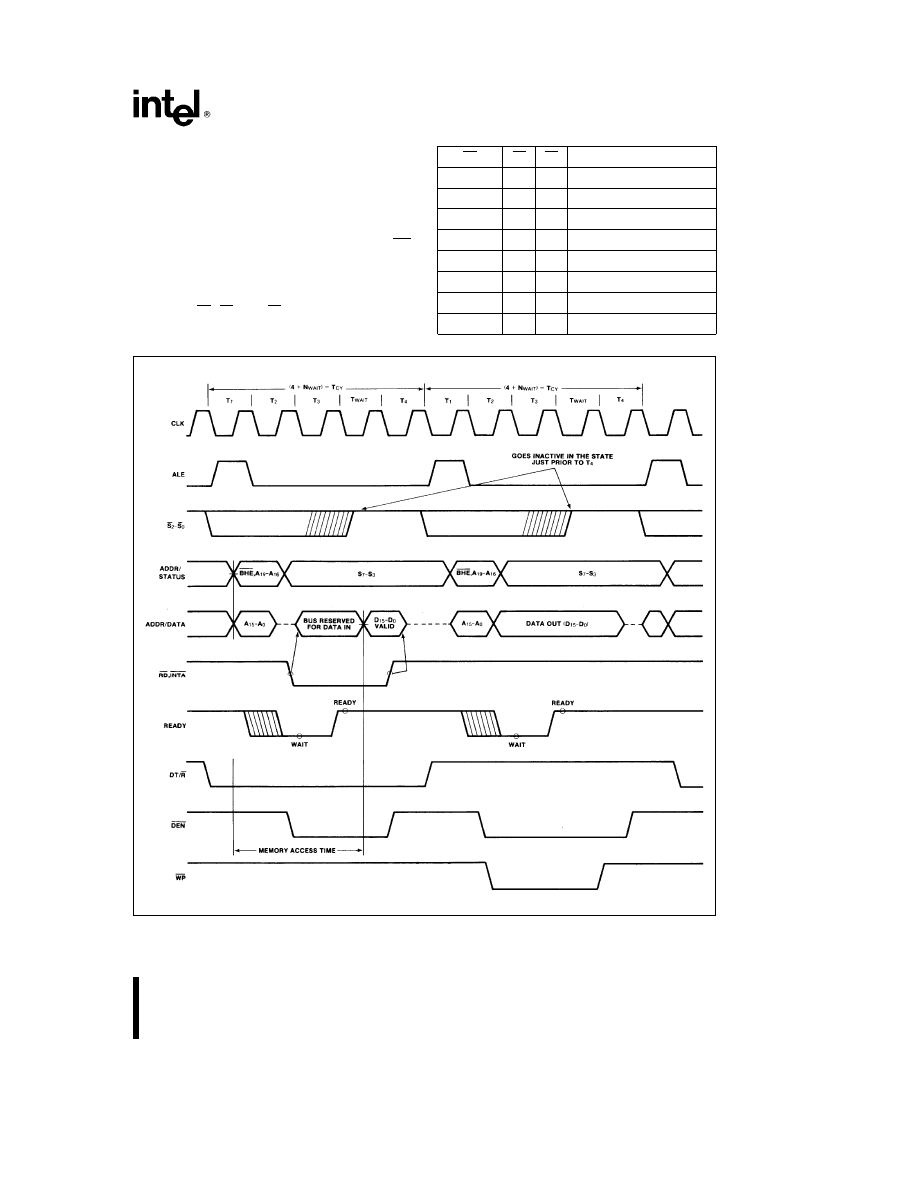
Each processor bus cycle consists of at least four
CLK cycles. These are referred to as T
1
, T
2
, T
3
and
T
4
(see Figure 5). The address is emitted from the
processor during T
1
and data transfer occurs on the
bus during T
3
and T
4
. T
2
is used primarily for chang-
ing the direction of the bus during read operations. In
the event that a ‘‘NOT READY’’ indication is given
by the addressed device, ‘‘Wait’’ states (T
W
) are in-
serted between T
3
and T
4
. Each inserted ‘‘Wait’’
state is of the same duration as a CLK cycle. Periods
7
8086
231455 – 5
Figure 4a. Minimum Mode 8086 Typical Configuration
231455 – 6
Figure 4b. Maximum Mode 8086 Typical Configuration
8
8086
can occur between 8086 bus cycles. These are re-
ferred to as ‘‘Idle’’ states (T
i
) or inactive CLK cycles.
The processor uses these cycles for internal house-
keeping.
During T
1
of any bus cycle the ALE (Address Latch
Enable) signal is emitted (by either the processor or
the 8288 bus controller, depending on the MN/MX
strap). At the trailing edge of this pulse, a valid ad-
dress and certain status information for the cycle
may be latched.
Status bits S
0
, S
1
, and S
2
are used, in maximum
mode, by the bus controller to identify the type of
bus transaction according to the following table:
S
2
S
1
S
0
Characteristics
0 (LOW)
0
0
Interrupt Acknowledge
0
0
1
Read I/O
0
1
0
Write I/O
0
1
1
Halt
1 (HIGH)
0
0
Instruction Fetch
1
0
1
Read Data from Memory
1
1
0
Write Data to Memory
1
1
1
Passive (no bus cycle)
231455 – 8
Figure 5. Basic System Timing
9
8086
Status bits S
3
through S
7
are multiplexed with high-
order address bits and the BHE signal, and are
therefore valid during T
2
through T
4
. S
3
and S
4
indi-
cate which segment register (see Instruction Set de-
scription) was used for this bus cycle in forming the
address, according to the following table:
S
4
S
3
Characteristics
0 (LOW)
0
Alternate Data (extra segment)
0
1
Stack
1 (HIGH)
0
Code or None
1
1
Data
S
5
is a reflection of the PSW interrupt enable bit.
S
6
e
0 and S
7
is a spare status bit.
I/O ADDRESSING
In the 8086, I/O operations can address up to a
maximum of 64K I/O byte registers or 32K I/O word
registers. The I/O address appears in the same for-
mat as the memory address on bus lines A
15
– A
0
.
The address lines A
19
– A
16
are zero in I/O opera-
tions. The variable I/O instructions which use regis-
ter DX as a pointer have full address capability while
the direct I/O instructions directly address one or
two of the 256 I/O byte locations in page 0 of the
I/O address space.
I/O ports are addressed in the same manner as
memory locations. Even addressed bytes are trans-
ferred on the D
7
– D
0
bus lines and odd addressed
bytes on D
15
– D
8
. Care must be taken to assure that
each register within an 8-bit peripheral located on
the lower portion of the bus be addressed as even.
External Interface
PROCESSOR RESET AND INITIALIZATION
Processor initialization or start up is accomplished
with activation (HIGH) of the RESET pin. The 8086
RESET is required to be HIGH for greater than 4
CLK cycles. The 8086 will terminate operations on
the high-going edge of RESET and will remain dor-
mant as long as RESET is HIGH. The low-going
transition of RESET triggers an internal reset se-
quence for approximately 10 CLK cycles. After this
interval the 8086 operates normally beginning with
the instruction in absolute location FFFF0H (see Fig-
ure 3b). The details of this operation are specified in
the Instruction Set description of the MCS-86 Family
User’s Manual. The RESET input is internally syn-
chronized to the processor clock. At initialization the
HIGH-to-LOW transition of RESET must occur no
sooner than 50 ms after power-up, to allow complete
initialization of the 8086.
NMI asserted prior to the 2nd clock after the end of
RESET will not be honored. If NMI is asserted after
that point and during the internal reset sequence,
the processor may execute one instruction before
responding to the interrupt. A hold request active
immediately after RESET will be honored before the
first instruction fetch.
All 3-state outputs float to 3-state OFF during
RESET. Status is active in the idle state for the first
clock after RESET becomes active and then floats
to 3-state OFF. ALE and HLDA are driven low.
INTERRUPT OPERATIONS
Interrupt operations fall into two classes; software or
hardware initiated. The software initiated interrupts
and software aspects of hardware interrupts are
specified in the Instruction Set description. Hard-
ware interrupts can be classified as non-maskable or
maskable.
Interrupts result in a transfer of control to a new pro-
gram location. A 256-element table containing ad-
dress pointers to the interrupt service program loca-
tions resides in absolute locations 0 through 3FFH
(see Figure 3b), which are reserved for this purpose.
Each element in the table is 4 bytes in size and
corresponds to an interrupt ‘‘type’’. An interrupting
device supplies an 8-bit type number, during the in-
terrupt acknowledge sequence, which is used to
‘‘vector’’ through the appropriate element to the new
interrupt service program location.
NON-MASKABLE INTERRUPT (NMI)
The processor provides a single non-maskable inter-
rupt pin (NMI) which has higher priority than the
maskable interrupt request pin (INTR). A typical use
would be to activate a power failure routine. The
NMI is edge-triggered on a LOW-to-HIGH transition.
The activation of this pin causes a type 2 interrupt.
(See Instruction Set description.)
NMI is required to have a duration in the HIGH state
of greater than two CLK cycles, but is not required to
be synchronized to the clock. Any high-going tran-
sition of NMI is latched on-chip and will be serviced
at the end of the current instruction or between
whole moves of a block-type instruction. Worst case
response to NMI would be for multiply, divide, and
variable shift instructions. There is no specification
on the occurrence of the low-going edge; it may oc-
cur before, during, or after the servicing of NMI. An-
other high-going edge triggers another response if it
occurs after the start of the NMI procedure. The sig-
nal must be free of logical spikes in general and be
free of bounces on the low-going edge to avoid trig-
gering extraneous responses.
10
8086
MASKABLE INTERRUPT (INTR)
The 8086 provides a single interrupt request input
(INTR) which can be masked internally by software
with the resetting of the interrupt enable FLAG
status bit. The interrupt request signal is level trig-
gered. It is internally synchronized during each clock
cycle on the high-going edge of CLK. To be re-
sponded to, INTR must be present (HIGH) during
the clock period preceding the end of the current
instruction or the end of a whole move for a block-
type instruction. During the interrupt response se-
quence further interrupts are disabled. The enable
bit is reset as part of the response to any interrupt
(INTR, NMI, software interrupt or single-step), al-
though the FLAGS register which is automatically
pushed onto the stack reflects the state of the proc-
essor prior to the interrupt. Until the old FLAGS reg-
ister is restored the enable bit will be zero unless
specifically set by an instruction.
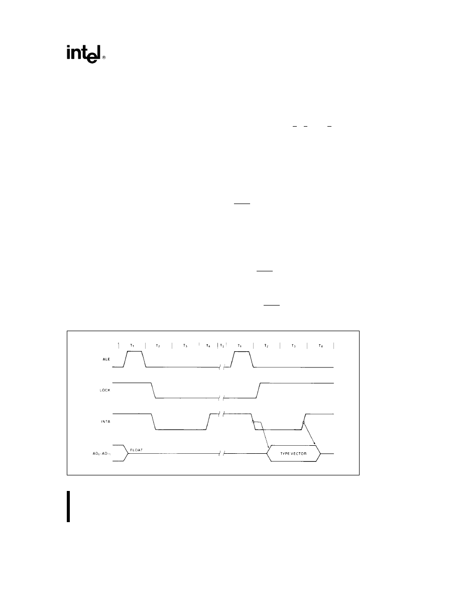
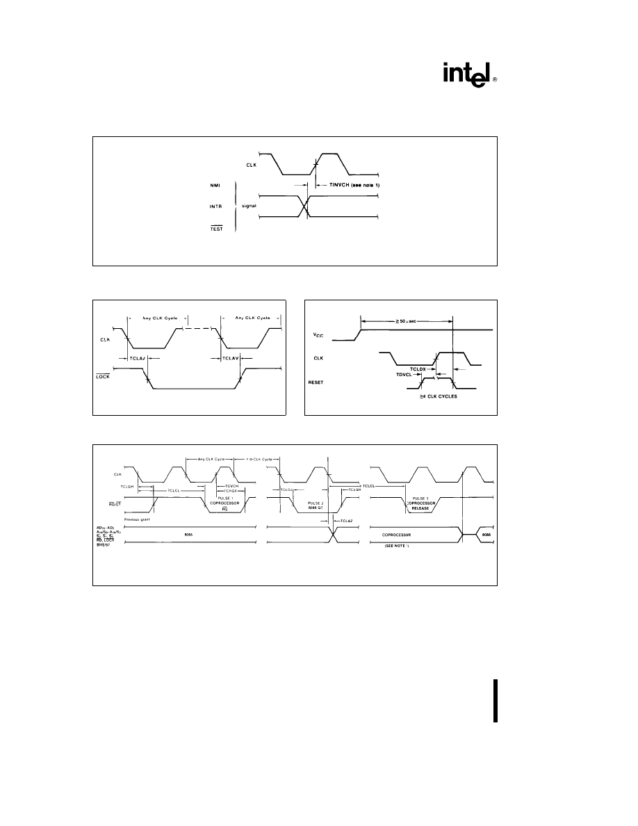
During the response sequence (Figure 6) the proc-
essor executes two successive (back-to-back) inter-
rupt acknowledge cycles. The 8086 emits the LOCK
signal from T
2
of the first bus cycle until T
2
of the
second. A local bus ‘‘hold’’ request will not be hon-
ored until the end of the second bus cycle. In the
second bus cycle a byte is fetched from the external
interrupt system (e.g., 8259A PIC) which identifies
the source (type) of the interrupt. This byte is multi-
plied by four and used as a pointer into the interrupt
vector lookup table. An INTR signal left HIGH will be
continually responded to within the limitations of the
enable bit and sample period. The INTERRUPT RE-
TURN instruction includes a FLAGS pop which re-
turns the status of the original interrupt enable bit
when it restores the FLAGS.
HALT
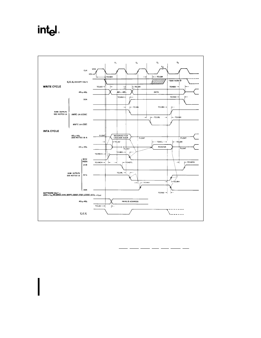
When a software ‘‘HALT’’ instruction is executed the
processor indicates that it is entering the ‘‘HALT’’
state in one of two ways depending upon which
mode is strapped. In minimum mode, the processor
issues one ALE with no qualifying bus control sig-
nals. In maximum mode, the processor issues ap-
propriate HALT status on S
2
, S
1
, and S
0
; and the
8288 bus controller issues one ALE. The 8086 will
not leave the ‘‘HALT’’ state when a local bus ‘‘hold’’
is entered while in ‘‘HALT’’. In this case, the proces-
sor reissues the HALT indicator. An interrupt request
or RESET will force the 8086 out of the ‘‘HALT’’
state.
READ/MODIFY/WRITE (SEMAPHORE)
OPERATIONS VIA LOCK
The LOCK status information is provided by the
processor when directly consecutive bus cycles are
required
during
the
execution
of
an
instruc-
tion. This provides the processor with the capability
of performing read/modify/write operations on
memory (via the Exchange Register With Memory
instruction, for example) without the possibility of an-
other system bus master receiving intervening mem-
ory cycles. This is useful in multi-processor system
configurations to accomplish ‘‘test and set lock’’ op-
erations. The LOCK signal is activated (forced LOW)
in the clock cycle following the one in which the soft-
ware ‘‘LOCK’’ prefix instruction is decoded by the
EU. It is deactivated at the end of the last bus cycle
of the instruction following the ‘‘LOCK’’ prefix in-
struction. While LOCK is active a request on a RQ/
GT pin will be recorded and then honored at the end
of the LOCK.
231455 – 9
Figure 6. Interrupt Acknowledge Sequence
11
8086
EXTERNAL SYNCHRONIZATION VIA TEST
As an alternative to the interrupts and general I/O
capabilities, the 8086 provides a single software-
testable input known as the TEST signal. At any time
the program may execute a WAIT instruction. If at
that time the TEST signal is inactive (HIGH), pro-
gram execution becomes suspended while the proc-
essor waits for TEST to become active. It must
remain active for at least 5 CLK cycles. The WAIT
instruction is re-executed repeatedly until that time.
This activity does not consume bus cycles. The
processor remains in an idle state while waiting. All
8086 drivers go to 3-state OFF if bus ‘‘Hold’’ is en-
tered. If interrupts are enabled, they may occur while
the processor is waiting. When this occurs the proc-
essor fetches the WAIT instruction one extra time,
processes the interrupt, and then re-fetches and re-
executes the WAIT instruction upon returning from
the interrupt.
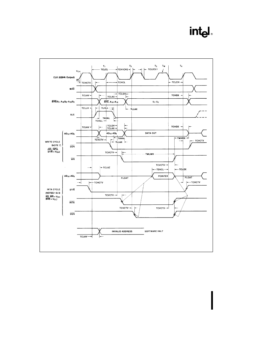
Basic System Timing
Typical system configurations for the processor op-
erating in minimum mode and in maximum mode are
shown in Figures 4a and 4b, respectively. In mini-
mum mode, the MN/MX pin is strapped to V
CC
and
the processor emits bus control signals in a manner
similar to the 8085. In maximum mode, the MN/MX
pin is strapped to V
SS
and the processor emits cod-
ed status information which the 8288 bus controller
uses to generate MULTIBUS compatible bus control
signals. Figure 5 illustrates the signal timing relation-
ships.
231455 – 10
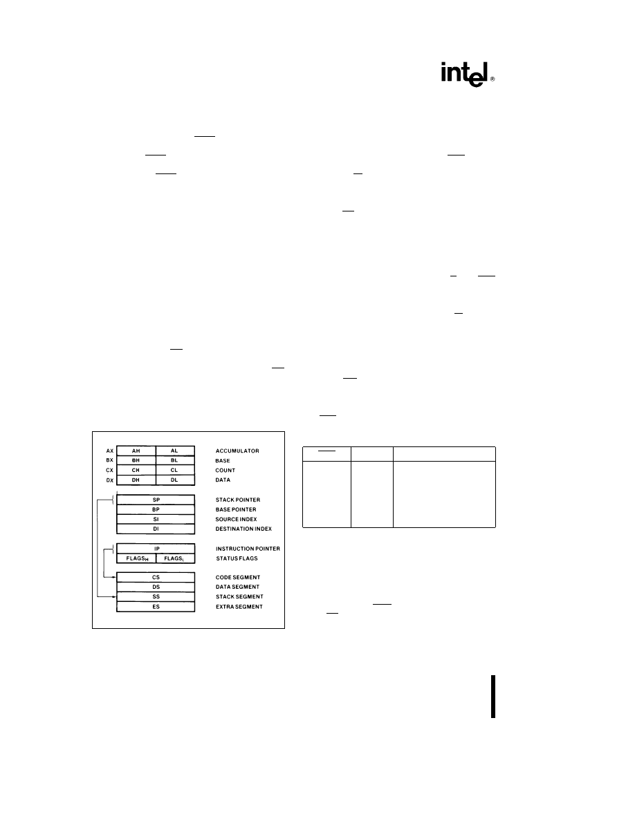
Figure 7. 8086 Register Model
SYSTEM TIMINGÐMINIMUM SYSTEM
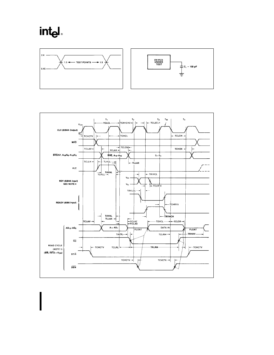
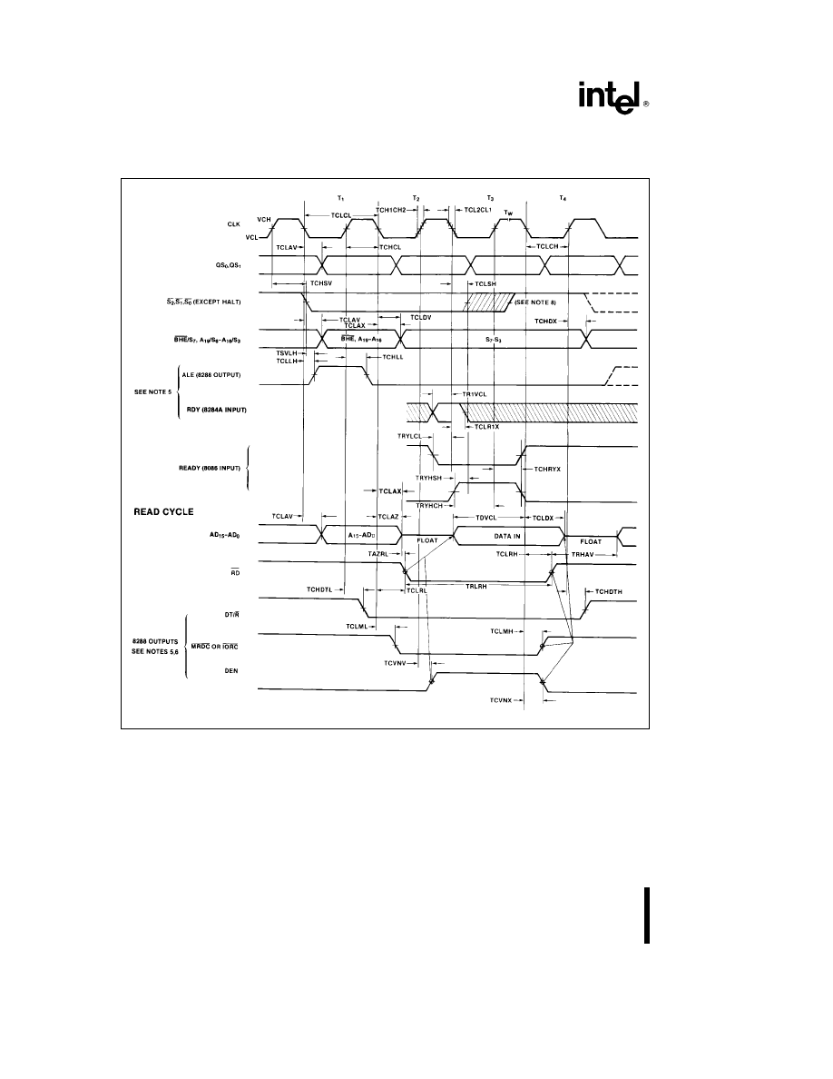
The read cycle begins in T
1
with the assertion of the
Address Latch Enable (ALE) signal. The trailing (low-
going) edge of this signal is used to latch the ad-
dress information, which is valid on the local bus at
this time, into the address latch. The BHE and A
0
signals address the low, high, or both bytes. From T
1
to T
4
the M/IO signal indicates a memory or I/O
operation. At T
2
the address is removed from the
local bus and the bus goes to a high impedance
state. The read control signal is also asserted at T
2
.
The read (RD) signal causes the addressed device
to enable its data bus drivers to the local bus. Some
time later valid data will be available on the bus and
the addressed device will drive the READY line
HIGH. When the processor returns the read signal to
a HIGH level, the addressed device will again 3-
state its bus drivers. If a transceiver is required to
buffer the 8086 local bus, signals DT/R and DEN
are provided by the 8086.
A write cycle also begins with the assertion of ALE
and the emission of the address. The M/IO signal is
again asserted to indicate a memory or I/O write
operation. In the T
2
immediately following the ad-
dress emission the processor emits the data to be
written into the addressed location. This data re-
mains valid until the middle of T
4
. During T
2
, T
3
, and
T
W
the processor asserts the write control signal.
The write (WR) signal becomes active at the begin-
ning of T
2
as opposed to the read which is delayed
somewhat into T
2
to provide time for the bus to float.
The BHE and A
0
signals are used to select the prop-
er byte(s) of the memory/IO word to be read or writ-
ten according to the following table:
BHE
A0
Characteristics
0
0
Whole word
0
1
Upper byte from/to
odd address
1
0
Lower byte from/to
even address
1
1
None
I/O ports are addressed in the same manner as
memory location. Even addressed bytes are trans-
ferred on the D
7
– D
0
bus lines and odd addressed
bytes on D
15
– D
8
.
The basic difference between the interrupt acknowl-
edge cycle and a read cycle is that the interrupt ac-
knowledge signal (INTA) is asserted in place of the
read (RD) signal and the address bus is floated.
(See Figure 6.) In the second of two successive
INTA cycles, a byte of information is read from bus
12

8086
lines D
7
– D
0
as supplied by the inerrupt system logic
(i.e., 8259A Priority Interrupt Controller). This byte
identifies the source (type) of the interrupt. It is multi-
plied by four and used as a pointer into an interrupt
vector lookup table, as described earlier.
BUS TIMINGÐMEDIUM SIZE SYSTEMS
For medium size systems the MN/MX pin is con-
nected to V
SS
and the 8288 Bus Controller is added
to the system as well as a latch for latching the sys-
tem address, and a transceiver to allow for bus load-
ing greater than the 8086 is capable of handling.
Signals ALE, DEN, and DT/R are generated by the
8288 instead of the processor in this configuration
although their timing remains relatively the same.
The 8086 status outputs (S
2
, S
1
, and S
0
) provide
type-of-cycle information and become 8288 inputs.
This bus cycle information specifies read (code,
data,
or
I/O),
write
(data
or
I/O),
interrupt
acknowledge, or software halt. The 8288 thus issues
control signals specifying memory read or write, I/O
read or write, or interrupt acknowledge. The 8288
provides two types of write strobes, normal and ad-
vanced, to be applied as required. The normal write
strobes have data valid at the leading edge of write.
The advanced write strobes have the same timing
as read strobes, and hence data isn’t valid at the
leading edge of write. The transceiver receives the
usual DIR and G inputs from the 8288’s DT/R and
DEN.
The pointer into the interrupt vector table, which is
passed during the second INTA cycle, can derive
from an 8259A located on either the local bus or the
system bus. If the master 8259A Priority Interrupt
Controller is positioned on the local bus, a TTL gate
is required to disable the transceiver when reading
from the master 8259A during the interrupt acknowl-
edge sequence and software ‘‘poll’’.
13
8086
ABSOLUTE MAXIMUM RATINGS
*
Ambient Temperature Under Bias ÀÀÀÀÀÀ0
§
C to 70
§
C
Storage Temperature ÀÀÀÀÀÀÀÀÀÀb65
§
C to a150
§
C
Voltage on Any Pin with
Respect to GroundÀÀÀÀÀÀÀÀÀÀÀÀÀÀb1.0V to a7V
Power DissipationÀÀÀÀÀÀÀÀÀÀÀÀÀÀÀÀÀÀÀÀÀÀÀÀÀÀ2.5W
NOTICE: This is a production data sheet. The specifi-
cations are subject to change without notice.
*
WARNING: Stressing the device beyond the ‘‘Absolute
Maximum Ratings’’ may cause permanent damage.
These are stress ratings only. Operation beyond the
‘‘Operating Conditions’’ is not recommended and ex-
tended exposure beyond the ‘‘Operating Conditions’’
may affect device reliability.
D.C. CHARACTERISTICS
(8086:
T
A
e
0
§
C to 70
§
C, V
CC
e
5V
g
10%)
(8086-1: T
A
e
0
§
C to 70
§
C, V
CC
e
5V
g
5%)
(8086-2: T
A
e
0
§
C to 70
§
C, V
CC
e
5V
g
5%)
Symbol
Parameter
Min
Max
Units
Test Conditions
V
IL
Input Low Voltage
b
0.5
a
0.8
V
(Note 1)
V
IH
Input High Voltage
2.0
V
CC
a
0.5
V
(Notes 1, 2)
V
OL
Output Low Voltage
0.45
V
I
OL
e
2.5 mA
V
OH
Output High Voltage
2.4
V
I
OH
e b
400 mA
I
CC
Power Supply Current: 8086
340
8086-1
360
mA
T
A
e
25
§
C
8086-2
350
I
LI
Input Leakage Current
g
10
m
A
0V
s
V
IN
s
V
CC
(Note 3)
I
LO
Output Leakage Current
g
10
m
A
0.45V
s
V
OUT
s
V
CC
V
CL
Clock Input Low Voltage
b
0.5
a
0.6
V
V
CH
Clock Input High Voltage
3.9
V
CC
a
1.0
V
C
IN
Capacitance of Input Buffer
15
pF
fc e 1 MHz
(All input except
AD
0
– AD
15
, RQ/GT)
C
IO
Capacitance of I/O Buffer
15
pF
fc e 1 MHz
(AD
0
– AD
15
, RQ/GT)
NOTES:
1. V
IL
tested with MN/MX Pin
e
0V. V
IH
tested with MN/MX Pin
e
5V. MN/MX Pin is a Strap Pin.
2. Not applicable to RQ/GT0 and RQ/GT1 (Pins 30 and 31).
3. HOLD and HLDA I
LI
min
e
30 mA, max
e
500 mA.
14
8086
A.C. CHARACTERISTICS
(8086:
T
A
e
0
§
C to 70
§
C, V
CC
e
5V
g
10%)
(8086-1: T
A
e
0
§
C to 70
§
C, V
CC
e
5V
g
5%)
(8086-2: T
A
e
0
§
C to 70
§
C, V
CC
e
5V
g
5%)
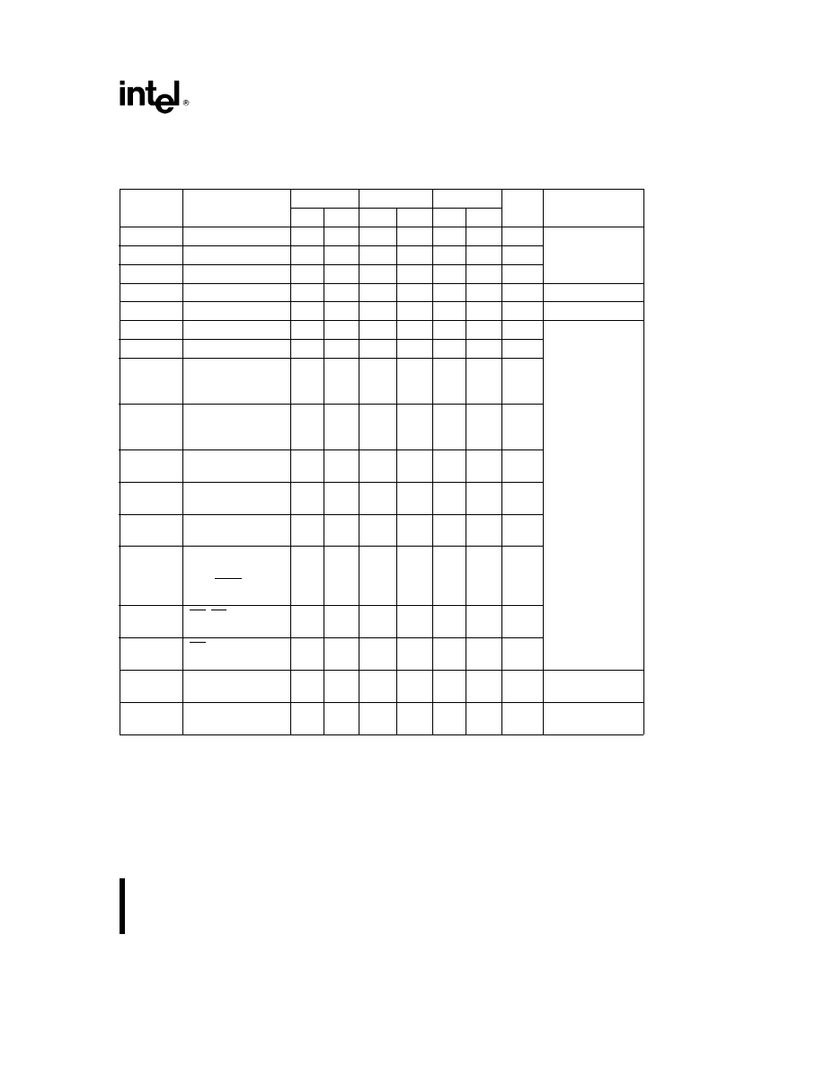
MINIMUM COMPLEXITY SYSTEM TIMING REQUIREMENTS
Symbol
Parameter
8086
8086-1
8086-2
Units
Test Conditions
Min
Max
Min
Max
Min
Max
TCLCL
CLK Cycle Period
200
500
100
500
125
500
ns
TCLCH
CLK Low Time
118
53
68
ns
TCHCL
CLK High Time
69
39
44
ns
TCH1CH2
CLK Rise Time
10
10
10
ns
From 1.0V to 3.5V
TCL2CL1
CLK Fall Time
10
10
10
ns
From 3.5V to 1.0V
TDVCL
Data in Setup Time
30
5
20
ns
TCLDX
Data in Hold Time
10
10
10
ns
TR1VCL
RDY Setup Time
35
35
35
ns
into 8284A (See
Notes 1, 2)
TCLR1X
RDY Hold Time
0
0
0
ns
into 8284A (See
Notes 1, 2)
TRYHCH
READY Setup
118
53
68
ns
Time into 8086
TCHRYX
READY Hold Time
30
20
20
ns
into 8086
TRYLCL
READY Inactive to
b
8
b
10
b
8
ns
CLK (See Note 3)
THVCH
HOLD Setup Time
35
20
20
ns
TINVCH
INTR, NMI, TEST
30
15
15
ns
Setup Time (See
Note 2)
TILIH
Input Rise Time
20
20
20
ns
From 0.8V to 2.0V
(Except CLK)
TIHIL
Input Fall Time
12
12
12
ns
From 2.0V to 0.8V
(Except CLK)
15
8086
A.C. CHARACTERISTICS
(Continued)
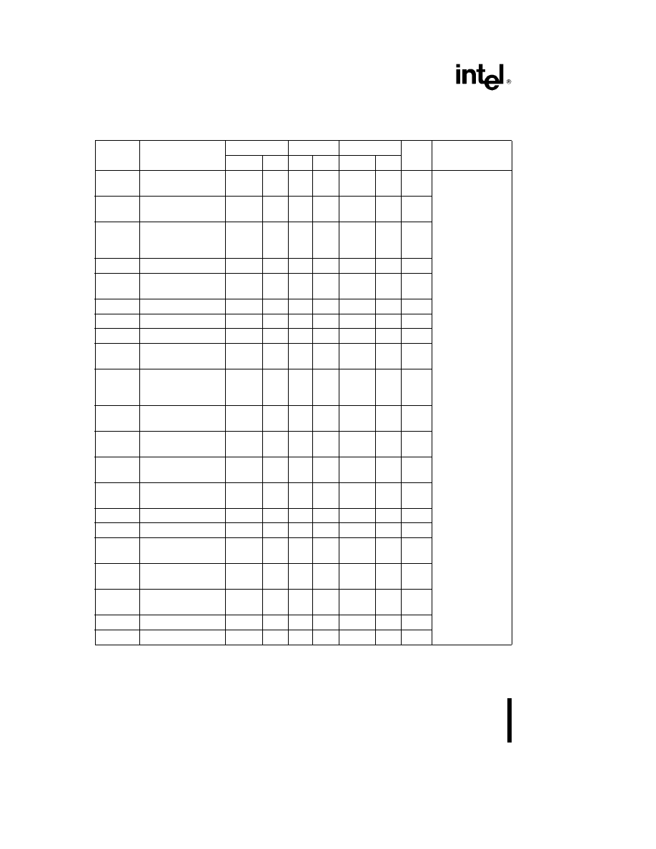
TIMING RESPONSES
Symbol
Parameter
8086
8086-1
8086-2
Units
Test
Min
Max
Min
Max
Min
Max
Conditions
TCLAV
Address Valid Delay
10
110
10
50
10
60
ns
TCLAX
Address Hold Time
10
10
10
ns
TCLAZ
Address Float
TCLAX
80
10
40
TCLAX
50
ns
Delay
TLHLL
ALE Width
TCLCH-20
TCLCH-10
TCLCH-10
ns
TCLLH
ALE Active Delay
80
40
50
ns
TCHLL
ALE Inactive Delay
85
45
55
ns
TLLAX
Address Hold Time
TCHCL-10
TCHCL-10
TCHCL-10
ns
TCLDV
Data Valid Delay
10
110
10
50
10
60
ns
*C
L
e
20–100 pF
for all 8086
TCHDX
Data Hold Time
10
10
10
ns
Outputs (In
addition to 8086
TWHDX Data Hold Time
TCLCH-30
TCLCH-25
TCLCH-30
ns
selfload)
After WR
TCVCTV Control Active
10
110
10
50
10
70
ns
Delay 1
TCHCTV Control Active
10
110
10
45
10
60
ns
Delay 2
TCVCTX Control Inactive
10
110
10
50
10
70
ns
Delay
TAZRL
Address Float to
0
0
0
ns
READ Active
TCLRL
RD Active Delay
10
165
10
70
10
100
ns
TCLRH
RD Inactive Delay
10
150
10
60
10
80
ns
TRHAV
RD Inactive to Next
TCLCL-45
TCLCL-35
TCLCL-40
ns
Address Active
TCLHAV HLDA Valid Delay
10
160
10
60
10
100
ns
TRLRH
RD Width
2TCLCL-75
2TCLCL-40
2TCLCL-50
ns
TWLWH WR Width
2TCLCL-60
2TCLCL-35
2TCLCL-40
ns
TAVAL
Address Valid to
TCLCH-60
TCLCH-35
TCLCH-40
ns
ALE Low
TOLOH
Output Rise Time
20
20
20
ns
From 0.8V to 2.0V
TOHOL
Output Fall Time
12
12
12
ns
From 2.0V to 0.8V
NOTES:
1. Signal at 8284A shown for reference only.
2. Setup requirement for asynchronous signal only to guarantee recognition at next CLK.
3. Applies only to T2 state. (8 ns into T3).
16
8086
A.C. TESTING INPUT, OUTPUT WAVEFORM
231455-11
A.C. Testing: Inputs are driven at 2.4V for a Logic ‘‘1’’ and 0.45V
for a Logic ‘‘0’’. Timing measurements are made at 1.5V for both
a Logic ‘‘1’’ and ‘‘0’’.
A.C. TESTING LOAD CIRCUIT
231455 – 12
C
L
Includes Jig Capacitance
WAVEFORMS
MINIMUM MODE
231455 – 13
17
8086
WAVEFORMS
(Continued)
MINIMUM MODE
(Continued)
231455 – 14
SOFTWARE HALTÐ
RD, WR, INTA e V
OH
DT/R e INDETERMINATE
NOTES:
1. All signals switch between V
OH
and V
OL
unless otherwise specified.
2. RDY is sampled near the end of T
2
, T
3
, T
W
to determine if T
W
machines states are to be inserted.
3. Two INTA cycles run back-to-back. The 8086 LOCAL ADDR/DATA BUS is floating during both INTA cycles. Control
signals shown for second INTA cycle.
4. Signals at 8284A are shown for reference only.
5. All timing measurements are made at 1.5V unless otherwise noted.
18
8086
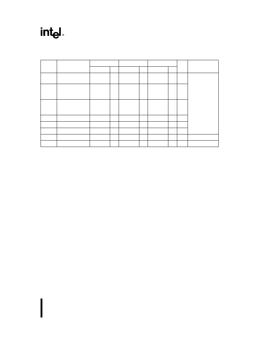
A.C. CHARACTERISTICS
MAX MODE SYSTEM (USING 8288 BUS CONTROLLER)
TIMING REQUIREMENTS
Symbol
Parameter
8086
8086-1
8086-2
Units
Test
Min
Max
Min
Max
Min
Max
Conditions
TCLCL
CLK Cycle Period
200
500
100
500
125
500
ns
TCLCH
CLK Low Time
118
53
68
ns
TCHCL
CLK High Time
69
39
44
ns
TCH1CH2
CLK Rise Time
10
10
10
ns
From 1.0V to 3.5V
TCL2CL1
CLK Fall Time
10
10
10
ns
From 3.5V to 1.0V
TDVCL
Data in Setup Time
30
5
20
ns
TCLDX
Data in Hold Time
10
10
10
ns
TR1VCL
RDY Setup Time
35
35
35
ns
into 8284A
(Notes 1, 2)
TCLR1X
RDY Hold Time
0
0
0
ns
into 8284A
(Notes 1, 2)
TRYHCH
READY Setup
118
53
68
ns
Time into 8086
TCHRYX
READY Hold Time
30
20
20
ns
into 8086
TRYLCL
READY Inactive to
b
8
b
10
b
8
ns
CLK (Note 4)
TINVCH
Setup Time for
30
15
15
ns
Recognition (INTR,
NMI, TEST)
(Note 2)
TGVCH
RQ/GT Setup Time
30
15
15
ns
(Note 5)
TCHGX
RQ Hold Time into
40
20
30
ns
8086
TILIH
Input Rise Time
20
20
20
ns
From 0.8V to 2.0V
(Except CLK)
TIHIL
Input Fall Time
12
12
12
ns
From 2.0V to 0.8V
(Except CLK)
19
8086
A.C. CHARACTERISTICS
(Continued)
TIMING RESPONSES
Symbol
Parameter
8086
8086-1
8086-2
Units
Test
Min
Max
Min
Max
Min
Max
Conditions
TCLML
Command Active
10
35
10
35
10
35
ns
Delay (See Note 1)
TCLMH
Command Inactive
10
35
10
35
10
35
ns
Delay (See Note 1)
TRYHSH
READY Active to
110
45
65
ns
Status Passive (See
Note 3)
TCHSV
Status Active Delay
10
110
10
45
10
60
ns
TCLSH
Status Inactive
10
130
10
55
10
70
ns
Delay
TCLAV
Address Valid Delay
10
110
10
50
10
60
ns
TCLAX
Address Hold Time
10
10
10
ns
TCLAZ
Address Float Delay
TCLAX
80
10
40
TCLAX
50
ns
TSVLH
Status Valid to ALE
15
15
15
ns
High (See Note 1)
TSVMCH
Status Valid to
15
15
15
ns
MCE High (See
Note 1)
TCLLH
CLK Low to ALE
15
15
15
ns
C
L
e
20 – 100 pF
for all 8086
Valid (See Note 1)
Outputs (In
TCLMCH
CLK Low to MCE
15
15
15
ns
addition to 8086
High (See Note 1)
self-load)
TCHLL
ALE Inactive Delay
15
15
15
ns
(See Note 1)
TCLMCL
MCE Inactive Delay
15
15
15
ns
(See Note 1)
TCLDV
Data Valid Delay
10
110
10
50
10
60
ns
TCHDX
Data Hold Time
10
10
10
ns
TCVNV
Control Active
5
45
5
45
5
45
ns
Delay (See Note 1)
TCVNX
Control Inactive
10
45
10
45
10
45
ns
Delay (See Note 1)
TAZRL
Address Float to
0
0
0
ns
READ Active
TCLRL
RD Active Delay
10
165
10
70
10
100
ns
TCLRH
RD Inactive Delay
10
150
10
60
10
80
ns
20
8086
A.C. CHARACTERISTICS
(Continued)
TIMING RESPONSES
(Continued)
Symbol
Parameter
8086
8086-1
8086-2
Units
Test
Min
Max
Min
Max
Min
Max
Conditions
TRHAV
RD Inactive to Next TCLCL-45
TCLCL-35
TCLCL-40
ns
Address Active
TCHDTL Direction Control
50
50
50
ns
C
L
e
20 – 100 pF
for all 8086
Active Delay
Outputs (In
(Note 1)
addition to 8086
TCHDTH Direction Control
30
30
30
ns
self-load)
Inactive Delay
(Note 1)
TCLGL
GT Active Delay
0
85
0
38
0
50
ns
TCLGH
GT Inactive Delay
0
85
0
45
0
50
ns
TRLRH
RD Width
2TCLCL-75
2TCLCL-40
2TCLCL-50
ns
TOLOH
Output Rise Time
20
20
20
ns
From 0.8V to 2.0V
TOHOL
Output Fall Time
12
12
12
ns
From 2.0V to 0.8V
NOTES:
1. Signal at 8284A or 8288 shown for reference only.
2. Setup requirement for asynchronous signal only to guarantee recognition at next CLK.
3. Applies only to T3 and wait states.
4. Applies only to T2 state (8 ns into T3).
21
8086
WAVEFORMS
MAXIMUM MODE
231455 – 15
22
8086
WAVEFORMS
(Continued)
MAXIMUM MODE
(Continued)
231455 – 16
NOTES:
1. All signals switch between V
OH
and V
OL
unless otherwise specified.
2. RDY is sampled near the end of T
2
, T
3
, T
W
to determine if T
W
machines states are to be inserted.
3. Cascade address is valid between first and second INTA cycle.
4. Two INTA cycles run back-to-back. The 8086 LOCAL ADDR/DATA BUS is floating during both INTA cycles. Control for
pointer address is shown for second INTA cycle.
5. Signals at 8284A or 8288 are shown for reference only.
6. The issuance of the 8288 command and control signals (MRDC, MWTC, AMWC, IORC, IOWC, AIOWC, INTA and DEN)
lags the active high 8288 CEN.
7. All timing measurements are made at 1.5V unless otherwise noted.
8. Status inactive in state just prior to T
4
.
23
8086
WAVEFORMS
(Continued)
ASYNCHRONOUS SIGNAL RECOGNITION
231455 – 17
NOTE:
1. Setup requirements for asynchronous signals only to guarantee recognition at next CLK.
BUS LOCK SIGNAL TIMING (MAXIMUM MODE
ONLY)
231455 – 18
RESET TIMING
231455 – 19
REQUEST/GRANT SEQUENCE TIMING (MAXIMUM MODE ONLY)
231455 – 20
NOTE:
The coprocessor may not drive the buses outside the region shown without risking contention.
24
8086
WAVEFORMS
(Continued)
HOLD/HOLD ACKNOWLEDGE TIMING (MINIMUM MODE ONLY)
231455 – 21
25
8086
Table 2. Instruction Set Summary
Mnemonic and
Instruction Code
Description
DATA TRANSFER
MOV e Move:
7 6 5 4 3 2 1 0
7 6 5 4 3 2 1 0
7 6 5 4 3 2 1 0
7 6 5 4 3 2 1 0
Register/Memory to/from Register
1 0 0 0 1 0 d w
mod
reg
r/m
Immediate to Register/Memory
1 1 0 0 0 1 1 w
mod 0 0 0 r/m
data
data if w e 1
Immediate to Register
1 0 1 1 w reg
data
data if w e 1
Memory to Accumulator
1 0 1 0 0 0 0 w
addr-low
addr-high
Accumulator to Memory
1 0 1 0 0 0 1 w
addr-low
addr-high
Register/Memory to Segment Register
1 0 0 0 1 1 1 0
mod 0 reg r/m
Segment Register to Register/Memory
1 0 0 0 1 1 0 0
mod 0 reg r/m
PUSH e Push:
Register/Memory
1 1 1 1 1 1 1 1
mod 1 1 0 r/m
Register
0 1 0 1 0 reg
Segment Register
0 0 0 reg 1 1 0
POP e Pop:
Register/Memory
1 0 0 0 1 1 1 1
mod 0 0 0 r/m
Register
0 1 0 1 1 reg
Segment Register
0 0 0 reg 1 1 1
XCHG e Exchange:
Register/Memory with Register
1 0 0 0 0 1 1 w
mod reg r/m
Register with Accumulator
1 0 0 1 0 reg
IN e Input from:
Fixed Port
1 1 1 0 0 1 0 w
port
Variable Port
1 1 1 0 1 1 0 w
OUT e Output to:
Fixed Port
1 1 1 0 0 1 1 w
port
Variable Port
1 1 1 0 1 1 1 w
XLAT e
Translate Byte to AL
1 1 0 1 0 1 1 1
LEA e
Load EA to Register
1 0 0 0 1 1 0 1
mod reg r/m
LDS e
Load Pointer to DS
1 1 0 0 0 1 0 1
mod reg r/m
LES e
Load Pointer to ES
1 1 0 0 0 1 0 0
mod reg r/m
LAHF e
Load AH with Flags
1 0 0 1 1 1 1 1
SAHF e
Store AH into Flags
1 0 0 1 1 1 1 0
PUSHF e
Push Flags
1 0 0 1 1 1 0 0
POPF e
Pop Flags
1 0 0 1 1 1 0 1
Mnemonics
©
Intel, 1978
26
8086
Table 2. Instruction Set Summary
(Continued)
Mnemonic and
Instruction Code
Description
ARITHMETIC
7 6 5 4 3 2 1 0
7 6 5 4 3 2 1 0
7 6 5 4 3 2 1 0
7 6 5 4 3 2 1 0
ADD e Add:
Reg./Memory with Register to Either
0 0 0 0 0 0 d w
mod reg r/m
Immediate to Register/Memory
1 0 0 0 0 0 s w
mod 0 0 0 r/m
data
data if s: w e 01
Immediate to Accumulator
0 0 0 0 0 1 0 w
data
data if w e 1
ADC e Add with Carry:
Reg./Memory with Register to Either
0 0 0 1 0 0 d w
mod reg r/m
Immediate to Register/Memory
1 0 0 0 0 0 s w
mod 0 1 0 r/m
data
data if s: w e 01
Immediate to Accumulator
0 0 0 1 0 1 0 w
data
data if w e 1
INC e Increment:
Register/Memory
1 1 1 1 1 1 1 w
mod 0 0 0 r/m
Register
0 1 0 0 0 reg
AAA e
ASCII Adjust for Add
0 0 1 1 0 1 1 1
BAA e
Decimal Adjust for Add
0 0 1 0 0 1 1 1
SUB e Subtract:
Reg./Memory and Register to Either
0 0 1 0 1 0 d w
mod reg r/m
Immediate from Register/Memory
1 0 0 0 0 0 s w
mod 1 0 1 r/m
data
data if s w e 01
Immediate from Accumulator
0 0 1 0 1 1 0 w
data
data if w e 1
SSB e Subtract with Borrow
Reg./Memory and Register to Either
0 0 0 1 1 0 d w
mod reg r/m
Immediate from Register/Memory
1 0 0 0 0 0 s w
mod 0 1 1 r/m
data
data if s w e 01
Immediate from Accumulator
0 0 0 1 1 1 w
data
data if w e 1
DEC e Decrement:
Register/memory
1 1 1 1 1 1 1 w
mod 0 0 1 r/m
Register
0 1 0 0 1 reg
NEG e
Change sign
1 1 1 1 0 1 1 w
mod 0 1 1 r/m
CMP e Compare:
Register/Memory and Register
0 0 1 1 1 0 d w
mod reg r/m
Immediate with Register/Memory
1 0 0 0 0 0 s w
mod 1 1 1 r/m
data
data if s w e 01
Immediate with Accumulator
0 0 1 1 1 1 0 w
data
data if w e 1
AAS e
ASCII Adjust for Subtract
0 0 1 1 1 1 1 1
DAS e
Decimal Adjust for Subtract
0 0 1 0 1 1 1 1
MUL e
Multiply (Unsigned)
1 1 1 1 0 1 1 w
mod 1 0 0 r/m
IMUL e
Integer Multiply (Signed)
1 1 1 1 0 1 1 w
mod 1 0 1 r/m
AAM e
ASCII Adjust for Multiply
1 1 0 1 0 1 0 0
0 0 0 0 1 0 1 0
DIV e
Divide (Unsigned)
1 1 1 1 0 1 1 w
mod 1 1 0 r/m
IDIV e
Integer Divide (Signed)
1 1 1 1 0 1 1 w
mod 1 1 1 r/m
AAD e
ASCII Adjust for Divide
1 1 0 1 0 1 0 1
0 0 0 0 1 0 1 0
CBW e
Convert Byte to Word
1 0 0 1 1 0 0 0
CWD e
Convert Word to Double Word
1 0 0 1 1 0 0 1
Mnemonics
©
Intel, 1978
27
8086
Table 2. Instruction Set Summary
(Continued)
Mnemonic and
Instruction Code
Description
LOGIC
7 6 5 4 3 2 1 0
7 6 5 4 3 2 1 0
7 6 5 4 3 2 1 0
7 6 5 4 3 2 1 0
NOT e
Invert
1 1 1 1 0 1 1 w
mod 0 1 0 r/m
SHL/SAL e
Shift Logical/Arithmetic Left
1 1 0 1 0 0 v w
mod 1 0 0 r/m
SHR e
Shift Logical Right
1 1 0 1 0 0 v w
mod 1 0 1 r/m
SAR e
Shift Arithmetic Right
1 1 0 1 0 0 v w
mod 1 1 1 r/m
ROL e
Rotate Left
1 1 0 1 0 0 v w
mod 0 0 0 r/m
ROR e
Rotate Right
1 1 0 1 0 0 v w
mod 0 0 1 r/m
RCL e
Rotate Through Carry Flag Left
1 1 0 1 0 0 v w
mod 0 1 0 r/m
RCR e
Rotate Through Carry Right
1 1 0 1 0 0 v w
mod 0 1 1 r/m
AND e And:
Reg./Memory and Register to Either
0 0 1 0 0 0 d w
mod reg r/m
Immediate to Register/Memory
1 0 0 0 0 0 0 w
mod 1 0 0 r/m
data
data if w e 1
Immediate to Accumulator
0 0 1 0 0 1 0 w
data
data if w e 1
TEST e And Function to Flags, No Result:
Register/Memory and Register
1 0 0 0 0 1 0 w
mod reg r/m
Immediate Data and Register/Memory
1 1 1 1 0 1 1 w
mod 0 0 0 r/m
data
data if w e 1
Immediate Data and Accumulator
1 0 1 0 1 0 0 w
data
data if w e 1
OR e Or:
Reg./Memory and Register to Either
0 0 0 0 1 0 d w
mod reg r/m
Immediate to Register/Memory
1 0 0 0 0 0 0 w
mod 0 0 1 r/m
data
data if w e 1
Immediate to Accumulator
0 0 0 0 1 1 0 w
data
data if w e 1
XOR e Exclusive or:
Reg./Memory and Register to Either
0 0 1 1 0 0 d w
mod reg r/m
Immediate to Register/Memory
1 0 0 0 0 0 0 w
mod 1 1 0 r/m
data
data if w e 1
Immediate to Accumulator
0 0 1 1 0 1 0 w
data
data if w e 1
STRING MANIPULATION
REP e
Repeat
1 1 1 1 0 0 1 z
MOVS e
Move Byte/Word
1 0 1 0 0 1 0 w
CMPS e
Compare Byte/Word
1 0 1 0 0 1 1 w
SCAS e
Scan Byte/Word
1 0 1 0 1 1 1 w
LODS e
Load Byte/Wd to AL/AX
1 0 1 0 1 1 0 w
STOS e
Stor Byte/Wd from AL/A
1 0 1 0 1 0 1 w
CONTROL TRANSFER
CALL e Call:
Direct within Segment
1 1 1 0 1 0 0 0
disp-low
disp-high
Indirect within Segment
1 1 1 1 1 1 1 1
mod 0 1 0 r/m
Direct Intersegment
1 0 0 1 1 0 1 0
offset-low
offset-high
seg-low
seg-high
Indirect Intersegment
1 1 1 1 1 1 1 1
mod 0 1 1 r/m
Mnemonics
©
Intel, 1978
28
8086
Table 2. Instruction Set Summary
(Continued)
Mnemonic and
Instruction Code
Description
JMP e Unconditional Jump:
7 6 5 4 3 2 1 0
7 6 5 4 3 2 1 0
7 6 5 4 3 2 1 0
Direct within Segment
1 1 1 0 1 0 0 1
disp-low
disp-high
Direct within Segment-Short
1 1 1 0 1 0 1 1
disp
Indirect within Segment
1 1 1 1 1 1 1 1
mod 1 0 0 r/m
Direct Intersegment
1 1 1 0 1 0 1 0
offset-low
offset-high
seg-low
seg-high
Indirect Intersegment
1 1 1 1 1 1 1 1
mod 1 0 1 r/m
RET e Return from CALL:
Within Segment
1 1 0 0 0 0 1 1
Within Seg Adding Immed to SP
1 1 0 0 0 0 1 0
data-low
data-high
Intersegment
1 1 0 0 1 0 1 1
Intersegment Adding Immediate to SP
1 1 0 0 1 0 1 0
data-low
data-high
JE/JZ e
Jump on Equal/Zero
0 1 1 1 0 1 0 0
disp
JL/JNGE e
Jump on Less/Not Greater
0 1 1 1 1 1 0 0
disp
or Equal
JLE/JNG e
Jump on Less or Equal/
0 1 1 1 1 1 1 0
disp
Not Greater
JB/JNAE e
Jump on Below/Not Above
0 1 1 1 0 0 1 0
disp
or Equal
JBE/JNA e
Jump on Below or Equal/
0 1 1 1 0 1 1 0
disp
Not Above
JP/JPE e
Jump on Parity/Parity Even
0 1 1 1 1 0 1 0
disp
JO e
Jump on Overflow
0 1 1 1 0 0 0 0
disp
JS e
Jump on Sign
0 1 1 1 1 0 0 0
disp
JNE/JNZ e
Jump on Not Equal/Not Zero
0 1 1 1 0 1 0 1
disp
JNL/JGE e
Jump on Not Less/Greater
0 1 1 1 1 1 0 1
disp
or Equal
JNLE/JG e
Jump on Not Less or Equal/
0 1 1 1 1 1 1 1
disp
Greater
JNB/JAE e
Jump on Not Below/Above
0 1 1 1 0 0 1 1
disp
or Equal
JNBE/JA e
Jump on Not Below or
0 1 1 1 0 1 1 1
disp
Equal/Above
JNP/JPO e
Jump on Not Par/Par Odd
0 1 1 1 1 0 1 1
disp
JNO e
Jump on Not Overflow
0 1 1 1 0 0 0 1
disp
JNS e
Jump on Not Sign
0 1 1 1 1 0 0 1
disp
LOOP e
Loop CX Times
1 1 1 0 0 0 1 0
disp
LOOPZ/LOOPE e
Loop While Zero/Equal
1 1 1 0 0 0 0 1
disp
LOOPNZ/LOOPNE e
Loop While Not
1 1 1 0 0 0 0 0
disp
Zero/Equal
JCXZ e
Jump on CX Zero
1 1 1 0 0 0 1 1
disp
INT e Interrupt
Type Specified
1 1 0 0 1 1 0 1
type
Type 3
1 1 0 0 1 1 0 0
INTO e
Interrupt on Overflow
1 1 0 0 1 1 1 0
IRET e
Interrupt Return
1 1 0 0 1 1 1 1
29
8086
Table 2. Instruction Set Summary
(Continued)
Mnemonic and
Instruction Code
Description
7 6 5 4 3 2 1 0
7 6 5 4 3 2 1 0
PROCESSOR CONTROL
CLC e
Clear Carry
1 1 1 1 1 0 0 0
CMC e
Complement Carry
1 1 1 1 0 1 0 1
STC e
Set Carry
1 1 1 1 1 0 0 1
CLD e
Clear Direction
1 1 1 1 1 1 0 0
STD e
Set Direction
1 1 1 1 1 1 0 1
CLI e
Clear Interrupt
1 1 1 1 1 0 1 0
STI e
Set Interrupt
1 1 1 1 1 0 1 1
HLT e
Halt
1 1 1 1 0 1 0 0
WAIT e
Wait
1 0 0 1 1 0 1 1
ESC e
Escape (to External Device)
1 1 0 1 1 x x x
mod x x x r/m
LOCK e
Bus Lock Prefix
1 1 1 1 0 0 0 0
NOTES:
AL
e
8-bit accumulator
AX
e
16-bit accumulator
CX
e
Count register
DS
e
Data segment
ES
e
Extra segment
Above/below refers to unsigned value
Greater
e
more positive;
Less
e
less positive (more negative) signed values
if d
e
1 then ‘‘to’’ reg; if d
e
0 then ‘‘from’’ reg
if w
e
1 then word instruction; if w
e
0 then byte instruc-
tion
if mod
e
11 then r/m is treated as a REG field
if mod
e
00 then DISP
e
0*, disp-low and disp-high are
absent
if mod
e
01 then DISP
e
disp-low sign-extended to
16 bits, disp-high is absent
if mod
e
10 then DISP
e
disp-high; disp-low
if r/m
e
000 then EA
e
(BX)
a
(SI)
a
DISP
if r/m
e
001 then EA
e
(BX)
a
(DI)
a
DISP
if r/m
e
010 then EA
e
(BP)
a
(SI)
a
DISP
if r/m
e
011 then EA
e
(BP)
a
(DI)
a
DISP
if r/m
e
100 then EA
e
(SI)
a
DISP
if r/m
e
101 then EA
e
(DI)
a
DISP
if r/m
e
110 then EA
e
(BP)
a
DISP*
if r/m
e
111 then EA
e
(BX)
a
DISP
DISP follows 2nd byte of instruction (before data if re-
quired)
*except if mod
e
00 and r/m
e
110 then EA
e
disp-high;
disp-low.
Mnemonics
©
Intel, 1978
if s w
e
01 then 16 bits of immediate data form the oper-
and
if s w
e
11 then an immediate data byte is sign extended
to form the 16-bit operand
if v
e
0 then ‘‘count’’
e
1; if v
e
1 then ‘‘count’’ in (CL)
x
e
don’t care
z is used for string primitives for comparison with ZF FLAG
SEGMENT OVERRIDE PREFIX
0 0 1 reg 1 1 0
REG is assigned according to the following table:
16-Bit (w e 1)
8-Bit (w e 0)
Segment
000
AX
000
AL
00
ES
001
CX
001
CL
01
CS
010
DX
010
DL
10
SS
011
BX
011
BL
11
DS
100
SP
100
AH
101
BP
101
CH
110
SI
110
DH
111
DI
111
BH
Instructions which reference the flag register file as a 16-bit
object use the symbol FLAGS to represent the file:
FLAGS e X:X:X:X:(OF):(DF):(IF):(TF):(SF):(ZF):X:(AF):X:(PF):X:(CF)
DATA SHEET REVISION REVIEW
The following list represents key differences between this and the -004 data sheet. Please review this summa-
ry carefully.
1. The Intel 8086 implementation technology (HMOS) has been changed to (HMOS-III).
2. Delete all ‘‘changes from 1985 Handbook Specification’’ sentences.
30
Wyszukiwarka
Podobne podstrony:
8086
8086
CW 05 B 8086 2 fsyst
Procesor 8086
09 kompresja pasy nasuwcze na szelfachid 8086 ppt
8086
procesor 8086
Procesor 8086, POLITECHNIKA wydział E kierunek I, ARCHITEKTURA SYSTEMOW KOMPUTEROWYCH
8086
[cwiczenie] #2 8086, zadania
Procesor 8086
8086 Lista rozkazów, Akademia Morska, III semestr, technika cyfrowa, Technika Cyfrowa, TC - lab Dąbr
8086
8086
CW 04 B 8086 1
architektura procesora [1] materialy 8086 1
8086
8086
więcej podobnych podstron