
PSoC Designer
™
:
User Guide
Cypress MicroSystems, Inc.
2700 162nd St. SW, Building D
Lynnwood, WA 98037
Phone: 800.669.0557
Fax: 425.787.4641
Document #: 38-12004 Rev. *B
Last Revised: August 12, 2004
Assembly Language

http://www.cypress.com/ http://www.cypress.com/aboutus/sales_locations.cfm
http://www.cypress.com/support/mysupport.cfm
Copyright © 2001-2004 Cypress MicroSystems, Inc. All rights reserved.
PSoC™, Programmable System-on-Chip™, and PSoC Designer™ are trademarks of
Cypress MicroSystems, Inc.
All other trademarks or registered trademarks referenced herein are the property of their respective
owners. The information contained herein is subject to change without notice. Made in the U.S.A.
The software is owned by Cypress MicroSystems, Inc. (CMS) and is protected by and subject to world-
wide patent protection (United States and foreign), United States copyright laws and international treaty
provisions. Therefore, unless otherwise specified in a separate license agreement between you and
CMS, this software must be treated like any other copyrighted material. Reproduction, modification,
translation, compilation, or representation of this software in any other form (e.g., paper, magnetic,
optical, silicon, etc.) is prohibited without CMS’ express written permission.
Disclaimer: CMS MAKES NO WARRANTY OF ANY KIND, EXPRESS OR IMPLIED, WITH REGARD TO
THIS MATERIAL, INCLUDING, BUT NOT LIMITED TO, THE IMPLIED WARRANTIES OF MERCHANT-
ABILITY AND FITNESS FOR A PARTICULAR PURPOSE. CMS reserves the right to make changes
without further notice to the materials described herein. CMS does not assume any liability arising out of
the application or use of any product or circuit described herein. CMS does not authorize its products for
use as critical components in life-support systems where a malfunction or failure may reasonably be
expected to result in significant injury to the user. The inclusion of CMS’ product in a life-support systems
application implies that the manufacturer assumes all risk of such use and in doing so indemnifies CMS
against all charges.

August 12, 2004
Document #: 38-12004 Rev. *B
3
List of Tables ................................................................................................. 7
Notation Standards ....................................................................................... 9
Section 1. Introduction ............................................................................... 11
1.1 Purpose .....................................................................................................................11
1.2 Section Overview .......................................................................................................11
1.3 Product Updates ........................................................................................................12
1.4 Support ......................................................................................................................12
Section 2. The M8C Microprocessor ......................................................... 13
2.1 Introduction ................................................................................................................13
2.2 Internal Registers ......................................................................................................13
2.3 Address Spaces ........................................................................................................14
2.4 Instruction Format ......................................................................................................15
2.4.1 One-Byte Instructions .......................................................................................16
2.4.2 Two-Byte Instructions .......................................................................................16
2.4.3 Three-Byte Instructions ....................................................................................17
2.5.1 Source Immediate ............................................................................................19
2.5.2 Source Direct ...................................................................................................19
2.5.3 Source Indexed ................................................................................................20
2.5.4 Destination Direct .............................................................................................20
2.5.5 Destination Indexed .........................................................................................21
2.5.6 Destination Direct Source Immediate ...............................................................21
2.5.7 Destination Indexed Source Immediate ...........................................................21
2.5.8 Destination Direct Source Direct ......................................................................22
2.5.9 Source Indirect Post Increment ........................................................................22
2.5.10 Destination Indirect Post Increment ...............................................................23
Section 3. The PSoC Designer Assembler ............................................... 25
3.1.1 Labels ...............................................................................................................26
3.1.2 Mnemonics .......................................................................................................27
3.1.3 Operands .........................................................................................................28
3.1.4 Comments ........................................................................................................29
3.1.5 Directives .........................................................................................................30
3.2 Listing File Format .....................................................................................................30
3.3 Map File Format ........................................................................................................30
3.4 ROM File Format .......................................................................................................31
3.5 Intel® HEX File Format ..............................................................................................31
3.6 Convention for Restoring Internal Registers ..............................................................34
3.7 Compiling a File into a Library Module ......................................................................35
Table of Contents

PSoC Designer: Assembly Language User Guide
4
Document #: 38-12004 Rev. *B
August 12, 2004
Section 4. M8C Instruction Set .................................................................. 39
4.1 Add with Carry ................................................................................................... ADC 40
4.2 Add without Carry .............................................................................................. ADD 41
4.3 Bitwise AND....................................................................................................... AND 42
4.4 Arithmetic Shift Left ........................................................................................... ASL 43
4.5 Arithmetic Shift Right ......................................................................................... ASR 44
4.6 Call Function.....................................................................................................CALL 45
4.7 Non-destructive Compare..................................................................................CMP 46
4.8 Complement Accumulator ..................................................................................CPL 46
4.9 Decrement ......................................................................................................... DEC 47
4.10 Halt .................................................................................................................HALT 47
4.11 Increment...........................................................................................................INC 48
4.12 Relative Table Read .....................................................................................INDEX 49
4.13 Jump Accumulator ......................................................................................... JACC 50
4.14 Jump if Carry ...................................................................................................... JC 51
4.15 Jump.................................................................................................................JMP 52
4.16 Jump if No Carry...............................................................................................JNC 53
4.17 Jump if Not Zero ............................................................................................... JNZ 54
4.18 Jump if Zero.........................................................................................................JZ 55
4.19 Long Call ......................................................................................................LCALL 56
4.20 Long Jump......................................................................................................LJMP 57
4.21 Move................................................................................................................MOV 58
4.22 Move Indirect, Post-Increment to Memory........................................................ MVI 59
4.23 No Operation ................................................................................................... NOP 60
4.24 Bitwise OR......................................................................................................... OR 61
4.25 Pop Stack into Register ................................................................................... POP 62
4.26 Push Register onto Stack ..............................................................................PUSH 63
4.27 Return...............................................................................................................RET 64
4.28 Return from Interrupt ......................................................................................RETI 65
4.29 Rotate Left through Carry ................................................................................RLC 66
4.30 Absolute Table Read ................................................................................... ROMX 67
4.31 Rotate Right through Carry ............................................................................. RRC 68
4.32 Subtract with Borrow ........................................................................................SBB 69
4.33 Subtract without Borrow ................................................................................. SUB 70
4.34 Swap............................................................................................................. SWAP 71
4.35 System Supervisor Call .................................................................................. SSC 72
4.36 Test with Mask.................................................................................................. TST 73
4.37 Bitwise XOR .................................................................................................... XOR 74

August 12, 2004
Document #: 38-12004 Rev. *B
5
Section 5. Assembler Directives ............................................................... 77
5.14 Prevent Code Compression of Data ............................... .LITERAL, .ENDLITERAL 86
5.17 Section for Dead-Code Elimination ............................. .SECTION, .ENDSECTION 88
5.18 Suspend and Resume Code Compressor ..................................Suspend - OR F,0 89
Section 6. Compile/Assemble Error Messages ........................................ 91
6.1 Linker Operations ......................................................................................................91
6.2 Preprocessor Errors ..................................................................................................92
6.3 Assembler Errors .......................................................................................................94
6.4 Linker Errors ..............................................................................................................95
6.5 Code Compressor and Dead-Code Elimination Error Messages ..............................95
Appendix A. Assembly Language Reference Tables .............................. 97
Index .......................................................................................................... 101

PSoC Designer: Assembly Language User Guide
6
Document #: 38-12004 Rev. *B
August 12, 2004

August 12, 2004
Document #: 38-12004 Rev. *B
7
Table 1: Internal Registers............................................................................................................ 9
Table 2: Flag (F) Register ........................................................................................................... 14
Table 3: One-Byte Instruction Format......................................................................................... 16
Table 4: Two-Byte Instruction Formats ....................................................................................... 17
Table 5: Three-Byte Instruction Formats .................................................................................... 18
Table 6: Source Immediate......................................................................................................... 19
Table 7: Source Direct ................................................................................................................ 19
Table 8: Source Indexed............................................................................................................. 20
Table 9: Destination Direct.......................................................................................................... 20
Table 10: Destination Indexed .................................................................................................... 21
Table 11: Destination Direct Source Immediate ......................................................................... 21
Table 12: Destination Indexed Source Immediate ...................................................................... 22
Table 13: Destination Direct Source Direct................................................................................. 22
Table 14: Source Indirect Post Increment................................................................................... 23
Table 15: Destination Indirect Post Increment ............................................................................ 23
Table 16: Five Basic Components of an Assembly Source File ................................................. 25
Table 17: Constants Formats...................................................................................................... 28
Table 18: Register Formats ........................................................................................................ 29
Table 19: RAM Format................................................................................................................ 29
Table 20: Expressions ................................................................................................................ 29
Table 21: Intel HEX File Record Format ..................................................................................... 32
Table 22: PSoC Microcontroller Intel HEX File Format............................................................... 33
Table 23: Preprocessor Errors/Warnings.................................................................................... 92
Table 24: Preprocessor Command Line Errors .......................................................................... 93
Table 25: Assembler Errors/Warnings ........................................................................................ 94
Table 26: Assembler Command Line Errors/Warnings............................................................... 95
Table 27: Linker Errors/Warnings ............................................................................................... 95
Table A-1: Documentation Conventions ..................................................................................... 97
Table A-3: Assembly Syntax Expressions .................................................................................. 98
Table A-2: Instruction Set Summary (Sorted by Mnemonic)....................................................... 98
Table A-4: Instruction Set Summary (Sorted by Opcode)........................................................... 99
Table A-5: Assembler Directives Summary .............................................................................. 100
Table A-6: ASCII Code Table ................................................................................................... 100
List of Tables

PSoC Designer: Assembly Language User Guide
8
Document #: 38-12004 Rev. *B
August 12, 2004

August 12, 2004
Document #: 38-12004 Rev. *B
9
Following is input notation referenced throughout this guide and wherever
applicable in the PSoC Designer suite of product documentation.
Notation Standards
Table 1:
Internal Registers
Notation
Description
A
Accumulator
CF
Carry Flag
expr
Expression
F
Flags (ZF, CF, and Others)
k
Operand 1 Value
k
1
k
2
First Operand of 2 Operands
Second Operand of 2 Operands
PC
Program Counter
SP
Stack Pointer
X
X Register
ZF
Zero Flag
REG
Register Space

PSoC Designer: Assembly Language User Guide
10
Document #: 38-12004 Rev. *B
August 12, 2004

Section 1. Introduction
August 12, 2004
Document #: 38-12004 Rev. *B
11
1.1
Purpose
The PSoC Designer: Assembly Language User Guide documents the assem-
bly language instruction set for the M8C microprocessor as well as other com-
patible assembly practices.
The PSoC Designer Integrated Development Environment software is avail-
able free of charge and supports development in assembly language. For cus-
tomers interested in developing in ‘C’, a low-cost compiler is available. Please
contact your local distributor if you are interested in purchasing the C compiler
for PSoC Designer. For more information about developing in C for the PSoC
device, please read the PSoC Designer: C Language Compiler User Guide
available at the Cypress web site.
1.2
Section Overview
Following is a brief description of each section in this user guide:
Section 1. Introduction
Discusses the microprocessor and
explains address spaces, instruction for-
mat, and destination of instruction results.
It also lists all addressing modes with
examples.
Provides assembly-language-source syn-
tax including labels, mnemonics, oper-
ands, expressions, and comments.
Provides a detailed list of all instructions.
Provides a detailed list of all directives.
Provides several lists of compile/assem-
bler-related errors and warnings.

PSoC Designer: Assembly Language User Guide
12
Document #: 38-12004 Rev. *B
August 12, 2004
1.3
Product Updates
The Cypress web site (
date information available about Cypress MicroSystems products. Please visit
the web site for the latest version of PSoC Designer, the industry leading soft-
ware development tool for PSoC devices. PSoC Designer is provided free of
charge. You may also order PSoC Designer on CD-ROM by contacting your
local distributor.
1.4
Support
Support for Cypress MicroSystems products is available free at
. Resources include User Discussion Forums, Application
Notes, CYPros Consultants listing, TightLink Technical Support Email/Knowl-
edge Base, Tele-Training seminars, and contact information for Support Tech-
nicians.
Cypress MicroSystems was established as a subsidiary of Cypress Semicon-
ductor Corporation (NYSE: CY) in the fourth quarter of 1999. PSoC-related
support is also available at

Section 2. The M8C Microprocessor
August 12, 2004
Document #: 38-12004 Rev. *B
13
2.1
Introduction
The M8C is a 4 MIPS 8-bit Harvard architecture microprocessor. Code select-
able processor clock speeds from 93.7 kHz to 24 MHz allow the M8C to be
tuned to a particular application’s performance and power requirements. The
M8C supports a rich instruction set which allows for efficient low-level lan-
guage support.
This section covers:
Internal M8C Registers
Address Spaces
Instruction Formats
Addressing Modes
2.2
Internal Registers
The M8C has five internal registers that are used in program execution. Fol-
lowing is a list of the registers:
Accumulator (
A
)
Index (
X
)
Program Counter (
PC
)
Stack Pointer (
SP
)
Flags (
F
)
All of the internal M8C registers are 8-bits in width except for the
PC
which is
16-bits wide. Upon reset,
A
,
X
,
PC
, and
SP
are reset to
0x00.
The Flag register
(
F
) is reset to
0x02
indicating that the
Z
flag is set.
With each stack operation, the
SP
is automatically incremented or decre-
mented so that it always points at the next stack byte in RAM. If the last byte in
the stack is at address
0xFF
in RAM, the Stack Pointer will wrap to RAM
Section 2. The M8C Microprocessor

PSoC Designer: Assembly Language User Guide
14
Document #: 38-12004 Rev. *B
August 12, 2004
address
0x00
. It is the firmware developer’s responsibility to ensure that the
stack does not overlap with user-defined variables in RAM.
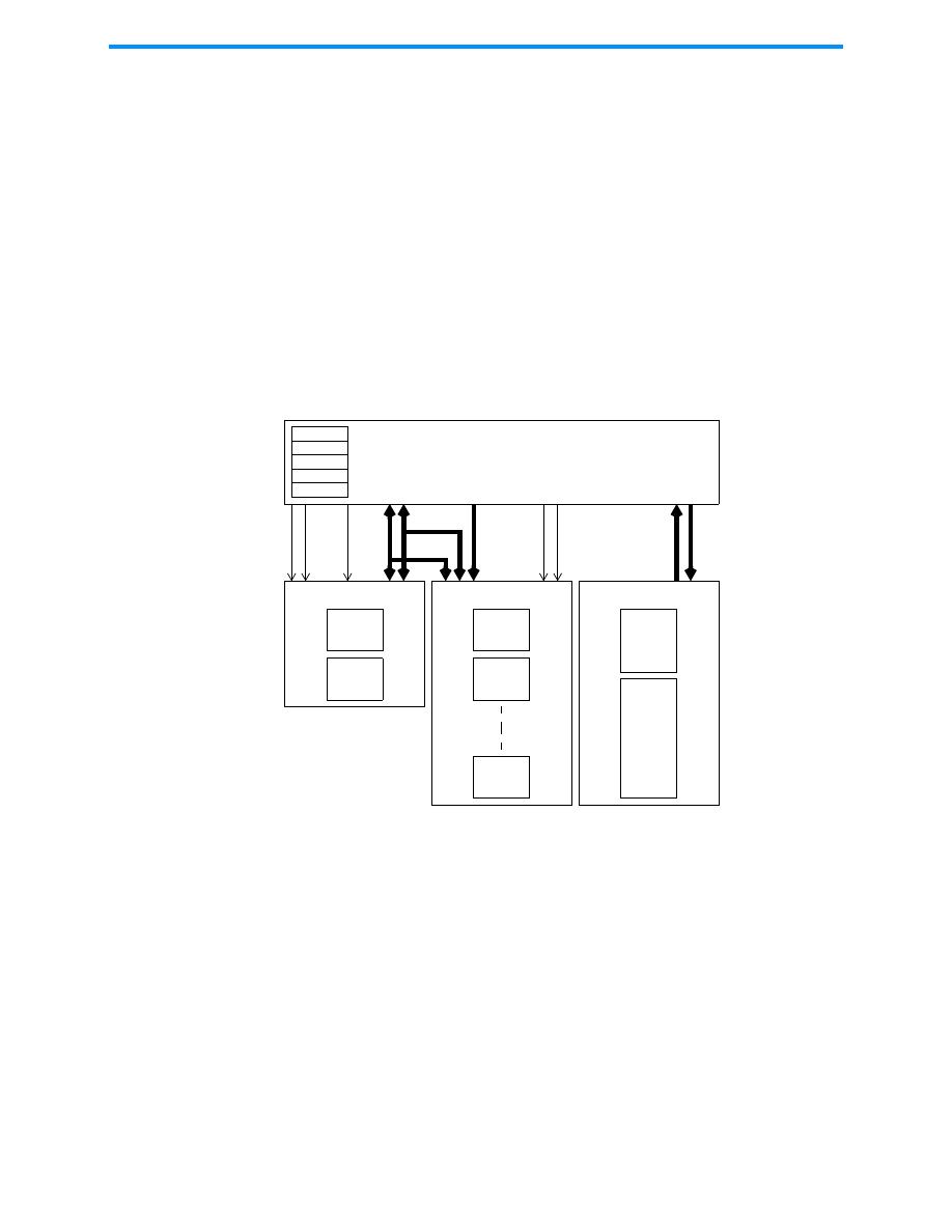
As shown in
, the Flag register has 6 of 8 bits defined. The
PgMode
and
XIO
bits are used to control the active register and RAM address
spaces in the PSoC device. The C and Z bits are the Carry and Zero flags
respectively. These flags are affected by arithmetic, logical, and shift opera-
tions provided in the M8C instruction. The GIE bit is the Global Interrupt
Enable. When set, this bit allows the M8C to be interrupted by the PSoC
device’s interrupt controller.
With the exception of the
F
register, the M8C internal registers are not accessi-
ble via an explicit register address. PSoC parts in the CY8C25xxx and
CY8C26xxx device family do not have a readable
F
register. The
OR F, expr
and
AND F, expr
instructions must be used to set and clear
F
register bits. The
internal M8C registers are accessed using special instructions such as:
MOV A, expr
MOV X, expr
SWAP A, SP
OR F, expr
JMP
The
F
register may be read by using address
0xF7
in any register bank, except
in CY8C25xxx and CY8C26xxx devices.
2.3
Address Spaces
The M8C microcontroller has three address spaces: ROM, RAM, and regis-
ters. The ROM address space is accessed via its own address and data bus.
illustrates the arrangement of the PSoC device address spaces.
The ROM address space is composed of the Supervisory ROM and the on-
chip Flash program store. Flash is organized into 64-byte blocks. The user
need not be concerned with program store page boundaries, as the M8C auto-
matically increments the 16-bit
PC
on every instruction making the block
boundaries invisible to user code. Instructions occurring on a 256-byte Flash
page boundary (with the exception of
jump
instructions) incur an extra M8C
clock cycle as the upper byte of the
PC
is incremented.
Table 2:
Flag (F) Register
M8C Internal Flag Register (F)
7
6
5
4
3
2
1
0
PgMode (1:0)
--
XIO
--
C
Z
GIE
Section 2. The M8C Microprocessor
August 12, 2004
Document #: 38-12004 Rev. *B
15
The register address space is used to configure the PSoC device’s program-
mable blocks. It consists of two banks of 256 bytes each. To switch between
banks, the
XIO
bit in the Flag register is set or cleared (set for Bank1 = Config-
uration Space, cleared for Bank0 = User Space). The common convention is to
leave the bank set to Bank0 (
XIO
cleared), switch to Bank1 as needed (set
XIO
), then switch back to Bank0.
Random Access Memory (RAM) is broken into 256-byte pages. For PSoC
devices with 256 bytes of RAM or less, the program stack is stored in RAM
page 0. For PSoC devices with 512 bytes of RAM or more, the stack is con-
strained to the last RAM page. For information on RAM configuration in a spe-
cific device, refer to the device-specific data sheet.
2.4
Instruction Format
The M8C has a total of seven instruction formats which use instruction lengths
of one, two, and three bytes. All instruction bytes are fetched from the program
memory (Flash) using an address and data bus that are independent from the
address and data buses used for register and RAM access.
While examples of instructions will be given in this section, refer to
for detailed information on individual instructions.
Figure 1: M8C Microcontroller Address Spaces
Flash
m x 64
byte
blocks
SROM
Bank 0
256 bytes
Registers
RAM
ROM
Page 0
256 bytes
Bank 1
256 bytes
Page 1
256 bytes
Page n
256 bytes
m: total number of flash blocks in device
n: total number of RAM pages minus 1, in the device
IOR: register read
IOW: register write
MR: memory read
MW: memory write
M8C Microcontroller
MR
MW
IOR
IOW
DA[7:0]
DB[7:0]
PC[15:0]
ID[7:0]
A
X
PC
SP
F
XIO
PAGE

PSoC Designer: Assembly Language User Guide
16
Document #: 38-12004 Rev. *B
August 12, 2004
2.4.1
One-Byte Instructions
Many instructions, such as some of the
MOV
instructions, have single-byte
forms because they do not use an address or data as an operand. As shown in
, one-byte instructions use an 8-bit opcode. The set of one-byte instruc-
tions can be divided into four categories according to where their results are
stored.
The first category of one-byte instructions are those that do not update any
registers or RAM. Only the one-byte
NOP
and
SSC
instructions fit this category.
While the Program Counter is incremented as these instructions execute they
do not cause any other internal M8C registers to be updated nor do these
instructions directly affect the register space or the RAM address space. The
SSC
instruction will cause SROM code to run which will modify RAM and M8C
internal registers.
The second category has only the two
PUSH
instructions in it. The
PUSH
instruc-
tions are unique because they are the only one-byte instructions that cause a
RAM address to be modified. This instruction automatically increments the
SP
.
The third category has only the
HALT
instruction in it. The
HALT
instruction is
unique because it is the only single-byte instruction that causes a user register
to be modified. The
HALT
instruction modifies user register space address
0xFF
(
CPU_SCR
).
The final category for single-byte instructions are those that cause internal
M8C registers to be updated. This category holds the largest number of
instructions:
ASL
,
ASR
,
CPL
,
DEC
,
INC
,
MOV
,
POP
,
RET
,
RETI
,
RLC
,
ROMX
,
RRC
,
SWAP
.
These instructions can cause the
A
,
X
, and
SP
registers or SRAM to be
updated.
2.4.2
Two-Byte Instructions
The majority of M8C instructions are two bytes in length. While these instruc-
tions can be divided into categories identical to the one-byte instructions this
Table 3:
One-Byte Instruction Format
Byte 0
8-bit opcode

Section 2. The M8C Microprocessor
August 12, 2004
Document #: 38-12004 Rev. *B
17
would not provide a useful distinction between the three two-byte instruction
formats that the M8C uses.
The first two-byte instruction format shown in
is used by short jumps
and calls:
CALL
,
JMP
,
JACC
,
INDEX
,
JC
,
JNC
,
JNZ
,
JZ
. This instruction format uses
only 4-bits for the instruction opcode leaving 12-bits to store the relative desti-
nation address in a twos-complement form.These instructions can change pro-
gram execution to an address relative to the current address by -2048 or
+2047.
The second two-byte instruction format (
) is used by instructions that
employ the Source Immediate addressing mode (
). The destination for these instructions is an internal M8C register
while the source is a constant value. An example of this type of instruction
would be
ADD A, 7
.
The third two-byte instruction format is used by a wide range of instructions
and addressing modes. The following is a list of the addressing modes that
use this third two-byte instruction format:
Source Direct (
ADD A, [7]
)
Source Indexed (
ADD A, [X+7]
)
Destination Direct (
ADD [7], A
)
Destination Indexed (
ADD [X+7], A
)
Source Indirect Post Increment (
MVI A, [7]
)
Destination Indirect Post Increment (
MVI [7], A
)
For more information on addressing modes see
2.4.3
Three-Byte Instructions
The three-byte instruction formats are the second most prevalent instruction
formats. These instructions need three bytes because they either move data
between two addresses in the user-accessible address space (registers and
Table 4:
Two-Byte Instruction Formats
Byte 0
Byte 1
4-bit
opcode
12-bit relative address
8-bit opcode
8-bit data
8-bit opcode
8-bit address

PSoC Designer: Assembly Language User Guide
18
Document #: 38-12004 Rev. *B
August 12, 2004
RAM) or they hold 16-bit absolute addresses as the destination of a long jump
or long call.
The first instruction format shown in
LJMP
and
LCALL
instructions. These instructions change program execution unconditionally to
an absolute address. The instructions use an 8-bit opcode leaving room for a
16-bit destination address.
The second three-byte instruction format shown in
lowing two addressing modes:
Destination Direct Source Immediate (
ADD [7], 5
)
Destination Indexed Source Immediate (
ADD [X+7], 5
).
The third three-byte instruction format is for the Destination Direct Source
Direct addressing mode which is used by only one instruction. This instruction
format uses an 8-bit opcode followed by two 8-bit addresses. The first address
is the destination address in RAM while the second address is source address
in RAM. The following is an example of this instruction:
MOV [7], [5]
For more information on addressing modes see
2.5
Addressing Modes
The M8C has ten addressing modes:
Source Immediate
Source Direct
Source Indexed
Destination Direct
Destination Indexed
Destination Direct Source Immediate
Destination Indexed Source Immediate
Destination Direct Source Direct
Source Indirect Post Increment
Destination Indirect Post Increment
Table 5:
Three-Byte Instruction Formats
Byte 0
Byte 1
Byte 2
8-bit opcode
16-bit address (MSB, LSB)
8-bit opcode
8-bit address
8-bit data
8-bit opcode
8-bit address
8-bit address

Section 2. The M8C Microprocessor
August 12, 2004
Document #: 38-12004 Rev. *B
19
2.5.1
Source Immediate
For these instructions the source value is stored in operand 1 of the instruc-
tion. The result of these instructions is placed in either the M8C
A
,
F
, or
X
regis-
ter as indicated by the instruction’s opcode. All instructions using the Source
Immediate addressing mode are two bytes in length.
Source Immediate examples:
2.5.2
Source Direct
For these instructions the source address is stored in operand 1 of the instruc-
tion. During instruction execution the address will be used to retrieve the
source value from RAM or register address space. The result of these instruc-
tions is placed in either the M8C
A
or
X
register as indicated by the instruction’s
opcode. All instructions using the Source Direct addressing mode are two
bytes in length.
Source Direct examples:
Table 6:
Source Immediate
Opcode
Operand 1
Instruction
Immediate Value
Source Code
Machine
Code
Comments
ADD
A, 7
01 07
The immediate value 7 is added to the Accumula-
tor. The result is placed in the Accumulator.
MOV
X, 8
57 08
The immediate value 8 is moved into the X register.
AND
F, 9
70 09
The immediate value of 9 is logically ANDed with
the F register and the result is placed in the F regis-
ter.
Table 7:
Source Direct
Opcode
Operand 1
Instruction
Source Address
Source Code
Machine
Code
Comments
ADD
A, [7]
02 07
The value in memory at address 7 is added to the
Accumulator and the result is placed into the Accu-
mulator.
MOV
A, REG[8]
5D 08
The value in the register space at address 8 is
moved into the Accumulator.

PSoC Designer: Assembly Language User Guide
20
Document #: 38-12004 Rev. *B
August 12, 2004
2.5.3
Source Indexed
For these instructions the source offset from the
X
register is stored in operand
1 of the instruction. During instruction execution the current
X
register value is
added to the signed offset to determine the address of the source value in
RAM or register address space. The result of these instructions is placed in
either the M8C
A
or
X
register as indicated by the instruction’s opcode. All
instructions using the Source Indexed addressing mode are two bytes in
length.
Source Indexed examples:
2.5.4
Destination Direct
For these instructions the destination address is stored in Operand 1 of the
instruction. The source for the operation is either the M8C
A
or
X
register as
indicated by the instruction’s opcode. All instructions using the Destination
Direct addressing mode are two bytes in length.
Destination Direct examples:
Table 8:
Source Indexed
Opcode
Operand 1
Instruction
Source Index
Source Code
Machine
Code
Comments
ADD
A, [X+7]
03 07
The value in memory at address X+7 is added to
the Accumulator. The result is placed in the Accu-
mulator.
MOV
X, [X+8]
59 08
The value in RAM at address X+8 is moved into the
X register.
Table 9:
Destination Direct
Opcode
Operand 1
Instruction
Destination Address
Source Code
Machine
Code
Comments
ADD
[7], A
04 07
The value in the Accumulator is added to memory,
at address 7. The result is placed in memory at
address 7. The Accumulator is unchanged.
MOV
REG[8], A
60 08
The Accumulator value is moved to register space
at address 8. The Accumulator is unchanged.

Section 2. The M8C Microprocessor
August 12, 2004
Document #: 38-12004 Rev. *B
21
2.5.5
Destination Indexed
For these instructions the destination offset from the
X
register is stored in
Operand 1 for the instruction. The source for the operation is either the M8C
A
or
X
register or an immediate value as indicated by the instruction’s opcode. All
instructions using the Destination Indexed addressing mode are two bytes in
length.
Destination Indexed Example:
2.5.6
Destination Direct Source Immediate
For these instructions the destination address is stored in operand 1 of the
instruction. The source value is stored in operand 2 of the instruction. All
instructions using the Destination Direct Source Immediate addressing mode
are three bytes in length.
Destination Direct Source Immediate examples:
2.5.7
Destination Indexed Source Immediate
For these instructions the destination offset from the
X
register is stored in
operand 1 of the instruction. The source value is stored in operand 2 of the
Table 10:
Destination Indexed
Opcode
Operand 1
Instruction
Destination Index
Source Code
Machine
Code
Comments
ADD
[X+7], A
05 07
The value in memory at address X+7 is added to
the Accumulator. The result is placed in memory at
address X+7. The Accumulator is unchanged.
Table 11:
Destination Direct Source Immediate
Opcode
Operand 1
Operand 2
Instruction
Destination Address
Immediate Value
Source Code
Machine
Code
Comments
ADD
[7], 5
06 07 05
The value in memory at address 7 is added to the
immediate value 5. The result is placed in memory
at address 7.
MOV
REG[8], 6
62 08 06
The immediate value 6 is moved into register space
at address 8.

PSoC Designer: Assembly Language User Guide
22
Document #: 38-12004 Rev. *B
August 12, 2004
instruction. All instructions using the Destination Indexed Source Immediate
addressing mode are three bytes in length.
Destination Indexed Source Immediate examples:
2.5.8
Destination Direct Source Direct
Only one instruction uses this addressing mode. The destination address is
stored in operand 1 of the instruction. The source address is stored in operand
2 of the instruction. All instructions using the Destination Direct Source Direct
addressing mode are three bytes in length.
Destination Direct Source Direct example:
2.5.9
Source Indirect Post Increment
Only one instruction uses this addressing mode. The source address stored in
operand 1 is actually the address of a pointer. During instruction execution the
pointer’s current value is read to determine the address in RAM where the
source value will be found. The pointer’s value is incremented after the source
value is read. For PSoC devices with more than 256 bytes of RAM, the MVI
Write Page Pointer (
MVW_PP
) and MVI Read Page Pointer (
MVR_PP
) are used to
determine which RAM page to use with the source address. Therefore, values
from pages other than the current page may be retrieved without changing the
Current Page Pointer (
CUR_PP
). The pointer is always read from the current
Table 12:
Destination Indexed Source Immediate
Opcode
Operand 1
Operand 2
Instruction
Destination Index
Immediate Value
Source Code
Machine
Code
Comments
ADD
[X+7], 5
07 07 05
The value in memory at address X+7 is added to
the immediate value 5. The result is placed in mem-
ory at address X+7.
MOV
REG[X+8], 6
63 08 06
The immediate value 6 is moved into the register
space at address X+8.
Table 13:
Destination Direct Source Direct
Opcode
Operand 1
Operand 2
Instruction
Destination Address
Source Address
Source Code
Machine
Code
Comments
MOV
[7], [8]
5F 07 08
The value in memory at address 8 is moved to
memory at address 7.

Section 2. The M8C Microprocessor
August 12, 2004
Document #: 38-12004 Rev. *B
23
RAM page. For information on the
MVW_PP
,
MVR_PP
,
and
CUR_PP
registers please
see the device data sheet.
Source Indirect Post Increment example:
2.5.10
Destination Indirect Post Increment
Only one instruction uses this addressing mode. The destination address
stored in operand 1 is actually the address of a pointer. During instruction exe-
cution the pointer’s current value is read to determine the destination address
in RAM where the Accumulator’s value will be stored. The pointer’s value is
incremented after the value is written to the destination address. For PSoC
devices with more than 256 bytes of RAM, the Data Page Write (
DPW_DR
) regis-
ter is used to determine which RAM page to use with the destination address.
Therefore, values may be stored in pages other than the current page without
changing the Current Page Pointer (
CPP_DR
). The pointer is always read from
the current RAM page. For information on the
DPR_DR
and
CPP_DR
registers
please see the device data sheet.
Destination Indirect Post Increment example:
Table 14:
Source Indirect Post Increment
Opcode
Operand 1
Instruction
Source Address Pointer
Source Code
Machine
Code
Comments
MVI
A, [8]
3E 08
The value in memory at address 8 (the indirect
address) points to a memory location in RAM. The
value at the memory location pointed to by the indi-
rect address is moved into the Accumulator. The
indirect address, at address 8 in memory, is then
incremented.
Table 15:
Destination Indirect Post Increment
Opcode
Operand 1
Instruction
Destination Address Pointer
Source Code
Machine
Code
Comments
MVI
[8], A
3F 08
The value in memory at address 8 (the indirect
address) points to a memory location in RAM. The
Accumulator value is moved into the memory loca-
tion pointed to by the indirect address. The indirect
address in memory, at address 8, is then incre-
mented.

PSoC Designer: Assembly Language User Guide
24
Document #: 38-12004 Rev. *B
August 12, 2004

Section 3. The PSoC Designer Assembler
August 12, 2004
Document #: 38-12004 Rev. *B
25
Assembly language is a low-level language. This means its structure is not like
a human language. By comparison, ‘C’ is a high level-language with structures
close to those used by human languages. Even though assembly is a low-level
language it is an abstraction created to make programming hardware easier
for humans. Therefore, this abstraction must be eliminated before an input, in
a form native to the microprocessor, can be generated. An assembler is used
to convert the abstractions used in assembly language to machine code that
the microprocessor can operate on directly.
This section will cover all of the information needed to use the PSoC Designer
Assembler. For information on generating source code in PSoC Designer, see
the PSoC Designer: Integrated Development Environment User Guide.
3.1
Source File Format
Assembly language source files for the PSoC Designer Assembler have five
basic components as listed in
. Each line of the source file may hold a
single label, mnemonic, comment, or directive. Multiple operands or expres-
sions may be used on a single source file line. The maximum length for a line
is 2,048 characters (including spaces) and the maximum word length is 256
characters. A word is a string of characters surrounded by spaces.
Section 3. The PSoC Designer Assembler
Table 16:
Five Basic Components of an Assembly Source File
Component
Description
Label
Symbolic name followed by a colon (:).
Mnemonic
Character string representing an M8C instruction.
Operand
Arguments to M8C instructions.
Comment
May follow operands or expressions and starts in any column if first non-
space character is either a C++-style comment (//) or semi-colon (;).
Directive
A command, interpreted by the assembler, to control the generation of
machine code.
Avoid use of the following characters in path and file names (they are prob-
lematic): \ / : * ? " < > | & + , ; = [ ] % $ ` '.

PSoC Designer: Assembly Language User Guide
26
Document #: 38-12004 Rev. *B
August 12, 2004
From the components listed in
all user code is built and complex con-
ditional-assembly constraints can be placed on a collection of source files. The
text below has an example of each of the six basic components that will be dis-
cussed in detail in the following sub sections. Line 1 is a comment line as indi-
cated by the “
//
” character string. Lines 5, 6, and 7 also have comments
starting with the “
;
” character and continuing to the end of the line. Lines 2 and
3 are examples of assembler directives. The character strings before the “
:
”
character in lines 3 and 4 are labels. Lines 5, 6, and 7 have instruction mne-
monics and operands.
3.1.1
Labels
A label is a case-sensitive string of alphanumeric characters and underscores
(_) followed by a colon. A label is assigned the address of the current Program
Counter by the assembler unless the label is defined on a line with an
EQU
5.10 Equate Label EQU on page 84
for more information.
Labels can be placed on any line, including lines with source code as long as
the label appears first. The PSoC Designer Assembler supports three types of
labels: local, global, and re-usable local.
Local Labels:
consist of a character string followed by a colon. Local labels
cannot be referenced by other source files in the same project, they can only
be used within the file in which they are defined. Local labels become global
labels if they are “exported.” The following example has a single local label
named
SubFun
. Local labels are case sensitive.
Global Labels:
are defined by the
EXPORT
assembler directive or by ending the
label with two colons “
::
” rather than one. Global labels may be referenced
from any source file in a project. The following example has two global labels.
Source File
Components:
1
// My Project Source Code
2
include “project.inc”
3
BASE: equ
0x10
4
_main:
5
mov reg[0x00], 0x34 ;write 0x34 to Port 0
6
mov A, reg[0x04]
;read Port 1
7
and [BASE+2], A
;store Port 1 value in RAM
Local Labels:
mov X, 10
SubFun:
xor reg[00h], FFh
dec X
jnz SubFun

Section 3. The PSoC Designer Assembler
August 12, 2004
Document #: 38-12004 Rev. *B
27
The
EXPORT
directive is used to make the
SubFun
label global while two colons
are used to make the
MoreFun
label global. Global labels are case sensitive.
Re-usable Local Labels:
have multiple independent definitions within a single
source file. They are defined by preceding the label string with a period “
.
”.
The scope of a local label is bounded by the nearest local or global label or the
end of the source file. The following example has a single global label called
SubFun
and a re-usable local label called
.MoreFun
. Notice that while labels do
not include the colon when referenced, re-usable local labels require that a
period precede the label string for all instances. Re-usable local labels are
case sensitive.
3.1.2
Mnemonics
An instruction mnemonic is a two to five letter string that represents one of the
microprocessor instructions. All mnemonics are defined in
can be 0 or 1 mnemonics per line of a source file. Mnemonics are not case
sensitive.
Global Labels:
EXPORT SubFun
mov X, 10
SubFun:
xor reg[00h], FFh
dec X
jnz SubFun
mov X, 5
MoreFun::
xor reg[00h], FFh
dec X
jnz MoreFun
Re-usable Local Label:
EXPORT SubFun
mov X, 10
SubFun:
xor reg[00h], FFh
mov A, 5
.MoreFun:
xor reg[04h], FFh
dec A
jnz .MoreFun
dec X
jnz SubFun

PSoC Designer: Assembly Language User Guide
28
Document #: 38-12004 Rev. *B
August 12, 2004
3.1.3
Operands
Operands are the arguments to instructions. The number of operands and the
format they use are defined by the instruction being used. The operand format
for each instruction is covered in
Operands may take the form of constants, labels, dot operator, registers, RAM,
or expressions.
Constants:
are operands bearing values explicitly stated in the source file.
Constants may be stated in the source file using one of the radixes listed in
Labels:
as described on
may be used as an operand for an instruc-
tion. Labels are most often used as the operands for
jump
and
call
instruc-
tions to specify the destination address. However, labels may be used as an
argument for any instruction.
Dot Operator (.):
is used to indicate that the ROM address of the first byte of
the instruction should be used as an argument to the instruction.
Registers:
have two forms in PSoC devices. The first type are those that exist
in the two banks of user-accessible registers. The second type are those that
Table 17:
Constants Formats
Radix
Name
Formats
Example
127
ASCII Character ‘J’
mov A, ‘J’
;character constant
mov A, ‘\’’
;use “\” to escape “‘”
mov A, ‘\\’
;use “\” to escape “\”
16
Hexadecimal
0x4A
4Ah
$4A
mov A, 0x4A
;hex--”0x” prefix
mov A, 4Ah
;hex--append “h”
mov A, $4A
;hex--”$” prefix
10
Decimal
74
mov A, 74
;decimal--no prefix
8
Octal
0112
mov A, 0112
;octal--zero prefix
2
Binary
0b01001010
%01001010
mov A, 0b01001010;bin--“0b” prefix
mov A, %01001010;bin--”%” prefix
Example 1:
mov
A, <.
; moves low byte of the PC to A
Example 2:
mov
A, >.
; moves high byte of the PC to A
Example 3:
jmp
>.+3
nop
nop
; jumped to this instruction
nop

Section 3. The PSoC Designer Assembler
August 12, 2004
Document #: 38-12004 Rev. *B
29
contains examples for all types of regis-
ter operands.
RAM:
references are made by enclosing the address or expression in square
brackets. The assembler will evaluate the expression to create the actual RAM
address.
Expressions:
may be constructed using any combination of labels, constants,
the dot operator, and the arithmetic and logical operations defined in
.
Only the Addition expression (+) may apply to a relocatable symbol (i.e., an
external symbol). All other expressions must be applied to constants or sym-
bols resolvable by the assembler (i.e., a symbol defined in the file).
3.1.4
Comments
A comment starts with a semicolon (
;
) or a double slash (
//
) and goes to the
end of a line. It is usually used to explain the assembly code and may be
Table 18:
Register Formats
Type
Formats
Example
User-Accessible Regis-
ters
reg[expr]
MOV A, reg[0x08];register at address 8
MOV A, reg[OU+8];address = label OU + 8
M8C Registers
A
MOV A, 8
;move 8 into the accumulator
F
OR
F, 1
;set bit 0 of the flags
SP
MOV SP, 8
;set the stack pointer to 8
X
MOV X, 8
;set the M8C’s X reg to 8
Table 19:
RAM Format
Type
Formats
Example
Current RAM Page
[expr]
MOV A, [0x08]
;RAM at address 8
MOV A, [OU+8]
;address = label OU + 8
Table 20:
Expressions
Precedence
Expression
Symbol
Form
1
Bitwise Complement
~
(~ a)
2
Multiplication
Division
Modulo
*
/
%
(a * b)
(a / b)
(a % b)
3
Addition
Subtraction
+
-
(a + b)
(a – b)
4
Bitwise AND
&
(a & b)
5
Bitwise XOR
^
(a ^ b)
6
Bitwise OR
|
(a | b)
7
High Byte of an Address >
(>a)
8
Low Byte of an Address
<
(< a)

PSoC Designer: Assembly Language User Guide
30
Document #: 38-12004 Rev. *B
August 12, 2004
placed anywhere in the source file. The PSoC Designer Assembler ignores
comments, however, they are written to the listing file for reference.
3.1.5
Directives
An assembler directive is used to tell the assembler to take some action during
the assembly process. Directives are not understood by the M8C microproces-
sor. As such, directives allow the firmware writer to create code that is easier
to maintain. See
Section 5. Assembler Directives on page 77
for more informa-
tion on directives.
3.2
Listing File Format
A
<project name>.lst
file is created each time the assembler completes with-
out errors or warnings. The list file may be used to understand how the assem-
bler has converted the source code into machine code.
The two lines below represent typical lines found in a listing file. Lines that
begin with a four-digit number in parentheses (“( )”) are source file lines. The
number in parentheses is source file line number. The text following the right
parenthesis is the exact text from the source file. The second line in the exam-
ple below begins with a four-digit number followed by a colon. This four-digit
number indicates the ROM address for the first machine code byte that follows
the colon. In this example the two hexidecimal numbers that follow the colon
are two bytes that form the
MOV A, 74
instruction. Notice that the assembler
converts the constants used in the source file to decimal values and that the
machine code is always show in hexidecimal. In this case the source code
expressed the constant as an octal value (0112), the assembler represented
the same value in decimal (74), and the machine code uses hexidecimal (4A).
3.3
Map File Format
A
<project name>.mp
file is created each time the assembler completes with-
out errors or warnings. The map file documents where the assembler has
placed areas defined by the
AREA
assembler directive and lists the values of
global labels (also called global symbols).
Example LST File:
(0014) mov
A,0112; Octal constant
01AF: 50 4A MOV A,74

Section 3. The PSoC Designer Assembler
August 12, 2004
Document #: 38-12004 Rev. *B
31
3.4
ROM File Format
A
<project name>.rom
file is created each time the assembler completes with-
out errors or warnings. This file is provided as an alternative to the intel hex file
that is also created by the assembler. The ROM file does not contain the user-
defined protection settings for the Flash or the fill value used to initialize
unused portions of Flash after the end of user code.
The ROM file is a simple text file with eight columns of data delimited by
spaces. The example below is a complete ROM file for a 47-byte program.
The ROM file does not contain any information about where the data should be
located in Flash. By convention, the data in the ROM file starts at address
0x0000
in Flash. For the example below only addresses
0x0000
through
0x002E
of the Flash have assigned values according to the ROM file.
3.5
Intel
®
HEX File Format
The Intel HEX file created by the assembler is used as a platform-independent
way of distributing all of the information needed to program a PSoC microcon-
troller. In addition to the user data created by the assembler, the hex file also
contains the protection settings for the project that will be used by the pro-
grammer.
The basic building block of the Intel HEX file format is called a record. Every
record consists of six fields as shown in
. All fields, except for the start
field, represent information as ASCII encoded hexidecimal. This means that
every 8 bits of information are encoded in two ASCII characters.
Example ROM File:
80 5B 00 00 7E 00 00 00
7E 00 00 00 7D 02 62 7E
7E 00 00 00 7D 01 EF 7E
91 73 90 FE 90 89 90 14
3D 7F 60 3A 5B 60 3E 7F
3F 00 3D FF 3E CC FF

PSoC Designer: Assembly Language User Guide
32
Document #: 38-12004 Rev. *B
August 12, 2004
The start field is one byte in length and must always contain a colon, “
:
”. The
length field is also one byte in length and indicates the number of bytes of data
stored in the record. Because the length field is one byte in length, the maxi-
mum amount of data stored in a record is 255 bytes which would require 510
ASCII characters in the hex file. The starting address field indicates the
address of the first byte of information in the record. The address field is 16
bits in length (4 ASCII characters) which allows room for 64 kilobytes of data
per record.
Table 21:
Intel HEX File Record Format
Field Number
Field Name
Length (bytes)
Description
1
start
1
The only valid value is the colon, “:”,
character.
2
length
1
Indicates amount of data from 0 bytes
to 255 bytes.
3
starting
address
2
4
type
1
“00”: data
“01”: end of file
“02”: extended segment address
“03”: start segment address
“04”: extended linear address
“05”: start linear address record
5
data
determined by
length field
6
checksum
1

Section 3. The PSoC Designer Assembler
August 12, 2004
Document #: 38-12004 Rev. *B
33
All hex files created by the PSoC Designer Assembler have the structure
shown in
. Each row in the table describes a record type used in the
hex file. Each record type conforms to the record definitions discussed previ-
ously.
Table 22:
PSoC Microcontroller Intel HEX File Format
Record
Description
<data record 1: flash data>
This is the first of many data records in the hex file
that contain Flash data.
<data record n: flash data>
The nth record containing data for Flash (last
record). The total number of data records for Flash
data can be determined by dividing the available
Flash space (in bytes) by 64. Therefore, a 16 KB
part would have a hex file with 256 Flash data
records.
:020000040010ea
The first two characters (02) indicate that this
record has a length of two bytes (4 ASCII charac-
ters). The next four characters (0000) specify the
starting address. The next two characters (04)
indicate that this is an extended linear address.
The four characters following 04 are the data for
this record. Because this is an extended linear
address record, the four characters indicate the
value for the upper 16 bits of a 32-bit address.
Therefore, the value of 0x0010 is a 1 MB offset.
For PSoC microcontroller hex files the extended
linear address is used to offset Flash protection
data from the Flash data. The Flash protection bits
start at the 1 MB address.
<data record 1: protection bits>
For PSoC devices with 16 KB of Flash or less this
is the only data record for protection bits.
<data record m: protection bits>
For PSoC devices with more than 16 KB of Flash
there will be an additional data record with protec-
tion bits for each 16 KB of additional Flash.
:020000040020da
This is another extended linear address record.
This record provides a 1 MB offset from the Flash
protection bits (absolute address of
2 MB).
<data record: checksum>
This is a two-byte data record that stores a check-
sum for all of the Flash data stored in the hex file.
The record will always start with :0200000000 and
end with the four characters that represent the
two-byte checksum.
:00000001ff
This is the end-of-file record. The length and start-
ing address fields are all zero. The type field has a
value of 0x01 and the checksum value will always
be 0xff.

PSoC Designer: Assembly Language User Guide
34
Document #: 38-12004 Rev. *B
August 12, 2004
The following is an example of PSoC device hex file for a very small program.
3.6
Convention for Restoring Internal Registers
When calling PSoC User Module APIs and library functions it is the caller's
responsibility to preserve the A and X registers. This means that if the current
context of the code has a value in the X and/or A register that must be main-
tained after the API call, then the caller must save (push on the stack) and
then restore (pop off the stack) them after the call has returned.
Even though some of the APIs do preserve the X and A register, Cypress
MicroSystems reserves the right to modify the API in future releases in such a
manner as to modify the contents of the X and A registers. Therefore, it is very
important to observe the convention when calling from assembly. The C com-
piler observes this convention.
Example Code:
mov A, reg[0x04]
inc A
mov reg[0x04], A
Example ROM File:
5D 04 74 60 04
Example Hex File:
:400000005d0474600430303030303030303030303030303030303
030303030303030303030303030303030303030303030303030303
0303030303030303030303030303077
:40004000303030303030303030303030303030303030303030303
030303030303030303030303030303030303030303030303030303
0303030303030303030303030303080
Records removed to make example compact.
:403fc000303030303030303030303030303030303030303030303
030303030303030303030303030303030303030303030303030303
03030303030303030303030303030c1
:020000040010ea
:40000000fffffffffffffffffffffffffffffffffffffffffffff
ffffffffffffffffffffffffffffffffffffffffffffffffffffff
fffffffffffffffffffffffffffff00
:020000040020da
:020000000049b5
:00000001ff

Section 3. The PSoC Designer Assembler
August 12, 2004
Document #: 38-12004 Rev. *B
35
3.7
Compiling a File into a Library Module
Each library module is simply an object file. Therefore, to create a library mod-
ule, you need to compile a source file into an object file. There are several
ways that you can create a library.
One method is to create a brand new project. Add all the necessary source
files that you wish to be added to your custom library, to this project. You then
add a project-specific MAKE file action to add those project files to a custom
library.
Let's take a closer look at this method, using an example. A blank project is
created for any type of part, since we are only interested in using 'C' and/or
assembly, the Application Editor, and the Debugger. The goal for creating a
custom library is to centralize a set of common functions that can be shared
between projects. These common functions, or primitives, have deterministic
inputs and outputs. Another goal for creating this custom library is to be able to
debug the primitives using a sequence of test instructions (e.g., a regression
test) in a source file that should not be included in the library. No User Modules
are involved in this example.
PSoC Designer automatically generates a certain amount of code for each
new project. In this example, use the generated _main source file to hold
regression tests but do not add this file to the custom library. Also, do not add
the generated boot.asm source file to the library. Essentially, all the files under
the "Source Files" branch of the project view source tree go into a custom
library, except main.asm (or main.c) and boot.asm.
Create a file called local.dep in the root folder of the project. The local.dep file
is included by the master Makefile (found in the …\PSoC Designer\tools
folder). The following shows how the Makefile includes local.dep (found at the
bottom of Makefile):
#this include is the dependencies
-include project.dep
#if you like project.dep that is good!
-include local.dep
The nice thing about having local.dep included at the end of the master Make-
file is that the rules used in the Makefile can be redefined (see the Help >>
Documentation \Supporting Documents\make.pdf for detailed informa-
tion). In this example, we use this to our advantage.
The following shows information from example local.dep:
# ----- Cut/Paste to your local.dep File -----

PSoC Designer: Assembly Language User Guide
36
Document #: 38-12004 Rev. *B
August 12, 2004
define Add_To_MyCustomLib
$(CRLF)
$(LIBCMD) -a PSoCToolsLib.a $(library_file)
endef
obj/%.o : %.asm project.mk
ifeq ($(ECHO_COMMANDS),novice)
echo $(call correct_path,$<)
endif
$(ASMCMD) $(INCLUDEFLAGS) $(DEFAULTASMFLAGS) $(ASM-
FLAGS) -o $@ $(call correct_path,$<)
$(foreach library_file, $(filter-out obj/main.o,
$@), $(Add_To_MyCustomLib))
obj/%.o : %.c project.mk
ifeq ($(ECHO_COMMANDS),novice)
echo $(call correct_path,$<)
endif
$(CCMD) $(CFLAGS) $(CDEFINES) $(INCLUDEFLAGS)
$(DEFAULTCFLAGS) -o $@ $(call correct_path,$<)
$(foreach library_file, $(filter-out obj/main.o,
$@), $(Add_To_MyCustomLib))
# ------ End Cut -----
The rules (e.g., obj/%.o : %.asm project.mk and obj/%.o : %.c
project.mk
) in the local.dep file shown above are the same rules found in
the master Makefile with one addition each. The addition in the redefined rules
is to add each object (target) to a library called PSoCToolsLib.a. Let's look
closely at this addition.
$(foreach library_file, $(filter-out obj/main.o,
$@), $(Add_To_MyCustomLib))
The MAKE keyword foreach causes one piece of text (the first argument) to
be used repeatedly, each time with a different substitution performed on it. The
substitution list comes from the second foreach argument.

Section 3. The PSoC Designer Assembler
August 12, 2004
Document #: 38-12004 Rev. *B
37
In this second argument we see another MAKE keyword/function called fil-
ter-out
. The filter-out function removes obj/main.o from the list of all
targets being built (e.g., obj/%.o). As you remember, this was one of the
goals for this example.You can filter out additional files by adding those files to
the first argument of filter-out such as $(filter-out obj/main.o
obj/excludeme.o, $@)
. The MAKE symbol combination $@ is a shortcut
syntax that refers to the list of all the targets (e.g., obj/%.o).
The third argument in the foreach function is expanded into a sequence of
commands, for each substitution, to update or add the object file to the library.
This local.dep example is prepared to handle both 'C' and assembly source
files and put them in the library, PSoCToolsLib.a. The library is created/
updated in the project root folder in this example. However, you can provide a
full path to another folder (e.g., $(LIBCMD) -a c:\temp\PSoC-
ToolsLib.a $(library_file)
).
Another goal was to not include the boot.asm file in the library. This is easy
given that the master Makefile contains a separate rule for the boot.asm
source file, which we will not redefine in local.dep.
You can cut and paste this example and place it in a local.dep file in the root
folder of any project. To view messages in the Build tab of the Output Status
window regarding the behavior of your custom process, go to Tools >> Options
>> Builder tab and click a check at “Use verbose build messages.“
Use the Project >> Settings, Linker tab fields to add the library modules/library
path if you want other PSoC Designer projects to link in your custom library.

PSoC Designer: Assembly Language User Guide
38
Document #: 38-12004 Rev. *B
August 12, 2004

Section 4. M8C Instruction Set
August 12, 2004
Document #: 38-12004 Rev. *B
39
This section of the Assembly Language User Guide describes all M8C instruc-
tions in detail. The M8C supports a total of 256 instructions which are divided
into 37 instruction types.
For each instruction the assembly code format will be illustrated as well as the
operation performed by the instruction. The microprocessor cycles that are
listed for each instruction are for instructions that are not on a ROM (Flash)
page-boundary execution. If the instruction is located on a 256-byte ROM
page boundary, an additional microprocessor clock cycle will be needed by the
instruction. The
expr
string that is used to explain the assembly code format
represents the use of assembler directives which tell the assembler how to cal-
culate the constant used in the final machine code. Note that in the operation
equations the machine code constant is represented by
k, k
1
,
and
k
2
.
While the instruction mnemonics are often shown in all capital letters, the
PSoC Designer Assembler ignores case for directives and instructions mne-
monics. However, the assembler does consider case for user-defined symbols
(i.e., labels).
The remainder of this section is divided into 37 sub sections arranged in alpha-
betical order according to the instruction types mnemonic.
Section 4. M8C Instruction Set
Information about individual M8C instructions is also available via PSoC
Designer Online Help. Pressing the [F1] key will cause the online help sys-
tem to search for the word at the current insertion point in a source file. If
your insertion point is an instruction mnemonic, pressing [F1] will direct you
to information about that instruction.

PSoC Designer: Assembly Language User Guide
40
Document #: 38-12004 Rev. *B
August 12, 2004
4.1
Add with Carry
ADC
Description:
Computes the sum of the two operands plus the carry value from
the Flag register. The first operand’s value is replaced by the com-
puted sum. If the sum is greater than 255, the Carry Flag is set in
the Flag register. If the sum is zero, the Zero Flag is set in the Flag
register.
Arguments
Operation
Opcode
Cycles
Bytes
ADC
A, expr
0x09
4
2
ADC
A, [expr]
0x0A
6
2
ADC
A, [X+expr]
0x0B
7
2
ADC
[expr], A
0x0C
7
2
ADC
[X+expr], A
0x0D
8
2
ADC
[expr], expr
0x0E
9
3
ADC
[X+expr], expr
0x0F
10
3
Conditional Flags:
CF
Set if the sum > 255; cleared otherwise.
ZF
Set if the result is zero; cleared otherwise.
Example 1:
mov A, 0
;set accumulator to zero
or
F, 0x02
;set carry flag
adc A, 12
;accumulator value is now 13
Example 2:
mov [0x39], 0
;initialize ram[0x39]=0x00
mov [0x40], FFh ;initialize ram[0x40]=0xFF
inc [0x40]
;ram[0x40]=0x00, CF=1, ZF=1
adc [0x39], 0
;ram[0x39]=0x01, CF=0, ZF=0
A
A k CF
+ +
←
A
A
←
RAM k
[ ] CF
+
+
A
A
←
RAM X k
+
[
] CF
+
+
RAM k
[ ]
R
← AM k
[ ] A CF
+ +
RAM X k
+
[
]
R
← AM X k
+
[
] A CF
+ +
RAM k
1
[ ]
R
← AM k
1
[ ] k
2
CF
+
+
RAM X k
1
+
[
]
RAM X k
1
+
[
]
←
k
2
CF
+
+

Section 4. M8C Instruction Set
August 12, 2004
Document #: 38-12004 Rev. *B
41
4.2
Add without Carry
ADD
Description:
Computes the sum of the two operands. The first operand’s value
is replaced by the computed sum. If the sum is greater than 255,
the Carry Flag is set in the Flag register. If the sum is zero, the
Zero Flag is set in the Flag register. The ADD SP, expr instruc-
tion does not affect the flags in any way.
Arguments
Operation
Opcode
Cycles
Bytes
ADD
A, expr
0x01
4
2
ADD
A, [expr]
0x02
6
2
ADD
A, [X+expr]
0x03
7
2
ADD
[expr], A
0x04
7
2
ADD
[X+expr], A
0x05
8
2
ADD
[expr], expr
0x06
9
3
ADD
[X+expr], expr
0x07
10
3
ADD
SP, expr
0x38
5
2
Conditional Flags:
CF
Set if the sum >255; cleared otherwise.
ADD SP, expr does not affect the Carry Flag.
ZF
Set if the result is zero; cleared otherwise.
ADD SP, expr does not affect the Zero Flag.
Example 1:
mov A, 10
;initialize A to 10 (decimal)
add A, 240
;result is A=250 (decimal)
add A, 6
;result is A=0, CF=1, ZF=1
Example 2:
mov A, 10
;initialize A to 10 (decimal)
add A, 240
;result is A=250 (decimal)
add A, 7
;result is A=1, CF=1, ZF=0
add A, 5
;result is A=6, CF=0, ZF=0
Example 3:
mov A, 10
;initialize A to 10 (decimal)
swap A, SP
;put 10 in SP
add SP, 240
;result is SP=250 (decimal)
add SP, 6
;SP=0, CF=unchanged, ZF=unchanged
A
A k
+
←
A
A
←
RAM k
[ ]
+
A
A
←
RAM X k
+
[
]
+
RAM k
[ ]
R
← AM k
[ ] A
+
RAM X k
+
[
]
R
← AM X k
+
[
] A
+
RAM k
1
[ ]
R
← AM k
1
[ ] k
2
+
RAM X k
1
+
[
]
RAM X k
1
+
[
]
←
k
2
+
SP
SP k
+
←

PSoC Designer: Assembly Language User Guide
42
Document #: 38-12004 Rev. *B
August 12, 2004
4.3
Bitwise AND
AND
Description:
Computes the logical AND for each bit position using both argu-
ments. The result of the logical AND is placed in the corresponding
bit position for the first argument.
The Carry Flag is only changed when the AND F, expr instruc-
tion is used. The CF will be set to the result of the logical AND of
the CF at the beginning of instruction execution and the second
argument’s value at bit position 2 (i.e., F[2] and expr[2]).
For the AND F, expr instruction the ZF is handled the same as
the CF in that it is changed as a result of the logical AND of the ZF’s
value at the beginning of instruction execution and the value of the
second argument’s value at bit position 1 (i.e., F[1] and expr[1]).
However, for all other AND instructions the Zero Flag will be set or
cleared based on the result of the logical AND operation. If the
result of the AND is that all bits are zero the Zero Flag will be set,
otherwise, the Zero Flag Is cleared.
Note that AND (or OR or XOR, as appropriate) is a read-modify
write instruction. When operating on a register, that register must
be of the read-write type. Bitwise AND to a write-only register will
generate nonsense.
Arguments
Operation
Opcode
Cycles
Bytes
AND
A, expr
0x21
4
2
AND
A, [expr]
0x22
6
2
AND
A, [X+expr]
0x23
7
2
AND
[expr], A
0x24
7
2
AND
[X+expr], A
0x25
8
2
AND
[expr], expr
0x26
9
3
AND
[X+expr], expr
0x27
10
3
AND
REG[expr], expr
0x41
9
3
AND
REG[X+expr], expr
0x42
10
3
AND
F, expr
0x70
4
2
Conditional Flags:
CF
Affected only by the AND F, expr instruction.
ZF
Set if the result is zero; cleared otherwise.
AND F, expr will set this flag as a result of the AND opera-
tion.
Example 1:
and A, 0x00
;A=0, CF=unchanged, ZF=1
Example 2:
and F, 0x00
;F=0 therefore CF=0, ZF=0
A
A & k
←
A
A & ram[k]
←
A
A & ram[X+k]
←
ram k
[ ]
ram k
[ ] & A
←
ram X k
+
[
]
ram X k
+
[
] & A
←
ram k
1
[ ]
ram k
1
[ ] & k
2
←
ram X k
1
+
[
]
ram X k
1
+
[
] & k
2
←
reg k
1
[ ]
reg k
1
[ ] & k
2
←
reg X k
1
+
[
]
reg X k
1
+
[
] & k
2
←
F
F & k
←
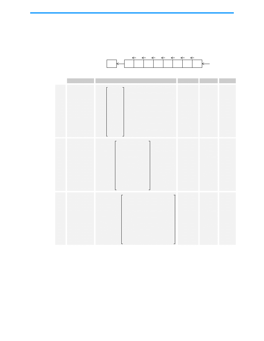
Section 4. M8C Instruction Set
August 12, 2004
Document #: 38-12004 Rev. *B
43
4.4
Arithmetic Shift Left
ASL
Description:
Shifts all bits of the instruction’s argument one bit to the left. Bit 7 is
loaded into the Carry Flag and bit 0 is loaded with a zero.
Arguments
Operation
Opcode
Cycles
Bytes
ASL
A
0x64
4
1
ASL
[expr]
0x65
7
2
ASL
[X+expr]
0x66
8
2
Conditional Flags:
CF
Set equal to the initial argument’s bit 7 value.
ZF
Set if the result is zero; cleared otherwise.
Example 1:
mov A, 0x7F
;initialize A with 127
asl A
;A=0xFE, CF=0, ZF=0
Example 2:
mov [0xEB], AA ;initialize RAM @ 0xEB with 0
asl [0xEB]
;ram[0xEB]=54, CF=1, ZF=0
7
4
5
2
3
0
1
CF
0
6
A
CF
A:7
←
A:7
A:6
←
A:6
A:5
←
A:5
A4
←
A:4
A:3
←
A:3
A:2
←
A:2
A:1
←
A:1
A:0
←
A:0
0
←
←
ram k
[ ]
CF
ram k
[ ]:7
←
ram k
[ ]:7
ram k
[ ]:6
←
ram k
[ ]:6
ram k
[ ]:5
←
ram k
[ ]:5
ram k
[ ]:4
←
ram k
[ ]:4
ram k
[ ]:3
←
ram k
[ ]:3
ram k
[ ]:2
←
ram k
[ ]:2
ram k
[ ]:1
←
ram k
[ ]:1
ram k
[ ]:0
←
ram k
[ ]:0
0
←
←
ram X k
+
[
]
CF
ram X k
+
(
)
[
]:7
←
ram X k
+
(
)
[
]:7
ram X k
+
(
)
[
]:6
←
ram X k
+
(
)
[
]:6
ram X k
+
(
)
[
]:5
←
ram X k
+
(
)
[
]:5
ram X k
+
(
)
[
]:4
←
ram X k
+
(
)
[
]:4
ram X k
+
(
)
[
]:3
←
ram X k
+
(
)
[
]:3
ram X k
+
(
)
[
]:2
←
ram X k
+
(
)
[
]:2
ram X k
+
(
)
[
]:1
←
ram X k
+
(
)
[
]:1
ram X k
+
(
)
[
]:0
←
ram X k
+
(
)
[
]:0
0
←
←
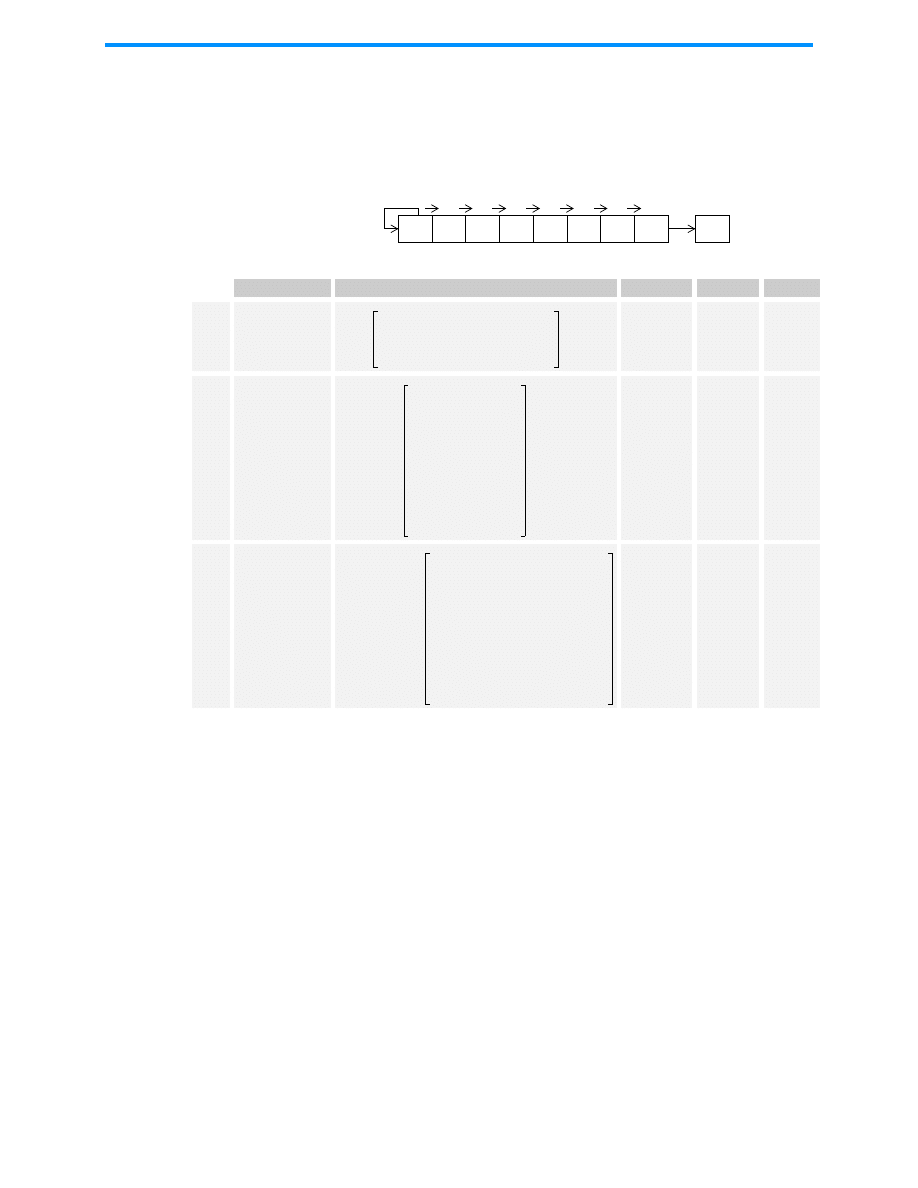
PSoC Designer: Assembly Language User Guide
44
Document #: 38-12004 Rev. *B
August 12, 2004
4.5
Arithmetic Shift Right
ASR
Description:
Shifts all bits of the instruction’s argument one bit to the right. Bit 7
remains the same while bit 0 is shifted into the Carry Flag.
Arguments
Operation
Opcode
Cycles
Bytes
ASR
A
0x67
4
1
ASR
[expr]
0x68
7
2
ASR
[X+expr]
0x69
8
2
Conditional Flags:
CF
Set if LSB of the source was set before the shift, else
cleared.
ZF
Set if the result is zero; cleared otherwise.
Example 1:
mov A, 0x00
;initialize A to 0
and F, 0x00
;make sure all flags are cleared
asr A
;A=0, CF=0, ZF=1
Example 2:
mov A, 0xFF
;initialize A to 255
and F, 0x00
;make sure all flags are cleared
asr A
;A=0xFF, CF=1, ZF=0
Example 3:
mov A, 0xAA
;initialize A to 170
and F, 0x00
;make sure all flags are cleared
asr A
;A=0xD5, CF=0, ZF=0
7
4
5
2
3
0
1
6
CF
A
CF
A:0, A:0
A:1, A:1
A:2
←
←
←
A:2
A:3, A:3
A:4, A:4
A:5
←
←
←
A:5
A:6, A:6
A:7
←
←
←
ram k
[ ]
CF
ram k
( )
[
]:0
←
ram k
[ ]:0
ram k
[ ]:1
←
ram k
[ ]:1
ram k
[ ]:2
←
ram k
[ ]:2
ram k
[ ]:3
←
ram k
[ ]:3
ram k
[ ]:4
←
ram k
[ ]:4
ram k
[ ]:5
←
ram k
[ ]:5
ram k
[ ]:6
←
ram k
[ ]:6
ram k
[ ]:7
←
←
ram X k
+
[
]
CF
ram X k
+
(
)
[
]:0
←
ram X k
+
(
)
[
]:0
ram X k
+
(
)
[
]:1
←
ram X k
+
(
)
[
]:1
ram X k
+
(
)
[
]:2
←
ram X k
+
(
)
[
]:2
ram X k
+
(
)
[
]:3
←
ram X k
+
(
)
[
]:3
ram X k
+
(
)
[
]:4
←
ram X k
+
(
)
[
]:4
ram X k
+
(
)
[
]:5
←
ram X k
+
(
)
[
]:5
ram X k
+
(
)
[
]:6
←
ram X k
+
(
)
[
]:6
ram X k
+
(
)
[
]:7
←
←

Section 4. M8C Instruction Set
August 12, 2004
Document #: 38-12004 Rev. *B
45
4.6
Call Function
CALL
Description:
Adds the signed argument to the current PC+2 value resulting in a
new PC that determines the address of the first byte of the next
instruction. The current PC value is defined as the PC value that
corresponds to the ROM address of the first byte of the next
instruction.
Two pushes are used to store the Program Counter (PC+2) on the
stack. First, the upper 8-bits of the PC are placed on the stack fol-
lowed by the lower 8-bits. The Stack Pointer is post-incremented
for each push. For devices with more than 256 bytes of RAM, the
stack is confined to a single designated stack page defined in the
device data sheet. The M8C automatically selects the stack page
as the destination for the push during the CALL instruction. There-
fore, a CALL instruction may be issued in any RAM page. After the
CALL has completed, user code will be operating from the same
RAM page as before the CALL instruction was executed.
This instruction has a 12-bit twos-complement relative address that
is added to the PC. The 12 bits are packed into the two-byte
instruction format by using the lower nibble of the opcode and the
second byte of the instruction format. Therefore, all opcodes with
an upper nibble of 9 are call instructions. The “x” character is
used in the table below to indicate that the first byte of a call
instruction can have one of 16 values (i.e., 0x90, 0x91,
0x92,...,0x9F).
Arguments
Operation
Opcode
Cycles
Bytes
CALL
expr
0x9x
11
2
Conditional Flags:
CF
Unaffected.
ZF
Unaffected.
Example:
0000
_main:
0000 40
nop
0001 90 E8 call SubFun
0003 40 nop
Note that the relative address for the CALL above is positive
(0xE8) and that the sum of that address and the PC value for the
first byte of the next instruction (0x0003) equals the address of the
SubFun label
(0xE8 + 0x0003 = 0x00EB)
0004
9F FA call _main
Note that the call to Main uses a negative address (0xFA).
0006
00EB
org 0x00EB
00EB
SubFun:
00EB
40
nop
00EC
7F ret
PC
PC 2 k
2048
–
k 2047
≤ ≤
(
)
,
+ +
←

PSoC Designer: Assembly Language User Guide
46
Document #: 38-12004 Rev. *B
August 12, 2004
4.7
Non-destructive Compare
CMP
4.8
Complement Accumulator
CPL
Description:
Subtracts the second argument from the first. If the difference is
less than zero the Carry Flag is set. If the difference is 0 the Zero
Flag is set. Neither operand’s value is destroyed by this instruction.
Arguments
Operation
Opcode
Cycles
Bytes
CMP
A, expr
0x39
5
2
CMP
A, [expr]
0x3A
7
2
CMP
A, [X+expr]
0x3B
8
2
CMP
[expr], expr
0x3C
8
3
CMP
[X+expr], expr
0x3D
9
3
Conditional Flags:
CF
Set if Operand 1 < Operand 2; cleared otherwise.
ZF
Set if the operands are equal; cleared otherwise.
Example:
mov A, 34
;initialize the accumulator to 34
cmp A, 33
;A>=34 CF cleared, A != 33 ZF cleared
cmp A, 34
;A=34 CF cleared, ZF set
cmp A, 35
;A<35 CF set, A != 35 ZF cleared
Description:
Computes the bitwise complement of the Accumulator and stores
the result in the Accumulator. The Carry Flag is not affected but the
Zero Flag will be set if the result of the complement is 0 (i.e., the
original value was 0xFF).
Arguments
Operation
Opcode
Cycles
Bytes
CPL
A
0x73
4
1
Conditional Flags:
CF
Unaffected.
ZF
Set if the result is zero; cleared otherwise.
Example 1:
mov A, 0xFF
cpl A
;A=0x00, ZF=1
Example 2:
mov A, 0xA5
cpl A
;A=0x5A, ZF=0
Example 3:
mov A, 0xFE
cpl A
;A=0x01, ZF=0
A k
–
A ram k
[ ]
–
A ram X k
+
[
]
–
ram k
1
[ ] k
2
–
ram X k
1
+
[
] k
2
–
A
A
←

Section 4. M8C Instruction Set
August 12, 2004
Document #: 38-12004 Rev. *B
47
4.9
Decrement
DEC
4.10
Halt
HALT
Description:
Subtracts one from the value of the argument and replaces the
argument’s original value with the result. If the result is -1 (original
value was zero) the Carry Flag is set. If the result is 0 (original
value was one) the Zero Flag is set.
Arguments
Operation
Opcode
Cycles
Bytes
DEC
A
0x78
4
1
DEC
X
0x79
4
1
DEC
[expr]
0x7A
7
2
DEC
[X+expr]
0x7B
8
2
Conditional Flags:
CF
Set if the result is -1; cleared otherwise.
ZF
Set if the result is zero; cleared otherwise.
Example:
mov [0xEB], 3
loop2:
;The loop will be executed 3 times.
dec [0xEB]
jnz loop2
;Jump will not be taken when ZF is
;set by DEC (i.e. wait until the
;loop counter (0xEB) is decremented
;to 0x00).
Description:
Halts the execution of the processor. The processor will remain
halted until a Power-On-Reset (POR), Watchdog Timer Reset
(WDR), or external reset (XRES) event occurs. The POR, WDR,
and XRES are all hardware resets which will cause a complete
system reset including the resetting of registers to their power-on
state. Watchdog reset will not cause the Watchdog Timer to be dis-
abled while all other resets will disable the Watchdog Timer.
Arguments
Operation
Opcode
Cycles
Bytes
HALT
0x30
9
1
Conditional Flags:
CF
Carry Flag unaffected.
ZF
Zero Flag unaffected.
Example:
halt
;sets STOP bit in CPU_SCR register
A
A 1
–
←
X
X 1
–
←
ram k
[ ]
ram k
[ ] 1
–
←
ram X k
+
[
]
ram X k
+
[
] 1
–
←
reg CPU_SCR
[
]
reg CPU_SCR
[
] 1
+
←

PSoC Designer: Assembly Language User Guide
48
Document #: 38-12004 Rev. *B
August 12, 2004
4.11
Increment
INC
Description:
Adds one to the argument. The argument’s original value is
replaced by the new value. If the value after the increment is 0x00
the Carry Flag and the Zero Flag will be set (original value must
have been 0xFF).
Arguments
Operation
Opcode
Cycles
Bytes
INC
A
0x74
4
1
INC
X
0x75
4
1
INC
[expr]
0x76
7
2
INC
[X+expr]
0x77
8
2
Conditional Flags:
CF
Set if value after the increment is 0; cleared otherwise.
ZF
Set if the result is zero; cleared otherwise.
Example 1:
mov A, 0x00
;initialize A to 0
or
F, 0x06
;make sure CF and ZF are set (1)
inc A
;A=0x01, CF=0, ZF=0
Example 2:
mov A, 0xFF
;initialize A to 0
and F, 0x00
;make sure flags are all 0
inc A
;A=0x00, CF=1, ZF=1
A
A 1
+
←
X
X 1
+
←
ram k
[ ]
ram k
[ ] 1
+
←
ram X k
+
[
]
ram X k
+
[
]
←

Section 4. M8C Instruction Set
August 12, 2004
Document #: 38-12004 Rev. *B
49
4.12
Relative Table Read
INDEX
Description:
Places the contents of ROM at the location indicated by the sum of
the Accumulator, the argument, and the current PC+2 into the
Accumulator. This instruction has a 12-bit, two’s-complement off-
set-address, relative to the current PC+2. The current PC value is
defined as the PC value that corresponds to the ROM address of
the first byte of the instruction.
The INDEX instruction is used to retrieve information from a table
to the Accumulator. The lower nibble of the first byte of the instruc-
tion is used as the upper 4 bits of the 12-bit address. Therefore, all
instructions that begin with 0xF are INDEX instructions, so all of
the following are INDEX “opcodes”: 0xF0, 0xF1,
0xF2,...,0xFF.
The offset into the table is taken as the value of the Accumulator
when the INDEX instruction is executed. The maximum readable
table size is 256 bytes due to the Accumulator being 8 bits in
lengths.
Arguments
Operation
Opcode
Cycles
Bytes
INDEX
expr
0xFx
13
2
Conditional Flags:
CF
Unaffected.
ZF
Set if the byte returned to A is zero.
Example:
0000
OUT_REG: equ 04h
0000
40
[04]
nop
0001
50 03
[04]
mov A, 3
0003
F0 E6
[13]
index ASCIInumbers
0005
60 04
[05]
mov reg[OUT_REG], A
Note that the 12-bit address for the INDEX instruction is positive
and that the sum of the address (0x0E6) and the next instruction’s
address (0x0005) are equal to the first address of the ASCIInum-
bers table (0x00EB). Because the accumulator has been set to 3
before executing the INDEX instruction the fourth byte in the ASCI-
Inumbers table will be returned to A. Therefore, A will be 0x33 at
the end of the INDEX instruction.
0007
00EB
org 0x00EB
00EB
ASCIInumbers:
00EB
30 31 ... ds "0123456789"
32 33 34 35 36 37 38 39
A
rom k A PC 2
+ +
+
[
], 2048 k
≤
–
2047
≤
(
)
←

PSoC Designer: Assembly Language User Guide
50
Document #: 38-12004 Rev. *B
August 12, 2004
4.13
Jump Accumulator
JACC
Description:
Jump, unconditionally, to the address computed by the sum of the
Accumulator, the 12-bit twos-compliment argument, and the cur-
rent PC+1. The current PC value is defined as the PC value that cor-
responds to the ROM address of the first byte of the JACC
instruction.
The Accumulator is not affected by this instruction. The JACC
instruction uses a two-byte instruction format where the lower nib-
ble of the first byte is used for the upper 4 bits of the 12-bit relative
address. This causes an effective 4-bit opcode. Therefore, the fol-
lowing are all valid “opcode” bytes for the JACC instruction: 0xE0,
0xE1, 0xE2,...,0xEF.
Arguments
Operation
Opcode
Cycles
Bytes
JACC
expr
0xEx
7
2
Conditional Flags:
CF
Unaffected.
ZF
Unaffected.
Example:
0000 _main:
0000
50 03
mov A, 3 ;set A with jump offset
0002
E0 01
jacc
SubFun
Program execution will jump to address 0x0007 (halt)
0004
SubFun:
0004
40
nop
0005
40
nop
0006
40
nop
0007
30
halt
PC
PC 1
+
(
) k A
+ +
←

Section 4. M8C Instruction Set
August 12, 2004
Document #: 38-12004 Rev. *B
51
4.14
Jump if Carry
JC
Description:
If the Carry Flag is set, jump to the sum of the relative address
argument and the current PC+1. The current PC value is defined as
the PC value that corresponds to the ROM address of the first byte
of the JC instruction.
The JC instruction uses a two-byte instruction format where the
lower nibble of the first byte is used for the upper 4 bits of the 12-bit
relative address. This causes an effective 4-bit opcode. Therefore,
the following are all valid “opcode” bytes for the JC instruction:
0xC0, 0xC1, 0xC2,...,0xCF.
Arguments
Operation
Opcode
Cycles
Bytes
JC
expr
0xCx
5
2
Conditional Flags:
CF
Carry Flag unaffected.
ZF
Zero Flag unaffected.
Example:
0000 _main:
0000
55 3C 02 mov [3Ch], 2
0003
16 3C 03 sub [3Ch], 3 ;2-2=0 CF=1, ZF=0
0006
C0 02
jc SubFun ;CF=1, jump to SubFun
0008
30
halt
0009
0009 SubFun:
0009
40
nop
PC
PC 1
+
(
) k
+
←
, 2048
–
k 2047
≤ ≤
(
)

PSoC Designer: Assembly Language User Guide
52
Document #: 38-12004 Rev. *B
August 12, 2004
4.15
Jump
JMP
Description:
Jump unconditionally to the address indicated by the sum of the
argument and the current PC+1. The current PC value is defined as
the PC value that corresponds to the ROM address of the first byte
of the JMP instruction.
The JMP instruction uses a two-byte instruction format where the
lower nibble of the first byte is used for the upper 4 bits of the 12-bit
relative address. This causes an effective 4-bit opcode. Therefore,
the following are all valid “opcode” bytes for the JMP instruction:
0x80, 0x81, 0x82,...,0x8F.
Arguments
Operation
Opcode
Cycles
Bytes
JMP
expr
0x8x
5
2
Conditional Flags:
CF
Carry Flag unaffected.
ZF
Zero Flag unaffected.
Example:
0000
_main:
0000
80 01
[05]
jmp SubFun
Jump is forward, relative to PC, therefore offset is positive (0x01).
0002
SubFun:
0002
8F FD
[05]
jmp _main
Jump is backwards, relative to PC, therefore, offset is negative
(0xFD).
PC
PC 1
+
(
) k
+
←
, 2048
–
k 2047
≤ ≤
(
)

Section 4. M8C Instruction Set
August 12, 2004
Document #: 38-12004 Rev. *B
53
4.16
Jump if No Carry
JNC
Description:
If the Carry Flag is not set, jump to the sum of the relative address
argument and the current PC+1. The current PC value is defined as
the PC value that corresponds to the ROM address of the first byte
of the JNC instruction.
The JNC instruction uses a two-byte instruction format where the
lower nibble of the first byte is used for the upper 4 bits of the 12-bit
relative address. This causes an effective 4-bit opcode. Therefore,
the following are all valid “opcode” bytes for the JNC instruction:
0xD0, 0xD1, 0xD2,...,0xDF.
Arguments
Operation
Opcode
Cycles
Bytes
JNC
expr
0xDx
5
2
CF
Carry Flag unaffected.
ZF
Zero Flag unaffected.
Example:
0000 _main:
0000
55 3C 02 [08]
mov [3Ch], 2
0003
16 3C 02 [09]
sub [3Ch], 2 ;2-2=0 CF=0, ZF=1
0006
D0 02
[05]
jnc SubFun ; jump to SubFun
0008
30
[04]
halt
0009
0009 SubFun:
0009
40
[04]
nop
PC
PC 1
+
(
) k
+
←
, 2048
–
k 2047
≤ ≤
(
)

PSoC Designer: Assembly Language User Guide
54
Document #: 38-12004 Rev. *B
August 12, 2004
4.17
Jump if Not Zero
JNZ
Description:
If the Zero Flag is not set, jump to the address indicated by the sum
of the argument and the current PC+1. The current PC value is
defined as the PC value that corresponds to the ROM address of
the first byte of the JNZ instruction.
The JNZ instruction uses a two-byte instruction format where the
lower nibble of the first byte is used for the upper 4 bits of the 12-bit
relative address. This causes an effective 4-bit opcode. Therefore,
the following are all valid “opcode” bytes for the JNZ instruction:
0xB0, 0xB1, 0xB2,...,0xBF.
Arguments
Operation
Opcode
Cycles
Bytes
JNZ
expr
0xBx
5
2
Conditional Flags:
CF
Carry Flag unaffected.
ZF
Zero Flag unaffected.
Example:
0000 _main:
0000
55 3C 02 [08]
mov [3Ch], 2
0003
16 3C 01 [09]
sub [3Ch], 1 ;2-1=1 CF=0, ZF=0
0006
B0 02
[05]
jnz SubFun ;jump to SubFun
0008
30
[04]
halt
0009
0009 SubFun:
0009
40
[04]
nop
PC
PC 1
+
(
) k
+
←
, 2048
–
k 2047
≤ ≤
(
)

Section 4. M8C Instruction Set
August 12, 2004
Document #: 38-12004 Rev. *B
55
4.18
Jump if Zero
JZ
Description:
If the Zero Flag is set, jump to the address indicated by the sum of
the argument and the current PC+1. The current PC value is
defined as the PC value that corresponds to the ROM address of
the first byte of the JZ instruction.
The JZ instruction uses a two-byte instruction format where the
lower nibble of the first byte is used for the upper 4 bits of the 12-bit
relative address. This causes an effective 4-bit opcode. Therefore,
the following are all valid “opcode” bytes for the JZ instruction:
0xA0, 0xA1, 0xA2,...,0xAF.
Arguments
Operation
Opcode
Cycles
Bytes
JZ
expr
0xAx
5
2
Conditional Flags:
CF
Carry Flag unaffected.
ZF
Zero Flag unaffected.
Example:
0000
_main:
0000
55 3C 02 [08]
mov [3Ch], 2
0003
16 3C 02 [09]
sub [3Ch], 2 ;2-2=0 CF=0, ZF=1
0006
A0 02
[05]
jz SubFun ;jump to SubFun
0008
30
[04]
halt
0009
0009
SubFun:
0009
40
[04]
nop
PC
PC 1
+
(
) k
+
←
, 2048
–
k 2047
≤ ≤
(
)

PSoC Designer: Assembly Language User Guide
56
Document #: 38-12004 Rev. *B
August 12, 2004
4.19
Long Call
LCALL
Description:
Replaces the PC value with the LCALL instruction’s argument. The
new PC value determines the address of the first byte of the next
instruction.
Two pushes are used to store the Program Counter (current PC+3)
on the stack. The current PC value is defined as the PC value that
corresponds to the ROM address of the first byte of the instruction.
First, the upper 8 bits of the PC+3 are placed on the stack followed
by the lower 8 bits. The Stack Pointer is post-incremented for each
push. For PSoC microcontrollers with more than 256 bytes of
RAM, the stack is confined to a single designated stack page
defined in the device data sheet. The M8C automatically selects
the stack page as the destination for the push during the LCALL
instruction. Therefore, a LCALL instruction may be issued in any
RAM page. After the LCALL has completed, user code will be oper-
ating from the same RAM page as before the LCALL instruction
was executed.
This instruction has a 16-bit unsigned address. A three-byte
instruction format is used where the first byte is a full 8-bit opcode.
Arguments
Operation
Opcode
Cycles
Bytes
LCALL
expr
0x7C
13
3
Conditional Flags:
CF
Unaffected.
ZF
Unaffected.
Example:
0000
_main:
0000
7C 00 05 [13]
lcall SubFun
0003
8F FC
[05]
jmp _main
Although in this example a full 16-bit address is not needed for the
call to SubFun the listing above shows that the lcall instruction
is using a three byte format which accommodates the 16-bit abso-
lute jump address of 0x0005.
0005
0005 SubFun:
0005
7F
[08]
ret
ram SP
[
]
PC 3
+
(
) 15:8
[
]
SP
SP 1
ram SP
[
]
PC 3
+
(
) 7:0
[
]
SP
SP 1
PC
k, 0 k 65535
≤ ≤
(
)
←
+
←
←
+
←
←

Section 4. M8C Instruction Set
August 12, 2004
Document #: 38-12004 Rev. *B
57
4.20
Long Jump
LJMP
Description:
Jump unconditionally to the unsigned address indicated by the
instruction’s argument. The LJMP instruction uses a three-byte
instruction format to accommodate a full 16-bit argument. The first
byte of the instruction is a full 8-bit opcode.
Arguments
Operation
Opcode
Cycles
Bytes
LJMP
expr
0x7D
7
3
Conditional Flags:
CF
Unaffected.
ZF
Unaffected.
Example:
0000
_main:
0000
7D 00 03 [07]ljmp SubFun
Although in this example a full 16-bit address is not needed for the
jump to SubFun the listing above shows that the ljmp instruction
is using a three byte format which accommodates the 16-bit abso-
lute jump address of 0x0003.
0003
0003 SubFun:
0003
7D 00 00 [07]ljmp _main
Note that this instruction is jumping backwards, relative to the cur-
rent PC value, and the address in the instruction is a positive num-
ber (0x0000). This is because the ljmp instruction uses an
absolute address.
PC
K, 0 k 65535
≤ ≤
(
)
←
PSoC Designer: Assembly Language User Guide
58
Document #: 38-12004 Rev. *B
August 12, 2004
4.21
Move
MOV
Description:
This instruction allows for a number of combinations of moves.
Immediate, direct, and indexed addressing are supported.
Arguments
Operation
Opcode
Cycles
Bytes
MOV
X, SP
0x4F
4
1
MOV
A, expr
0x50
4
2
MOV
A, [expr]
0x51
5
2
MOV
A, [X+expr]
0x52
6
2
MOV
[expr], A
0x53
5
2
MOV
[X+expr], A
0x54
6
2
MOV
[expr], expr
0x55
8
3
MOV
[X+expr], expr
0x56
9
3
MOV
X, expr
0x57
4
2
MOV
X, [expr]
0x58
6
2
MOV
X, [X+expr]
0x59
7
2
MOV
[expr], X
0x5A
5
2
MOV
A, X
0x5B
4
1
MOV
X, A
0x5C
4
1
MOV
A, reg[expr]
0x5D
6
2
MOV
A, reg[X+expr]
0x5E
7
2
MOV
[expr], [expr]
0x5F
10
3
MOV
REG[expr], A
0x60
5
2
MOV
REG[X+expr], A
0x61
6
2
MOV
REG[expr], expr
0x62
8
3
MOV
REG[X+expr], expr
0x63
9
3
Condition Flags:
CF
Carry Flag unaffected.
ZF
Set if A is the destination and the result is zero.
Example:
mov A, 0x01
;accumulator will equal 1, ZF=0
mov A, 0x00
;accumulator will equal 0, ZF=1
X
SP
←
A
k
←
A
ram k
[ ]
←
A
ram X k
+
[
]
←
ram k
[ ]
A
←
ram X k
+
[
]
A
←
ram k
1
[ ]
k
2
←
ram X k
1
+
[
]
k
2
←
X
k
←
X
ram k
[ ]
←
X
ram X k
+
[
]
←
ram k
[ ]
X
←
A
X
←
X
A
←
A
reg k
[ ]
←
A
reg X k
+
[
]
←
ram k
1
[ ]
ram k
2
[ ]
←
reg k
[ ]
A
←
reg X k
+
[
]
A
←
reg k
1
[ ]
k
2
←
reg X k
1
+
[
]
k
2
←

Section 4. M8C Instruction Set
August 12, 2004
Document #: 38-12004 Rev. *B
59
4.22
Move Indirect, Post-Increment to Memory
MVI
Description:
A data pointer in RAM is used to move data between another RAM
address and the Accumulator. The data pointer is incremented
after the data transfer has completed.
For PSoC microcontrollers with more than 256 bytes of RAM, spe-
cial page pointers are used to allow the MVI instructions to access
data in remote RAM pages. Two page pointers are available, one
for MVI read (MVI A,
[
[expr]++]) and another for MVI write
(MVI [[expr]++], A). The data pointer is always found in the
current RAM page. The page pointers determine which RAM page
the data pointer’s address will be used. At the end of an MVI
instruction, user code will be operating from the same RAM page
as before the MVI instruction was executed.
Arguments
Operation
Opcode
Cycles
Bytes
MVI
A, [[expr]++]
0x3E
10
2
MVI
[[expr]++], A
0x3F
10
2
Conditional Flags:
CF
Unaffected.
ZF
Set if A is updated with zero.
A
ram ram k
[ ]
[
]
ram k
[ ]
ram k
[ ] 1
+
←
←
ram ram k
[ ]
[
]
A
ram k
[ ]
ram k
[ ] 1
+
←
←

PSoC Designer: Assembly Language User Guide
60
Document #: 38-12004 Rev. *B
August 12, 2004
4.23
No Operation
NOP
Example 1:
mov [10h], 4
mov [11h], 3
mov [EBh], 10h ;initialize MVI read pointer to 10h
mvi A, [EBh]
;A=4, ram[EBh]=11h
mvi A, [EBh]
;A=3, ram[EBh]=12h
Example 2:
mov [EBh], 10h ;initialize MVI write pointer to 10h
mov A, 8
mvi [EBh], A
;ram[10h]=8, ram[EBh]=11h
mov A, 1
mvi [EBh], A
;ram[11h]=1, ram[EBh]=12h
Multi-Page Example 3:
mov reg[CUR_PP], 2;set Current Page Pointer to 2
mov [10h], 4
;ram_2[10h]=4
mov [11h], 3
;ram_2[11h]=3
mov reg[CUR_PP], 0;set Current Page Pointer back to 0
mov reg[MVW_PP], 2;set MVI write RAM page pointer
mov [EBh], 10h ;initialize MVI read pointer to 10h
mvi A, [EBh]
;A=4, ram_0[EBh]=11h
mvi A, [EBh]
;A=3, ram_0[EBh]=12h
Multi-Page Example 4:
mov reg[CUR_PP], 0;set Current Page Pointer to 0
mov reg[MVR_PP], 3;set MVI read RAM page pointer
mov [EBh], 10h ;initialize MVI write pointer to 10h
mov A, 8
mvi [EBh], A
;ram_3[10h]=8, ram_0[EBh]=11h
mov A, 1
mvi [EBh], A
;ram_3[11h]=1, ram_0[EBh]=12h
Description:
This one-byte instruction performs no operation, but, consumes 4
CPU clock cycles.
Arguments
Operation
Opcode
Cycles
Bytes
NOP
None
0x40
4
1
Conditional Flags:
CF
Carry Flag unaffected.
ZF
Zero Flag unaffected.
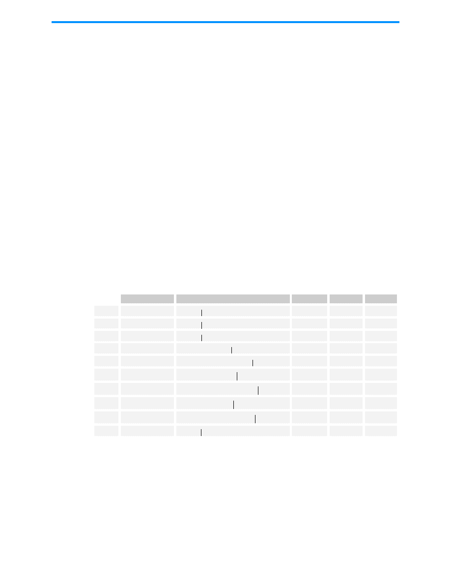
Section 4. M8C Instruction Set
August 12, 2004
Document #: 38-12004 Rev. *B
61
4.24
Bitwise OR
OR
Description:
Computes the logical OR for each bit position using both argu-
ments. The result of the logical OR is placed in the corresponding
bit position for the first argument.
The Carry Flag is only changed when the OR F, expr instruction
is used. The Carry Flag will be set to the result of the logical OR of
the Carry Flag at the beginning of instruction execution and the
second argument’s value at bit position 2 (i.e., F[2] and
expr[2]).
For the OR F, expr instruction the Zero Flag is handled the same
as the Carry Flag in that it is changed as a result of the logical OR
of the Zero Flag’s value at the beginning of instruction execution
and the value of the second arguments value at bit position 1 (i.e.,
F[1] and expr[1]). However, for all other OR instructions the
Zero Flag will be set or cleared based on the result of the logical
OR operation. If the result of the OR is that all bits are zero, the
Zero Flag will be set, otherwise the Zero Flag is cleared.
Note that OR (or AND or XOR, as appropriate) is a read-modify
write instruction. When operating on a register, that register must
be of the read-write type. Bitwise OR to a write-only register will
generate nonsense.
Arguments
Operation
Opcode
Cycles
Bytes
OR
A, expr
0x29
4
2
OR
A, [expr]
0x2A
6
2
OR
A, [X+expr]
0x2B
7
2
OR
[expr], A
0x2C
7
2
OR
[X+expr], A
0x2D
8
2
OR
[expr], expr
0x2E
9
3
OR
[X+expr], expr
0x2F
10
3
OR
REG[expr], expr
0x43
9
3
OR
REG[X+expr], expr
0x44
10
3
OR
F, expr
0x71
4
2
A
A k
←
A
A ram k
[ ]
←
A
A ram X k
+
[
]
←
ram k
[ ]
ram k
[ ] A
←
ram X k
+
[
]
ram X k
+
[
] A
←
ram k
1
[ ]
ram k
1
[ ] k
2
←
ram X k
1
+
[
]
ram X k
1
+
[
] k
2
←
reg k
1
[ ]
reg k
1
[ ] k
2
←
reg X k
1
+
[
]
reg X k
1
+
[
] k
2
←
F
F k
←

PSoC Designer: Assembly Language User Guide
62
Document #: 38-12004 Rev. *B
August 12, 2004
4.25
Pop Stack into Register
POP
Conditional Flags:
CF
Unaffected (unless F is destination).
ZF
Set if the result is zero; cleared otherwise (unless F is desti-
nation).
Example 1:
mov A, 0x00
or
A, 0xAA
;A=0xAA, CF=unchanged, ZF=0
Example 2:
and F, 0x00
or
F, 0x01
;F=1 therefore CF=0, ZF=0
Description:
Remove the last byte placed on the stack and put it in the specified
M8C register. The Stack Pointer is automatically decremented. The
Zero Flag is set if the popped value is zero, otherwise the Zero
Flag is cleared. The Carry Flag is not affected by this instruction.
For PSoC devices with more than 256 bytes of RAM, the stack is
confined to a single designated stack page defined by the value of
the STK_PP Register. The M8C automatically selects the stack
page as the source for the memory read during the POP instruction.
Therefore, a POP instruction may be issued in any RAM page. After
the POP has completed, user code will be operating from the same
RAM page as before the POP instruction was executed.
See the RAM Paging chapter of the PSoC Technical Reference
Manual (TRM) for details.
Arguments
Operation
Opcode
Cycles
Bytes
POP
A
0x18
5
1
POP
X
0x20
5
1
Conditional Flags:
CF
Carry Flag unaffected.
ZF
Set if A is updated to zero.
Example 1:
mov A, 34
push A
;top value of stack is now 34, SP+1
mov A, 0
;clear the Accumulator
pop A
;A=34, SP-1
Example 2:
mov A, 34
push A
;top value of stack is now 34, SP+1
pop X
;X=34, SP-1
A
ram SP 1
–
[
]
SP
SP 1
–
←
←
X
ram SP 1
–
[
]
SP
SP 1
–
←
←

Section 4. M8C Instruction Set
August 12, 2004
Document #: 38-12004 Rev. *B
63
4.26
Push Register onto Stack
PUSH
Description:
Transfer the value from the specified M8C register to the top of the
stack as indicated by the value of the SP at the start of the instruc-
tion. After placing the value on the stack, the SP is incremented.
The Zero Flag is set if the pushed value is zero, else the Zero Flag
is cleared. The Carry Flag is not affected by this instruction.
For PSoC microcontrollers with more than 256 bytes of RAM, the
stack is confined to a single designated stack page defined by the
value of the STK_PP Register. The M8C automatically selects the
stack page as the source for the memory write during the PUSH
instruction. Therefore, a PUSH instruction may be issued in any
PUSH page. After the PUSH has completed user code will be oper-
ating from the same RAM page as before the PUSH instruction
was executed.
See the RAM Paging chapter of the PSoC Technical Reference
Manual (TRM) for details.
Arguments
Operation
Opcode
Cycles
Bytes
PUSH
A
0x08
4
1
PUSH
X
0x10
4
1
Conditional Flags:
CF
Carry Flag unaffected.
ZF
Zero Flag unaffected.
Example 1:
mov A, 0x3E
push A
;top value of stack is now 0x3E, SP+1
Example 2:
mov X, 0x3F
push X
;top value of stack is now 0x3F, SP+1
ram SP
[
]
A
←
SP
SP 1
+
←
ram SP
[
]
X
←
SP
SP 1
+
←

PSoC Designer: Assembly Language User Guide
64
Document #: 38-12004 Rev. *B
August 12, 2004
4.27
Return
RET
Description:
The last two bytes placed on the stack are used to change the PC.
The lower 8 bits of the PC are popped off the stack first followed by
the SP being decremented by one. Next the upper 8 bits of the PC
are popped off the stack followed by a decrement of the SP. Neither
Carry or Zero Flag is affected by this instruction.
For PSoC devices with more than 256 bytes of RAM, the stack is
confined to a single designated stack page defined by the value of
the STK_PP Register. The M8C automatically selects the stack
page as the source for the pop during the RET instruction. There-
fore, an RET instruction may be issued in any RAM page. After the
RET has completed, user code will be operating from the same
RAM page as before the RET instruction was executed.
See the RAM Paging chapter of the PSoC Technical Reference
Manual (TRM) for details.
Arguments
Operation
Opcode
Cycles
Bytes
RET
0x7F
8
1
Conditional Flags:
CF
Unaffected by this instruction.
ZF
Unaffected by this instruction.
Example:
0000
_main:
0000
90 02
[11]
call SubFun
0002
40
[04]
nop
0003
30
[04]
halt
0004
0004
SubFun:
0004
40
[04]
nop
0005
7F
[08]
ret
The ret instruction will set the PC to 0x0002, which is the starting
address of the first instruction after the call.
SP
SP 1
PC 7:0
[
]
ram SP
[
]
←
SP
SP 1
PC 15:8
[
]
ram SP
[
]
←
–
←
–
←

Section 4. M8C Instruction Set
August 12, 2004
Document #: 38-12004 Rev. *B
65
4.28
Return from Interrupt
RETI
Description:
The last three bytes placed on the stack are used to change the F
register and the PC. The first byte removed from the stack is used
to restore the F register. The SP is decremented after the first byte
is removed. The lower 8 bits of the PC are popped off the stack
next followed by the SP being decremented by one again. Finally
the upper 8 bits of the PC are popped off the stack followed by a
last decrement of the SP. The Carry and Zero Flags are updated
with the values from the first byte popped off the stack.
For PSoC devices with more than 256 bytes of RAM, the stack is
confined to a single designated stack page defined by the value of
the STK_PP Register. The M8C automatically selects the stack
page as the source for the pop during the RETI instruction. There-
fore, an RETI instruction may be issued in any RAM page. After
the RETI has completed, user code will be operating from the
same RAM page as before the RETI instruction was executed.
See the RAM Paging chapter of the PSoC Technical Reference
Manual (TRM) for details.
Arguments
Operation
Opcode
Cycles
Bytes
RETI
0x7E
10
1
Conditional Flags:
CF
All Flag bits are restored to the value pushed during an
interrupt call.
ZF
All Flag bits are restored to the value pushed during an
interrupt call.
Example:
SP
SP 1
F
ram SP
[
]
SP
SP 1
PC 7:0
[
]
ram SP
[
]
SP
SP 1
PC 15:8
[
]
ram SP
[
]
←
–
←
←
–
←
←
–
←
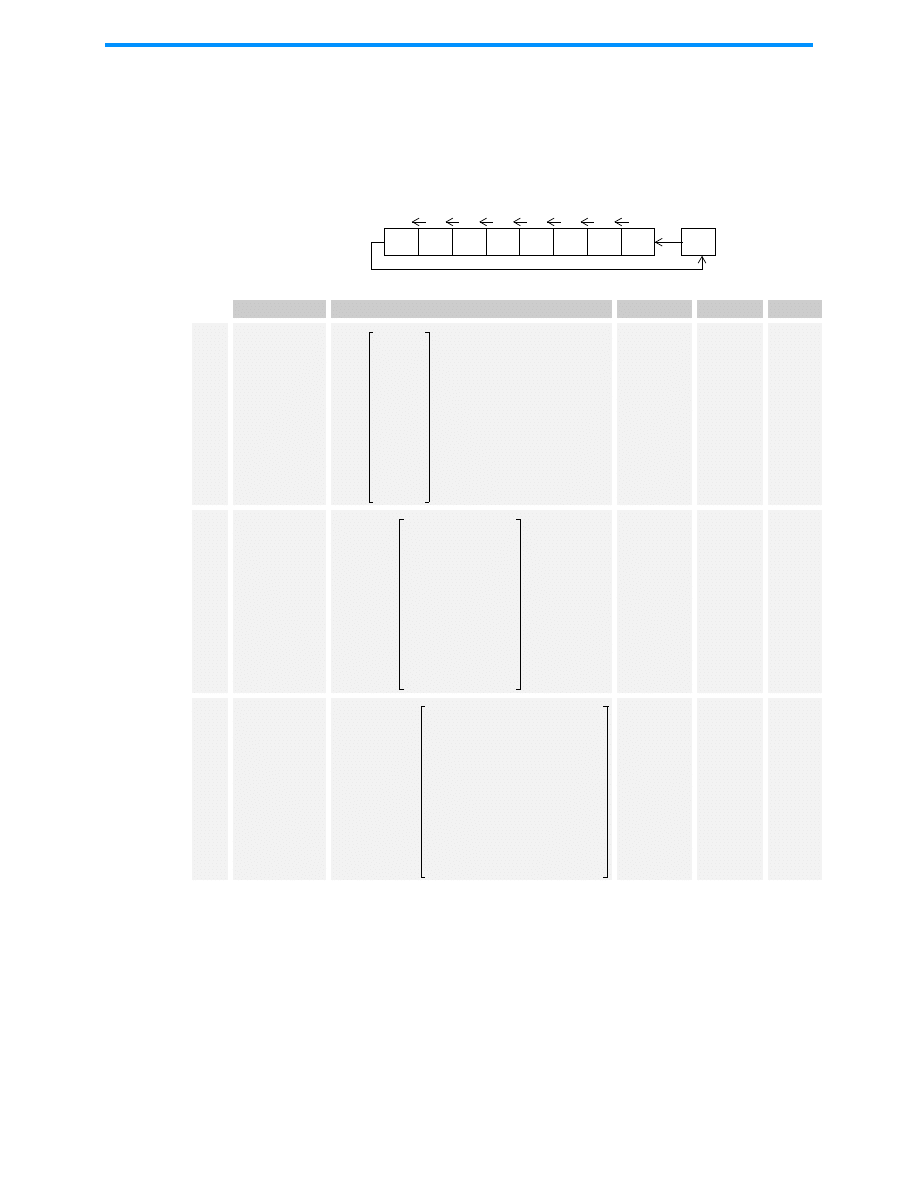
PSoC Designer: Assembly Language User Guide
66
Document #: 38-12004 Rev. *B
August 12, 2004
4.29
Rotate Left through Carry
RLC
Description:
Shifts all bits of the instruction’s argument one bit to the left. Bit 0 is
loaded with the Carry Flag. The most significant bit of the specified
location is loaded into the Carry Flag.
Arguments
Operation
Opcode
Cycles
Bytes
RLC
A
0x6A
4
1
RLC
[expr]
0x6B
7
2
RLC
[X+expr]
0x6C
8
2
Conditional Flags:
CF
Set if the MSB of the specified operand was set before the
shift, otherwise cleared.
ZF
Set if the result is zero; cleared otherwise.
Example 1:
and F, 0xFB
;clear carry flag
mov A, 0x7F
;initialize A with 127
rlc A
;A=0xFE, CF=0, ZF=0
7
4
5
2
3
0
1
6
CF
A
CF
A:7
←
A:7
A:6
←
A:6
A:5
←
A:5
A4
←
A:4
A:3
←
A:3
A:2
←
A:2
A:1
←
A:1
A:0
←
A:0
CF
←
←
ram k
[ ]
CF
ram k
[ ]:7
←
ram k
[ ]:7
ram k
[ ]:6
←
ram k
[ ]:6
ram k
[ ]:5
←
ram k
[ ]:5
ram k
[ ]:4
←
ram k
[ ]:4
ram k
[ ]:3
←
ram k
[ ]:3
ram k
[ ]:2
←
ram k
[ ]:2
ram k
[ ]:1
←
ram k
[ ]:1
ram k
[ ]:0
←
ram k 0
[ ]
[
]
CF
←
←
ram X k
+
[
]
CF
ram X k
+
(
)
[
]:7
←
ram X k
+
(
)
[
]:7
ram X k
+
(
)
[
]:6
←
ram X k
+
(
)
[
]:6
ram X k
+
(
)
[
]:5
←
ram X k
+
(
)
[
]:5
ram X k
+
(
)
[
]:4
←
ram X k
+
(
)
[
]:4
ram X k
+
(
)
[
]:3
←
ram X k
+
(
)
[
]:3
ram X k
+
(
)
[
]:2
←
ram X k
+
(
)
[
]:2
ram X k
+
(
)
[
]:1
←
ram X k
+
(
)
[
]:1
ram X k
+
(
)
[
]:0
←
ram X k
+
(
)
[
]:0
CF
←
←

Section 4. M8C Instruction Set
August 12, 2004
Document #: 38-12004 Rev. *B
67
4.30
Absolute Table Read
ROMX
Description:
Moves any byte from ROM (Flash) into the Accumulator. The
address of the byte to be retrieved is determined by the 16-bit
value formed by the concatenation of the A and X registers. The A
register is the most significant byte and the X register is the least
significant byte of the address. The Zero Flag is set if the retrieved
byte is zero, otherwise the Zero Flag is cleared. The Carry Flag is
not affected by this instruction.
Arguments
Operation
Opcode
Cycles
Bytes
ROMX
0x28
11
1
Conditional Flags:
CF
Unaffected.
ZF
Set if A is zero, cleared otherwise.
Example:
0000 _main:
0000
50 00
[04]
mov A, 00h
0002
57 08
[04]
mov X, 08h
0004
28
[11]
romx
0005
60 00
[05]
mov reg[00h], A
0007
40
[04]
nop
0008
30
[04]
halt
The romx instruction will read a byte from Flash at address
0x0008. The halt opcode is at address 0x0008, therefore, reg-
ister 0x00 will receive the value 0x30.
t1
PC 7:0
[
]
PC 7:0
[
]
X
t2
PC 15:8
[
]
PC 15:8
[
]
A
A
rom PC
[
]
PC 7:0
[
]
t1
PC 15:8
[
]
t2
←
←
←
←
←
←
←
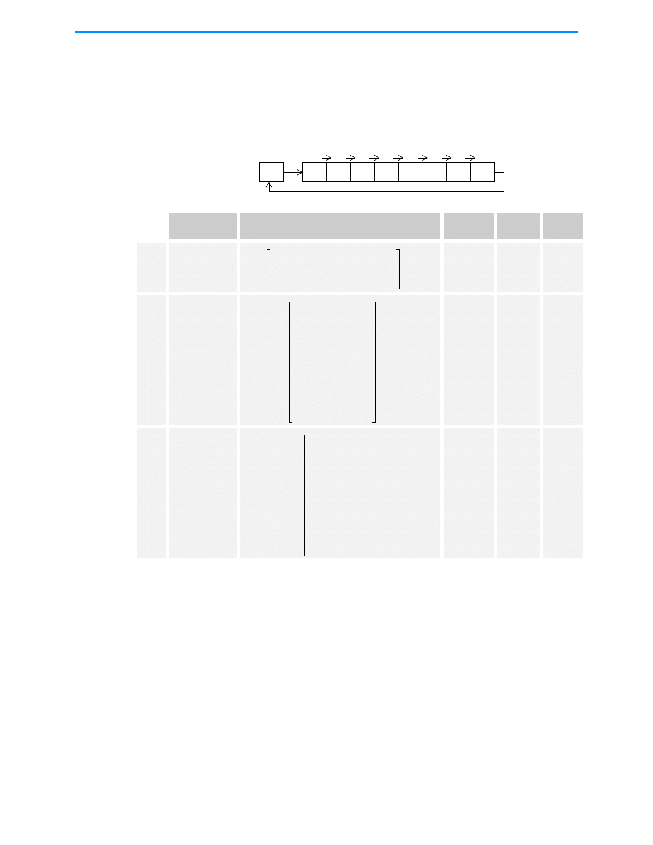
PSoC Designer: Assembly Language User Guide
68
Document #: 38-12004 Rev. *B
August 12, 2004
4.31
Rotate Right through Carry
RRC
Description:
Shifts all bits of the instruction’s argument one bit to the right. The
Carry Flag is loaded into the most significant bit of the argument.
Bit 0 of the argument is loaded into the Carry Flag.
Arguments
Operation
Opcode
Cycle
s
Bytes
RRC
A
0x6D
4
1
RRC
[expr]
0x6E
7
2
RRC
[X+expr]
0x6F
8
2
7
4
5
2
3
0
1
6
CF
A
CF
A:0, A:0
A:1, A:1
A:2
←
←
←
A:2
A:3, A:3
A:4, A:4
A:5
←
←
←
A:5
A:6, A:6
A:7, A:7
CF
←
←
←
←
ram k
[ ]
CF
ram k
( )
[
]:0
←
ram k
[ ]:0
ram k
[ ]:1
←
ram k
[ ]:1
ram k
[ ]:2
←
ram k
[ ]:2
ram k
[ ]:3
←
ram k
[ ]:3
ram k
[ ]:4
←
ram k
[ ]:4
ram k
[ ]:5
←
ram k
[ ]:5
ram k
[ ]:6
←
ram k
[ ]:6
ram k
[ ]:7
←
ram k
[ ]:7
CF
←
←
ram X k
+
[
]
CF
ram X k
+
(
)
[
]:0
←
ram X k
+
(
)
[
]:0
ram X k
+
(
)
[
]:1
←
ram X k
+
(
)
[
]:1
ram X k
+
(
)
[
]:2
←
ram X k
+
(
)
[
]:2
ram X k
+
(
)
[
]:3
←
ram X k
+
(
)
[
]:3
ram X k
+
(
)
[
]:4
←
ram X k
+
(
)
[
]:4
ram X k
+
(
)
[
]:5
←
ram X k
+
(
)
[
]:5
ram X k
+
(
)
[
]:6
←
ram X k
+
(
)
[
]:6
ram X k
+
(
)
[
]:7
←
ram X k
+
(
)
[
]:7
CF
←
←

Section 4. M8C Instruction Set
August 12, 2004
Document #: 38-12004 Rev. *B
69
4.32
Subtract with Borrow
SBB
Conditional Flags:
CF
Set if LSB of the specified operand was set before the shift,
cleared otherwise.
ZF
Set if the result is zero, cleared otherwise.
Example 1:
or
F, 0x04
;set carry flag
and A, 0x00
;clear the accumulator
rrc A
;A=0x80, CF=0, ZF=0
Example 2:
and F, 0xFB
;clear carry flag
mov A, 0xFF
;initialize A to 255
and A, 0x00
;make sure all flags are cleared
rrc A
;A=0x7F, CF=1, ZF=0
Example3:
or
F, 0x04
;set carry flag
mov [0xEB], 0xAA;initialize A to 170
rrc [0xEB]
;ram[0xEB]=0xD5, CF=1, ZF=0
Description:
Computes the difference of the two operands plus the carry value
from the Flag register. The first operand’s value is replaced by the
computed difference. If the difference is less than 0 the Carry Flag
is set in the Flag register. If the difference is zero, the Zero Flag is
set in the Flag register, otherwise the Zero Flag is cleared.
Arguments
Operation
Opcode
Cycles
Bytes
SBB
A, expr
0x19
4
2
SBB
A, [expr]
0x1A
6
2
SBB
A, [X+expr]
0x1B
7
2
SBB
[expr], A
0x1C
7
2
SBB
[X+expr], A
0x1D
8
2
SBB
[expr], expr
0x1E
9
3
SBB
[X+expr], expr
0x1F
10
3
Conditional Flags:
CF
Set if, treating the numbers as unsigned, the difference < 0;
cleared otherwise.
ZF
Set if the result is zero; cleared otherwise.
Example 1:
mov A, 0
;set accumulator to zero
or
F, 0x02
;set carry flag
sbb A, 12
;accumulator value is now 0xF3
Example 2:
mov [0x39], 2
;initialize ram[0x39]=0x02
mov [0x40], FFh ;initialize ram[0x40]=0xff
inc [0x40]
;ram[0x40]=0x00, CF=1
sbb [0x39], 0
;ram[0x39]=0x01
A
A
K CF
+
(
)
–
←
A
A
ram k
[ ] CF
+
(
)
–
←
A
A
ram X k
+
[
] CF
+
(
)
–
←
ram k
[ ]
ram k
[ ]
A CF
+
(
)
–
←
ram X k
+
[
]
ram X k
+
[
]
A CF
+
(
)
–
←
ram k
1
[ ]
ram k
1
[ ]
k
2
CF
+
(
)
–
←
ram X k
1
+
[
]
ram X k
1
+
[
]
k
2
CF
+
(
)
–
←

PSoC Designer: Assembly Language User Guide
70
Document #: 38-12004 Rev. *B
August 12, 2004
4.33
Subtract without Borrow
SUB
Description:
Computes the difference of the two operands. The first operand’s
value is replaced by the computed difference. If the difference is
less than 0 the Carry Flag is set in the Flag register. If the differ-
ence is zero, the Zero Flag is set in the Flag register, otherwise the
Zero Flag is cleared.
Arguments
Operation
Opcode
Cycles
Bytes
SUB
A, expr
0x11
4
2
SUB
A, [expr]
0x12
6
2
SUB
A, [X+expr]
0x13
7
2
SUB
[expr], A
0x14
7
2
SUB
[X+expr], A
0x15
8
2
SUB
[expr], expr
0x16
9
3
SUB
[X+expr], expr
0x17
10
3
Conditional Flags:
CF
Set if, treating the numbers as unsigned, the difference < 0;
cleared otherwise.
ZF
Set if the result is zero; cleared otherwise.
Example 1:
mov A, 0
;set accumulator to zero
or
F, 0x04
;set carry flag
sub A, 12
;accumulator value is now 0xF4
Example 2:
mov [0x39], 2
;initialize ram[0x39]=0x02
mov [0x40], FFh ;initialize ram[0x40]=0xff
inc [0x40]
;ram[0x40]=0x00, CF=1
sub [0x39], 0
;ram[0x39]=0x02
A
A K
–
←
A
A ram k
[ ]
–
←
A
A ram X k
+
[
]
–
←
ram k
[ ]
ram k
[ ] A
–
←
ram X k
+
[
]
ram X k
+
[
] A
–
←
ram k
1
[ ]
ram k
1
[ ] k
2
–
←
ram X k
1
+
[
]
ram X k
1
+
[
] k
2
–
←

Section 4. M8C Instruction Set
August 12, 2004
Document #: 38-12004 Rev. *B
71
4.34
Swap
SWAP
Description:
Each argument is updated with the other argument’s value. The
Zero Flag is set if the Accumulator is updated with zero, else the
Zero Flag is cleared. The swap X, [expr] instruction does not
affect either the Carry or Zero Flags.
Arguments
Operation
Opcode
Cycles
Bytes
SWAP
A, X
0x4B
5
1
SWAP
A, [expr]
0x4C
7
2
SWAP
X, [expr]
0x4D
7
2
SWAP
A, SP
0x4E
5
1
Conditional Flags:
CF
Carry Flag unaffected.
ZF
Set if Accumulator is cleared.
Example:
mov A, 0x30
swap A, SP
;SP=0x30, A equals previous SP value
t
X
X
A
A
t
←
←
←
t
ram k
[ ]
ram k
[ ]
A
A
t
←
←
←
t
ram k
[ ]
ram k
[ ]
X
X
t
←
←
←
t
SP
SP
A
A
t
←
←
←

PSoC Designer: Assembly Language User Guide
72
Document #: 38-12004 Rev. *B
August 12, 2004
4.35
System Supervisor Call
SSC
Description:
The System Supervisor Call instruction provides the method for
users to access pre-existing routines in the Supervisor ROM. The
supervisory routines perform various system-related functions. The
PC and F registers are pushed on the stack prior to the execution of
the supervisory routine. All bits of the Flag register are cleared
before any supervisory routine code is executed, therefore, inter-
rupts and page mode are disabled.
All supervisory routines return using the RETI instruction causing
the PC and F register to be restored to their pre-supervisory routine
state.
Supervisory routines are device specific, please reference the data
sheet for the device you are using for detailed information on the
available supervisory routines.
Arguments
Operation
Opcode
Cycles
Bytes
SSC
0x00
15
1
Conditional Flags:
CF
Unaffected.
ZF
Unaffected.
Example:
The following example is one way to set up an SSC operation for
the CY8C25xxx and CY8C26xxx PSoC devices. PSoC Designer
uses the signature created by the following lines of code to recog-
nize supervisory system calls and configures the In-Circuit Emula-
tor for SSC debugging. It is recommended that users take
advantage of the SSC Macro provided in PSoC Designer to ensure
that the debugger recognizes and therefore debugs supervisory
operations correctly. See separate data sheets for complete
device-specific options.
mov X, SP
;get stack pointers current value
mov A, X
;move SP to A
add A, 3
;add 3 to SP value
mov [0xF9], A
;store SP+3 value in ram[0xF9]=KEY2
mov [0xF8], 0x3A;set ram[0xF9]=0x3A=KEY1
mov A, 2
;set supervisory function code = 2
SSC
;call supervisory function
ram SP
[
]
PC 15:8
[
]
SP
SP 1
ram SP
[
]
PC 7:0
[
]
SP
SP 1
ram SP
[
]
F
PC
0x0000
F
0x00
←
←
←
+
←
←
+
←
←

Section 4. M8C Instruction Set
August 12, 2004
Document #: 38-12004 Rev. *B
73
4.36
Test with Mask
TST
Description:
Calculates a bitwise AND with the value of argument one and argu-
ment two. Argument one’s value is not affected by the instruction. If
the result of the AND is zero the Zero Flag is set, otherwise the
Zero Flag is cleared. The Carry Flag is not affected by the instruc-
tion.
Arguments
Operation
Opcode
Cycles
Bytes
TST
[expr], expr
0x47
8
3
TST
[X+expr], expr
0x48
9
3
TST
REG[expr], expr
0x49
9
3
TST
REG[X+expr], expr
0x4A
10
3
Conditional Flags:
CF
Unaffected.
ZF
Set if the result of AND is zero; cleared otherwise.
Example:
mov [0x00], 0x03
tst [0x00], 0x02;CF=0, ZF=0 (i.e. bit 1 is 1)
tst [0x00], 0x01;CF=0, ZF=0 (i.e. bit 0 is 1)
tst [0x00], 0x03;CF=0, ZF=0 (i.e. bit 0 and 1 are 1)
tst [0x00], 0x04;CF=0, ZF=1 (i.e. bit 2 is 0)
ram k
1
[ ] & k
2
ram X k
1
+
[
] & k
2
reg k
1
[ ] & k
2
reg X k
1
+
[
] & k
2

PSoC Designer: Assembly Language User Guide
74
Document #: 38-12004 Rev. *B
August 12, 2004
4.37
Bitwise XOR
XOR
Description:
Computes the logical XOR for each bit position using both argu-
ments. The result of the logical XOR is placed in the corresponding
bit position for the argument.
The Carry Flag is only changed when the XOR F, expr instruc-
tion is used. The CF will be set to the result of the logical XOR of
the CF at the beginning of instruction execution and the second
argument’s value at bit position 2 (i.e., F[2] and expr[2]).
For the XOR F, expr instruction the Zero Flag is handled the
same as the Carry Flag in that it is changed as a result of the logi-
cal XOR of the Zero Flag’s value at the beginning of instruction
execution and the value of the second argument’s value at bit posi-
tion 1 (i.e., F[1] and expr[1]). However, for all other XOR
instructions the Zero Flag will be set or cleared based on the result
of the logical XOR operation. If the result of the XOR is that all bits
are zero, the Zero Flag will be set, otherwise the Zero Flag is
cleared. The Carry Flag is not affected.
Note that XOR (or AND or OR, as appropriate) is a read-modify
write instruction. When operating on a register, that register must
be of the read-write type. Bitwise XOR to a write-only register will
generate nonsense.
Arguments
Operation
Opcode
Cycles
Bytes
XOR
A, expr
0x31
4
2
XOR
A, [expr]
0x32
6
2
XOR
A, [X+expr]
0x33
7
2
XOR
[expr], A
0x34
7
2
XOR
[X+expr], A
0x35
8
2
XOR
[expr], expr
0x36
9
3
XOR
[X+expr], expr
0x37
10
3
XOR
REG[expr], expr
0x45
9
3
XOR
REG[X+expr], expr
0x46
10
3
XOR
F, expr
0x72
4
2
A
A
k
⊕
←
A
A
ram k
[ ]
⊕
←
A
A
ram X k
+
[
]
⊕
←
ram k
[ ]
ram k
[ ]
A
⊕
←
ram X k
+
[
]
ram X k
+
[
]
A
⊕
←
ram k
1
[ ]
ram k
1
[ ]
k
2
⊕
←
ram X k
1
+
[
]
ram X k
1
+
[
]
k
2
⊕
←
reg k
1
[ ]
reg k
1
[ ]
k
2
⊕
←
reg X k
1
+
[
]
reg X k
1
+
[
]
k
2
⊕
←
F
F
k
⊕
←

Section 4. M8C Instruction Set
August 12, 2004
Document #: 38-12004 Rev. *B
75
Conditional Flags:
CF
Unaffected (unless F is destination).
ZF
Set if the result is zero; cleared otherwise (unless F is desti-
nation).
Example 1:
mov A, 0x00
xor A, 0xAA
;A=0xAA, CF=unchanged, ZF=0
Example 2:
and F, 0x00
;F=0
xor F, 0x01
;F=1 therefore CF=0, ZF=0
Example 3:
mov A, 0x5A
xor A, 0xAA
;A=0xF0, CF=unchanged, ZF=0

PSoC Designer: Assembly Language User Guide
76
Document #: 38-12004 Rev. *B
August 12, 2004

Section 5. Assembler Directives
August 12, 2004
Document #: 38-12004 Rev. *B
77
Assembler directives are used to communicate with the assembler and do not
generate code. The directives allow a firmware developer to conditionally
assemble source files, define symbolic equates for values, locate code or data
at specific addresses, etc.
While the directives are often shown in all capital letters, the PSoC Designer
Assembler ignores case for directives and instructions mnemonics. However,
the assembler does consider case for user-defined symbols (i.e., labels).
This section will cover all of the assembler directives currently supported by
the PSoC Designer Assembler. A description of each directive and its syntax
will be given for each directive.
Section 5. Assembler Directives

PSoC Designer: Assembly Language User Guide
78
Document #: 38-12004 Rev. *B
August 12, 2004
5.1
Area
AREA
5.1.1
Example
A code area is defined at address 2000.
AREA MyArea(ROM,ABS,CON)
ORG 2000h
_MyArea_start:
5.1.2
Code Compressor and the AREA Directive
The Code Compressor “looks” for duplicate code within the ‘text” Area. The
“text” Area is the default area in which all ‘C’ code is placed.
Description:
Defines where code or data is located in Flash or RAM by the Linker. The
Linker gathers all areas with the same name together from the source files,
and either concatenates or overlays them, depending on the attributes spec-
ified. All areas with the same name must have the same attributes, even if
they are used in different modules.
The following is a complete list of valid key words that can be used with the
AREA directive:
•
RAM: Specifies that data is stored in RAM. Only used for variable storage.
Commonly used with
BLK
directive. Note that RAM
AREAs
are always overlay
AREAs
.
•
ROM: Specifies that code or data is stored in Flash.
•
ABS: Absolute, i.e., non-relocatable, location for code or data specified by the
ORG
directive. Default value if ABS or REL is not specified.
•
REL: Allows the linker to relocate the code or data.
•
CON: Specifies that sequential
AREAs
follow each other in memory. Each
AREA is allocated its own memory. The total size of the
AREA
is the sum of all
AREA sizes. Default value if CON or OVR is not specified.
•
OVR: Specifies that sequential
AREAs
start at the same address. This is a
union of the
AREAs
. The total size of the
AREA
is the size of the largest area.
Directive
Arguments
AREA
<name> ( < RAM | ROM >, [ ABS | REL ], [ CON | OVR ] )

Section 5. Assembler Directives
August 12, 2004
Document #: 38-12004 Rev. *B
79
The above diagram shows a scenario that is problematic. Code areas created
with the AREA directive, using a name other than “text,” are not compressed
or fixed up following compression. If Function Y calls Function B there is the
potential that the location of Function B will be changed by the Code Compres-
sor. The call or jump generated in the code for Function Y will go to the wrong
location.
It is allowable for Function A to call a function in a “non_text” Area. The loca-
tion for Function B can change because it is in the “text” Area. Calls and jumps
are fixed up in the “text” Area only. Following code compression, the call loca-
tion to Function B from Function X in the “non_text” Area will not be fixed up.
All normal user code that is to be compressed must be in the default "text"
Area. If you create code in other area, for example, in a bootloader, then it
must not call any functions in the “text” Area. However, it is acceptable for a
function in the “text” Area to call functions in other areas. The exception is the
TOP area where the interrupt vectors and the startup code can call functions in
the “text” Area. Addresses within the “text” Area must be not used directly oth-
erwise.
If you reference any text area function by address, then it must be done indi-
rectly. Its address must be put in a word in the area "func_lit." At runtime, you
must de-reference the content of this word to get the correct address of the
function. Note that if you are using C to call a function indirectly, the compiler
will take care of all these details for you. The information is useful if you are
writing assembly code.
For further details on enabling and using code compression, see:
PSoC Designer: C Language Compiler User Guide
(Code Compression)
PSoC Designer: Integrated Development Environment User Guide
(Project Settings)
"text" Area
"non_text"
Area
Function A
Function B
Function Y
Calls
Not Allowed
Function X
Allowed

PSoC Designer: Assembly Language User Guide
80
Document #: 38-12004 Rev. *B
August 12, 2004
5.2
NULL Terminated ASCII String
ASCIZ
5.2.1
Example
My"String\ is defined with a terminating NULL character.
MyString:
ASCIZ "My\"String\\"
5.3
RAM Block in Bytes
BLK
5.3.1
Example
A 4-byte variable called MyVariable is allocated.
AREA bss
MyVariable:
BLK 4
Description:
Stores a string of characters as ASCII values and appends a terminating
NULL (00h) character. The string must start and end with quotation marks
"".
The string is stored character by character in ASCII hex format. The back-
slash character \ is used in the string as an escape character. Non-printing
characters, such as \n and \r, can be used. A quotation mark (")can be
entered into a string using the backslash (\"), a single quote (‘) as (\’), and a
backslash (\) as (\\).
Directive
Arguments
ASCIZ
< “character string“ >
Description:
Reserves blocks of RAM in bytes. The argument is an expression, specifying
the size of the block, in bytes, to reserve. The AREA directive must be used
to ensure the block of bytes will reside in the correct memory location.
PSoC Designer requires that the bss area be used for RAM variables.
Directive
Arguments
BLK
< size >

Section 5. Assembler Directives
August 12, 2004
Document #: 38-12004 Rev. *B
81
5.4
RAM Block in Words
BLKW
5.4.1
Example
A 4-byte variable called MyVariable is allocated.
AREA bss
MyVariable:
BLKW 2
5.5
Define Byte
DB
5.5.1
Example
3 bytes are defined starting at address 3000.
MyNum: EQU 77h
ORG 3000h
MyTable:
DB 55h, 66h, MyNum
Description:
Reserves a block of RAM. The amount of RAM reserved is determined by
the size argument to the directive. The units for the size argument is words
(16 bits).
PSoC Designer requires that the AREA bss be used for RAM variables.
Directive
Arguments
BLKW
< size >
Description:
Reserves bytes of ROM and assigns the specified values to the reserved
bytes. This directive is useful for creating data tables in ROM.
Arguments may be constants or labels. The length of the source line limits
the number of arguments in a DB statement.
Directive
Arguments
DB
< value1 > [ , value2, ..., valuen ]

PSoC Designer: Assembly Language User Guide
82
Document #: 38-12004 Rev. *B
August 12, 2004
5.6
Define ASCII String
DS
5.6.1
Example
My"String\ is defined:
MyString:
DS "My\"String\\"
5.7
Define UNICODE String
DSU
5.7.1
Example
My"String\ is defined with little endian byte order.
MyString:
DSU "My\"String\\"
Description:
Stores a string of characters as ASCII values. The string must start and end
with quotation marks "".
The string is stored character by character in ASCII hex format. The back-
slash character \ is used in the string as an escape character. Non-printing
characters, such as \n and \r, can be used. A quotation mark (")can be
entered into a string using the backslash (\"), a single quote (‘) as (\’), and a
backslash (\) as (\\).
The string is not null terminated. To create a null terminated string; follow the
DS with a DB 00h or use ASCIZ.
Directive
Arguments
DS
< “character string“ >
Description:
Stores a string of characters as UNICODE values with little ENDIAN byte
order. The string must start and end with quotation marks "".
The string is stored character by character in UNICODE format. Each char-
acter in the string is stored with the low byte followed by the high byte.
The backslash character \ is used in the string as an escape character.
Non-printing characters, such as \n and \r, can be used. A quotation mark
(")can be entered into a string using the backslash (\"), a single quote (‘)
as (\’), and a backslash (\) as (\\).
Directive
Arguments
DSU
< “character string” >

Section 5. Assembler Directives
August 12, 2004
Document #: 38-12004 Rev. *B
83
5.8
Define Word, Big Endian Ordering
DW
5.8.1
Example
6 bytes are defined starting at address 2000.
MyNum: EQU 3333h
ORG 2000h
MyTable:
DW 1111h, 2222h, MyNum
5.9
Define Word, Little Endian Ordering
DWL
5.9.1
Example
6 bytes are defined starting at address 2000.
MyNum: EQU 6655h
ORG 2000h
MyTable:
DWL 2211h, 4433h, MyNum
Description:
Reserves two-byte pairs of ROM and assigns the specified words to each
reserved byte. This directive is useful for creating tables in ROM.
The arguments may be constants or labels. Only the length of the source
line limits the number of arguments in a DW statement.
Directive
Arguments
DW
< value1 > [ , value2, ..., valuen ]
Description:
Reserves two-byte pairs of ROM and assigns the specified words to each
reserved byte, swapping the order of the upper and lower bytes.
The arguments may be constants or labels. The length of the source line
limits the number of arguments in a DWL statement.
Directive
Arguments
DWL
< value1 > [ , value2, ..., valuen ]

PSoC Designer: Assembly Language User Guide
84
Document #: 38-12004 Rev. *B
August 12, 2004
5.10
Equate Label
EQU
5.10.1
Example
BITMASK is equated to 1Fh.
BITMASK: EQU 1Fh
5.11
Export
EXPORT
5.11.1
Example
MyVariable is exported.
Export MyVariable
AREA bss
MyVariable:
BLK 1
Description:
Assign an integer value to a label. The label and operand are required for an
EQU directive. The argument must be a constant or label or “.” (the current
PC). Each EQU directive may have only one argument and if a label is
defined more than once, an assembly error will occur.
To use the same equate in more than one assembly source file, place the
equate in an .inc file and include that file in the referencing source files. Do
not export equates from assembly source files, or the PSoC Designer Linker
will resolve the directive in unpredictable ways.
Directive
Syntax
EQU
< label> EQU < value | address >
Description:
Designate that a label is global, and can be referenced in another file. Other-
wise, the label is not visible to another file. Another way to export a label is
to end the label definition with two colons instead of one.
Directive
Syntax
EXPORT
EXPORT < label >

Section 5. Assembler Directives
August 12, 2004
Document #: 38-12004 Rev. *B
85
5.12
Conditional Source
IF, ELSE, ENDIF
5.12.1
Example
Sections of the source code are conditional.
Cond1: EQU 1
Cond2: EQU 0
ORG 1000h
IF (Cond1)
ADD A, 33h
IF (Cond2)
ADD A, FFh
ENDIF ;Cond1
NOP ;Cond1
ELSE
MOV A, FFh
ENDIF ;Cond2
// The example creates the following code
ADD A, 33h
NOP
Description:
All source lines between the IF and ENDIF (or IF and ELSE) directives are
assembled if the condition is true. These statements can be nested.
ELSE delineates a “not true” action for a previous IF directive.
ENDIF finishes a section of conditional assembly that began with an IF
directive.
Directive
Arguments
IF
[ELSE]
ENDIF
value

PSoC Designer: Assembly Language User Guide
86
Document #: 38-12004 Rev. *B
August 12, 2004
5.13
Include Source File
INCLUDE
5.13.1
Example
Three files are included into the source code.
INCLUDE "MyInclude1.inc"
INCLUDE "MyIncludeFiles\MyInclude2.inc"
INCLUDE "C:\MyGlobalIncludeFiles\MyInclude3.inc"
5.14
Prevent Code Compression of Data
.LITERAL, .ENDLITERAL
5.14.1
Example
Code compression is suspended for the data table.
Export DataTable
.LITERAL
DataTable:
DB 01h, 02h, 03h
.ENDLITERAL
Description:
Used to add additional source files to the file being assembled. When an
INCLUDE directive is encountered, the assembler reads in the specified
source file until either another INCLUDE is encountered or the end of file is
reached. If additional INCLUDES are encountered, additional source files
are read in. When an end of file is encountered, the assembler resumes
reading the previous file.
Specify the full (or relative) path to the file if the source file does not reside in
the current directory.
Directive
Arguments
INCLUDE
< file name >
Description:
Used to avoid code compression of the data defined between the .LIT-
ERAL and .ENDLITERAL directives. For the code compressor to function,
all data defined in ROM with ASCIZ, DB, DS, DSU, DW, or DWL must use this
directive. The .LITERAL directive must be followed by an exported global
label. The .ENDLITERAL directive resumes code compression.
Directive
Syntax
.LITERAL
.ENDLITERAL
< none >

Section 5. Assembler Directives
August 12, 2004
Document #: 38-12004 Rev. *B
87
5.15
Macro Definition
MACRO, ENDM
5.15.1
Example
A MACRO is defined and used in the source code.
MACRO MyMacro
ADD A, 42h
MOV X, 33h
ENDM
// The Macro instructions are expanded at address 2400
ORG 2400h
MyMacro
Description:
Used to specify the start and end of a macro definition. The lines of code
defined between a MACRO statement and an ENDM statement are not directly
assembled into the program. Instead, it forms a macro that can later be sub-
stituted into the code by a macro call. Following the MACRO directive is used
to call the macro as well as a list of parameters. Each time a parameter is
used in the macro body of a macro call, it will be replaced by the corre-
sponding value from the macro call.
Any assembly statement is allowed in a macro body except for another
macro statement. Within a macro body, the expression @digit, where digit
is between 0 and 9, is replaced by the corresponding macro argument
when the macro is invoked. You cannot define a macro name that conflicts
with an instruction mnemonic or an assembly directive.
Directive
Arguments
MACRO
ENDM
< name >< arguments >

PSoC Designer: Assembly Language User Guide
88
Document #: 38-12004 Rev. *B
August 12, 2004
5.16
Area Origin
ORG
5.16.1
Example
The bytes defined after the ORG statement are at address 1000.
ORG 1000h
DB 55h, 66h, 77h
5.17
Section for Dead-Code Elimination .SECTION, .ENDSECTION
5.17.1
Example
The section of code is designated as possible dead code.
Export Counter8_1_WriteCompareValue
.SECTION
Counter8_1_WriteCompareValue:
Description:
Allows the programmer to set the value of the Program/Data Counter during
assembly. This is most often used to set the start of a table in conjunction
with the define directives DB, DS, and DW. The ORG directive can only be
used in areas with the ABS mode.
An operand is required for an ORG directive and may be an integer constant,
a label, or “.” (the current PC). The assembler does not keep track of areas
previously defined and will not flag overlapping areas in a single source file.
Directive
Arguments
ORG
< address >
Description:
Allows the removal of code specified between the .SECTION and .END-
SECTION directives. The .SECTION directive must be followed by an
exported global label. If there is no call to the global label, the code will be
eliminated and call offsets will be adjusted appropriately. The .ENDSECTION
directive ends the dead-code section.
Note that use of this directive is not limited to removing dead code. PSoC
Designer takes care of dead code if you check the “Enable Elimination of
un-used User Modules (area) APIs” field. This feature can be accessed
under Project >> Settings, Compiler tab. If you check this field, upon a build
the system will go in and remove all “dead code” from the APIs in effort to
free up space.
Directive
Arguments
.SECTION
.ENDSECTION
< none >

Section 5. Assembler Directives
August 12, 2004
Document #: 38-12004 Rev. *B
89
MOV reg[Counter8_1_COMPARE_REG], A
RET
.ENDSECTION
5.18
Suspend and Resume Code Compressor
Suspend - OR F,0
Resume - ADD SP,0
5.18.1
Example
Code compression is suspended for the jump table.
OR F,0
MOV A, [State]
JACC StateTable
StateTable:
LJMP State1
LJMP State2
LJMP State3
ADD SP,0
Description:
Used to prevent code compression of the code between the OR F,0 and
ADD SP,0 instructions. The code compressor may need to be suspended
for timing loops and jump tables. If the JACC instruction is used to access
fixed offset boundaries in a jump table, any LJMP and/or LCALL entries in
the table may be optimized to relative jumps or calls, changing the proper
offset value for the JACC. An RET or RETI instruction will resume code com-
pression if it is encountered before an ADD SP,0 instruction. These instruc-
tions are defined as the macros Suspend_CodeCompressor and
Resume_CodeCompressor in m8c.inc.
Directive
Arguments
OR F,0
ADD SP,0
< none >

PSoC Designer: Assembly Language User Guide
90
Document #: 38-12004 Rev. *B
August 12, 2004

Section 6. Compile/Assemble Error Messages
August 12, 2004
Document #: 38-12004 Rev. *B
91
This section describes the PSoC Designer Linker as well as C Compiler and
Assembler errors and warnings.
Once you have added and modified assembly-language source and/or C
Compiler files, you must compile/assemble the files and build the project. This
is done so PSoC Designer can generate a
.hex
file to be used to download to
the ICE and debug the PSoC program.
Each time you compile/assemble files or build the project, the Output Status
Window is cleared and the current status entered as the process occurs.
When compiling or building is complete, you will see the number of errors.
Zero errors signifies that the compilation/assemblage or build was successful.
One or more errors indicate problems with one or more files. For further infor-
mation on the PSoC Designer Output Status Window refer to section 3 in the
PSoC Designer: Integrated Development Environment User Guide.
The remainder of this section lists all compile/assemble and build (Linker)
errors and warnings you might encounter from your code.
6.1
Linker Operations
The main purpose of the linker is to combine multiple object files into a single
output file suitable to be downloaded to the In-Circuit Emulator for debugging
the code and programming the device. Linking takes place in PSoC Designer
when a project “build” is executed. The linker can also take input from a
"library" which is basically a file containing multiple object files. In producing
the output file, the linker resolves any references between the input files. In
some detail, the linking steps involve:
1. Making the startup file (boot.asm) the first file to be linked. The startup file
initializes the execution environment for the C program to run.
Section 6. Compile/Assemble Error Messages
To compile the source files for the current project, click the Compile/Assemble
icon in the toolbar.
To build the current project, click the Build icon in the toolbar.

PSoC Designer: Assembly Language User Guide
92
Document #: 38-12004 Rev. *B
August 12, 2004
2. Appending any libraries that you explicitly request (or in most cases, as are
requested by the IDE) to the list of files to be linked. Library modules that
are directly or indirectly referenced will be linked. All user-specified object
files (e.g., your program files) are linked.
3. Scanning the object files to find unresolved references. The linker marks
the object file (possibly in the library) that satisfies the references and adds
it to its list of unresolved references. It repeats the process until there are
no outstanding unresolved references.
4. Combining all marked object files into an output file and generating map
and listing files as needed.
For additional information about Linker, and specifying Linker settings, refer to
the PSoC Designer: Integrated Development Environment User Guide (Project
Settings).
6.2
Preprocessor Errors
Note that these errors and warnings are also associated with C Compiler
errors and warnings.
Table 23:
Preprocessor Errors/Warnings
Error/Warning
# not followed by macro parameter
## occurs at border of replacement
#defined token can't be redefined
#defined token is not a name
#elif after #else
#elif with no #if
#else after #else
#else with no #if
#endif with no #if
#if too deeply nested
#line specifies number out of range
Bad ?: in #if/endif
Bad syntax for control line
Bad token r produced by ## operator
Character constant taken as not signed
Could not find include file
Disagreement in number of macro arguments
Duplicate macro argument
EOF in macro arglist

Section 6. Compile/Assemble Error Messages
August 12, 2004
Document #: 38-12004 Rev. *B
93
EOF in string or char constant
EOF inside comment
Empty character constant
Illegal operator * or & in #if/#elsif
Incorrect syntax for `defined'
Macro redefinition
Multibyte character constant undefined
Sorry, too many macro arguments
String in #if/#elsif
Stringified macro arg is too long
Syntax error in #else
Syntax error in #endif
Syntax error in #if/#elsif
Syntax error in #if/#endif
Syntax error in #ifdef/#ifndef
Syntax error in #include
Syntax error in #line
Syntax error in #undef
Syntax error in macro parameters
Undefined expression value
Unknown preprocessor control line
Unterminated #if/#ifdef/#ifndef
Unterminated string or char const
Table 24:
Preprocessor Command Line Errors
Error/Warning
Can't open input file
Can't open output file
Illegal -D or -U argument
Too many -I directives
Table 23:
Preprocessor Errors/Warnings, continued
Error/Warning

PSoC Designer: Assembly Language User Guide
94
Document #: 38-12004 Rev. *B
August 12, 2004
6.3
Assembler Errors
Table 25:
Assembler Errors/Warnings
Error/Warning
'[' addressing mode must end with ']'
) expected
.if/.else/.endif mismatched
<character> expected
EOF encountered before end of macro defini-
tion
No preceding global symbol
absolute expression expected
badly formed argument, ( without a matching )
branch out of range
cannot add two relocatable items
cannot perform subtract relocation
cannot subtract two relocatable items
cannot use .org in relocatable area
character expected
comma expected
equ statement must have a label
identifier expected, but got character <c>
illegal addressing mode
illegal operand
input expected
label must start with an alphabet, '.' or '_'
letter expected but got <c>
macro <name> already entered
macro definition cannot be nested
maximum <#> macro arguments exceeded
missing macro argument number
multiple definitions <name>
no such mnemonic <name>
relocation error
target too far for instruction
too many include files
too many nested .if
undefined mnemonic <word>
undefined symbol
unknown operator
unmatched .else
unmatched .endif

Section 6. Compile/Assemble Error Messages
August 12, 2004
Document #: 38-12004 Rev. *B
95
6.4
Linker Errors
6.5
Code Compressor and Dead-Code Elimination Error Messages
!X The compiler has failed an internal consistency check. This
may be due to incorrect input or an internal error. Please
report the information target == 0 || new_target at
..\optm8c.c(340) to "Cypress MicroSystems" support@cypressmi-
cro.com C:\Program Files\Cypress MicroSystems\PSoC
Designer\tools\make: *** [output/drc_test.rom] Error 1
Possible Causes
a. The label in a
.LITERAL
or
.SECTION
segment of code has not been
made global using the
EXPORT
directive or a double colon.
b. A
.LITERAL
segment has only a label and no defined data.
.SECTION was not followed by a label
.LITERAL was not followed by a label
Table 26:
Assembler Command Line Errors/Warnings
Error/Warning
cannot create output file %s\n
Too many include paths
Table 27:
Linker Errors/Warnings
Error/Warning
Address <address> already contains a value
can't find address for symbol <symbol>
can't open file <file>
can't open temporary file <file>
cannot open library file <file>
cannot write to <file>
definition of builtin symbol <symbol> ignored
ill-formed line <%s> in the listing file
multiple define <name>
no space left in section <area>
redefinition of symbol <symbol>
undefined symbol <name>
unknown output format <format>

PSoC Designer: Assembly Language User Guide
96
Document #: 38-12004 Rev. *B
August 12, 2004
.ENDSECTION has no matching .SECTION
.ENDLITERAL has no matching .LITERAL
.SECTION has no .ENDSECTION
Unmatched .LITERAL directive
directive creating data may not be compatible with Code Com-
pression and other advanced technologies
Possible Causes
1. Data defined in ROM does not have the
.LITERAL
and
.ENDLITERAL
direc-
tives.

August 12, 2004
Document #: 38-12004 Rev. *B
97
The tables in this appendix are intended to serve as a quick reference to the
M8C instruction set and assembler directives. For detailed information on the
instruction set and the assembler directives see
Assembler Directives on page 77
Appendix A. Assembly Language Reference Tables
Table A-1:
Documentation Conventions
Convention
Usage
Courier New Size 10
Displays input and output:
// Created by PSoC Designer
// from template BOOT.ASM
// Boot Code, from Reset
//
--- 000AREA TOP(ABS)
org 0
0000 8033 jmp __start
0002 8031 jmp __start
0004 801F jmp Interrupt0
0006 801E jmp Interrupt1
[bracketed, bold]
Displays keyboard commands:
[Enter] or [Ctrl] [C]
Courier New Size 10, italics
Displays file names and extensions:
<Project Name>.rom
PSoC Designer: Assembly Language User Guide
98
Document #: 38-12004 Rev. *B
August 12, 2004
Table A-2:
Instruction Set Summary (Sorted by Mnemonic)
Opcod
e H
ex
Cycl
es
Bytes
Instruction Format
Flags
Opcod
e H
ex
Cycl
es
Bytes
Instruction Format
Flags
Opcod
e H
ex
Cycl
es
Bytes
Instruction Format
Flags
09 4
2 ADC A, expr
C, Z
76 7 2 INC [expr]
C, Z
20 5 1 POP X
0A 6
2 ADC A, [expr]
C, Z
77 8 2 INC [X+expr]
C, Z
18 5 1 POP A
Z
0B 7
2 ADC A, [X+expr]
C, Z
Fx 13 2 INDEX
Z
10 4 1 PUSH X
0C 7
2 ADC [expr], A
C, Z
Ex 7
2 JACC
08 4 1 PUSH A
0D 8
2 ADC [X+expr], A
C, Z
Cx 5
2 JC
7E 10 1 RETI
C, Z
0E 9
3 ADC [expr], expr
C, Z
8x 5 2 JMP
7F 8 1 RET
0F 10 3 ADC [X+expr], expr
C, Z
Dx 5
2 JNC
6A 4 1 RLC A
C, Z
01 4
2 ADD A, expr
C, Z
Bx 5
2 JNZ
6B 7 2 RLC [expr]
C, Z
02 6
2 ADD A, [expr]
C, Z
Ax 5
2 JZ
6C 8 2 RLC [X+expr]
C, Z
03 7
2 ADD A, [X+expr]
C, Z
7C 13 3 LCALL
28 11 1 ROMX
Z
04 7
2 ADD [expr], A
C, Z
7D 7
3 LJMP
6D 4 1 RRC A
C, Z
05 8
2 ADD [X+expr], A
C, Z
4F 4
1 MOV X, SP
6E 7 2 RRC [expr]
C, Z
06 9
3 ADD [expr], expr
C, Z
50 4
2 MOV A, expr
Z
6F 8 2 RRC [X+expr]
C, Z
07 10 3 ADD [X+expr], expr
C, Z
51 5
2 MOV A, [expr]
Z
19 4 2 SBB A, expr
C, Z
38 5 2 ADD SP, expr
52 6
2 MOV A, [X+expr]
Z
1A 6 2 SBB A, [expr]
C, Z
21 4 2 AND A, expr
Z
53 5
2 MOV [expr], A
1B 7 2 SBB A, [X+expr]
C, Z
22 6 2 AND A, [expr]
Z
54 6
2 MOV [X+expr], A
1C 7 2 SBB [expr], A
C, Z
23 7 2 AND A, [X+expr]
Z
55 8 3 MOV [expr], expr
1D 8 2 SBB [X+expr], A
C, Z
24 7 2 AND [expr], A
Z
56 9 3 MOV [X+expr], expr
1E 9 3 SBB [expr], expr
C, Z
25 8 2 AND [X+expr], A
Z
57 4 2 MOV X, expr
1F 10 3 SBB [X+expr], expr
C, Z
26 9 3 AND [expr], expr
Z
58 6 2 MOV X, [expr]
00 15 1 SSC
27 10 3 AND [X+expr], expr
Z
59 7 2 MOV X, [X+expr]
11 4 2 SUB A, expr
C, Z
70 4 2 AND F, expr
C, Z
5A 5 2 MOV [expr], X
12 6 2 SUB A, [expr]
C, Z
41 9 3 AND reg[expr], expr
Z
5B 4 1 MOV A, X
Z
13 7 2 SUB A, [X+expr]
C, Z
42 10 3 AND reg[X+expr], expr Z
5C 4 1 MOV X, A
14 7 2 SUB [expr], A
C, Z
64 4 1 ASL A
C, Z
5D 6 2 MOV A, reg[expr]
Z
15 8 2 SUB [X+expr], A
C, Z
65 7 2 ASL [expr]
C, Z
5E 7 2 MOV A, reg[X+expr]
Z
16 9 3 SUB [expr], expr
C, Z
66 8 2 ASL [X+expr]
C, Z
5F 10 3 MOV [expr], [expr]
17 10 3 SUB [X+expr], expr
C, Z
67 4 1 ASR A
C, Z
60 5 2 MOV reg[expr], A
4B 5 1 SWAP A, X
Z
68 7 2 ASR [expr]
C, Z
61 6 2 MOV reg[X+expr], A
4C 7 2 SWAP A, [expr]
Z
69 8 2 ASR [X+expr]
C, Z
62 8 3 MOV reg[expr], expr
4D 7 2 SWAP X, [expr]
9x 11 2 CALL
63 9 3 MOV reg[X+expr], expr
4E 5 1 SWAP A, SP
Z
39 5 2 CMP A, expr
if (A=B) Z=1
if (A<B) C=1
3E 10 2 MVI A, [ [expr]++ ]
Z
47 8 3 TST [expr], expr
Z
3A 7 2 CMP A, [expr]
3F 10 2 MVI [ [expr]++ ], A
48 9 3 TST [X+expr], expr
Z
3B 8 2 CMP A, [X+expr]
40 4 1 NOP
49 9 3 TST reg[expr], expr
Z
3C 8 3 CMP [expr], expr
29 4 2 OR A, expr
Z
4A 10 3 TST reg[X+expr], expr Z
3D 9 3 CMP [X+expr], expr
2A 6 2 OR A, [expr]
Z
72 4 2 XOR F, expr
C, Z
73 4 1 CPL A
Z
2B 7 2 OR A, [X+expr]
Z
31 4 2 XOR A, expr
Z
78 4 1 DEC A
C, Z
2C 7
2 OR [expr], A
Z
32 6 2 XOR A, [expr]
Z
79 4 1 DEC X
C, Z
2D 8
2 OR [X+expr], A
Z
33 7 2 XOR A, [X+expr]
Z
7A 7 2 DEC [expr]
C, Z
2E 9
3 OR [expr], expr
Z
34 7 2 XOR [expr], A
Z
7B 8 2 DEC [X+expr]
C, Z
2F 10 3 OR [X+expr], expr
Z
35 8 2 XOR [X+expr], A
Z
30 9 1 HALT
43 9 3 OR reg[expr], expr
Z
36 9 3 XOR [expr], expr
Z
74 4 1 INC A
C, Z
44 10 3 OR reg[X+expr], expr
Z
37 10 3 XOR [X+expr], expr
Z
75 4 1 INC X
C, Z
71 4 2 OR F, expr
C, Z
45 9 3 XOR reg[expr], expr
Z
Note: Interrupt acknowledge to Interrupt Vector table = 13 cycles.
46 10 3 XOR reg[X+expr], expr Z
Table A-3:
Assembly Syntax Expressions
Precedence
Expression
Symbol
Form
1
Bitwise Complement
~
(~a)
2
Multiplication/Division/Modulo
*, /, %
(a*b), (a/b), (a%b)
3
Addition / Subtraction
+, -
(a+b), (a-b)
4
Bitwise AND
&
(a&b)
5
Bitwise XOR
^
(a^b)
6
Bitwise OR
|
(a|b)
7
High Byte of an Address
>
(>a)
8
Low Byte of an Address
<
(<a)
August 12, 2004
Document #: 38-12004 Rev. *B
99
Table A-4:
Instruction Set Summary (Sorted by Opcode)
Opc
ode Hex
Cy
cles
By
te
s
Instruction Format
Flags
Opc
ode Hex
Cy
cles
By
te
s
Instruction Format
Flags
Opc
ode Hex
Cy
cles
By
te
s
Instruction Format
Flags
00 15 1 SSC
2D 8
2 OR [X+expr], A
Z
5A 5 2 MOV [expr], X
01 4
2 ADD A, expr
C, Z
2E 9
3 OR [expr], expr
Z
5B 4 1 MOV A, X
Z
02 6
2 ADD A, [expr]
C, Z
2F 10 3 OR [X+expr], expr
Z
5C 4 1 MOV X, A
03 7
2 ADD A, [X+expr]
C, Z
30 9 1 HALT
5D 6 2 MOV A, reg[expr]
Z
04 7
2 ADD [expr], A
C, Z
31 4 2 XOR A, expr
Z
5E 7 2 MOV A, reg[X+expr]
Z
05 8
2 ADD [X+expr], A
C, Z
32 6 2 XOR A, [expr]
Z
5F 10 3 MOV [expr], [expr]
06 9
3 ADD [expr], expr
C, Z
33 7 2 XOR A, [X+expr]
Z
60 5 2 MOV reg[expr], A
07 10 3 ADD [X+expr], expr
C, Z
34 7 2 XOR [expr], A
Z
61 6 2 MOV reg[X+expr], A
08 4 1 PUSH A
35 8 2 XOR [X+expr], A
Z
62 8 3 MOV reg[expr], expr
09 4
2 ADC A, expr
C, Z
36 9 3 XOR [expr], expr
Z
63 9 3 MOV reg[X+expr], expr
0A 6
2 ADC A, [expr]
C, Z
37 10 3 XOR [X+expr], expr
Z
64 4 1 ASL A
C, Z
0B 7
2 ADC A, [X+expr]
C, Z
38 5 2 ADD SP, expr
65 7 2 ASL [expr]
C, Z
0C 7
2 ADC [expr], A
C, Z
39 5 2 CMP A, expr
if (A=B) Z=1
if (A<B) C=1
66 8 2 ASL [X+expr]
C, Z
0D 8
2 ADC [X+expr], A
C, Z
3A 7 2 CMP A, [expr]
67 4 1 ASR A
C, Z
0E 9
3 ADC [expr], expr
C, Z
3B 8 2 CMP A, [X+expr]
68 7 2 ASR [expr]
C, Z
0F 10 3 ADC [X+expr], expr
C, Z
3C 8 3 CMP [expr], expr
69 8 2 ASR [X+expr]
C, Z
10 4 1 PUSH X
3D 9 3 CMP [X+expr], expr
6A 4 1 RLC A
C, Z
11 4 2 SUB A, expr
C, Z
3E 10 2 MVI A, [ [expr]++ ]
Z
6B 7 2 RLC [expr]
C, Z
12 6 2 SUB A, [expr]
C, Z
3F 10 2 MVI [ [expr]++ ], A
6C 8 2 RLC [X+expr]
C, Z
13 7 2 SUB A, [X+expr]
C, Z
40 4 1 NOP
6D 4 1 RRC A
C, Z
14 7 2 SUB [expr], A
C, Z
41 9 3 AND reg[expr], expr
Z
6E 7 2 RRC [expr]
C, Z
15 8 2 SUB [X+expr], A
C, Z
42 10 3 AND reg[X+expr], expr Z
6F 8 2 RRC [X+expr]
C, Z
16 9 3 SUB [expr], expr
C, Z
43 9 3 OR reg[expr], expr
Z
70 4 2 AND F, expr
C, Z
17 10 3 SUB [X+expr], expr
C, Z
44 10 3 OR reg[X+expr], expr
Z
71 4 2 OR F, expr
C, Z
18 5 1 POP A
Z
45 9 3 XOR reg[expr], expr
Z
72 4 2 XOR F, expr
C, Z
19 4 2 SBB A, expr
C, Z
46 10 3 XOR reg[X+expr], expr Z
73 4 1 CPL A
Z
1A 6 2 SBB A, [expr]
C, Z
47 8 3 TST [expr], expr
Z
74 4 1 INC A
C, Z
1B 7 2 SBB A, [X+expr]
C, Z
48 9 3 TST [X+expr], expr
Z
75 4 1 INC X
C, Z
1C 7 2 SBB [expr], A
C, Z
49 9 3 TST reg[expr], expr
Z
76 7 2 INC [expr]
C, Z
1D 8 2 SBB [X+expr], A
C, Z
4A 10 3 TST reg[X+expr], expr Z
77 8 2 INC [X+expr]
C, Z
1E 9 3 SBB [expr], expr
C, Z
4B 5 1 SWAP A, X
Z
78 4 1 DEC A
C, Z
1F 10 3 SBB [X+expr], expr
C, Z
4C 7 2 SWAP A, [expr]
Z
79 4 1 DEC X
C, Z
20 5 1 POP X
4D 7 2 SWAP X, [expr]
7A 7 2 DEC [expr]
C, Z
21 4 2 AND A, expr
Z
4E 5 1 SWAP A, SP
Z
7B 8 2 DEC [X+expr]
C, Z
22 6 2 AND A, [expr]
Z
4F 4
1 MOV X, SP
7C 13 3 LCALL
23 7 2 AND A, [X+expr]
Z
50 4
2 MOV A, expr
Z
7D 7
3 LJMP
24 7 2 AND [expr], A
Z
51 5
2 MOV A, [expr]
Z
7E 10 1 RETI
C, Z
25 8 2 AND [X+expr], A
Z
52 6
2 MOV A, [X+expr]
Z
7F 8 1 RET
26 9 3 AND [expr], expr
Z
53 5
2 MOV [expr], A
8x 5 2 JMP
27 10 3 AND [X+expr], expr
Z
54 6
2 MOV [X+expr], A
9x 11 2 CALL
28 11 1 ROMX
Z
55 8 3 MOV [expr], expr
Ax 5
2 JZ
29 4 2 OR A, expr
Z
56 9 3 MOV [X+expr], expr
Bx 5
2 JNZ
2A 6 2 OR A, [expr]
Z
57 4 2 MOV X, expr
Cx 5
2 JC
2B 7 2 OR A, [X+expr]
Z
58 6 2 MOV X, [expr]
Dx 5
2 JNC
2C 7
2 OR [expr], A
Z
59 7 2 MOV X, [X+expr]
Ex 7
2 JACC
Note: Interrupt acknowledge to Interrupt Vector table = 13 cycles.
Fx 13 2 INDEX
Z

PSoC Designer: Assembly Language User Guide
100
Document #: 38-12004 Rev. *B
August 12, 2004
Table A-5:
Assembler Directives Summary
Symbol
Directive
Symbol
Directive
AREA
Area
ENDM
End Macro
ASCIZ
NULL Terminated ASCII String
EQU
Equate Label to Variable Value
BLK
RAM Byte Block
EXPORT
Export
BLKW
RAM Word Block
IF
Start Conditional Assembly
DB
Define Byte
INCLUDE
Include Source File
DS
Define ASCII String
.LITERAL, .ENDLITERAL
Prevent Code Compression of Data
DSU
Define UNICODE String
MACRO
Start Macro Definition
DW
Define Word
ORG
Area Origin
DWL
Define Word With Little Endian Ordering
.SECTION, .ENDSECTION
Section for Dead-Code Elimination
ELSE
Alternative Result of IF Directive
Suspend - OR F,0
Resume - ADD SP,0
Suspend and Resume Code Compressor
ENDIF
End Conditional Assembly
Table A-6:
ASCII Code Table
Dec
Hex
Oct
Char
Dec
Hex
Oct
Char
Dec
Hex
Oct
Char
Dec
Hex
Oct
Char
0
00
000 NULL
32
20
040 space
64
40
100
@
96
60
140
‘
1
01
001
SOH
33
21
041
!
65
41
101
A
97
61
141
a
2
02
002
STX
34
22
042
“
66
42
102
B
98
62
142
b
3
03
003
ETX
35
23
043
#
67
43
103
C
99
63
143
c
4
04
004
EOT
36
24
044
$
68
44
104
D
100
64
144
d
5
05
005
ENQ
37
25
045
%
69
45
105
E
101
65
145
e
6
06
006
ACK
38
26
046
&
70
46
106
F
102
66
146
f
7
07
007
BEL
39
27
047
‘
71
47
107
G
103
67
147
g
8
08
010
BS
40
28
050
(
72
48
110
H
104
68
150
h
9
09
011
HT
41
29
051
)
73
49
111
I
105
69
151
i
10
0A
012
LF
42
2A
052
*
74
4A
112
J
106
6A
152
j
11
0B
013
VT
43
2B
053
+
75
4B
113
K
107
6B
153
k
12
0C
014
FF
44
2C
054
,
76
4C
114
L
108
6C
154
l
13
0D
015
CR
45
2D
055
-
77
4D
115
M
109
6D
155
m
14
0E
016
SO
46
2E
056
.
78
4E
116
N
110
6E
156
n
15
0F
017
SI
47
2F
057
/
79
4F
117
O
111
6F
157
o
16
10
020
DLE
48
30
060
0
80
50
120
P
112
70
160
p
17
11
021
DC1
49
31
061
1
81
51
121
Q
113
71
161
q
18
12
022
DC2
50
32
062
2
82
52
122
R
114
72
162
r
19
13
023
DC3
51
33
063
3
83
53
123
S
115
73
163
s
20
14
024
DC4
52
34
064
4
84
54
124
T
116
74
164
t
21
15
025
NAK
53
35
065
5
85
55
125
U
117
75
165
u
22
16
026
SYN
54
36
066
6
86
56
126
V
118
76
166
v
23
17
027
ETB
55
37
067
7
87
57
127
W
119
77
167
w
24
18
030
CAN
56
38
070
8
88
58
130
X
120
78
170
x
25
19
031
EM
57
39
071
9
89
59
131
Y
121
79
171
y
26
1A
032
SUB
58
3A
072
:
90
5A
132
Z
122
7A
172
z
27
1B
033
ESC
59
3B
073
;
91
5B
133
[
123
7B
173
{
28
1C
034
FS
60
3C
074
<
92
5C
134
\
124
7C
174
|
29
1D
035
GS
61
3D
075
=
93
5D
135
]
125
7D
175
}
30
1E
036
RS
62
3E
076
>
94
5E
136
^
126
7E
176
~
31
1F
037
US
63
3F
077
?
95
5F
137
_
127
7F
177
DEL

August 12, 2004
Document #: 38-12004 Rev. *B
101
A
ADC 40
ADD 41
Address Spaces 14
Addressing Modes 18
Destination Direct 20
Destination Direct Source Direct 22
Destination Direct Source Immediate 21
Destination Indexed 21
Destination Indexed Source Immediate 21
Destination Indirect Post Increment 23
Source Direct 19
Source Immediate 19
Source Indexed 20
Source Indirect Post Increment 22
C
CALL 45
CMP 46
Code Compression 79
Code Compressor and Dead-Code Elimination Error
Compiling a File into a Library Module 35
Convention for Restoring Internal Registers 34
CPL 46
D
DEC 47
Directive
.LITERAL, .ENDLITERAL 86
.SECTION, .ENDSECTION 88
AREA 78
BLK 80
BLKW 81
DB 81
DS 82
DSU 82
DW, Big Endian Ordering 83
DWL 83
EQU 84
EXPORT 84
IF, ELSE, ENDIF 85
INCLUDE 86
MACRO, ENDM 87
ORG 88
Suspend, Resume 89
F
Five Basic Components of an Assembly Source File 25
H
I
INC 48
INDEX 49
Instruction Format 15
One-Byte Instructions 16
Three-Byte Instructions 17
Two-Byte Instructions 16
Internal Registers
Accumulator 13
Flags 13
Index 13
Program Counter 13
Stack Pointer 13
Table 9
J
JACC 50
JC 51
JMP 52
JNC 53
JNZ 54
JZ 55
L
Index

PSoC Designer: Assembly Language User Guide
102
Document #: 38-12004 Rev. *B
August 12, 2004
M
N
O
P
POP 62
Product Updates 12
Purpose 11
PUSH 63
R
RET 64
RETI 65
RLC 66
ROMX 67
RRC 68
S
SBB 69
Section Overview 11
Source File Components
Comments 29
Directives 30
Labels 26
Mnemonics 27
Operands 28
Source File Format 25
Source Immediate 19
SSC 72
SUB 70
Support 12
SWAP 71
T
X

August 12, 2004
Document #: 38-12004 Rev. *B
103
Document Revision History
Document Title: PSoC Designer: Assembly Language User Guide
Document Number: 38-12004
Revision
ECN #
Issue Date
Origin of Change
Description of Change
**
115170
4/23/2002
Submit to CY Document Control.
Updates.
New document to CY Document Con-
trol (Revision **). Revision 2.0 for CMS
customers.
*A
HMT.
Misc. updates received over the past
few months including code compres-
sion and the AREA directive, and cus-
tom libraries. New directives.
*B
HMT.
Misc. updates received to improve doc-
ument and support PSoC Designer v.
4.2 due to new LMM device families.
Distribution: External/Public
Posting: None
Document Outline
- Table of Contents
- List of Tables
- Notation Standards
- Introduction
- The M8C Microprocessor
- The PSoC Designer Assembler
- M8C Instruction Set
- 4.1 Add with Carry ADC
- 4.2 Add without Carry ADD
- 4.3 Bitwise AND AND
- 4.4 Arithmetic Shift Left ASL
- 4.5 Arithmetic Shift Right ASR
- 4.6 Call Function CALL
- 4.7 Non-destructive Compare CMP
- 4.8 Complement Accumulator CPL
- 4.9 Decrement DEC
- 4.10 Halt HALT
- 4.11 Increment INC
- 4.12 Relative Table Read INDEX
- 4.13 Jump Accumulator JACC
- 4.14 Jump if Carry JC
- 4.15 Jump JMP
- 4.16 Jump if No Carry JNC
- 4.17 Jump if Not Zero JNZ
- 4.18 Jump if Zero JZ
- 4.19 Long Call LCALL
- 4.20 Long Jump LJMP
- 4.21 Move MOV
- 4.22 Move Indirect, Post-Increment to Memory MVI
- 4.23 No Operation NOP
- 4.24 Bitwise OR OR
- 4.25 Pop Stack into Register POP
- 4.26 Push Register onto Stack PUSH
- 4.27 Return RET
- 4.28 Return from Interrupt RETI
- 4.29 Rotate Left through Carry RLC
- 4.30 Absolute Table Read ROMX
- 4.31 Rotate Right through Carry RRC
- 4.32 Subtract with Borrow SBB
- 4.33 Subtract without Borrow SUB
- 4.34 Swap SWAP
- 4.35 System Supervisor Call SSC
- 4.36 Test with Mask TST
- 4.37 Bitwise XOR XOR
- Assembler Directives
- 5.1 Area AREA
- 5.2 NULL Terminated ASCII String ASCIZ
- 5.3 RAM Block in Bytes BLK
- 5.4 RAM Block in Words BLKW
- 5.5 Define Byte DB
- 5.6 Define ASCII String DS
- 5.7 Define UNICODE String DSU
- 5.8 Define Word, Big Endian Ordering DW
- 5.9 Define Word, Little Endian Ordering DWL
- 5.10 Equate Label EQU
- 5.11 Export EXPORT
- 5.12 Conditional Source IF, ELSE, ENDIF
- 5.13 Include Source File INCLUDE
- 5.14 Prevent Code Compression of Data .LITERAL, .ENDLITERAL
- 5.15 Macro Definition MACRO, ENDM
- 5.16 Area Origin ORG
- 5.17 Section for Dead-Code Elimination .SECTION, .ENDSECTION
- 5.18 Suspend and Resume Code Compressor Suspend - OR F,0
- Compile/Assemble Error Messages
- Assembly Language Reference Tables
- Index
Wyszukiwarka
Podobne podstrony:
lang duński model flexicurity
Auld Lang Syne
Metropolis F. Lang, Romanistyka, Histoire du cinema
program IVs. BT 2013, chemia, 0, httpwww.pg.gda.plchemKatedryOrganaindex.phpoption=com content&view=
Lang leve? monarchie Hoera! Nieznany
WYKAZ PREPARATOW2009, chemia, 0, httpwww.pg.gda.plchemKatedryOrganaindex.phpoption=com content&view=
Body Lang How to Read and Make Body Movements for Maximum Success
8. Areny', chemia, 0, httpwww.pg.gda.plchemKatedryOrganaindex.phpoption=com content&view=category&id
25. Cukry(1), chemia, 0, httpwww.pg.gda.plchemKatedryOrganaindex.phpoption=com content&view=category
14.Fritz Lang, Filmoznawstwo
6. Alkiny', chemia, 0, httpwww.pg.gda.plchemKatedryOrganaindex.phpoption=com content&view=category&i
lang duński model flexicurity
Auld Lang Syne
więcej podobnych podstron