EDITOR’S
A Little Communicating
INK
Franklin, Jr.
en years ago, networking (in the electronic, not the immediateinterruptionin whatever you weredoing. Now,
yuppie, sense of the word) was a wildly futuristic topic. To of course, all of these (with the exception of the handwrit-
be certain, large corporations were linking far-flung opera-
ten letter-they’re still pretty special) have taken their
tions over lines leased from a monolithic Bell System, and place in a daily routine. Technology and society have
some microcomputer users were using
modems given us enormous total bandwidth for communicating. If
to commit remote computing, but a touch-tone telephone
we can use the bandwidth wisely and avoid trivializing
represented state-of-the-art communications to most of the opportunities it presents, then the millennium has
the population.
great promise, indeed.
Today, digital networks are a vital part of our society
and its work. I don’t think of myself as hanging out over
the ragged leading edge of technology, but my typical
workday would change radically were it not for various
networking and communications applications.
SPEAKING OF OPPORTUNITIES.. .
I can’t imagine trying to
life the way Icurrently
live it without the communications technology. What’s
more, I’m convinced that the 1990s will see far more
changes in technology that drives the way we work than
did the 1980s. Let me give you an example.
In 1984, I heard Phil Lemmons (then editor-in-chief of
give
a speech in which he predicted that the power
of laser printers, scanners, fax machines, and computers
wouldn’t be realized until they all worked together in a
seamless fashion. Products have come around since then
that patched two or more of the pieces together, but Phil’s
vision is still unrealized. Fortunately, silicon is beginning
to catch up to imagination in this area. National Semicon-
ductor, among others, has introduced microprocessors
that are optimized for controlling laser printers, fax ma-
chines, and scanners. As engineers design new applica-
tions around these chips, the cost and functionality trends
we‘ve seen in the last ten years should continue and,
perhaps, accelerate. As I write this, cellular modems and
cellular fax machines are considered high-priced execu-
tive “toys.” Two years ago, cellular telephones were in the
same category, but now you can buy a cellular telephone
for less than $100. We’re closer than most people believe to
portable data appliances that will combine computer, fax,
and modem in a four-pound cellular-communicating
notebook. When1 thinkabout thispossibility,and throw in
advances in CD-ROM, scanner, and laser-printer technol-
ogy, my mouth starts to water.
Our readers don’t send us a lot of letters. Many of the
letters we do receive are in reaction to something we’ve
published. A few letters ask technical questions. Quite a
number ask which tools our engineers use. There are great
piles of development hardware and software systems
available to you, and most of them cost a fair amount of
money. It’s natural to want to get a recommendation from
someone you know before you start writing checks.
Next year, we’re going to offer some of those recom-
mendations. We won’t print standard reviews, where a
professional writer gets to spend a couple of weeks with a
product before listing its features. We will let a working
engineer or programmer run the product through its paces
on nontrivial jobs, and then tell you what it’s like to live
with the results.
We won’t take any pages away from the regular ar-
ticles in
C
IRCUIT
C
ELLAR
INK
to print these evaluations. All
of them will be contained in special sections, published in
addition to the regular issue. I know that this is a subject of
special concern to many of you, and I want to personally
assure you that we are not going to abandon projects and
tutorials in order to talk about products.
The most important challenge in all of this change is
maintaining the
of communication. As recently as
thearrivalofa hand-writtenletterwascause
for excitement. Fifty years ago, long distance telephone
calls or telegrams were special events in most folks’ lives.
I can still remember
overnight mail packageor fax
document showing up on your desk was cause for an
We are going to need some help. If you are a working
engineer or programmer, and you would like to take part
in a product evaluation, please write to me. Tell me about
yourself, with an emphasis on your technical qualifica-
tions. I need to know what tools you use now, and what
your hardware and software setups are. If you’ve written
before, that’s great, but we’re looking for folks who can
thoroughly wring-out an ICE or compiler and tell the
C
ELLAR
INK readers
where its warts and beauty
marks lie. It won’t be easy, but it certainly won’t be boring.
August/September 1990
1

FOUNDER/
EDITORIAL DIRECTOR
Steve Ciarcia
PUBLISHER
Daniel Rodrigues
EDITOR-in-CHIEF
Curtis Franklin, Jr.
PUBLISHING
CONSULTANT
John Hayes
ENGINEERING STAFF
Ken Davidson
Bachiochi
Edward
y
CONTRIBUTING
EDITOR
Thomas Cantrell
Christopher Ciarcia
NEW PRODUCTS
EDITOR
Harv Weiner
CONSULTING
EDITORS
Mark Dahmke
Larry Loeb
CIRCULATION
COORDINATOR
Rose Manse/la
CIRCULATION
CONSULTANT
Gregory Spitzfaden
ART PRODUCTION
DIRECTOR
Dziedzinski
PRODUCTION
ARTIST/ILLUSTRATOR
Lisa Ferry
BUSINESS
MANAGER
Jeannette Walters
STAFF RESEARCHERS
Northeast
Eric Albert
William
w
Richard Sawyer
Robert Stek
Midwest
Jon
West
Frank Kuechmann
Mark Voorhees
Cover Illustration
by Robert Tinney
THE COMPUTER
APPLICATIONS
JOURNAL
q
Image Compression
for High-Speed
Network Transmission
by Chris Ciarcia
When you have huge (and grow-
ing!) image files and a finite band-
width over which to move them,
something has to give. A good im-
age compression method can stretch
your network capabilities while pre-
serving usable image quality.
q
Extended Serial Communications on the 8096
Increase the Utility of these Ubiquitous Chips with
Simple C Software
by Alfred L.
Intel’s 8096 is a powerful microprocessor with considerable I/O muscle-but
a simple software tune-up can coax even more serial horsepower from this
popular chip.
Editor’s INK
A Little Communicating
by
Franklin, Jr.
Reader’s
to the Editor
5
NEW Product News
12
Firmware Furnace
From the Bench
The Furnace Firmware Project
Keypad and
Beeper
by Ed
56
Creating a Nonvolatile RAM Module
65
2
CELL4 R INK
ONDI-The ON-line Device Interface
Powerful Remote
Control for your PC
by John Dybowski
You’ve seen “remote control’ software that
lets you manipulate another computer from
your keyboard. This low parts-count device
provides full remote control (including AC
power control) and security for complete
remote computing.
In the Iast issue, we built a robotic
mouse now we show it how to find
its way in and out of a maze. Motor
position control, mapping, and di-
agonal negotiation are all here-and
with no cheese in sight.
Building
Mouse Ill
Part 2-The
Software for
a Maze-Running
Rodent
by David
q
Huge Arrays on the HD64180
Taking Advantage of Memory Management
by Jack Ganssle
Hitachi’s HD64180 becomes even more powerful with software techniques
for using very large data arrays.
Advertiser’s Index
73
Silicon Update
Old 8051s Never Die-They Just Get Smarter
New Power for a Controller Mainstay
by Tom Can
Practical Algorithms
Getting to Know You
A New Feature Begins
by Scott Robert Ladd
74
79
from the Circuit Cellar
Conducted
by Ken Davidson
82
Steve’s Own INK
Flash or Splash?
88
by Steve Ciarcia
Circuit Cellar BBS-24
Hrs.
bps, 8
bits, no parity, 1 stop
(203) 87
1
1988.
The schematics pro-
vided in Circuit Cellar INK
are drawn using Schema
from Omation Inc. All pro-
grams and schematics in
Circuit Cellar INK have
been carefully reviewed
to ensure that their per-
formance Is In accor-
dance with the specifica-
tions described, and pro-
grams are posted on the
Circuit Cellar BBS for elec-
tronic transfer by
ers.
Circuit Cellar INK
makes no warranties and
assumes no responsibility
or liability of any kind for
errors In these programs or
schematics or for the con-
sequences of any such
errors. Furthermore, be-
cause of the possible vari-
ation in the quality and
condition of materials and
workmanship of
assembled projects, Cir-
cuit Cellar INK disclaims
any
for the
safe and proper function
of reader-assembled proj-
ects based upon or from
plans, descriptions, or in-
formation published in
Circuit Cellar INK.
CIRCUIT CELLAR INK
0896-8985) Is pub-
lished bimonthly
by Circuit
Cellar
CT
06066 (203)
Second-class postage
paid at Vernon, CT and
additional offices.
year (6 Issues) subscription
rate U.S.A. and possessions
$14.95, Canada/Mexico
$17.95. all other countries
$38.95air.
All subscription orders pay-
able in U.S. funds only, via
international
postal
money order or check
drawn on U.S. bank. Di-
rect subscription orders to
Circuit Cellar
tions, P.O. Box 3050-C.
Southeastern, PA 19398 or
call (215)
POSTMASTER: Please
send address changes to
Circuit Cellar INK, Circula-
tion Dept., P.O. Box
C,Southeastern,PA 19398.
Entlre contents
right
by Circuit Cellar
Incorporated. All rights re-
served. Reproduction of
this publication in whole
or In part without
consent from Circuit Cel-
lar Inc. is prohibited.
August/September
READER’S
INK
letters to the Editor
HOLOGRAMS
After reading the article on computer-generated holo-
grams
(C
IRCUIT
C
ELLAR
INK
I decided to try it on my
AT. It’s the old
model, without a coprocessor, run-
ning
According to some timing checks I did
on the program, it would take about 1836 seconds per col-
umn to display an interference pattern. That translates to
about 363 hours, or 13 days for an entire hologram. Al-
though I have a certain amount of patience, I don’t think I
have that much. I decided, instead, to see if I could speed
up the process some. The included program (Listing is
my latest effort. The program runs about 8.7 times faster
than the original, taking about 210 seconds per line or 37
hours per image. Actually, since I am running an EGA
monitor and can use only 200 vertical points anyway, I can
cut it down to 105 seconds per line, or 18 hours per screen.
The basic idea behind the speed-up was to get the trig
functions out of the inner loop and to use the
SQR
function
instead of the
LOG
function used by the
operator. Trig
and log functions are painfully slow without a coproces-
sor, and that is where virtually all of the speed-up occurs.
The use of integers in the loop variables also helps, but the
speed-up is more subtle.
Although the trig functions probably don’t have to be
double precision,
SQR
does. For those BASIC
S
which don’t
have double-precision
SQR
functions, you can use New-
ton’s method, instead. If you use the original Z distance as
the first guess, you can get by with just two iterationsof the
function. For those who don’t remember,
first guess,
using original
first iteration
second iteration
"return" square root
Also, I use the
FIX
function which returns the frac-
tional part of a floating-point number. For those who don’t
have that function, you can use
INT
if you reduce the size
of first. The following should work:
d=d-zd:
subtract off original
find wavelength multiple
get rid of integer part
Finally, the hologram appears to be the intersection of
an X-Y plane (the hologram itself) with the concentric
hemispheres formed by the interference of the two waves.
Also, any given source point is inherently distinguishable
from any other. If this is true, then all you need to do is
calculate all of the interference hemispheres for one point,
and perform a “look it up in the table” process for all the
other points. To reduce the size of the table, you can restrict
the Z range and map all
and
to their positive
counterparts. A 3-D camera can be made with two CCD
devices which are set apart with a program to figure out
the X,Y,Z coordinates of the corresponding points of the
images. These coordinates can be passed to the hologram
maker which can produce the hologram. Not exactly a
weekend project, but fun to think about..
I’m glad you printed the article. I learned a lot from it.
It took me a while to figure out how the program worked;
it’s been a LONG time since I’ve been in a physics class.
Still, it was fun to make it faster.
Richard F. Brown
Oakhurst, CA
My son and I really enjoyed the “Computer-Gener-
ated Holographic Images” article in your April/May 1990
issue. We’ve made a few holograms, and are discovering
new things to try with each one. Some observations:
What the article suggests seems dangerous to us. The
article doesn’t say precisely how to view the holograms,
but does say, “Also, the distant virtual image of the rose
can be seen by looking through the hologram toward the
illuminating laser.” Since the image “surrounds” the illu-
minating laser beam, this means looking (nearly) directly
into the laser beam. We’re not experts, but that doesn’t
seem safe to us.
We decided to use an HP LaserJet printer to make
the hologram. This allowed us to quadruple the resolution
(1920 x 2560). We made the overall image the same size on
the film. This allowed us to move the “object” closer to the
film by a factor of four, making it appear four times as big.
In addition, if one is not quite so conservative, one can
move the image closer by another factor of four. True,
some of the parts of the image “fade” a little
when one
looks at some parts of the hologram; Nonetheless, the
effect is, we think, much more pleasing.
August/September
5
The resulting holograms can be viewed without a
laser! Here’s how: get any pinpoint light source (fairly far
away). One simple possibility is to just set up a slide
projectorwithnoslideinitsothatitprojectsawhitescreen.
(It may help to put aluminum foil with a pencil-sized hole
in it over the projector lens to make the light source
smaller.) Now look at the light source (e.g., with the
projector, stand where the screen should be and look back
at the projector). Look through the hologram at the point
source. You will often see two images: one smaller and
sharp, the other bigger and out of focus. We think that two
images are produced: a virtual image “behind” the holo-
gram, and a real image on your side of the hologram.
The real image can be photographed easily. If you
have a 35mm camera with a bellows, take the lens off the
camera and put the bellows on. Don’t put any lens on the
camera. Instead, use masking tape to tape the hologram
where the lens would go. Now point the camera at the
pinpoint source as above. When the hologram is about 6.5”
from the film plane you will see a sharp reconstruction of
the hologram in the viewfinder.
We are enclosing the C code used to make an “RIT”
hologram (see Listing 2). The younger of us is a student at
the Rochester Institute of Technology, hence the initials.
You’ll notice that we have modified the author’s code so
that the pattern is not recomputed in the innermost loop
(as he does with the rose), and we have replaced the sine
computation with a simple table look-up. Although we’re
doing about 10 times as many computations as the author
does, it took only 25 hours to compute the RIT hologram.
We think that even bigger speed-ups are possible.
Our printer has an extra one megabyte of memory. If
you use a LaserJet II without extra memory the image will
be split between two sheets of paper. The bigger image
should produce a usable hologram. To get the hologram
printed (after you run the program), use the command:
c o p y
Thanks for publishing such a stimulating article!
David Heath
Michael Heath
Ithaca, NY
never, under any circumstances, look directly into a laser beam
unless you know precisely what you’re doing. Serious eye dam-
age can result,
from a low-power laser. In Dale’s case, he
was viewing the holograms at a far enough distance from the
laser (on the order of 50’ or more) and with enough divergence
of
the beam
that eye
damage was avoided.
We’re excited to hear that
C
IRCUIT
C
ELLAR
INK readers are
experimenting with the
in thearticle. We hope
let
Editor
P-C-B ARTWORK MADE EASY !
Create Printed Circuit Artworkon your
IBM or Compatible
*
MENU DRIVEN
* HELP SCREENS
*ADVANCED FEATURES
* EXTREMELY USER FRIENDLY
* AUTO GROUND PLANES
*
and 2X PRINTER ARTWORK
* 1X HP LaserJet ARTWORK
HP and HI
DRIVER optional 49.00
REQUIREMENTS: IBM PC or Compatible, 384K RAM
DOS
later. IBM compatible printers.
PCBoards
layout program
99.00
auto-router
99.00
schematic pgm.
DEMO PKG. 10.00
Call or write for more information
PCBoards
2110 14th Ave. South, Birmingham, AL 35205
(205) 933-l 122
“The Best 8051 Emulator”
PC based emulators for the 8051 family
8031, 8032, 8051, 8052,
80532,
8344,
8751, 0752,
+ CMOS more.
n PC plug-in boards or
box.
Up to 24 MHz real-time emulation.
n Full Source-level Debugger w/complete C-variable support.
48 bit wide,
deep trace, with “source line trace.”
“Bond-out” pods for 6051,
Prices: 32K Emulator 8031
4K Trace $1495’
CALL OR WRITE FOR FREE DEMO DISK!
Ask about our demo
CORPORATION
(408) 866-1820
‘US
Xl 62
CELLAR
TAKING ISSUE WITH THE STAFF
You wanted me to write about “how I think about a
problem” so that your readers could “get inside the de-
signer’s head.” Well, I’m starting that process by taking
issue with “A Few Words from the Staff” in C
IRCUIT
C
ELLAR
At one time, I knew a metal artisan who could mill
a part more accurately with a tape measure than most
machinists could using a dial caliper. Similarly, I doubt
very
much
that Woz would have needed an oscilloscope to
design the Apple I. By the same token, all the test equip-
ment in the entire Tektronix catalog won’t turn an idiot
into a gifted engineer,
My point is that it’s not the equipment solving the
problem-it’s the person using it. I have a
MHz logic analyzer and a
‘scope. I
also have a $17.00 Radio Shack logic probe and a brain.
DEFDBL A-Z
DIM
DIM
DIM
pi = 3.1415926535897938
1 = 0.025514496%
zd =
zd2
* zd
hc = 320
240
pr = 252
true%
NOT 0
vga% NOT true%
IF
true% THEN
=
1
1
SCREEN 12
ELSE
390
2
2
SCREEN 2
P
R
I
NT
'*Creating sine table..."
FOR a% = 0 TO
=
*
NEXT
PRINT "Sine table complete.*'
PRINT "Building Rose..."
FOR t% 0 TO 42
pi 42
pr *
* a)
hc +
r *
= vc + *
NEXT
PRINT "Rose complete."
CLS
FOR
= 0 TO 639
FOR
0 TO
STEP
FOR t% = 0 TO 42
xd =
yd =
d =
FIX(w)
w)
s
NEXT
IF s
0 THEN
\ yd%), 1
NEXT
NEXT
define all double precision
x coordinate array for object
y coordinate array for object
array of sine values so that they
don't have to be calculated in
the loop.
pi taken to lots of decimal places
lambda (wavelength) in pixels
6328 x
m x 16 x 2520
16
reduction ratio
2520 pixels per meter
distance (in pixels) of image
51.4 m x 2520 pixels/meter
squared
saves doing it more
than once.
horizontal center of image
vertical center of image
sum of interference amplitudes
at any given point
polar radius of rose in pixels
0.1 m x 2520 pixels/meter
set up value for true
not running VGA
if display is VGA
set vertical size to 480
step size of 1 in for loop
y divider in
to 1
set screen to mode 12
if not VGA (in my case, EGA)
vertical size is 400
set step size to 2 in for loop
y divider in
is 2
and screen mode is 2
size 400 divider 2 gets rid of
most of the distortion of EGA
figure out a table of sine values
for one wave length this is done
so that sine,
a very slow function
does not need to be done more than
once
array
are faster
create the rose 42 points
a angle at point t
r polar radiu at angle a
x coordinate of rose point
y coordinate of rose point
make sure the screen is clear
scan across the horizontal
down the vertical
set sum to zero
and through the rose
x distance
y distance
distance to point
convert to multiple of wavelength
get rid of the whole number part
to form index into sine array
add sine value to interference sum
end of rose loop
if sum is positive, put in point
end of vertical scan loop
end of horizontal scan loop
listing
1
-A coprocessor and some tricky programming speeds up the calculation of computer-generated holograms.
8
CIRCUIT CELLAR INK
#include
#include
#define PI 3.141592653589793
#define ESC
FILE *fptr;
!
long int index;
double s, 1,
h, k, a, x, y, r,
phase, d,
tempt,
float
int nbits = 0, t, indx;
char bite
to executable
s = 0;
1 = 0.0255145;
twooi = 2.0 * PI:
=
=
=
k = 240;
a = 252;
for
=
= 8;
396;
= 8;
= 344;
= 8:
= 292;
= 8;
= 240;
188;
=
= 136;
= 84;
= 60;
396;
= 112;
=
= 138;
= 318;
= 112;
= 266;
= 240;
.
=
188;
= 136;
= 138;
= 84;
(151 = 242;
= 396;
= 294;
= 396;
346;
= 294;
= 396;
344;
= 294;
201 = 294;
= 294;
= 294;
= 136;
= 242;
= 84;
= 294;
84:
px(251 = 346;
84;
= 450;
= '502;
= 396;
= 396;
= 554;
396;
396;
658;
= 396;
= 554;
= 344;
554;
= 292;
554;
= 554;
.
= 554;
= 554;
84;
NULL)
xl;
fptrl;
x/4.;
pyl =
d
phase =
index = (long
indx = 100.0 * (phase index);
s s
s = 0;
else s = 1;
bite = bite + bite +
nbits = nbits 1;
= 0;
bite =
s = 0;
listing
in C, the code for generating a hologram of the
logo
some time-saving shortcuts.
These latter instruments, I find, are often sufficient for the
world. Here are some of my suggestions for mini-
mal-test-equipment debugging.
Understand the circuit-if you’re building a project
from an article or a databook, take the time to understand,
in detail, exactly how it works. This may mean doing some
extra background reading, but then use of the library is
free.
If it’s your own design that doesn’t work, check your
assumptions. A little a priori knowledge is a dangerous
thing. In the past, I’ve wasted time because I assumed that
a chip worked in a certain way, only to discover that
like computers, do exactly what you tell them to do-not
necessarily what you want them to do!
Use
tools which permit interactive debug-
ging-If you’re writing in a high-level language, use a
compiler that does so immediately. This allows you to
make subtle changes in the code and immediately observe
their effects.
If you’re writing
code, beg, borrow, or steal
some type of EEPROM or RAM module into which you
can serially load the object code for testing. If you have to
constantly erase EPROMs, you’re much less inclined to
make subtle changes for debugging.
I often find it faster, even when using assembler, to
write a test fragment and check functionality with the logic
probe, rather than wading through a logic analyzer hex
dump.
Furthermore, I believe software simulators are of
limited value for observing bottlenecks and worst-case
interrupt behavior. In general, it’s much better to actually
try the code on the target hardware.
Design-in debugging
serial ports, beepers,
and so on go a long way toward uncovering your mistakes.
August/September
Take a lesson from the software gurus-Design and test
the hardware from the bottom up, and use simple “primi-
tives” to build complex assemblies.
Use good construction practices-Don’t allow unused
pins to float. Install adequate bypass caps. Really under-
stand grounding and shielding techniques.
Sleep on it-1 can’t count the number of times I have
given up on a problem late at night, only to awaken the
next morning and immediately fix Your subconscious
mind is incredibly powerful-use it! (My only problem is
how to bill the client for that time.)
J. Conrad Hubert
St. Paul, MN
Jim Hubert a frequent contributor to
C
ELLAR
INK.
FEEDBACK
I would like to take this opportunity to compliment
you on the material contained in
C
ELLAR
INK. Not
only do I find the articles technically informative, but they
are very practical and help me a great deal in my work.
I would especially like to compliment you on an article
you ran in
C
ELLAR
INK
“A Low-Cost MIDI
Sequencer” by
Washington. This type of
Now there a bus that makes ii
use
entire family of 68000 components.
K-Bus makes
in a straightforward manner. The simplicity inherent
K-System
allows sys-
tem designer the ability concentrate on meeting rhe demands of the applications. This
same simplicity combined with its low cost makes the
ideal for
ranging from personal use
educational and Laboratory applications up industrial
control and systems
All of
is accomplished at no
in performance
or reliability.
The convenient size (4 5 inch) of the K-Bus boards permits
division
of system
thus simplifying system configuration. The motherboard incorporates
integral card guides and compatible power connectors which minimizes packaging require-
ments. Both SKDOS and
are
supported allowing efficient
utilization in both single and multi-user applications.
Boards currently in production:
AVAILABLE IN KIT FORM
12 Slots, centers, PC type power
$129.95
CPU, 2 ROM sockets
or
$129.95
RAM or 27256 type EPROMs (OK installed) 59.95
2 serial ports with modem
(68681)
99.95
K-FDC
Floppy disk controller (up four 5 drives)
99.96
K-SCSI
Full SCSI implementation using
chip
99.95
K-DMA
2 channel DMA controller using
chip
$129.95
General
board
39.95
K-XXX-BE
Bare board with
above
39.95
Software:
SKDOS
Single user, editor, assembler,
BASIC
$150.00
Multi-user, ediior. assembler, SCRED,
BASIC,
PASCAL,
are available
$300.00
Inquire about our
line
Single Board Computers.
Quantity
discounts available
Terms: Check. Money Order,
include UPS ground
in
continental U.S.
Computer Systems
Highway 94 at
MO 65069
l
(314) 236-4372
is very helpful to us in the north woods of Idaho. I
Mr. Washington’sdesignon the
keyboard display section of a portable data logger project.
I hope you will continue to feature more of the Design
Contest projects in the future.
Keep up the good work.
C
ELLAR
INK is the most
important literature I receive.
Charles J. Mancuso
Sandpoint, ID
Regarding the letter to the INK research staff in C
IRCUIT
C
ELLAR
INK
can be as little as
if the product is well designed and
passes the certification the first time around. A reputable
EMC test lab will run the test for about $1000, and will
write a report for about $600. FCC form 731 can be filled
the manufacturer, or by the test lab for an additional
$600. The
I f t h e t e s t r e p o r t s h o w s t h a t
the equipment passes the FCC limit by a reasonable
willnotrequire that theproduct
be sent to their laboratory for a retest, unless it is a personal
computer, as defined in Part 15.
As an EMC consultant, I have found that the major
reason for the high cost and schedule delays associated
with obtaining a certification is that the product is often
designed by engineers who are not sufficiently experi-
enced in designing equipment to minimize electromag-
netic emissions. The result is that the product fails the test,
and must then be redesigned or “fixed,” retested, “fixed”
again, and so on. If sufficient care is given to the design of
the grounding scheme, clock distribution, power distribu-
tion, on-board filtering, and packaging, the product is
much more likely to pass the certification test on the first
H
ave a quality project
you’ve been keeping
secret?
Tell the world about it by writing
for Circuit Cellar INK!
10
CELLAR INK
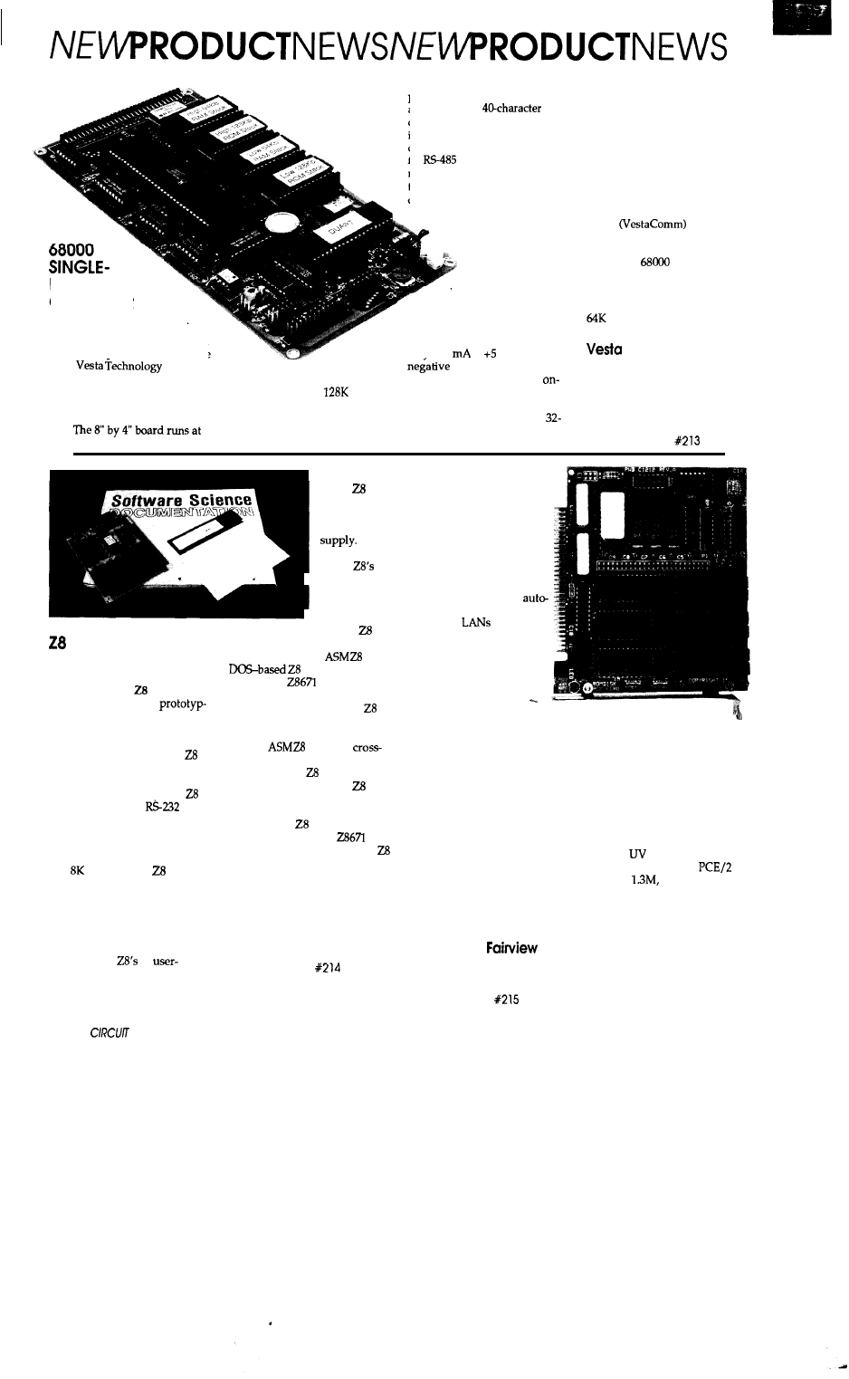
port, ports for a 4 x 5 keypad,
and a Cline by
LCD
display provide easy application
interfacing. Two serial ports, one
configured for RS-232 and one
for
with addressable
multidrop capabilities, allow ex-
tensive firmwaresupported
communications. All bus signals
are carried to an expansion
connector to support ex-
pansion boards with
BOARD
COMPUTER
a total of 16
megabytes of
memory and a
A low-cost single-board
computer featuring the Motorola
68000 microprocessor is available
variety of A/D,
D/A,
and I/O
configurations. The
board also includes a watchdog
timer to assure program control
of board status, and requires
onlv 650
at volts. A
from
Inc. The
computer contains an on-board
ROM-resident Forth develop
ment environment to facilitate
product development.
either 8 or 16 MHz and provides
socketing for up to
of
battery-backed RAM and up to
256K of ROM. A battery-backed
real-time clock, a parallel printer
voltage generator for
the RS232 port is provided
board.
The development language
in ROM is a direct-threaded
bit (address and data) extended
version of Forth-83 with multi-
tasking and assembler capabili-
ties. The language also provides
for autostart of ROM-resident
application code. The board
requires only an IBM PC and an
EPROM programmer for a com-
plete development system. A
PC-resident communications
package provided with the
board
permits use
of the PC’s disk to transparently
store and download code and
data to the
board while
acting as a console to the 68000.
The board sells for $295 in
single quantities and includes
of RAM.
Technology, Inc.
7100 West 44th Avenue,
Suite 101
Wheatridge, CO 80033
(303) 422-8088
Fax: (303) 422-9800
Reader Service
Proto-
Quick
board needs
only a single
5-volt power
Proto-
I
Quick
application
development
I
tools include
the Software
DEVELOPMENT
SYSTEM
ProtoQuick is a
microprocessor-based
ing and application development
system. The 4.5” x 6” single-
board computer and prototyping
board is based on the Zilog
microprocessor chip. Along with
nearly 12 square inches of
prototype area, ProtoQuick
has EPROM, RAM,
serial
communications, and a decoded
S-position DIP switch. Standard
28pin EPROM and RAM sockets
support up to 32K of EPROM
and of RAM. The single-
chip microprocessor provides six
vectored interrupts, two
counter/timers, as well as bit,
nibble, and byte-wide TTL I/O.
The RS-232 interface operates at
standard rates up to 38,400 bps
and all of the
14
configured I/O lines are
available at the prototype area.
Science
operating system in EPROM,
Software Science’s
MS
cross-assembler,
and Zilog’s
BASIC/Debug
BASIC-in-ROM CPU chip.
At $99.00, ProtoQuick
comes completely assembled and
ready to run with the Software
Science
MS-DOS
assembler and a copy of the
complete Zilog Technical
Manual. The ProtoQuick
board with parts list, assembly
drawings, operating system in
EPROM, and technical
manual is $39.00. The
BASIC-in-ROM version of the
chip is available separately for
$19.00.
Software Science
3750 Roundbottom Rd.
Cincinnati, OH 45244
(513) 561-2060
Reader Service
REMOTELY
PROGRAMMABLE
ROMDISK
A solid-state disk and drive
emulator that enables IBM
PC/XT/AT and compatible
computers to be used as
diskless terminals with
booting and special safe-
guards for
and other
networks is available from
Curtis Inc. The ROMDISK
FERO includes security
features to allow
operation of
terminals without _
mechanical disk
drives and provides solid-state storage for DOS and application
programs in the user terminal. LAN utilities enable the unit to be re-
motely erased and reprogrammed from a supervisory terminal on the
network without intrusion of the terminal. The unit can also be
incorporated as part of a home security system with a master control
system updating remote terminals as required.
The ROMDISK FERO is capable of emulating standard 3.5” and
5.25” diskettes up to 720K of storage. The unit uses flash EEPROMs
that are electrically erasable and programmable or standard ultravio-
let erasable EPROMs that have been programmed on a program-
mable model for read-only operations.
The ROMDISK FERO lists for $279 with
EPROMs and $319
with flash EEPROMs. Other models include the ROMDISK
which emulates 3.5” and 5.25” diskettes up to
programs
EPROMs or flash EEPROMs, and dual operation by emulating a sec-
ondary diskette with a battery-backed SRAM daughter board.
Curtis, inc.
2837 North
Ave.
St. Paul, MN 55113
(612) 631-9512
l
Fax: (612) 631-9508
Reader Service
12
CELLAR INK
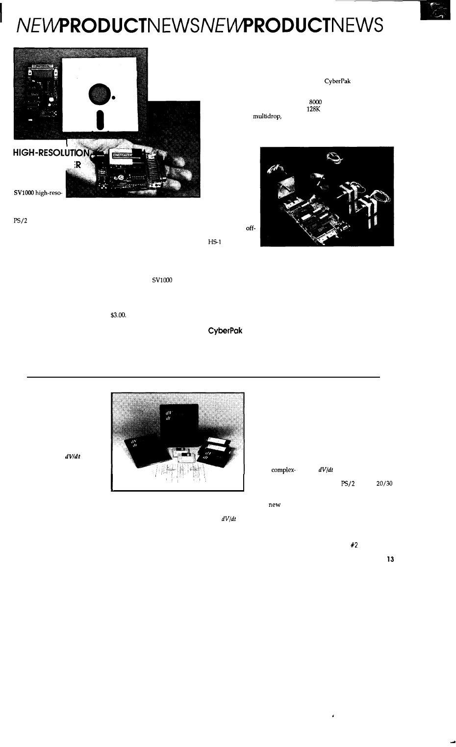
VIDEO DIGITIZE
The
Colorburst
lution video
digitizer plugs into the parallel
port of any IBM PC, XT, AT, or
compatible and can capture
video pictures from TV cameras,
VCRs, or other composite video
sources. Applications for the
compact 2” by 3” unit include
desktop publishing, inspection,
computer animation, and pattern
recognition.
Two modes, both with 256
gray levels, provide either
640x480 or 320x200 resolution.
Pictures can be displayed on
CGA,
EGA, or VGA monitors,
saved to disk with menu-driven
software, or exported to other
programs via the “grab” or
“freeze” utilities included with
most desktop publishing and
paint programs. Capture time is
10 to 20 seconds, depending on
resolution, and the unit runs
from any TV camera, VCR, or
video input.
The included software
provides simple menu-driven
setup, picture load and save
routines, and features built-in
diagnostics to check both the
video digitizer and the input
video source. Contrast, bright-
ness, sync, and unit on/off are
also controlled by software.
The Colorburst
sells for
under $90.00 and a packaged
version with a printer bypass
switch is also available. A dem-
onstration disk is available for
Colorburst
P.O. Box 3091
Nashua, NH 03061
(603) 432-2001
Reader Service # 216
CUSTOMIZABLE
MULTIAXIS INDEXER
A complete stepper-motor-based motion-control system can be
created with the High Stepper System from
Co. The HS-1
Multiaxis Indexer supports axis limit inputs and provides step and
direction control signals simultaneously for up to four stepper motor
drivers. It has a maximum step rate of
steps per second and a
total nonvolatile memory capacity of
bytes. The HS-1 permits
RS232 or RS-485
which allows an expanded system to
control up to 64 motors at once. It can be programmed as a stand-
alone unit or can receive commands from a host PC or any other
device supporting serial data communications.
The com-
mand set is
composed of over
76 different com-
mands including
basic arithmetic;
high-speed
looping, calls, and
branching; 208
variables; and
general-purpose
I/O functions
addressing 48
board pins. The
can be
directly interfaced
to user control panels involving matrix keypads, BCD switches, and
LCD and VF displays. Isolated firmware drivers facilitate support for
new interface devices. IBM PC software tools provide communica-
tions, program download and upload, custom ramp generation/in-
stallation, and so on.
The price of the HS-1 system starts from $299.00 each in single
quantities. Free technical application notes including hookup
schematics to various brand stepper motor power amplifiers, matrix
keypads, LCD displays, and thumbwheel switches are available on
request.
Co.
251 S. Frontage Road, Suite 23
Burr Ridge, IL 60521
(800) 328-3938
l
Fax: (708) 654-4027
Reader Service 44217
TIMING DIAGRAM
ACCELERATOR
The analysis and optimiza-
tion of digital circuit timing dia-
grams can be accomplished
faster and more accurately with
a new software product from
Doctor Design Inc.
(the
mathematical designation for ac-
celeration) creates a unique
approach to circuit design by
integrating waveform sketching,
circuit modeling, timing
analysis, and verification into a
single package. It allows design
engineers to rapidly sketch and
change timing diagrams, define
time relationships between
events, automatically reanalyze
easily analyzed,
and bus timing
requirements
can be verified
without
captured
schematics for
processing. This
“preprocessor”
feature does not
restrict the
circuit
ity or require
behavioral
models, and
does not require
design changes, and perform
upgrading each time a
“what-if” calculations. Any
processor is released.
circuit, including those with
generates clock
complex microprocessors or
signals automatically, performs
custom components, can be
common path and common part
analysis, defines propagation
symbols, and verifies setups,
holds, pulse widths, and cycle
times. It provides automatic
timing diagram documentation
by outputting the finished
product to laser and graphic
printers. The program also pro-
vides a user-friendly interface
with pull-down menus and
mouse-based icon selection.
lists for $695 and runs
on the Apple Macintosh, IBM
PC/AT, IBM
models
and compatibles.
Doctor Design, Inc.
54 15 Oberlin Drive
San Diego, CA 92121
(619) 457-4545
Fax: (619) 457-l 168
Reader Service 18
August/September 1990
Aristo Computers, Inc.
6700 SW 105th Avenue, Suite 307
OR 97005
(800) 327-4786
Fax: (503) 626-6492
Reader Service X219
PORTABLE SIMM/SIP MEMORY
MODULE TESTER
SIMCHECK,
the first portable SIMM/SIP tester that
tests the memory module as a complete unit, has been
announced by Aristo Computers Inc. The unit tests all the
standard SIMM and SIP memory modules with 8 or 9 bits
of
or
devices. It is a stand-alone
tester with a high-speed
processor to control the
proprietary test routines. Access time is measured down to
20 nanoseconds and a unique CHIP-HEAT mode warms
modules for temperature-dependent measurements.
A two-line alphanumeric LCD display provides the
operating instructions and test results, including identifica-
tion of bad chips, access time, and module type and size.
All chips are tested simultaneously and an Auto Loop Test
allows testing to be repeated, using changing data patterns
and different algorithms, without user supervision. The
test programs reside in a socketed EPROM to allow for
future enhancements. Errors are traced to specific chips or
module wiring problems.
Zero-insertion-force sockets are used for both the
SIMM and SIP modules, and full power protection using
automatic current limiters and two programmable voltage
sources is included. The unit measures 5” x x 1.5” and
weighs under two pounds.
SIMCHECK retails for
$995
and comes with a
money back guarantee and one-year warranty. A full year
of program upgrades is also included.
PC-Based Logic Analyzers
Sophisticated Logic Analysis
a’, Unsophisticated Prices
ID160 (50 MHz) for $695
*ID161 (100 MHz) for $895
MHz or
100 MHz Sampling
l
Trace Buffer
l
Operation *Multi-Level Triggering *State Pass Counting
*Event Timer/Counter *Performance Histograms *Hardcopy
*Disassembles popular
micros
much more
30 Day Money Back Guarantee
INNOTEC DESIGN, INC.
6910 Oslo Circle, Suite 207
Buena Park, CA 90621
Tel: 714-522-1469
Announcing the
Industrial Controller
and
Peripherals
Our expandable controllers get your projects up and running
Features include:
Self-contained
vertical stacking bus
AT style
serial port
Built-in watchdog timer
Built-in power fail detection
battery backed RAM
EPROM
Small X 3” board size
All address and data pins available on 80 pin bus
16 line decoder for memory mapping
Surface mount technology utilized for glue chips
Voltage regulator
VDC)
Reset button
High quality dry film solder mask pc board
Industrial temperature range available
Diskette of assembly language support
included
hour support bulletin board
Stacking bus peripherals include:
@Breadboard with screw terminals and
VDC regulator
BRD
(20 X 4 char.), 16 button keypad interface latched I/O
LCD
l
Backplane with all power supplies and screw terminals for bus
BPS
l
82C55 parallel
board (total of 9 parallel ports)
*Multichannel A/D and D/A board (12 bit resolution)
WB-lAD*
4 20
current loops with surge protection
l
Denotes cards
in the near future.
A
Product
Company
(918) 251-8031 BBS
Service
14
CELLAR INK
MODULAR MICROCONTROLLER AND PROTOTYPE KIT
High-performance real-time
control, with such applications
as high-speed closed-loop
tion control, midrange digital
signal processing. and intelligent
data acquisition, can be achieved
with the
Modular Microcontroller and
Prototype Kit from
Corp.
The 3.5” by 3.5” unit features the
Intel
embedded
controller operating at 16 MHz,
is software supported by an
line monitor controlled via an
IBM
or compatible,
and provides
oriented
programs. The
MICON-196KC can also be used
as an EPROM programmer for
parts and features a 64K
memory
module with customized
memory mapping.
The MICON-196KC
includes eight ADC channels
with sample and hold at a
rate, four high-speed capture
inputs
l-microsecond
resolution, six high-speed out-
puts for pulse and waveform
5.25” diskette, and user’s manual
with applications-oriented
tutorial programs. The system
sells for $279.00. A power and
communication hardware kit,
the PSMICON-2, consisting of a
compact power supply and
cables, sells for $89.00; and an
8096 assembly language
tutorial sells for $78.00.
Corp.
5270 Elvira Road,
Bldg. 104
Woodland Hills, CA 9 1364
(8 18) 348-4992
Fax: (818) 348-0960
Reader Service X220
generation, one DMA channel,
The MICON-196KC consists
three pulse-width-modulated
of CPU, memory, bus, and
outputs
one full-duplex
prototype modules, two monitor
RS-232 serial port, and five
EPROMs, two
for memory
I/O ports.
configuration, a PC interface,
EPROM
The PROM KING emulates EPROMS, saving both time and
money during your development cycle. Programmable in
seconds via your PC printer
or any computer RS232
port, it can emulate most
devices.
l
bit devices
l
8-256 bit downloads
l
High speed download:
l
Easily expandable:
-Universal RS232
-4 EPROMS per unit
-PC printer port
to 8 units
l
Menu driven software
l
Battery backup
Also programs like
a real EPROM
$599 for 150nS units with 256K bits. Ask for
of other options,
Made in USA by
BOX 239
l
176
12
VDC GEAR MOTOR
GEL
Powerful little
40 RPM
12 Vdc. (no load).
32 RPM with load.
at
voltages with
speed and torque.
6.3 pound inches torque. Stall: 27 pound
inches. 3.1’ long X 1.375” diameter.
Shaft: 6.167” dia.
OPTO-ISOLATORS
Isolator.
ohms. On
500K ohms. 2000 volt isolation.
Forward voltage: 2 Vdc. CATW
each 10 for $22.00
Signal applied to
the input is coupled by
of light to
isolated photo
cell. High
12 Vdc.
$1.50
SENSOR
U shaped
with
opening.
ENCLOSURES
ABS instrument
Matching
and rear panek.
PC
and two sets of
vertical mounting slots for front and rear
sub panel PC boards. All enclosures are
6” wide X 6
deep. Available in black.
ivory. blue. and beige.
color.
FRONT REAR PANEL HEIGHT
2
CATX
oo
2
ME-B
75 each
3 ’
M B - C
PHOTOFLASH CAP.
CE
210 MFD 330 V
3.79”
X 1.1’ high. New.
with 1.4’
and red
leads soldered to the terminals.
PPC-210 $2.50 each
10 for $22.50 100 for
STEPPING MOTOR
17 Vdc 23.25 ohm
P.M. motor.
7.5 degrees per
2.25” dia. X
thick.
3.25’ dia. shaft. 6 wire leads.
August/September 1990
15

Universal
Cube
l Universal
Cube
a custom designed enclosure for
Micromint
applications. Supports
P.S.
l Dimensioned for the Micromint
family, 5’ footprint.
l Constructed from 15 Gage brushed black-anodized aluminum.
l Convertible box 7
3 board stack
. industry standard connector cutouts on faceplates.
l 4-40 machine screws and 4-40 PEM nuts for assembly
l Optional 0.531’ standoffs available for securing
stack’.
$99.95
Headlight Kit 7 LED’s + driver, power reset
all on a single
board
LED supported). Mounts in
Cube faceplate
$29.95
Communication Kit A
of
sockets configurable for MC-NET
dual serial
on a board. Mounts in Universal
Cube faceplate.
$29.95
Integrated Vessel Information Corporation
V i
871 Via
Unit
California 93010
(505) 3595870
ELECTRONICS
1.
Exclusive items at good price.
2. Unique items at better price.
A DIVISION MING
Popular items at the best price.
5 SECOND EPROM ERASER
Revolutionary product
super energy output
Saves time money
The most desired product
Patented design
MING
$249.99
_
_
DISK CARD
For diskless PC station
Load DOS file instantly
Battery back-up for
Watch-dog time; rebooting
$ 1 7 9 . 9 9
$199.99
REMOTE CONTROL SYSTEM
19683 digital coding
2 tiny transmitters
Dry contact relay output
confirming signal
FCC approved
ZEMCO SA432
E ORDER LINE
977 S.
Meridian Ave., Alhambra, CA 91803
Tel:
(818)
Fax: (818) 576-8748
VISA MASTER CARD ACCEPTED
Computer
For Programmers,
Consultants, Retailers, Developers,
Hardware/Peripheral Manufacturers Any Computer Entrepreneurs!
Problem: One of the world’s largest chipmakers forfeited all
legal protection for a revolutionary new product
due to a SIMPLE copyright law mistake!
Result: Over
in lost revenue!
Solution: THIS PROGRAM!
Order NOW!
Call 24 Hours!
Most Cards Accepted!
Full Annotated Text of Laws,
Court Cases and Government
Regulations +
Mini-Seminars
Legal Document Generator Using
A.I. with More Than 40
That Are Valid In All 50 States!
Employer/Employee Relations
Computer and Software Leasing
Credit and Collections
Contract Bidding
Semiconductor (Mask) Work Protection
Arbiiration
O
N E
L
A W S U I T
C
A N
R
U I N
Y
O U R
W
H O L E
Fringe Publishers, Inc.
Box 796,
FL
32707
Issues Relating to Computers
Patenting vs. Copyrighting
Written by a computer-literate attorney
PRIVATE BBS COMPUTER EMPLOYMENT EXCHANGE. UPDATES
System Requirements: MS-DOS XT, AT, 386
RAM, Hard Drive
U.S. Copyrights
International Copyrights
Uniform Trade Secret Law
Patent Law
Trademark Law
Computer Crimes Law, Federal
Computer Crimes Law, all 50 States
Warranty Disclaimers
Military Computer Acquisition Regulations
Legal Liibilii of Computer Professionals
Beta Testing Law
BBS Laws
16
C I R C U I T C E L L A R I N K
FEATURE
ARTICLE
I he increased use of
imaging systems in the
world of microcomputers
is primarily due to emerg-
ing low-cost instrumenta-
tion Cameras, scanners,
high-resolution monitors,
mass storage devices,
video printers, image
capture-digitize-display
boards, as well as ad-
vanced packages in im-
age synthesis and process-
ing software, have be-
come generally available
at affordable prices. As a
result, there has been
growing popular support
for a whole array of imag-
ing applications. The use
of these imaging technolo-
gies also implies the use of
some very sophisticated
data handling utilities if you
need to transfer the ‘im-
aged” data at reasonable
rates across some network
or modem connection.
18
CIRCUIT CELLAR INK
Illustration by Lisa Ann Ferry
Image Compression for High-Speed
Network Transmission
I know! I’vebeenespecially aware
of this problem since it takes me over
15 minutes to transfer a 512 x512-byte
image over my modem at 2400 bps.
The old saying, “a picture is worth a
1000 words,” is underestimating the
truth.
With the growth of imaging ap-
plications in networked PC systems,
techniques that enhance “image data”
transfer have been high on the R&D
list. Image data compression has be-
come an integral part of imaging sys-
tems technologies. As a result, there is
intensive ongoing research in such
areas as digital mapping, document
archival and retrieval, electronic pub-
lishing, engineering drawing, image
communication, medical imaging,
cataloging, picture ID systems,
of-sale systems, prepress imaging,
remote surveillance, teleconferencing,
telemetry, teleradiology, image syn-
thesis, animation, and artificial vision
within AI and robotics, Each of these
fields has different image compres-
sion requirements.
Of course, the choice of compres-
sion mode depends highly on the type
of image data. Using a data compres-
sion utility that is truly designed to be
universal is highly desirable. It should
be able to handle different types of im-
age data which support a wide variety
of applications. To that end, I’ll de-
scribe a simple programmable image
compression system which can com-
press and expand single-frame com-
puter-generated graphics images
(monochrome or color) as well as
scanned documentsand video images.
It is programmableby thegeneral user
whocan’tafford
the
fancy
“hardware”
compression card. My method uses a
very simple, but universally applied
compression technique which is based
the applicationof a Fourier transform,
an image is decomposed into its fre-
quency components. These compo-
nents are then selectively chosen
(banded) according to their contribu-
tion to the visual content of the origi-
nal image. All components that have
little effect on the image are elimi-
nated in order to effectively reduce
the size of the information set neces-
sary for a reasonable reconstruction.
These “necessary” components are
values forencodinginto a binary-word
data stream. The data stream is then
compressed by the elimination of re-
dundancy and multiple spatially ad-
jacent zeros for transmission, and re-
constructed by reversing the proce-
dure.
IMAGE DATA TYPES
Different digital image data types
are generally categorized and defined
in
theircolor content; whether
the image is
monochrome
or
color and
if it is colorizcd, whether the color is
classified as true or mapped color.
Figure
1 -The
techniqueismosf
useful on images with a high degree of
local pixel correlation.
For monochrome images, the
number of bits per pixel fully defines
the image value, or gray level; with
typical systems employing
one
of three
gray
level schemes, either a single
binary image composed of only two
gray levels, an 8-bit system composed
of 256 individual gray levels, or a
bit, 4096 gray level format. With the
addition of color, the number of bits
necessary to encode information in-
creases. For example, if we consider
an RGB true color scheme, we need to
define an n-number of bits for each of
the three individual components per
color pixel. In a mapped color system,
each pixel value is designed to repre-
sent an index into a larger palette,
with a small number of key colors or
(RGB triplets) being selected from the
palette for a given application. Here,
mapping is implemented through the
a look-up table, with the result-
ing color value containing so many
index bits and three n-bit color com-
ponents. As a result, true colors are
typically represented by
word
using 8 bits for 224 different combina-
tions
or 5-bit words
representing 215 combinations (32,768
colors); while mapped color systems
usually employ an S-bit index with an
or 6-bit 3-word length palette, re-
sulting in 256 colors from a palette of
either 224 or218 (VGA) colors respec-
tively.
As a result of these high densities
in image pixel data bits, the major
decision lies not so much in what type
of data format is used, but whether
one implements a
or
controlled
qualify compression
technique. A
method of compression im-
plies that
the reconstructed
image will
be digitally identical to the original. In
controlled quality compression, the
image is reconstructed with reason-
able image quality but using less
August/September
19
Quality U.S.-manufactured cards
and software for single user, OEM,
or embedded applications.
differential,
AID
Programmable gains of
16
Three
timer/counters
Two
D/A outputs
40 Digital
lines
120 signals through a single slot!
Dedicated ground for each analog signal
Real Time Devices, Inc. designs and manufac-
tures a broad line of cost-effective industrial/
scientific interface cards and software for the
PC/XT/AT bus. Our commitment is to offer
only high-quality U.S.-designed and manu-
factured interfaces with emphasis on signal
quality and ease of use for OEM applications.
All our cards are backed by a one-year war-
ranty, and
NO-RISK return policy.
Call today to request your free catalog and
discuss your application requirement!
AD1000 X-channel
20
A/D;
sample
hold; three
timer/counters; 24 TTL
digital
lines.
$325
AD2000 X-channel differential 20
A/D;
sample hold; three
timer/counters;
prog. gain;
digital I/O
$495
AD100 l-channel single-ended
inte-
grating A/D;
$159
AD200
A/D; three
timer/counters: resistor-configurable
gains; 24 digital I/O lines.
$259
AD500 X-channel
integrating A/D; pro-
grammable gains of I, IO,
Extremely
stable, accurate sensitive.
$259
ADA100 Single-channel, differential input,
A/D;
D/A
output; pro-
grammable gains of I,
IO, 100. Plus
digital
lines.
$215
ADA300
X-channel H-bit 25 A/D;
sin
bit
D/A; 24 TTL
digital I/O lines
259
Fast-settling
-channel
D/A; double buffered
$2071495
TTL
compatible
digital I/O cards; NMOS
Opt.
buffers and pull-up
resistors
$1101274
TC24 Five
timer/counters;
pow-
erful
chip; 24 digital I/O lines from
NMOS 8255
chip
$218
ATLANTIS High-performance data acquisi-
tion software; foreground/background opera-
tion; maximum
rate;
supports hard
disk streaming; pull-down windows.. $250
Real Time Devices. Inc.
State
PA 16804
Phone:
FAX: 8
20
CIRCUIT CELLAR INK
formation during transfer. That is, the
compression ratio is enhanced at the
cost of image reproduction quality.
The compression ration (CR) is de-
fined as the ratio of b/c, where is the
number of bits per pixel in the original
image and c represents the bits per
pixel in the compressed image. For
example, if my 512 x 512 by 8-bit byte
image is made of 161,319 bits, in com-
pressed form, 8 bits/pixel and c =
then my compression ration is
0.61538 = 13.0. I have made my data
transfer 13 times faster using com-
pression. Of course, in the real world
I need to include time spent for com-
pression/decompression execution,
so I will actually realize a total trans-
mission factor on the order of 5 to 10,
depending on the form of the utilities.
Software implementation is the slow-
est compression technique, but using
a hardware compression board (such
as one structured around the Zoran
ZR34161 vector signal processor and
an Intel 80286 CPU), extremely high
factors are possible.
To give you one example of these
“hardware implemented” compres-
sion-transfer capabilities, consider an
image made up of 512 x 480 true color,
RGB 8-bit word pixels. An achievable
compression ratio for such an image is
Using Zoran’s card, this im-
age can be compressed in 4.7 seconds
and decompressed in 2.35 seconds,
resulting in a total of 7.05 seconds
needed for the compression/decom-
pression cycles. Now assume that our
network transfer information at 9600
bps and the total image contains 512 x
480 x 24 bits. As such it will take 614.4
seconds (or 10.24 minutes) for the un-
compressed version to be transferred.
Using the processor-based system
with a compression ratio of 24, this
same file transfer will only take 25.6 +
7.05 seconds (or 0.54 minutes). This
doesn’t include the time for loading
the image into and out of the frame
buffer for line transmission.
A PROGRAMMABLE DCT
COMPRESSION UTILITY
Reducing the amount of image
data stored or transmitted greatly
reduces the disk capacity or channel
bandwidth required in a system.
Unfortunately, as the quantity of the
information used to represent an
imageisdecreased, so is the subjective
quality of the image. Most
c s e t c o e f f i c i e n t s
c
d o
!
d i m e n s i o n o f b l o c k , N - 1 = 7
i f
t h e n
e l s e
c
c do 2-D DCT for
c
d o
d o
F
d o
d o
du =
* PI * 16
dv =
* PI * v 16
=
+ f
* c o s
* c o s
=
*
*
*
listing -One method for obtaining a 2-D
by using the forward application of the
two-dimensional DCT algorithm
sion algorithms must therefore make
a compromise between the transmis-
sion rate (compression ra and their
ultimate image quality. This rate-ver-
sus-quality tradeoff has led to the use
of a popular method of image com-
pression called the Discrete Cosine
Transform
technique, which
minimizes this compromise. The DCT
(and its inverse,
is widely used
for compressing motion and
frame coding and has been proposed
as the international video-telephony
The
technique is most
useful on images
a
degree of
local pixel correlation. The technique
involves the partitioning of an image
into 8 x 8 blocks (defined here
with each block being acted upon by a
two-dimensional DCT. The output of
the DCT procedure is then passed
sen to trade off perceived quality
against bit rate and then passed to the
encoder for coded bit-stream
construction, as
shown
in Figure 1.
do
the dimension of the N
N hlnr
if
c = 0.:
else
,
do m=O,N-1
for each sample input
d =
* PI * K
X(k) = X(k) +
X(k) =
* C
listing 2-An alternate method for obtaining a 2-D DCT is to perform the 1-D DCT eight
times in each
forward and inverse (shown below) transforms are used.
Here, x(m) represents the input samples and X(k) is the resulting -D DCT output, with
for most applications.
do
the dimension of the N x N block
do
for each sample input x(m)
if
then
C = 0.7071068
else
d =
*
PI * K
=
+
* C *
x ( m ) = x ( m ) *
listing
inverse I-D DCT is used
the forward 1-D DCT (above) to obtain a 2-D
DCT. Here, x(m) represents the output pixel values and
is the input.
standard. DCT compression also has
the advantage of being cheaper to
implement than most other tech-
niques, such as
coding
since it renders an image into fre-
quency components, a process that
can be achieved by a single pipelined
operation. Forimagesof
lution, say 350 x 250 pixels, a disk
bandwidth of about 1.0 megabits/
second produces a good reconstructed
image. This corresponds to about 2.5
minutes of full color motion video
from a 20-megabyte Winchester disk
and over twenty times that figure from
current technology CD ROMs.
The output of a 2-D DCT opera-
tion,
can be obtained using two
different methods. The first is achieved
by the forward application of the
dimensional DCT algorithm
shown in Listing 1, with
being
the input 8 x 8 pixel block. For an in-
verse 2-D DCT
apply the fol-
lowing equation:
=
x
X
16
16
FAST TEST
DRAM
RESOLUTION
ACCESS SPEED VERIFICATION
80 ns.
180 ns. (Std.)
45 ns.
110 ns. (Fast)
4M
Option
Add $
AUTO-LOOP
Continuous Test 6.25
DAPTERS:
Tests
1 M 4M Devices
8 or 9 Bit versions
ADAPTER
Tests
All Bits Simultaneously
1 M 4M Devices
4 X ADAPTER
Tests 64K 256K By 4 Bit Devices
AC ADAPTER
$
Regulated
1 Amp.
FREE
DRAM NEWSLETTER
COMF'UTERDOCTORS
9204-B Baltimore Boulevard
College Park, Maryland 20740
IN U.S.A.
PATENT
August/September
2
1
Introducing
EXPLORER
Stock Market Forecasting
Systems
Inc. presents
Explorer, a neural network tutorial that
provides the novice user with a method
neural network theory as well as an
environment in which to build practical
applications. Available on both the MAC
and
Price $199.
The
product line is
currently used in:
l
Oil
l
Medical Diagnostics
l
Industrial Inspection
l
Credii Approval
l
Process Control
l
Insurance Underwriting
l
Economic Modeling
l
Noise Filtering
l
Signal
l
Fmud Detection
l
Bankruptcy Prediction
l
Targeted Marketing
Penn Center
Bldg. Suite 227
Pennsylvania 15276
2 2
CELLAR INK
do
do
if
then
=
g +
else if
then
=
else if
then
Ming
4-A
way of quantizing the output of the DCT can be realized through the
use of the quantization algorithm shown here.
The second procedure for obtain-
ing a 2-D DCT performs the 2-D DCT
by using the 1-D DCT eight times in
each dimension according to the algo-
rithms from Listing 2 and Listing 3.
and k represent indices of line
along a row or column of the
block,
and
THE
PROCESS
Next, each of the 64 FDCT output
coefficients of
are quantized by
a uniform quantizer. Usually, the
FDCT block of spectral components
forms a sparse set with the majority of
the energy concentrated in the
frequency corner of the block. Special
care must therefore be taken with the
choice of a frequency threshold and
the quantization step-size if we are to
maintain reconstruction quality. In
principle, a quantizationmatrix
to be the perceptual discrimi-
nator for the visualization contribu-
tion of the cosine basis function of
frequency
for the intended color
system, display device, and viewing
distance; with multiple Q matrices
being created for different color com-
ponents since their perceptual contri-
bution varies. A simpler way of
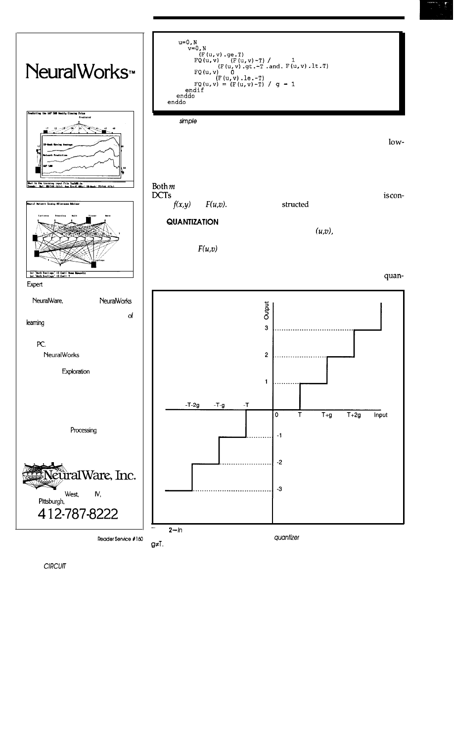
Figure
the quantization algorithm shown above, g can be varied depending on the
desired transmission bandwidth. Here, the
function is represented for the case
the output of the DCT can be
term and 63 zero terms, for a
alized through the use of the
sion ratio of
In addition, many
zation algorithm in Listing 4 (for a frequency components are small and
single threshold and step size), where contribute little to the overall image.
is the step-wise quantized They are below the visual threshold
data,
is the output of the DCT and are truncated in the quantization
function, is the threshold at which
process. These now zero components
represent the majority of the
available image compression.
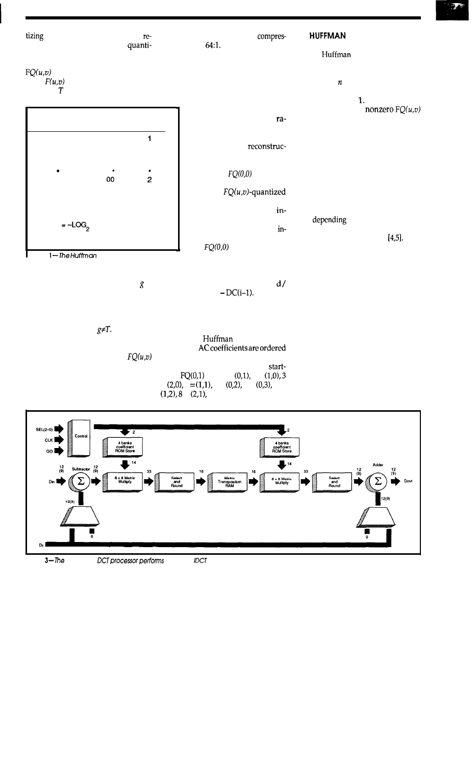
Coefficient
Huff man
Number
Value
Code
of
Bits
For higher compression
tios thequantization step size
1
1
and threshold can be raised.
2
011
3
For proper
3
01000
5
tion, prior to the original bit
4
01010
5
compression, the “DC”
zeros
coefficient,
is usually
treated separately from the
with
the number of bits b required to represent
other 63
“AC” coefficients (within the
a value of probability
P
being,
matrix,
rows represent
b
P
creasing horizontal fre-
quency, columns represent
where b is rounded to the next higher integer.
creasing vertical frequency,
and
is the DC term).
Table
technique uses
variable-
The Quantized DC term from
length codes to represent the values of the quan-
tized DCT string sequence.
block’ i is differentially en-
coded with respect to the DC
the output is forced to zero, and is term from the previous block i-l:
the quantization step size. Note thatg dt DC(i) = DC(i)
Since 11
can be varied depending on the de- bits are sufficient to represent any
sired transmission bandwidth. Figure quantized DCT coefficient (either AC
2 is a representation of the quantizer or DC), 12 bits are sufficient to repre-
function for the case
sent all possible differential terms.
Since most images do not contain
all frequencies, as a white noise image
would, many of the values of
will be set to zero. This represents the
redundancy within an image and its
available compression. For example,
a pure gray image would have one
DC
Prior to
Coding, the 63
quantized
from their 2-D matrix into a 1-D se-
quence, in a “zig-zag” manner
ingat
(i.e., 1 =
2 =
=
4
5 =
6 =
7 =
=
etc.)
THE
ENCODER
The
technique uses vari-
able-length codes to represent the
values of our quantized DCT string
sequence (of bytes), according to the
frequency of occurrence of the value
as shown in Table
If most of the
coefficients have the value 1 or 2, then
coding them can approach two bits
per coefficient (one bit for the value
plus one bit for the sign). Since the
probability of a zero is even higher
than a one and because zeros are more
likely to occur in the high-order coef-
ficients, a simple code can be created
to represent multiple spatially adja-
cent zeros. Here, additional enhance-
ment of the compression ratio is pos-
sible
on
the truncation and
ordering scheme chosen to optimize
adjacent zero specification
HARDWARE IMPLEMENTATION
Use of the DCT utility for com-
pression purposes has become very
popular. Since its introduction as an
industry standard, many DCT-specific
processors have been created and
several PC image compression boards
have been designed.
One such DCT processor is the
IMS A121, shown in Figure 3. It per-
forms DCT and IDCT by the classical
matrix multiplication method using a
distributed arithmetic architecture
which is ideal for cheap dedicated
arrays with fixed coefficients stored in
Figure
IMS A
121
DCT and
operations on a single chip.
24
CIRCUIT CELLAR INK
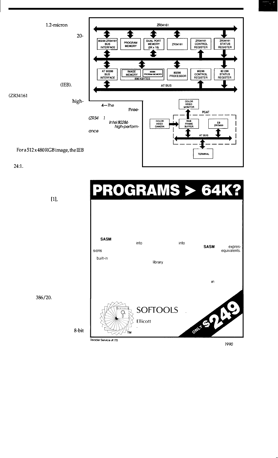
preprogrammed ROM. The device is
manufactured in
CMOS
and contains 185,000 transistors. The
most current specification uses a
MHz clock, which corresponds to a
processing rate of 320 MOPS. As such,
it can calculate a transform in 3.2
microseconds.
A very effective image compres-
sion card for your PC is currently
available from Zoran Corporation of
Santa Clara, California, called the
Image Engineering Board
It is a
three-bus dual-processor system
vector signal processor and
Intel 80286 CPU) optimized for
performance and Fourier domain
processing, and operates in an AT en-
vironment. The memory resources
support processing of a 512 x 480 RGB
image, and can be flexibly allocated as
data, image, or program memory. A
2K DPR supports simultaneous proc-
essor operations (see Figure 4).
has demonstrated a compression time
of 4.7 seconds at a compression ratio
of
This time includes DCT, en-
coding, and image transfer from AT
frame buffer to IEB and back. The
measured decompression time for the
IEB is 2.35 seconds. For more details
on this board, I refer you to a paper by
I. Livny and D. Seltz
“Vector Sig-
nal Processor-Based Image Process-
ing Applications,” presented this last
October at the Boston Electronic Im-
aging ‘89 Conference.
BUS
80286 BUS
Figure
Zoran Image
Engineering Board is a
bus &al-processor system
16 vector signal proc-
essor and
CPU)
optimized for
and Fourier domain
processing.
IBM
AND ON TO THE REAL WORLD
I don’t know about you, but I’m
an impatient man. I dislike staring at
my CRT and waiting for the end of an
image file transfer. That’s what got me
into the compression business in the
first place. Since I prefer not to pur-
chase fancy “hardware,” I developed
the need and opportunity for looking
into how I could implement my own
image compression/decompression
utility on my
I built a simple
FORTRAN code based on the DCT
technique described above. It’s not
bad. It speeds up my modem transfer
time by about a factor of eight; so, I
only hang around for about two min-
utes instead of 15-20 (for an
August/September
25
Auto-MMU Support Is The Answer.
SASM-Advanced Macro Cross Assembler
SLINK-Advanced Linker
Softools,
Inc. introduces a relocating macro assembler and linker package that
offers many features for the embedded programmer at an affordable price. It supports the
64180, 280, 8085, and 2280 processors.
also supports the 64180 MMU for automatic control of programs larger than
64K by making “long” calls
segments not mapped
the address space. It also includes
many pseudo-opcodes for close compatibility with other assemblers.
accepts
that use operators common with other assemblers as well as C operator
SLINK is able to resolve any expression if SASM is unable to obtain a result. SASM includes
a
MAKE facility which supports dependency file checks. It allows you to use one
source file to generate a multi-module
file. In addition, SASM generates full source-level
debugging information for each source file including the source name, include files, line
numbers, public symbols, and local symbols.
SLINK output is compatible with In-Circuit Emulator (ICE) source-level debugging, and
also generates binary or Intel HEX files and has the ability to divide output into multiple
ROM image files. It supports named segments which may be up to 64K length each,
and may be linked to reside at one physical address and executed at another. Any
banked or MMU controlled program requires this feature to locate code effectively.
SLINK also allows the exclusion of physical address ranges in order to leave holes
in the output file.
INC.
8770
Manahan
Drive
City, MD 21043
301-750-3733
Figure
the original5
12x8-bit
test image that /compressed, transmitted, and then reconstructed. The
reconstruction is shown in
Both
and
were zoomed by a factor of four so a quick comparison of ‘visual detail’
between the
original(b) and the reconstruction
can
easily be
made. Note the slightblurring. which /expected, because
the quantization
to its limit. Of course, the nature of the original image helped; it started out with 7
1% of
its pixels set to a gray level
This
resentednull
of the image. The remaining 8 x 8 blocks were DCT quantized and then the whole image was
encoded. achieved a compression ratio (for this specific example) of 2 1.34: I.
monochrome
512 x 512
graphics
im-
age transfer). The only real difficulty
that I encountered was in modifying
the
encoding procedure to
improve reduction of redundancy in
coefficients, especially zeros. So, when
you get to this point, have
fun.
I found
several schemes suggested, but in the
end I just winged it, but with some
success. My reconstructions are for
the most part fairly good, but there is
a little blurring of sharp distinctive
edges if I set my visualization fre-
quency band too narrow (see Figure
5). I usually found I eliminated too
many of the high-frequency compo-
nents in the quantization process.
at it. Writing your
own code isn’t too difficult or compli-
cated, just be sure to use some sophis-
ticated file access techniques to mini-
mize image data access from your
Chris
has a Ph.D. in
experimental
nuclear
physics and is currently working as a
at a national lab. He has exten-
sive experience in computer modeling of
tal systems, image processing, and ar-
tificial intelligence.
IRS
201 Very Useful
202 Moderately Useful
203 Not Useful
REFERENCE5
1. Livny, and
‘Vector Signal
Processor-Based Image Processing Ap-
plications,’ Advanced Printing of Pa-
per Summaries, Electronic lmagin
p 179-l 84, 989
‘89,
2.
and
Sub-
band
of Images-Comparison
with DCT.’ Signal Processing, 4, 1988.
3.
A., ‘A Method for the Con-
struction of Minimum Redundancy
Codes,’
IRE, 40 1098-l 101 (1952).
4. Dubois, E. and J.L.
‘Encod-
ing and Progressive Transmission of Still
Pictures,’ IEEE Trans. Commun., vol
COM34, pp 310-319.
5. Dubois, E., Y. Rahmouni, and F.
‘Experiments on Image Coding with Dis-
tortion Below the Visual Threshold,’ SPIE,
pp
26
CELLAR INK
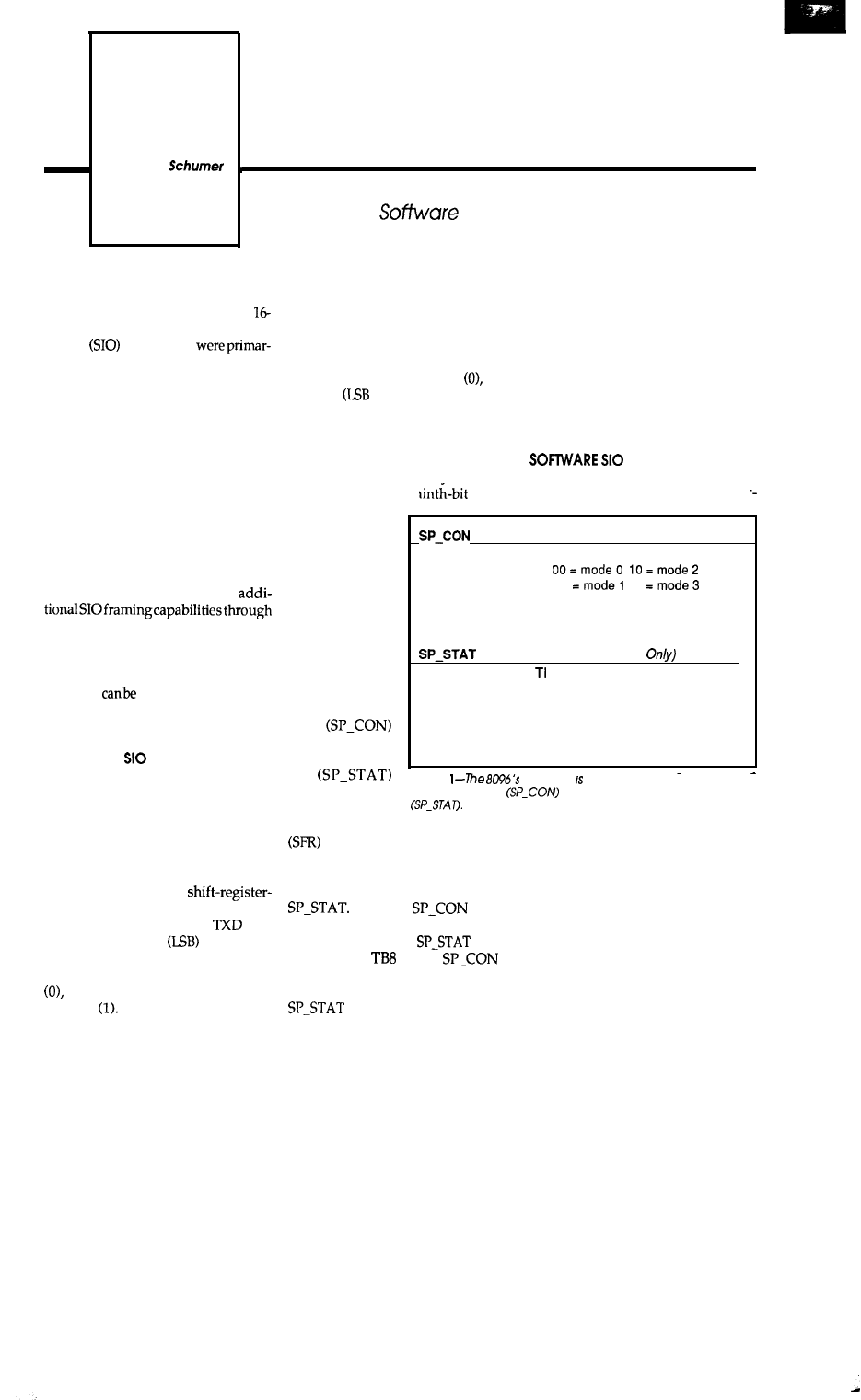
Extended Serial
Alfred L.
Communications on the 8096
Increase the Utility of these Ubiquitous Chips with
Simple
C
W
hen Intel designed the 8051
embedded controller, and later its
bit cousin the 8096, their serial input/
output
capabilities
ily intended for host and multiproces-
sor communications. Today, how-
ever, embedded microprocessors are
being used in ways not originally
envisioned, including SIO input fil-
tering, often
to
peripheral devices with
fixed and unusual framing character-
istics. (In asynchronous serial com-
munications, framing denotes the
number of start, stop, data, and parity
bits.)
This article examines the serial
communications capabilities of the
8096 (and by default the functionally
identical 8051) and develops
a collection of C language functions.
In addition, I’ll discuss SIO deficien-
cies in Intel’s implementation of the
8096 standard library and how these
functions
incorporated into em-
bedded C applications to provide
robust serial communications.
HARDWARE
MODES
The8096 provides
four
SIO modes
in hardware including one synchro-
nous and three full-duplex asynchro-
nous modes, one of which is dedi-
cated to multiprocessor communica-
tions. Mode 0 is a synchronous mode
commonly used for
based I/O expansion in which eight
bits are shifted out to the
pin,
least-significant bit
first. Mode
1 is the standard communications
mode consisting of ten bits: a start bit
eight data bits (LSB first), and a
stop bit
If parity is enabled, an
even parity bit is sent instead of the
eighth data bit and checked on recep-
tion. Mode 2 is the asynchronous
ninth-bit recogni tion mode commonly
used for multiprocessor communica-
tion. It consists of a start bit
nine
data bits
first), and a stop bit (1).
The ninth data bit is programmable
and is cleared after each transmission.
During reception, the serial port re-
ceive interrupt will not be set unless
the ninth bit is set. Finally, mode 3 is
r
the asynchronous
which is identical
to mode 2 except
that the ninth bit
can be pro-
grammed as even
parity and will
alwaysgeneratea
receive interrupt
on reception.
The serial
port is controlled
through the Serial
Port Control reg-
ister
and the Serial
Port Status regis-
ter
both located at
11 h in the Special
mode
Within certain constraints, soft
Bits
Description
(Write On/y)
0
Bit 1 and bit 0 specify the mode:
1
01
11
2
PEN enables the parity function
3
REN enables the receive function
4
TB8 programs the ninth data bit
Bits
Description (Read
5
6
7
is the transmit interrupt flag
RI is the receive interrupt flag
RB8 is the ninth data bit received
(if no parity) or:
RPE is the parity error indicator
(if parity)
Figure
serial
port controlled through the Serial Port
Control register
and the Serial Port Status register
Excluding modes 0 and 2 due to
their dedicated framing formats, gen-
eral-purpose SIO is relegated to modes
1 and 3, which limit framing formats
to one stop bit and even parity. Ide-
ally, a robust SIO capability should
provide one or two stop bits, seven or
eight data bits, and odd, even, or no
parity.
MODES
Function Register
file. The format for this SFR is
given in Figure 1.
Writing to location llh accesses
SP_CON, while reading it accesses
Reads of
return
indeterminate data on the lower five
bits, while writing to
has no
effect. The
bit of
is
cleared after each transmission and
both TI and RI are cleared whenever
is read.
ware can largely overcome the SIO
hardware deficiencies of the 8096.
Figure 2 lists the nine possible fram-
ing formats combining up to two stop
bits, seven or eight data bits, and full
parity generation (not all formats can
beimplementedduetoanoveralllimit
of 11 framing bits). These nine for-
mats are identified as software modes
zero through eight in the code ex-
ample later on.
28
CIRCUIT CELLAR INK
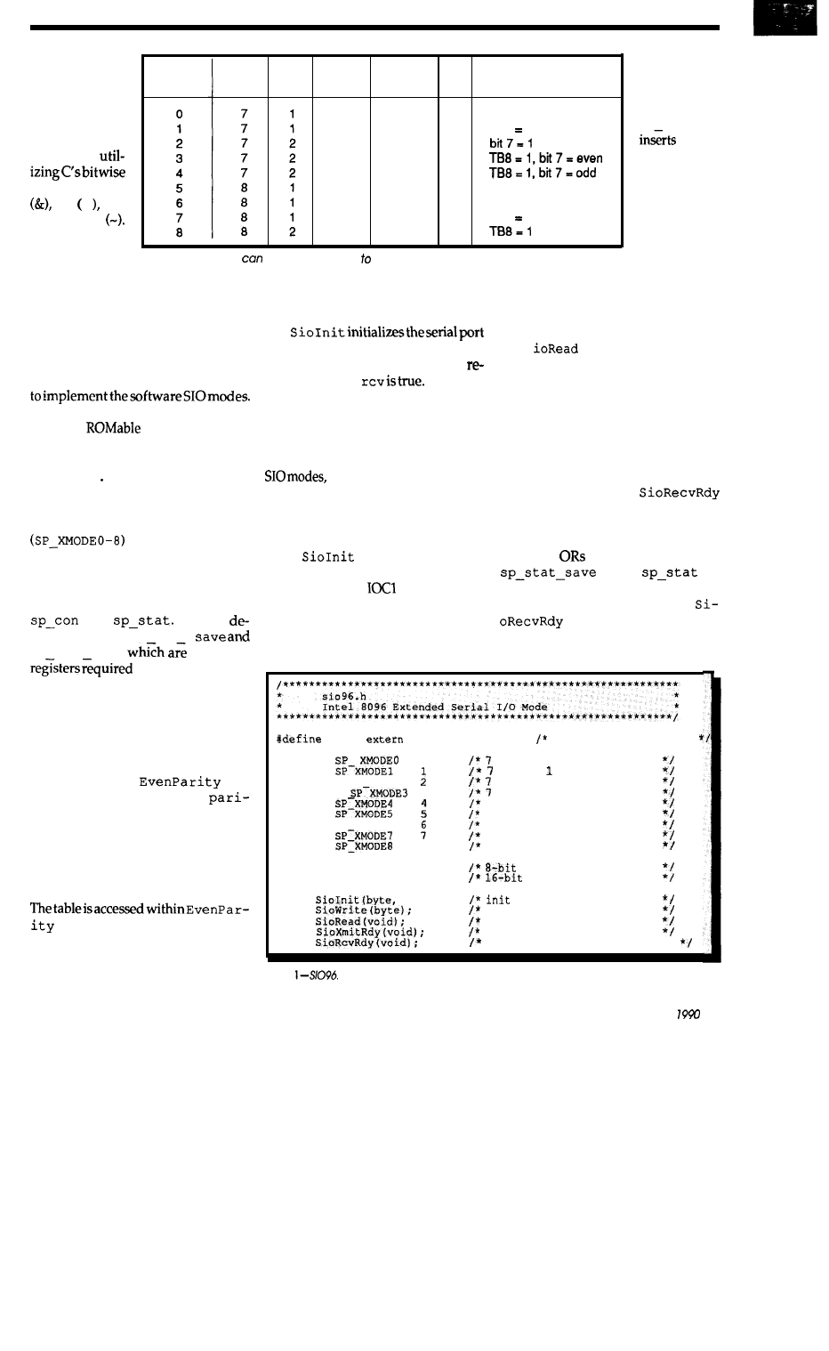
Implement-
ing the nine soft-
ware SIO modes
is a straightfor-
ward exercise in
bytewidebit ma-
nipulation
operators AND
OR I
and
complement
Special care,
however, must
be given to
working
around
Software
Mode
Data
stop
Bits
Bits
Parity
even
odd
none
even
odd
none
even
odd
none
Hardware
Mode
PEN
1
1
1
0
1
0
3
0
3
0
1
0
3
1
3
0
3
0
Comments
hardware mode 1
bit 7 odd
hardware mode 1
hardware
mode 3
TB8 odd
Figure 2-7he
8096
be programmed support nine possible framing formats, each
identified as a software mode numbered zero through eight as described in the article.
the write-only and read-only attrib-
utes of the Special Function Registers.
S1096.H AND S1096.C
Listings 1 and 2 contain the code
Compiled
fully
optimized
with Intel’s
iC96, the
code size is about
350 bytes and uses three dedicated
registers.
S IO 9 6 H is the header file to be
included
in applications using the
software SIO modes. It defines con-
stant identifiers for the nine modes
and function proto-
types for five functions constituting
low-level serial port control.
SI096. C
begins
by referencing
the external SFR registers sbuf,
and
It then
fineslocalvariablessp con
sp
stat save,
shadow
to compensate for
theread/write-only
attributesof their
counterparts. The variable
sp
mode
holds the software SIO
mode after ini-
tialization and is referenced during
serial port reads and writes to ensure
correct operation.
The function
and
its related data structures
tytableandparitymaskscomprise
the methodology used to generate
parity for seven- or eight-bit bytes.
The method chosen favors execution
speed over code size by using a look-
up table containing even parity bits.
by shifting the data value four
bits to the right to locate the appropri-
ate word which is then bit-masked
based on the lower four bits. Boolean
S i o W r i t e
conditions
the serial port
r e g i s t e r
S
P
CON and
appro-
priate parity
bits in either
the eighth or
ninth bits as
r e q u i r e d .
Equally im-
portant, it
updates the
s h a d o w
true
values returned indicate even
parity.
based on the software SIO mode
passed in mode and enables the
ceivefunctionif
Itmustbe
called prior to using the other four
functions and can be called any time
thereafter to change software SIO
modes. Since many of the software
SIO modes share common hardware
they are grouped together
to save code space. The translation
from software to hardware SIO mode
corresponds to Figure 2 which should
be referred to if the code is unclear. Fi-
nally,
initializes theshadow
registers and enables the TXD pin
through the SFR
before return-
ing.
Serial port reads and writes are
accomplished with the low-level
registersp_stat_saveindicatingthe
port is ready for writing again before
actually writing out the data.
s
is considerably simpler
than SioWrite, though its complex-
ity would be increased substantially if
parity checking were incorporated.
After updating the shadow register
sp
stat_savetoindicatereception,
it simply returns the value read from
the port with the most-significant bit
masked off for seven-bit data formats.
SioXmitRdy and
return the status of the transmit and
receive interrupt flags, respectively.
It is
important to note that each func-
tion first
the shadow register
with
to
preserve the RI and TI flag bits be-
tween reads. SioXmitRdy and
should be called prior to
SioWrite and SioRead to avoid
functions SioRead and SioWrite.
overrunning the serial port.
sfr
volatile register
special register file
#define
0
data, 1 stops, even
#define
#define
SP-XMODE2
data,
stops,
odd
# d e f i n e
3
data, 2 stops, none
data, 2 stops, even
#define
7 data, 2 stops, odd
#define
8 data, 1 stops, none
#define
SP-XMODE6
8 data, 1 stops, even
#define
8 data, 1 stops, odd
#define
8
8 data, 2 stops, none
typedef unsigned char byte;
register/scaler
typedef unsigned shortword;
register/scaler
void
byte);
extended eio port
void
extended sio mode write
byte
extended sio mode read
byte
boolean xmiter ready?
byte
boolean receives ready?
listing
His
the header fiie included in applications using the software SIO modes.
August/September
29
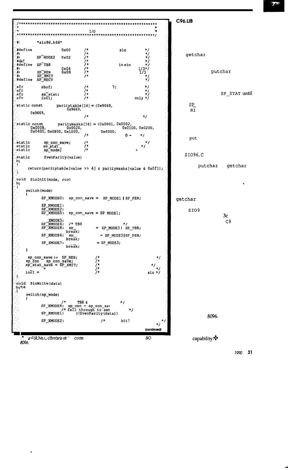
aio96.c
Intel 8096 Extended Serial
Modes
include
SP MODE0
iefine
SP-MODE1
0x01
iefine
ine
SP-MODE3
0x03
0x10
SP-PEN
iefine
iefine
iefine
0x20
0x40
byte
byte sp con;
byte
byte
8096 native
mode 0
8096 native sio mode 1
8096 native sio mode 2
8096 native sio mode 3
ninth bit
mode 3
parity enable modes
receive enable
mode
*I
transmit interupt flag
I* receiver interupt flag
register
read/write
register 17: write only
register 17: read only
register 22: write
word
0x6996, 0x6996,
0x9669, 0x6996,
0x9669, 0x6996, 0x6996, 0x9669,
0x6996, 0x9669, 0x6996, 0x6996, 0x9669);
bit set if even parity
word
0x0004,
0x0010,
0x0040, 0x0080,
0x2000,
0x8000);
masks for bits 15
byte
shadow write only reg
byte
save;
byte
shadow read only reg
extended sio mode 0 8 *I
byte
rte
value;
rte
mode, rev;
case
break:
case
case
cane
break;
case
SP
case
case
permanently set
can-save
case
eon-save
case
sp con-save
if {rev)
enable receive function
=
save for future writes
*f
initialize for writes
sp mode mode;
save for write routine
0x20;
enable TXD pin for
data;
set
fall through
ease
con save:
to odd
case
if
break;
case
data I= 0x80;
force
high for odd
break;
f*
parity/second stop bit
Figure
me
necessary to implement software
modes on
the
The C96 Library supplied with
the Intel C compiler for the 8096 con-
tains many of the standard C I/O
functionssuchasprintf,putchar,
and
which are written to
use the serial port of the microcon-
troller on a polled basis. A problem
arises when the
routine is
called the first time. Since nothing has
been transmitted, the
T
I
bit cannot be
set, thereby putting the routine in an
infinite
loop polling
TI is set. Another problem arises
when
STAT
is read since both the
TI and flags are cleared each time.
SincegetcharalsopollsSP_STATto
seewhenacharacterhasbeenreceived,
it causes T
I
tobeinadvertentlycleared
while checking for the RI bit to be set.
When
char
is called again, this
can cause the program to enter the
infinite loop described above.
can be used to correct
these bugs by rewriting the standard
functions
and
as
shown in Figure 3a and 3b.
These functions should be linked
before the standard library
C
9 6 LIB
inyourapplication. Alternatively,you
canreplacetheroutinesputcharand
in C96.
LIB
by compiling
each into a separate object file along
with
6.
c
and executing the
commands in Figure (be sure to
make a backup copy of 6.
LIB
be-
fore making any changes).
NEW MODES FOR NEW
APPLICATIONS
The 8096 (and the functionally
equivalent 8051) support hardware
serial input/output modes primarily
intended for host and multiprocessor
communications. Through the use of
demonstrated software, these modes
can be extended to provide multiple
framing formats common among
computer peripherals. In addition,
the routines discussed fix a poten-
tially fatal bug in the Intel standard C
library for the
The software is
functionally compact and when used
with embedded C applications on the
8096 provides a robust SIO communi-
cations
August/September

8031
Modules
N E W ! ! !
Control-R II
Industry Standard
803 1 CPU
128 bytes RAM 8 K of EPROM
Socket for 8 Kbytes of Static RAM
11.0592 MHz Operation
bits of parallel I/O plus
access to address, data and control
signals on standard headers.
MAX232 Serial I/O (optional)
volt single supply operation
Compact 3.50” x 4.5” size
Assembled Tested, not a kit
$64.95
each
Control-R I
Industry Standard
803 1 CPU
128 bytes RAM 8K EPROM
11.0592 MHz Operation
bits of parallel I/O
MAX232 Serial I/O (optional)
volt single supply operation
Compact 2.75” x 4.00” size
Assembled Tested, not a kit
$39.95
each
Options:
l
MAX232 I.C.
l
6264 8K SRAM
Development Software:
l
51 Software ($50.00)
Level II MSDOS cross-assembler.
Assemble 803 1 code with a PC.
l
51 Software ($100.00)
MSDOS cross-simulator. Test and
debug
Ordering Information:
Check or Money Orders accepted. All
orders add $3.00 S&H in Continental
or $6.00 for Alaska, Hawaii and Canada.
Illinois residents must add 6.25% tax.
Cottage Resources Corporation
Suite 3-672, 1405 Stevenson Drive
Springfield, Illinois 62703
(217) 529-7679
case
= s p
set TB8 high
if
bit7 even par
data I= 0x80;
break;
c a s e
if
TB8 is odd par
sp_con_save
else
sp con-save
-SP
set TB8
case _
sp
=
TB8 on in
sp stat save
clear xmit ready flag
sbiif =
write data to sio port
byte
sp stat save
clear
ready flag
SP XMODE4)
8 data bit modes only
e l s e
mask parity/stop bit 7
byte
cleared
on read
I=
byte
stat cleared on read
listing
2-continued
int
int
int
while
while
return(c):
LIB96 ADD
TO
LIB96 REPLACE PUTCHAR.OBJ,GETCHAR.OBJ IN
the
librarymaybe
and
(b) routines. The new routines may be included in the library using
librarian
commands (c).
Further Reading
Intel
Corporation.
Katz,
Ron, and Boyet, Howard. The
bedded Controller Handbook.
8096: Programming,
Santa Clara, CA: Intel Corporation,
ing, Applications. New York,
1989.
Microprocessor Training, Inc., 1986.
Intel Corporation. iC96 Compiler
John B. Design with
SantaClara,CA: Intel
crocontrollers.
New York, NY:
Corporation, 1988.
McGraw-Hill Book Company, 1988.
Alfred
was
formerly
Chief Financial
Officer of
Corporation. An
programmer and recent hardware neo-
204 Very Useful
phyte, he recently relocated to Seattle for a
205 Moderately Useful
changeoflifestyleand topursueotherinterests.
206 Not Useful
32
CIRCUIT CELLAR
INK
ONDI-The ON-line
Device Interface
Part 1
John Dybowski
ontrolling computers re-
motely via modem is coming into
vogue. There are a number of soft-
ware packages available that allow a
user at a remote site to log on, access
the command line, and exchange files
with a host computer. All require the
host to be powered up and running
special software in order to be acces-
sible. These requirements can cause
serious problems when remote con-
trol is required, so I started looking for
more reasonable, full-featured solu-
tions.
As is often the case, a better bal-
ance of features and performance can
be obtained by combining hardware
and software; what we need is an
line Device Interface: ONDI. ONDI is
a hardware device that can manage
the
key
computer
the keyboard, COM port, and com-
puter power-under remote control.
Due to the popularity of IBM PC-type
computers, this project will focus on
an interface device specifically de-
signed to work with IBM (or compat-
ible) PC/XT and AT computers (or
with a cable adapter). ONDI,
along with a Hayes-compatible mo-
dem, will allow a remote computer to
log on to the device, control power to
the computer, simulate keyboard
input, and allow direct communica-
tions to the computer. Password pro-
tection, line monitoring (for idle ter-
minals and special escape sequences),
and various other commands that can
be invoked locally or remotely will
round out the feature set that will be
discussed in detail in the next issue
when we cover the software side of
ONDI.
Building a Powerful Remote Control for Your PC
DECISIONS, DECISIONS...
First we must make some deci-
sions on implementing the hardware.
Electrically, this project will involve a
microcontroller, keyboard interface,
serial interface, power relay, miscella-
neous indicators and switches, and a
power supply. To implement
for the system, we need a
trollercapableof modest performance,
a UART, some parallel I/O, program
memory, battery-backed data mem-
ory, and a program watchdog. A rea-
sonable choice would be an Intel 8031.
Now, with the 8031 it’s always the
same old story: everyone seems to
agree that the part is a pain to use, but
it’s hard to resist the savings in parts
count that the on-chip peripherals
provide. The bottom line is, there’s a
lot of grumbling and a lot of 8031s
being sold. The main problem with
the 8031 is that, in spite of the integra-
tion of peripheral functions, many de-
signers use the part in its external
memory mode that requires more
parts and ues more I/O pins which, in
turn, generally forces the use of more
parts to restore the lost I/O.
THE GUYS IN THE BACK ROOM
Now everyone can have a per-
sonal research and development
team..
know, the guys they keep
locked away in some back room. Two
outfits in particularcome to mind that
have consistently produced what
could be considered widgets and in-
ventions. Dallas Semiconductor pro-
vides theanswer to the microcontroller
problem in the form of the
by
integrating all the requirements men-
tioned above on a 0.84” by 2.65” prefab
The DS2250 is instruction
set compatible with the Intel 8051 but
integrates on-chip many of the fea-
tures needed in most control applica-
tions: program and data memory, lith-
ium backup power for memory,
watchdog timer, and perhaps most
important, an embedded serial pro-
gram loader.
One of the most notable features
of the DS2250 is its close resemblance
to the 8051, quirks and all. Perhaps it
would have been a good idea to en-
hance the instruction set or to provide
an extra data pointer, but Dallas ex-
hibited tremendous restraint in ren-
dering the part. This could be a valu-
able lesson: it’s all too easy to get
buried in myriad features of dubious
usefulness. The density the DS2250
affords sets the tone for a compact
circuit design which is further en-
hanced with the aid of a few parts
from Maxim. The MAX612 integrated
AC-to-DC power converter and
MAX233 single-chip dual 5-volt-only
RS-232 transceiver. We’ll throw in
some mundane so we don’t have too
much fun and tie everything together
with some HC logic. Now let’s look at
the hardware.
THE HARDWARE
The controller is
an
DS2250
with of embedded RAM. The
MHz version is the least expensive
and provides adequate performance
for this project. The crystal frequency
of 5.5296 MHz is used because the
DS2250 automatically determines the
34
CIRCUIT CELLAR INK
baud rate to use for communications
when in program load mode. Since
5.5296 MHz is half the standard fre-
quency of 11.0592 MHz, the controller
can operate at standard baud rates
using the program load facility at the
host computer. The power-on reset is
implemented within the DS2250, so
no external components are required
for this function.
Linepowerat
brought
directly onto the main board and is
stepped down (and isolated) to 8
VRMS, rectified, and regulated to
VDC. A Maxim MAX612 power
vertorprovides rectificationand regu-
lation, keeping the power supply
component count low. The ‘612 con-
tains a full-wave bridge rectifier, an
zener diode,and a 5-VDC series
regulator in an B-pin DIP package.
The addition of a Signal
VRMS transformer, a
filter
capacitor, and a peak-input
limiting resistor provides a
+5-V,
power supply that will op-
erate at a line voltage of from 80 to 160
VRMS. There
is
no
power switch-the
intent is to have power present to the
device at all times.
Computer power
iscontrolled via
an optically isolated solid-state relay
The power SSR is a IO-amp
VAC unit with built-in snubber. A
series resistor is connected between 5
V and the positive control terminal in
order to limit control current to the
minimum level required for reliable
operation. Since the required control
current is kept low, the return control
terminal is driven directly from PO.4
of the DS2250.
The mode switch is a three-posi-
tion, single-pole/double-throw
toggle-type with center off. The com-
mon is tied to ground with the
switched contacts connected to PO.6
and P3.5. Note that the switch body is
tied to earth ground to divert any
static discharges from the unbuffered
switch connections to the DS2250.
Four
are used to indicate
status information. These are HLMP
4700 low-current types that operate at
2
Three of the
are under
software control and are driven di-
rectly by
and PO.2 of the
DS2250. The fourth LED denotes pro-
gram load mode and is connected
directly to the program load switch.
The program load switch is a
triple-pole/single-throw switch used
to place the DS2250 into the program
con figuration switches and lights.
snows
tor two serial ports, keyboard input and output ports, and a
of
August/September 1990 35
SIGNAL
AC1
AC2
“ S E T - - J _
SENSE +
AC
3
SENSE
8
S t a t s
L I N E
C o n t r o l
Figure
2-A MAX6 12 is used to regulate 5 volts from the power line, while the computer’s
power Is switched using a solid-state relay.
load mode and energize the power
SSR. The three poles of the switch are
connected as follows: 5 volts isbrought
out to the
RST pin and to the
anode of the load LED. Ground is
brought to
and an independ-
ent ground connection is brought out
to the return control terminal of the
power SSR. The DS2250 enters pro-
gram load mode when
is
brought low and RST is simultane-
ously brought high. This mode is
indicated by the load LED being lit. It
is assumed that program loading will
be performed from the host computer,
therefore the power SSR is energized
when the switch is placed into the
load mode, overriding the power SSR
control pin from the DS2250.
KEYBOARD INTERFACE
The IBM keyboard electrical in-
terface consists of a clock and a data
signal. The procedure used to trans-
mit a bit is to set the data line to the
appropriate level, then assert the clock
low, then bring it high again. The data
is valid from before the falling edge to
after the rising edge of the clock. The
bit transmission is the same for both
the XT- and AT-style keyboards. The
number of bits per scan code, method
of indicating make/break codes, idle
signal states, and protocol differ de-
pending on the keyboard style.
Data from the keyboard normally
passes transparently through to the
computer, but the DS2250 can also
seize control of the keyboard port,
switch out the keyboard, and supply
its own simulated keyboard data
stream to the computer. Switching is
accomplished with a DG302 dual
double-pole/single-throw solid-state
analog switch. Each switch has an
associated control line. The seize sig-
nal, KSO, is driven from P3.4 and is
connected to the control line of one of
the
control lines, and to the
other control line through a
transistor, which functions as an
verter. Wired in this way, the
functions as a dual double-pole/
double-throw switch. The analog
switch is required since the keyboard
communication protocol is defined as
bidirectional; the switch allows sig-
nals to pass in either direction. The
DS2250 drives the keyboard clock and
data signals with two gates of a
tristate buffer arranged to
function as an open-drain device.
The keyboard clock and data at
the computer interface are received
and are presented to INTO\ and P1.5
respectively. The receive section is set
up to disable reception of clock and
data while the DS2250 is transmitting
its simulated keyboard data stream;
this is intended to simplify the inter-
rupt-driven receive routine. The clock
and data lines are tied to ground at the
computer interface via
resistors
in case the device is operated without
its keyboard interface connected (to
prevent float conditions). The
putef s 5-V logic supply is present on
the keyboard interface and is moni-
tored by the DS2250 via a
emitter transistorarrangementonP0.7
to determine when the computer is ac-
tually powered up.
SERIAL INTERFACE
The serial interface is the heart of
the system and contains the drivers
DG302
d e f a u l t
f r o m P C ’ S
C L K
C o n t r o l
f r o m M o d e m ’ s
S e r i a l P o r t
X M I T R E C
C o n t r o l
XMIT
REC
d e f a u l t
. . . . . . . . . . . . . . . . . . . . .
J
CLK
t o P C ’ S
t o P C ’ S
K e y b o a r d C o n n e c t o r
S e r i a l P o r t
d e f a u l t
gure
J-Redrawing the
in
the form of switches helps clarify their operation.
36
CIRCUIT CELLAR
THE DS2250
The
is
a CMOS
microcontroller that emulates the functions of an
8051. The program/data memory space is implemented using nonvolatile CMOS
static
that resides on its own internal embedded memory bus.
leaves all
chip parallel I/O available for use as I/O. Nonvolatile operation is accomplished
an embedded lithium power source that will maintain the nonvolatile areas of the
for 10 years in the absence of primary power. Initial loading of the application
software into the
is possible from either a parallel or serial interface to the host
system. This function allows initialization of the nonvolatile areas of the device
including program/data RAM and the configuration parameters. The
incor-
porates control
functions
which provide crashproof operation when system power is
momentarily disrupted or removed. These functions include the power fail warning
interrupt, automatic power down, and power on restart. Regardless of the duration of
the power outage, the
has the ability to resume execution when power is
restored as if the power failure had not occurred at all.
REGISTERS
All CPU registers are mapped as special function registers
and are
identical in number and function to those present in the 8051. The power control
register is in the same location as in the 8051. All of the bits in this register
remain unchanged in the
implementation with the Following exceptions: the
(PCON.3) and GFO (PCON.2) flags have been changed to enable the power fail
interrupt and enable the watchdog timer reset mask bits, respectively. The previously
unused PCON.5 bit has been assigned as the power fail
flag which may be polled
by the application program to test for a power fail condition.
MCON register is
used to define the total range of memory in the embedded RAM and the respective
amounts of program and data memory within the embedded RAM. The timed access
register interfaces to logic that is used to prevent
to key internal resources
in the event of errant program execution. These resources include the partition address
in the MCON register and the watchdog timer control bits in the PCON register.
EMBEDDED PROGRAM/DATA RAM
Current versions of the
incorporate from
to 64K of RAM on the
embedded memory bus. On-chip logic allows this memory to be partitioned during
initial loading of application software as program memory or data memory. This must
be done in order for the
to begin execution of the application software from the
space in which it has been loaded. The
preserves the Harvard memory
of the 8051, in which there are separate areas for program and data memory.
The
does not permit the overlapping or combining of program and data
memory; the partition address is the point at which program memory ends and data
memory begins. At first this may seem like a disadvantage since it would appear that
unnecessary
must be incurred in accessing the separate regions. Actually
this
is an important safety feature. Since the
executable
program residesin RAM, errant
program execution could corrupt the program itself if it were possible to write to this
region. The
enforces the separation of address spaces; therefore, since no 8051
instruction exists for writing to program memory, it is impossible for the
to
modify its program while executing (unless the partition address becomes reset).
PARALLEL I/O
Four
provide access for the four parallel I/O port latches (PO,
A
total of 32 bits of parallel I/O is available through these I/O ports. All are available
when embedded RAM is used for program and data memory.
TIMED ACCESS LOGIC
Timed access logic is used to protect against
changes to program
RAM and the configuration parameters in the event of a loss of software control. The
protected configuration area includes
the
partition address bits in the MCON register,
the watchdog timer enable bit, stop mode bit, and power-on-reset bit in the PCON
register. These protected bits may only be written through the execution of two con-
secutive write operations within four machine cycles of each other to the timed access
register. The first write operation must be with a value of
and the
second
with
a value of
55H. When this
sequence is performed, write access is allowed to the
protected bits, which must be written within four
of the double write
sequence to the timed access register.
SAVE Development
and Debugging Time
of Embedded
Microprocessor Systems!
l
INTROL-C
Cross-Compilers
l
INTROL-Mcdula-2
Compilers
l
INTROL Relocating Macro
Cross-Assemblers
COMPILER PACKAGES INCLUDE:
Compiler
l
Assembler
l
Linker
l
library, including
a multi-tasking executive
l
Support utilities
l
Full
maintenance
TARGETS SUPPORTED:
l
.
l
AVAILABLE FOR FOLLOWING
HOSTS: VAX and
Apollo; SUN; Hewlett-Packard;
Macintosh; Gould
Node; IBM-PC, XT, AT, and
compatibles
INTROL CROSS-DMLOPMENT
SYSTEMS are proven, accepted
and will
time, money,
and effort with your develop
ment. All INTROL products are
backed by full,
meaningful,
technical support.
CALL or WRITE
for facts NOW!
C O R P O R A T I O N
Howard Avenue
Milwaukee, WI 53228
Quality Software Since 1979
August/September
and receivers as well as the
switching circuitry. RS-232 data is re-
ceived using a MAX233 line driver/
receiver and all data manipulations
are performed on the CMOS HC-level
signals. Data received from either the
modem or the computer is routed to
the DS2250 via a multiplexer con-
structed from a 74HCO0. The routing
is determined by the signal SS2 driven
by P1.2. When this signal is at a logic 1,
the
receives the computer
transmission; when SS2 is a 0, the
receives the
sion. Outgoing data is presented to
the
dual 4-to-1 multiplexer.
The computer-bound mux is
by the modem transmit, the DS2250
transmit, and a marking signal. The
modem mux’s inputs are from the
computer transmit, DS2250 transmit,
and marking signal. The SSO and
signals, driven by
and P1.l re-
spectively, determine which signals
are connected to the computer and
modem receive lines. Table 1 contains
a summary of the binary routing ar-
rangement.
All the main RS-232 signal lines
with the exception of DTR, receive,
and transmit are passed directly from
the modem port to the computer port.
DTR is connected to the 10-V output
of the MAX233 through a
resistor
and is always on. Also, theDS2250 has
the capability of monitoring the more
important RS-232 lines-DSR and
particularly DCD. The DS2250 receives
the signals using two
com-
mon-emitter transistors and samples
them on P3.6
and P3.7
The diode clamps on the base leads
limit the negative swing from the
232 level signals.
In the design of embedded sys-
tems, the states that the system signals
assume at power-up are an important
consideration, particularly in the case
of malfunctioning or nanfunctioning
equipment. In this design, the default
larly important because the
is
essentially reset when it is in program
load mode. The reset state criteria is
defined as follows:
38
CIRCUIT CELLAR INK
WATCHDOG
When user software is executing, the watchdog timer can be used to restart the
processor in the event of errant program execution. When the watchdog timer is
enabled, it will eventually timeout after a fixed number of clock cycles unless it is reset
by the application software. An internal reset to the CPU is generated if the timeout
condition is ever reached.
SERIAL PROGRAM LOADER
The
is placed in its program load configuration by simultaneously
applying a logic 1 to the
pin and forcing
to a logic 0 level. Immediately
following this the
will look for a serial ASCII carriage return (ODH) character
received at
or 300 bps over the serial port. A standard
is required in order for communications to take place at standard baud rate
frequencies. (A
crystal
also work since it is half the standard
frequency and the
be able to recognize the standard baud rates up to 4800
bps.) A software utility program for an IBM PC is available to configure and load the
without detailed knowledge of the operation of the
serial load
command line syntax.
Important safety tip: Leave
and M.6 open or pulled up during serial pro-
gramming. Failure to do this results in parallel load operation.
DS2250 transmit is routed to the
computer. Computer transmit is
routed to the DS2250. Keyboard is
passed directly through to the com-
puter. Front-panel
Power
SSR is deenergized. When in program
load mode, the load switch will turn
on the load LED and energize the
power SSR.
That’s the hardware, with a little
help from the guys in the back
room.. .and ONDI. We now have a
programmable interface device with
some hooks that can be put to use in
various situations. By virtue of the
keyboard emulation and power con-
trol capabilities, we can devise appli-
cations where ONDI exercises control
over the host computer. With some
PC software, this presents the oppor-
tunity for distributing the processing
burden. Although we can consider
some interesting uses for the interface
device, for the time being we’ll stick
with remote computer control. Next
time we’ll explore the system soft-
ware for a remote control application,
program downloading, and go into a
little detail on keyboard protocols.
Unfortunately, things go downhill
from here. When it comes to software,
we can’t call on the guys in the back
room-we are the guys in the back
room.
John Dybowski has been involved in thedesign
and manufacture of hardwareand software
for
industrialdatacollectionandcommunications
equipment. His crowning achievements are
his daughter Ondi and his son John.
SOURCES
Dallas Semiconductor Corp.
4350
Pkwy South
Dallas, ‘IX 75244-3219
(214) 450-0400
Maxim Integrated Products, Inc.
120 San
Dr.
Sunnyvale, CA 94086
(408) 737-7600
IRS
207 Very Useful
208 Moderately Useful
209 Not Useful
sso
Computer Receive
Modem Receive
0
0
Modem Transmit
0
1
DS2250 Trahsmit
1
0
Marking Signal
1
1
Transmit
Computer Transmit
Computer Transmit
DS2250 Transmit
Marking Signal
‘able 1 -The
ond
lines control
interconnections
the serial
Part 2
David
Building MITEE Mouse
The
for a Maze-Running Rodent
n Part of this article described
the hardware for building a micro-
mouse. Using MITEE Mouse III as an ex-
ample, I described what type of sys-
tems are required and how they might
be implemented. In this second ar-
ticle, I hope to breathe life into the
hardware by describing the ideas
behind the mouse software.
MAZE SOLVER
(the most optimistic assumption). At towardthegoalagain,italwaysknows
every square that has any unknown the true wall
at least
One aspect of building a micro- walls surrounding it, the mouse stops where it started, and is therefore able
mouse which attracts many people is and updates its maze map with the to advance at least one square.
the
maze
solver. This is not as difficult true information. When it sets off
Each time MITEE Mouse III sets
as is often perceived,
however. The algo-
rithm described here,
which is variously
known as Bellman’s al-
gorithm or the flooding
algorithm, will find the
optimal path through a
maze once the configu-
ration (walls and open-
ings) is known. The ini-
tial problem, of course,
is that the walls and
openingsareunknown.
What is known, how-
ever, is that the maze is
a 16 x 16 square array,
MITEE Mouse III starts
by building a map of
the maze in its mem-
ory. Initially all the
walls in the maze are
marked as unknown. It
thensetsoff toward the
goal, assuming the un-
known walls are open
03
13
23
33
4
0
0 2 - - - -
6
5
- - - - -
01
7
3;
1
31
2
Figure 1 -A sample 4 x 4 maze.
off toward the goal, it
runs the maze solver.
Figure 1 showsasample
4 x 4 maze with the start
in square 00 and the fin-
ish in square 33. For the
initial example, the
shortest path is consid-
ered the optimal path.
The objective of the
algorithm is to fill each
themazewith
a number representing
the minimum distance
from that square,
through
to the
goal. This is accom-
plished in a series of
iterations. On each it-
eration, all the squares
of a given distance are
filled in. Since the next
iteration will always fill
in squares adjacent to
the squares filled in on
the last iteration, these
40
CELLAR INK
squares
are
called tails and
maintained in a
list.
The solver
starts by num-
bering the goal
square with 0.
On the first itera-
tion, square 32 is
given a number
of 1 and put in
the list of tails. It
is the only
square which is
adjacent to the
goal square and
not separated
fromitbyawall.
LEFT WHEEL
POSITION
LEFT
CONTROL
RIGHT
CONTROL
RIGHT
POSITION
Figure
2-Separate controllers are used for
combined to drive the motors.
forward and rotational movements, with the
eration, square 32 is retrieved from
the tail list and analyzed. Square 22
and square 31 are adjacent to square
32 and not separated by a wall, so they
are given a number of 2 and replace
the previous entry in the tail list. On
the third iteration, square 23, square
21, and square 30 are given a number
of 3 and put in the tail list. The fourth
iteration deletes the tail at square 21
since
no unnumbered squares
adjacent to it that are not separated by
walls. It also numbers square 13 and
square 20 with a 4. On the sixth itera-
tion, the two tails that meet at square
11 arecombined into a single tail. This
tail is then deleted during the seventh
iteration because there are no unnum-
bered squares adjacent to it. The
eighth
iteration numbers square 00, the start
square, which terminates the num-
bering process. The optimal path is
now found by starting at the start
square and proceeding to the square
with the next lower number until the
goal square is reached.
The maze solver always gives the
best path based on the assumptions.
When the optimal path does not take
the mouse through any unknown
walls, there are no more assumptions
that need to be verified. The maze is
now solved. There may be unknown
walls left in the maze, and indeed
finding the best path without fully
mapping the maze is always a secon-
dary goal, but they will not influence
the path selected by the mouse.
This algorithm can be extended to
compute the fastest path instead of
the shortest path. This is done by fill-
ing the squares with the time to the
goal instead of the distance to the goal.
Many mice are able to accelerate on a
long straight section so that the total
time for N squares in a line is much
less than N times the time for one
square. This requires keeping track of
the number of squares in a straight
brake it. Good
control of each
wheel is clearly
required to pro-
vide good overall
control of the
mouse in the
maze.
M I T E E
Mouse III uses DC
mental encoders
to drive each
wheel through a
spur gear. The en-
coder measures
the position of the
motor shaft. Soft-
ware in the mouse
compares the ac-
tual position of the motor with the
desired position, and computes an
error. This error is used to drive the
DC motor. Unfortunately the motions
of the two wheels are not independent
since they are connected together by
thechassisofthemouse.Tocreatetwo
independent control signals, the mo-
tion is resolved into two modes: for-
ward motion, where both wheels turn
in the same direction; and rotational
gure J-Each
of the motor control loops can be represented for analysis purposes by a
block diagram.
and knowing the incremental time for
each additional square when filling in
the time. In order to demonstrate the
fastest-path capability of a mouse,
most contest maze designs include
straight sections that are several
squares longer than the shortest path.
SERVO LOOP
The movement of MITEE Mouse
III is controlled through two drive
wheels. Differences in speed of the
twowheelsareusedtosteerthemouse,
and changes in average speed of the
two wheels are used to accelerate and
motion,
where the wheels turn in
opposite directions. As shown in Fig-
ure 2 separate controllers are used for
theforwardandrotationalmovements
with the outputs combined to drive
the motors.
Each of the control loops can be
represented by the block diagram
shown in Figure 3. The filter
is a
lead-lag filter used to stabilize the
feedback loop. The
(zero-order
hold) is a time delay, modeling the
fact that the control signal to the mo-
tor is only updated periodically. is
the gain of the power amplifier driv-
ing the motor. The dynamics of the
August/September 1990
2764-27256
ROM EMULATOR
Appears as EPROM to
target sys
l
Connects
to PC
parallel
l
Plugs into target ROM socket and connects to PC
parallel port via modular telephone cable
l
Accepts x 8 or 32K x 8 SRAM or NV SRAM
l
Reset output restarts target after downloading
l
Uses HC/HCT logic for CMOS TTL compatibility
l
Loads Intel Hex, Motorola S, hex, and binary files
l
Command line software can be run from batch
files for automatic downloading after assembly
$ 9 9
$119
$139
8
8
8051
FAMILYASSEMBLER
l
Works on all 8051 derivatives
l
Supports standard Intel syntax
l
Allows local labels and include files
l
Labels may be up to 32 characters
. Generates assembly
Outputs Intel Hex
Quick
l
Dependable
l
Clean Operation
DEVELOPMENT TOOLS
Programmer
Board
Programs
“Mini-ICE” for the
external EPROM
Handles EPROM, key, and
socket for program memory.
security bits. Loads Intel Hex,
Very useful when
ASCII hex, and binary files
ROM emulator
Programmer-DIP
9299
Board
Board and
$338
Programmer PLCC
$929
(Includes PLCC
motor driving the load of the mouse
are contained in
This term will
be different for the forward and rota-
tional controllers. The term is due
to the conversion from wheel speed to
its integral, wheel position. is the
gain of the shaft encoder.
To analyze
is help-
ful to realize that the drive motors
generate a torque, and this torque acts
on an inertia. It is therefore conven-
ient to convert the load on the mouse
motors to an equivalent inertia. is
the inertia seen by the forward con-
troller and is based on the mass of the
mouse. is the inertia seen by the
rotational controller and is due to the
reflected moment of inertia of the
mouse.
-
-
where:
=
mass of the mouse
= moment of inertia of the
mouse
=
radius of the drive wheel
= radius of the mouse (half
the distance between the
drive wheels)
= gear ratio from motor to
drive wheel
The torque supplied by the mo-
tors is proportional to the motor cur-
rent which in turn comes from the
power amplifier through the motor
resistance. This torque acts on the
motor inertia, as well as the reflected
inertia of the load, to create two time
constants, one for each mode.
Jr)
where:
= inertia of the motor armature
= torque constant of the motor
R =
resistance of the motor
In addition to themechanical time
constants, there is also an electrical
time constant due to the inductance
and resistance of the motor winding.
This is combined with the back EMF
of the motor to provide the overall
transfer function.
=
+ 1)
=
where:
= back EMF of the motor
= electrical time constant of
the motor
The previously mentioned
lag filter
was added to the feed-
back loop to improve its bandwidth
and stability. The design of the filter
was done with a computer-aided
design program called
In
addition to calculating the pole and
zero placements of the filter, this pro-
gram also converts the
entation. The discrete-time implem-
entation accounts for the fact that the
control signal to the motor is only
updated periodically. Each new con-
trol output to the motor is based on a
new error measurement, the error
measurement of the previous sample,
and the control output of the previous
sample.
new output = K, x new error
x old error
+ x old output
The constants
and are
calculated by
from the
continuous-time filter parametersand
the sampling rate.
The 78312 processor used on
MITEE Mouse Ill has a
multiply
instruction but unfortunately it is
unsigned. The
the
product
must
be determined by software. Only the
error terms are signed, however; the
constants are all positive. This allows
some savings in code size and execu-
tion time over a full signed multiply
routine. MITEE Mouse Ill uses a
sampling rate and requires ap-
proximately 86 to execute the
bly not necessary, in-line coding in-
stead of subroutines is used to mini-
mize the execution time.
The servo loop is very good at
correcting errors in wheel position,
but it can only do this after they occur.
Certain errors however, are
Reader
Service
42
CELL4 R INK
able and can be anticipated. To correct
them, a feed-forward term is added
into the voltage driving the motor.
Feed-forward terms for static loss such
as bearing and brush losses, as well as
velocity and acceleration were imple-
mented.
The gain of the power amplifier
depends on the battery voltage.
inga run through the maze the battery
voltage may vary from 12 to 9 volts. To
minimize the effect this has on the
gain of the feedback loop, as well as
the feed-forward compensation, the
battery voltage is continuously meas-
ured. This information is then used to
hold the overall gain of the amplifier
constant. [Editor’s Note:
Software
for
this project is availableon the Circuit Cel-
lar BBS and on Software
On
Disk
ordering
PROFILE GENERATOR
After the servo loop is completed
and the wheels can be moved to a
commanded position, there remains
the task of coming up with a series of
positions which fulfills the other re-
quirements of the mouse. The soft-
ware which does this is called the
profile generator. There are two main
types of maneuvers the mouse must
perform: straight runs and turns. In
general, the mouse will try to do both
of these in the least amount of time.
The major limitation to the speed of
the mouse seems to be wheel traction.
For a specific value of wheel traction,
the forces used to accelerate, brake,
and turn the mouse must be corre-
spondingly limited. Because of this,
we try to optimize the performance of
the mouse for a given force.
The force,
F
which the motors,
wheels, and
the tires of the
mouse can apply parallel to the floor
of the maze to accelerate and move the
mouse, is
shown below.
where:
coefficient of friction of tires
= acceleration due to gravity
=
acceleration of the mouse
The maximum acceleration,
A,
which the mouse can achieve is lim-
ited by the coefficient of friction of the
tires and does not depend on the mass
of the mouse. This assumes that the
INITIAL VELOCITY
TIME
Figure 4-A
typical velocity profile along a straightaway is made up of five parameters:
and final velocities, and maximum acceleration.
and deceleration.
Introducing
the
video capture and image
processing library
Victor is a library of functions for C
that simplifies development of scientific
imaging, quality control, security, and image
database software. Victor gives you device
control, image processing, display, and TIFF/
PCX file handling routines.
software
can have featuressuch as:
live video on VGA, resize and zoom, display
multiple images with text and graphics. Image
processing functions include brightness, con-
trast, matrixconvolution filters: sharpen, out-
line, etc, linearization, equalization, math and
logic, overlay, resize, flip, invert, mirror. Size/
number of images limited only by memory.
Display on EGA/VGA up to
And, to get you up and running quickly, we’ve
included our popular Zip Image Processing
software for rapid testing and prototyping of
image processing and display functions.
Victor supports Microsoft C,
all for only $195.
Victor and Zip support
and
other popular video digitizers.
NEW! ZIP Colorkit, the
software that allows any
gray scale digitizer to create
photographic quality
color images.
It’s easy to produce stunning color imageswith
the ZIP
--capture three images with a
gray scalevideo digitizer using red, green, and
blue filters and save the images.
loads
the image
and uses a unique optimizing
algorithm to calculate the optimum color
image. Supports PIW, PIF, PCX, TIFF, GIF,
and TGA file formats. ZIP COLORKIT, $75.
VICTOR LIBRARY
includes
FREE
ZIP Image Processing . . . . . . . . . . . . $195
VICTOR LIBRARY
with
video
frame grabber . . . . . . . . . . . . . . . . . . $349
ZIP
. . . . . . . . . . . . . . . . . . . . . . . .
$75
Call
(314) 962-7833
to order
VISA/MC/COD
CATENARY SYSTEMS
470
BELLEVIEW
ST LOUIS MO 63119
(314)
962-7833
August/September 1990
43
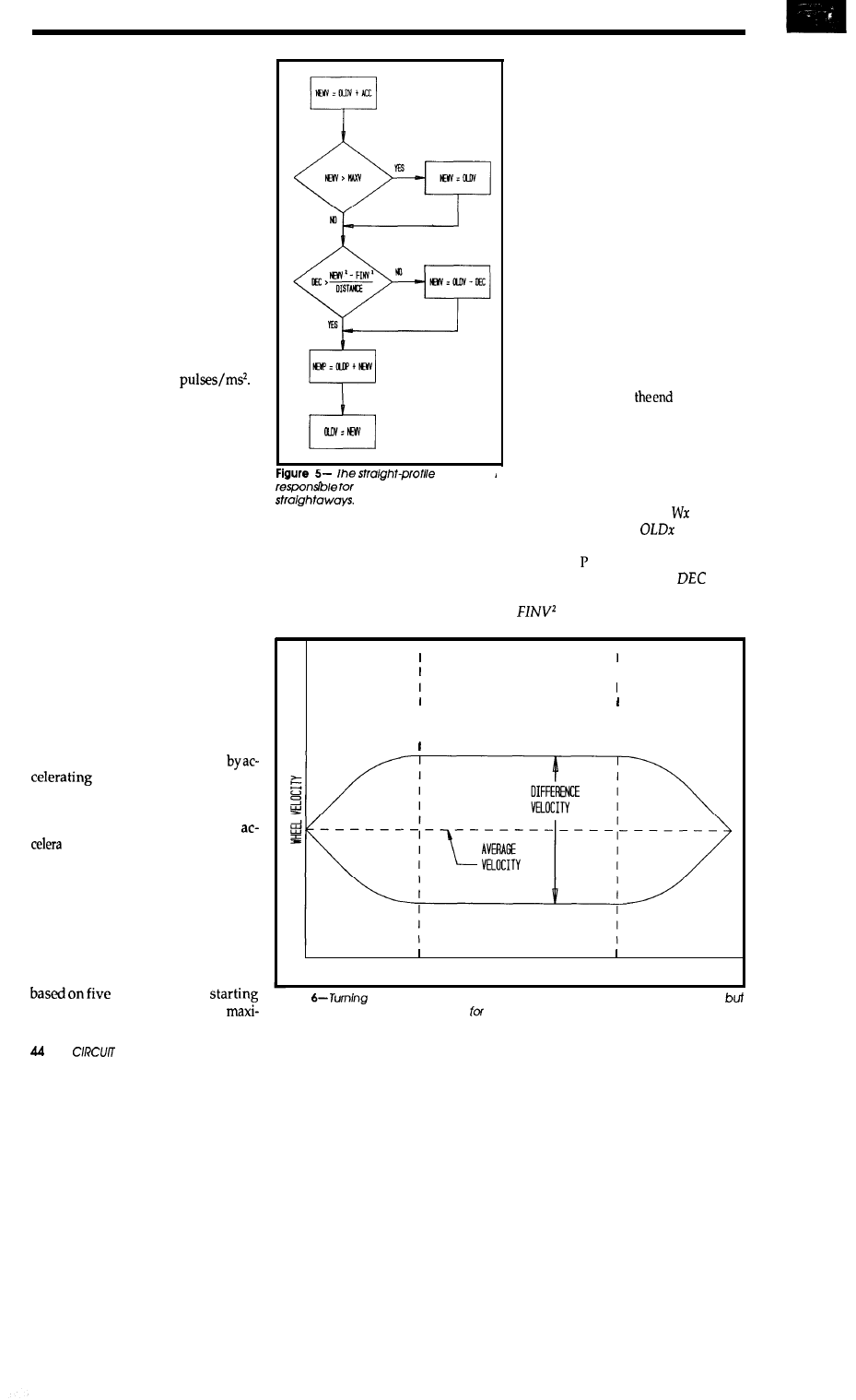
entire weight of the mouse is distrib-
uted on the wheels that are providing
the acceleration. If part of the weight
is on a passive wheel such as a caster,
the maximum acceleration will be
reduced accordingly.
To make life easy for MITEE
Mouse III while it is running through
the maze, it uses a system of units
which are more natural for it than
meters or seconds. The unit of dis-
tance is the pulse and corresponds to
the distance the mouse must travel to
register one pulse on the shaft en-
coder. The unit of time is 1 ms because
that is the time between processor
interrupts. Accordingly, one square is
4176 pulses, a 90” turn in place is 1260
pulses, velocity is
measured
in
pulses/
ms, and acceleration in
The motion control system of the
mouse is concerned with three differ-
ent quantities: position; itsderivative,
velocity; and its derivative, accelera-
tion. Because the velocity is in the
middle and the position or accelera-
tion can be computed from the veloc-
ity with only one operation, the pro-
file generator computes velocity pro-
files. Of course, the velocity profile
must have a slope or derivative con-
sistent with the desired acceleration,
and the integral must be consistent
with the desired position.
STRAIGHT PATHS
When traveling in a straight line,
the maximum available force can be
used to accelerate or brake the mouse.
If the mouse starts and ends the
straight with equal velocity, it can
cover the distance in the least amount
of time (for a given acceleration)
for half the distance and
decelerating for the remaining dis-
tance. If it is moving at different ve-
locities at the start and finish, the
tion and deceleration periods are
not equal, but the mouse will always
be accelerating or braking. For some
types of straights such as long diago-
nals, it may be desirable to limit the
maximum velocity, not because that is
the fastest way to travel, but because it
is the safest. Thus the straight-profile
generator creates a velocity profile
real time. This requirement comes
about because the mouse continually
updates its current position based on
signals from its sensors. At one in-
stant of time it may think that it still
has 20 cm to go before the end of the
straight, but the sensors may see an
opening in
a
wall signaling that it only
has 18 cm to go. If the mouse was
already decelerating at the maximum
rate based on 20 cm remaining dis-
tance, it has a problem. If it continues
to decelerate at the current rate, it will
reach the end with too high a final
velocity. If it tries to brake harder to
reach the final velocity, it will exceed
the
maximum
deceleration acceptable
for its wheel traction and the wheel
will begin to skid. MITEE Mouse III is
programmed to brake harder to avoid
entering the turn at
of a straight
with too high a velocity. If, however,
it gets to the start of the turn and the
velocity is still too high, it tries to go
through the turn at the higher speed.
generator
is
controlling
me moron on
mum velocity, maximum deceleration,
and final velocity. A typical velocity
profile is shown in Figure 4.
One important feature to have in
the straight-profile generator is the
ability to change the total distance in
Figure 5 shows a flow chart of the
straight-profile generator. Each time
through the program, NE variables
are calculated from
ones. Vari-
ables ending in V are velocities, those
ending in are positions. ACC is the
target acceleration, and
is the
target deceleration.
The variable
is the final velocity squared
MCREASING RADIUS
I
CONSTANT RADIUS
INCREASING RAOIUS
I
I
I
I
I
TIME
Parameters:
velocity, maximumacceleration,
Figure
corners is as
simple as
running the motors
at different
speeds,
knowing
the speed
differential to use
a particular corner can be tricky.
CELLAR INK
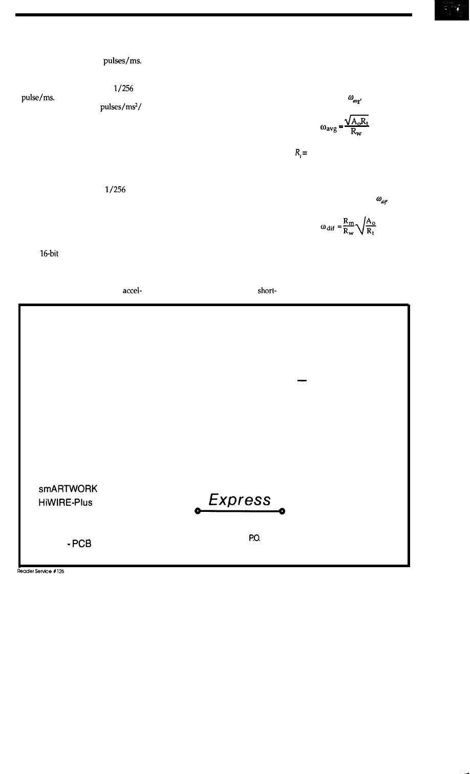
and is precalculated at the start of
every straight so that only
NEW
must be calculated every millisecond.
The velocity is stored in
This
is too coarse, however, so an
extra
byte is used to the right of the decimal
point, allowing resolution to
of
a
The acceleration and de-
celeration is specified as
256. This allows the new velocity to be
calculated by simply adding the accel-
eration to the old velocity. The new
position is calculated from the old
position by
simply adding
the new ve-
locity to it. The acceleration is stored
in one byte, the velocity in two, and
the position in three. Although the
position is calculated to
of a
pulse, only whole numbers of pulses
are sent to the servo. The fractions are
accumulated until they round off to a
whole pulse. Because the profile gen-
erator only requires one unsigned
multiplication and division, and
mostly
addition, subtraction, or
comparison operations, it is efficient
and runs in a very short time.
The straight-profile generator has
information on the speed and
eration of the mouse and therefore est time, it is necessary to keep the
generates feed-forward information forces on the tires at the maximum
that is later used by the motor control allowable value at all times. If the
routines. As mentioned before, the mouse were to travel at a constant
feed-forward terms in the control sig- speed around a constant radius turn,
nificantly decrease the error in the the only forces on the tires would be
wheel position without increasing the due to centrifugal forces. The average
gain or bandwidth of the feedback
loop.
angular velocity,
of the wheels
around such a turn would be:
TURNS
There are two types of turns.
During the search phase, the mouse
turns in place. This is a very simple
type of turn, and the profile genera-
tion is similar to a straight, except one
wheel rotates forward and the other
backward. The acceleration and de-
celeration intervals are equal, the ini-
tial and final velocities are zero, and
the distance is always fixed.
To maximize the speed through
the maze, however, it is desirable to
avoid starting and stopping every
straight from zero velocity. Also a
smooth and continuous turn will re-
quire less time than a turn in place. As
with the straight, to turn in the
where:
radius of turn
The inside wheel would turn at
one constant speed and the outside
wheel at a higher constant speed. The
difference in wheel speed,
would
be:
One minor difficulty is that the
mousecomesintoatumfromastraight
where both wheels are at the same
speed, but during the turn the wheels
rotate at different speeds. A step
change in speed, in this case a step
EXPRESS CIRCUITS
MANUFACTURERS OF PROTOTYPE PRINTED CIRCUITS FROM YOUR CAD DESIGNS
TURN AROUND TIMES AVAILABLE FROM 24 HRS
2 WEEKS
Special Support For:
l
TANGO. PCB
l
TANGO SERIES II
l
TANGO PLUS
l
PROTEL AUTOTRAX
l
PROTEL EASYTRAX
l
l
l
EE DESIGNER I
l
EE DESIGNER III
l
PADS
l
OTHER PACKAGES ARE
NOW BEING ADDED
l
FULL TIME MODEM
l
GERBER PHOTO PLOTTING
Circuits
314
Cothren St.,
Box 58
Wilkesboro, NC 28697
Quotes:
l-800-426-5396
Phone: (919) 667-2100
Fax: (919) 667-0487
August/September 1990 45
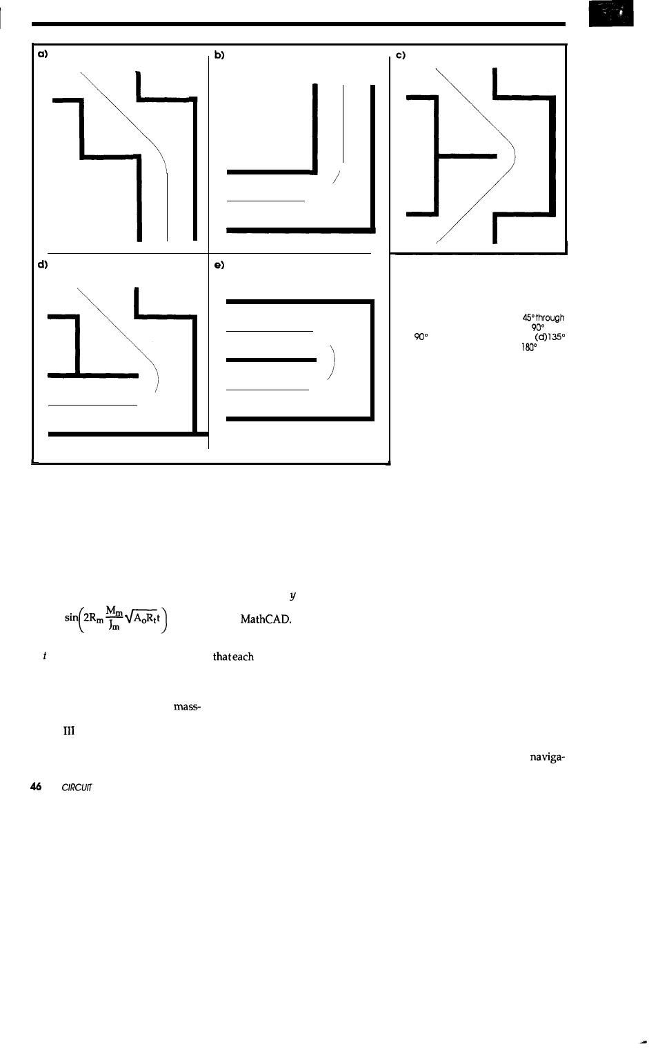
change in the differential speed, would
take an infinite force from the tires to
accelerate the inertia of the mouse in
zero time. Figure 6 shows the actual
velocity of each wheel as it goes around
a corner. It turns out that the net force
on the tires is constant if each wheel
accelerates up to the target differen-
tial velocity with a time-dependent
profile as shown:
where:
= time
Based on this equation, a mouse
should be designed with widely sepa-
rated drive wheels and a large
to-inertia ratio. Unfortunately MITEE
Mouse
has the drive wheels spaced
close together so that it can navigate
diagonals. This clearly compromises
its turning performance. The sensors,
however, are supported with a balsa
wood frame to minimize their contri-
bution to the inertia of the mouse.
During the time the mouse is ac-
celerating to full differential velocity
it is going on a circle with a constantly
diminishing radius. To determine the
distance the mouse travelsduring this
phase, the x and components of the
velocity were numerically integrated
using
This information is
then stored in a table and used by the
turn-profile generator to make sure
tumisinitiatedat thecorrect
position to complete the turn in the
center of the square and heading in
the correct direction.
There are five types of turns re-
quired by MITEE Mouse III when
making its high-speed runs through
the maze. These are shown in Figures
7a to 7e. Each of these has a different
1
Figure 7-The five basic turns through a
micromouse maze include (a)
a diagonal, (b) straightforward
turn,
(c)
turn through diagonals,
through a diagonal, and (e) a
U-turn.
radius and therefore different aver-
age and difference velocities. The
straight-profilegeneratorcheckstosee
the type of turn required at the end of
each straightaway and sets the final
velocity of the straight equal to the
average velocity for that type of turn.
The turn-profile generator then uses a
look-up table to find the other para-
meters of the turn and generate the
appropriate turn profile.
As with the straight-profile gen-
erator, the turn-profile generator has
information on the speed and accel-
eration of each wheel and therefore
generates feed-forward information
that is later used by the motor control
routines.
NAVIGATION
Perhaps the most difficult part of
building a micromouse is the
CELLAR INK
tion. It is often left until last and can-
not be tested until the other systems
are operational, but it determines to a
great extent the capability and relia-
bility of the mouse. For humans, navi-
gation comes naturally. By collecting
information with our eyes and recog-
nizing what we see, we can walk, run,
or drive a car in a straight line or
around a corner without much diffi-
culty. A micromouse, by contrast, does
not do so well. For its size it goes quite
fast. MITEE Mouse III may hit 8 MPH
on a
straight. If we scale its
speed according to its size, this is
equivalent to driving a car down a
road at almost 200 MPH, looking out
the side window and trying to keep
the car exactly 3 feet from the curb.
The first
of navigation most
mice employ is to measure position
from their wheels. By knowing the
wheel diameter and measuring the
number of wheel rotations, a good
estimateofpositioncanbemaintained.
This works very well at low speed
when the tiresarenot slipping. MITEE
Mouse III can go 10-15 squares with-
out any other correction if it is prop-
erly aligned at the start. What it can-
not do, however, is search the whole
maze and then do a speed run without
additional corrections.
The eyes of the navigation system
are the sensors. On MITEE Mouse III,
they are made up of twelve focused
infraredemitterdetectorpairslocated
in linear arrays at the four comers of
the mouse. If a wall or post is located
directlyunderanemitter-detectorpair,
light from the emitter will reflect back
from the surface and turn on the de-
tector. If only the floor
is
directly
under
an emitter-detector pair, the detector
will remain off. Both the tops of the
walls and the tops of the posts look the
same to the sensors. Figure 8 shows
the detectors that are turned on by
different wall conditions.
Once the detector signals are re-
ceived by the processor, they are con-
verted into a distance or clearance.
This clearance is measured in units of
emitter-detector pair spacings (0.2
inches) and represents the position of
the detector, closest to the mouse, that
is turned on. A clearance of 12 means
that all the detectors are off and there
is no wall under any part of the array.
A clearance of 0 means that at least the
detector nearest to the mouse is on.
There are three basic types of er-
rors the mouse must recognize and
correct. These are called forward er-
ror, heading error, and offset error.
The first of these, forward error, is
illustrated in Figure 9a. It is usually
detected by openings in the walls on
either
themouse. When
no wall or post under a sensor array,
none of the detectors are turned on.
When any of the detectors first turns
on, it defines the leading edge of a
wall. The trailingedgeisdefined when
the mouse passes over a wall and the
last detector is turned off. The posi-
tion of the wheels is recorded at each
leading and trailing edge.
Figure 8-Mouse-to-wall
distance can be
determined
by how many sensors are ac-
tive. Intersections can a/so be detected.
The rules of the contest specify
that there must be a post at the four
corners of every square. The sensors
for MITEE Mouse III aredesigned such
that the four posts will be directly
under the four sensor arrays when the
mouse is in the center of a square. As
the mouse enters a square, the sensors
should detect a leading edge when the
mouse is half a post width from the
center and detect a trailing edge when
the mouse is half a post width past the
center. Any difference between the
expected and measured leading and
trailing edges is an error. The
8031 In-Circuit
Emulation
Our emulator provides most features
of an 8031 In-Circuit-Emulator at a
significantly lower price. It assists in
integration, debug, and test phases of
development. Commands include:
disassembly, trace, breakpoint,
alter register/memory, and load Intel
Hex file.
8051 Simulation
The 8051 SIM software package
speeds the development of 8051
family programs by allowing
execution and debug without a
target system. The 8051
is a screen oriented, menu
command driven program doubling
as a great learning tool.
Single
Board Computer
A
fast and inexpensive way to
implement an embedded controller.
8031132 processor,
parallel
up to 2
serial ports,
volt
operation. The development board
option allows simple debugging of
family programs.
Prototyping
System
The IPC-52 development system
allows you, the designer, to
concentrate on Application Specific
Circuitry only, because the 8052,
EPROM, and
sections are
and fully functional. The
prototyping bread-board is
integrated into the system save
days of development time. $220
Call us for your custom
product needs.
Other products available:
GAL Programmer $199
FORTH Card FORTH development
card for STD Bus $279 (OEM-$1 99)
(619)
August/September 1990 47
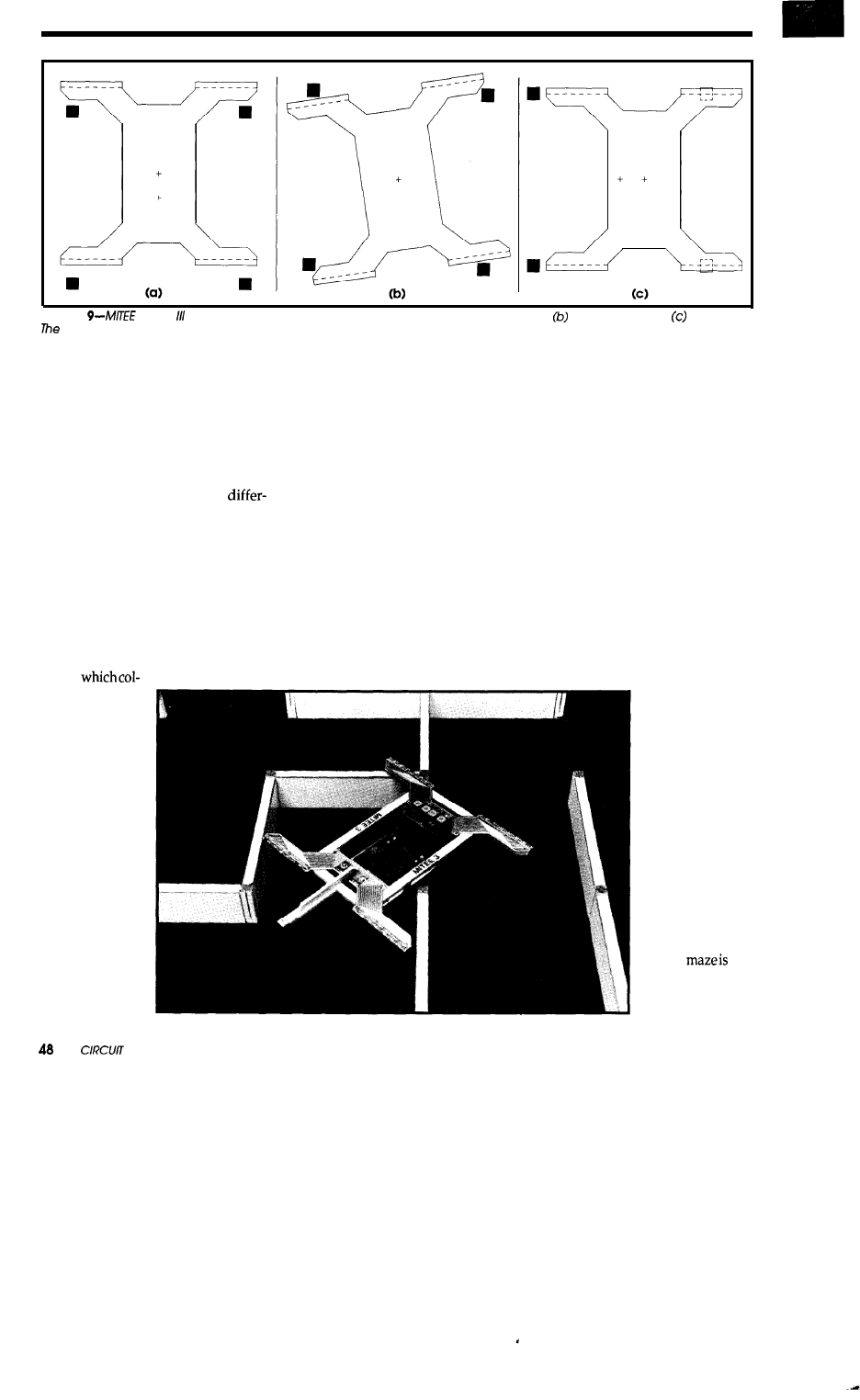
Figure
Mouse recognizes three types of positional errors including (a) forward error,
heading error, and
offset error.
squares represent the four corners of the maze square and the crosses represent ideal position and actual position.
urements from the four sensor arrays
are averaged to correct the forward
error. To make sure that no edges are
missed, MITEE Mouse III is pro-
grammed to start looking for edges 4
cm before it reaches the center of a
square, and continue looking until 4
cm after it leaves the center.
The forward error is the
encebetween where the mouse thinks
it is and where it actually is. This can
be corrected by updating where the
mouse thinks it is. Since this does not
involve any mechanical motion, it can
be done instantaneously.
If the sensors were perfect, they
would detect a wall only when it was
located directly below them. The in-
frared emitters and detectors use
lenses
limate and focus
the light, but the
sensors still de-
tect the wall
slightly before
and after it is di-
rectly
under
them. This gives
an effective wall
width, as seen by
the
sensors,
which is slightly
greater than the
actual width.
This is not a
problembecause
it can be com-
pensated for by
software. A
problem does
arise, however, when some sensors
are more sensitive than others and
pickup the wall sooner and see it later.
Also, in spite of circuitry specifically
designed to suppress ambient light,
there are some second-order effects
which change the sensitivity of the
detectors due to ambient light. Lastly,
the sensitivity
is
affected by the height
of the sensor above the walls. Both
rocking of the mouse on its wheels
and variations in the fabrication of the
maze aggravate this problem. To keep
the software simple, a single value of
effective wall width is used, even
though this guarantees an error with
some sensors. This error is mitigated,
however, because in many cases the
sensor which first picked up a wall
will also be the last to see it. If the
positions of the leading and trailing
edge are averaged, the width of the
wall drops out and the true center is
correctly determined.
On a long straight section there
may not be any openings in the side
walls. Under these circumstances there
may be no leading or trailing edges
from which to correct the forward er-
ror until the very last square where
the mouse must turn left or right. The
mouse must rely on its tire measure-
ments. Unfortunately, long straight
sections are where the mouse reaches
the highest velocity and the tire meas-
urements are the least accurate. In ad-
dition, the maze is often made of sec-
tions or quadrants and these quad-
rants join in the
middle of the
longest straights.
Itisoftendifficult
to adjust the
quadrants so that
the joints are flat.
As a result, the
mouse bounces
up when it hits
the joint, loses
track of exactly
where it is, and
cannot correct the
error until it is
almost too late. A
carefully ad-
justed
the
best solution to
this problem, but
if the maze is
CELLAR INK
warped, it may not be possible to ad-
just it for low error over the full length
of each piece. To compensate for this,
MITEE Mouse III is programmed to
perform its first speed run with a low
maximum velocity in case there are
any bad bumps. The maximum veloc-
ity is then raised for all subsequent
runs, so that if the maze is flat, the
mouse will realize its best possible
time.
The second type of error, heading
error, is illustrated in Figure 9b. It
represents a mistake in the direction
the mouse is traveling. It is very seri-
ous because the mouse will crash if it
is not corrected. The heading error is
easy to correct, however. If the mouse
wheel chair design, such
as MITEE Mouse III, one wheel must
simply turn faster for a period of time
and the other turn proportionally
slower. If the mouse is standing still,
the heading can still be corrected. One
wheel must turn forward a fraction of
a turn and the other turn backward by
the same amount. The mouse will
rotate in place and the heading will be
corrected.
The third type of error, offset er-
ror, is illustrated in Figure When a
mouse is traveling down a straight
section, but is not in the center of the
track, it has an offset error. Offset er-
ror is less serious than heading error
because an offset error alone will not
cause the mouse to crash. It is more
difficult to correct, however, because
the mouse is not able to translate di-
rectly to the side. To correct an offset
error the mouse must first generate a
heading error, travel with that head-
ing error until the offset error is cor-
rected, and then correct the heading
error.
Heading and offset errors are of-
ten dealt with together because the
same set of measurements are used to
calculate both. During the time the
mouse is looking for leading and trail-
ing edges, it also keeps track of the
minimum clearance on each of the
four sensor arrays. These measure-
ments are used to calculate the head-
ing and offset errors.
heading error
LFC RFC LBC + RBC
2
offset error =
LFC RFC + LBC RBC
2
where:
= left front clearance
= right front clearance
LBC =
left back clearance
RBC =
right back clearance
In contrast to forward errors,both
of these errors cannot be corrected
stantaneously.Theinertiaofthemouse
limits how quickly the heading
corrected. MITEE Mouse III tries to
correct the headingbefore it travels an
appreciable part of one square. It uses
an acceleration for the
tion which is proportional to the ve-
locity it is traveling. When it is going
slowly, it corrects slowly; when it is
moving fast, it corrects quickly. The
offset error has all the limitations of
the heading error and, in addition,
distance is required for the offset to be
corrected. MITEE Mouse III is pro-
grammed to correct the offset error in
exactly one square. It generates a
heading error that will exactly cancel
the offset error by the time the next
clearance measurements are made.
Because the clearance measurements
are made from the posts and not the
walls, new heading and offset errors
GET TO WORK!
A New Project
Our line of macro Cross-assemblers are easy to use and full featured,
including conditional assembly and unlimited include files.
Get It To Market--FAST
Don’t wait
until the hardware is finished to debug your software. Our
Simulators can test your program logic before the hardware is built.
No Source!
A minor glitch has shown up in the firmware, and you can’t find the
original source program. Our line of disassemblers can help you
re-create the original assembly language source.
Set To Go
Buy our developer package and the next time your boss says “get to
work”, you’ll be ready for anything.
Quality Solutions
PseudoCorp has been providing quality solutions for microprocessor
oroblems since 1985.
BROAD RANGE OF SUPPORT
.
Currently we
support
the following microprocessor families (with more in
development):
Intel 8048
RCA
Intel 8051
Intel
Motorola 6800
Motorola 6801
Motorola
Motorola 6805
Hitachi 6301
Motorola
MOS Tech 6502
WDC
Rockwell
Intel
Zilog
NSC 800
Hitachi
Motorola
Motorola 68010
All products require an IBM PC or compatible.
Cross-Assemblers
as low as
Simulators
as low as $100.00
Cross-Disassemblers
as
as
Developer Packages
as
as
(a $50.00 Savings)
So What
Waiting For?
Professional Development Products Group
716 Thimble Shoals
Suite E
Newport News,
VA 23606
(804) 873-1947
August/September
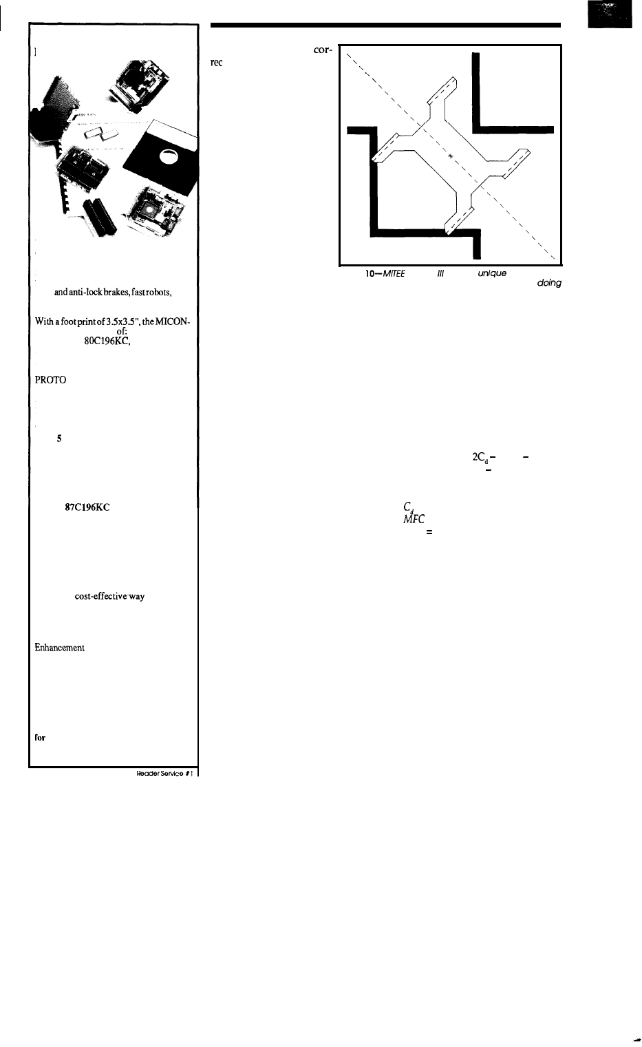
MICON-196KC
DIGITAL CONTROLLER KIT
The MICON-196KC Digital Controller
can be used in applications such as: high
speed closed loop motion control, mid-
range digital signal processing, high speed
positioning control, traction control sys-
tems
high
speed data acquisition, etc.
196KC Kit consists
a CPU Module
featuring the
Intel’s 16 bit/l6
MHz embedded controller; a MEMORY
Module containing 64K EPROM/RAM
with customized memory mapping; a
Module supplied for customer’s
application specific circuitry; two BUS
Modules, a Firmware/Software support
package, and a User’s Manual.
The MICON Kit can be configured in at
least different modes: as a low-cost
software development tool in conjunc-
tion with any IBM PC-AT or compat-
ible; as a learning tool using applica-
tion-oriented tutorial software; as a
hardware prototyping environment
for
customized
I/O; as an EPROM burner
for the
microprocessor; or
as a READY-TO-USE digital control
solution for your applications.
The MICON-196KC is aimed to restruc-
ture the relationship between HARD-
WARE/SOFTWARE/APPLICATION
engineers, and to build Inter-Disciplinary
bridges. This product is OEM-Ready and
provides a
to start BIG
PROJECTS with SMALL BUDGETS!!!
MICON-l%KC sells for $299.00
(Additional Hardware and/or Software
Kits
for MICON-196KC are
also available.)
MICON
5270 Elvira Road, Bldg. 104
Woodland Hills, CA 91364
Phone (818) 348-4992
Fax (818) 348-0960
Intel is a Registered Trade Mark
Intel Corp.
IBM PC-AT is
a
Registered Trade Mark
for
IBM Corp.
51
can be
calculated and
ted every square regard-
less of the maze design.
Though heading and
offset errors are calculated
from the same measure-
ments, it is important to
separate these two types of
errors, particularly
before
a
90” turn. This is due to the
fact that a headingerror will
still be a
heading
error
after
a turn, but an offset error
will become a forward er-
ror. Also any forward error
will become an offset error.
Forward errors are gener-
ally well corrected before
entering a turn, so there
should be no offset error
after the turn. Offset errors
by
contrast,
cannot becorrected if they
are detected just before a turn. They
should not be a problem, however, be-
cause they will become forward er-
rors after the turn and forward errors
are easy to correct. With this in mind,
MITEE Mouse III is programmed to
ignore offset errors if the next move is
a turn.
Figure
Mouse
has the
ability to run
diagonally, so must be able to collect data while
so.
DIAGONAL NAVIGATION
moves forward the right rear sensor
array will start to pick up a second
corner. The minimum clearance and
wheel position at minimum clearance
is also recorded and stored. The two
wheelpositionmeasurementsareused
just like the leading and trailing edge
measurements to correct the forward
position. The
minimum
front and rear
clearances are used to calculate the
heading and offset errors.
MITEE Mouse III requires an
additional type of navigation not re-
quired on most mice: the ability to
navigate diagonals. Since the mouse
is not running parallel to any walls,
this may appear difficult at first, but it
turns out to be quite simple. The pro-
gram for diagonal navigation is less
than half the length of the program for
normal navigation.
heading error =
MFC MBC
offset error = MBC MFC
where:
= clearance on a diagonal
=
minimum front clearance
MBC
minimum back clearance
The same type of error detection
and correction-forward, heading,
and offset-are required for diago-
nals as for straights. The difference is
in how the required data is collected.
Figure 10 shows MITEE Mouse III
running down a diagonal. The left
front sensor array is starting to pick
up a corner. As the mouse moves for-
ward, the clearance will get smaller
and then larger. As with the straight
navigation, the minimum clearance is
recorded and stored. The wheel posi-
tion when the clearance was at a
minimum is also saved. As the mouse
If the left front and right rear
sensors are used to make the clearance
measurements for one square, the
adjacent square will use
the right
front
and left rear sensors. The corrections
work very well but are less precise
than those for straight navigation for
several reasons. First, they are based
on two measurements instead of four,
resulting in more noise in the meas-
urements. Secondly, the total clear-
ance on each side of the mouse is only
0.6 inches. The resolution of the sen-
sors is one emitter-detector pair or 0.2
inches. A resolutionof one third of the
clearance does not allow precise cor-
rection.
50
CIRCUIT CELLAR INK
The third reason is more subtle,
and is due to the placement of the
sensors. They are not optimized for
diagonal operation and cannot simul-
taneously measure the position of a
corner in front of the mouse and be-
hind it. The front comer is measured
first and a short distance later the back
corner is measured. We assume that
the mouse travels in a straight line be-
tween the two measurements. The re-
sulting heading and offset measure-
ment was valid when the mouse was
centered between the two comers but
may not be valid now that the mouse
has traveled farther. In fact, if the
mouse had a heading error when it
was centered between the comers, it
has been traveling on an incorrect
heading since then, and has an offset
error by the time the measurement is
finished. If we know the distance that
the mouse has traveled since it was
centered, we can estimate the result-
ing offset error and add that to the
offset error measured when the mouse
was centered. The heading error re-
mains the same as the value when it
was centered. If the corrections are
then performed on the combined off-
set error and original heading error,
the stability of the corrections, par-
ticularly for large errors, is signifi-
cantly improved.
Nevertheless the maximum ve-
locity of the mouse is usually limited
on diagonals to give the mouse time to
correct each error as it is detected. The
time saved by going directly down a
diagonal more than offsets the loss of
time due to limiting the maximum
velocity.
. ..AND ONWARD
Armed with the information in
this article and the related computer
programs available through the Cir-
cuit Cellar BBS-information which I
have spent the last five years putting
together-a newcomer to the
mouse arena will hopefully become
competitive in a much shorter time.
Accordingly, I hope to see the day
when MITEE Mouse III clones are
beatingtheoriginalandmakingagood
account of themselves on the world
scene. To those of you who are not
interested in micromice but insist on
applying all this high-performance
stuff to some ungainly robot, slowly
ambling toward the outlet in their
living room-it’s not what I had in
mind, but if it is helpful, great!+
I would
like to acknowledge the help
of Tony
Caloggero
who built all the mechanical
for
Mouse
Andy Goldberg
who worked on the maze solver, even when his
doctoral thesis was on the line, and Leo Casey
who was my constant sounding board and
helped with the navigation. Without their help,
there would have been no mouseabout which to
write an article.
David ten is a principle
engineer
in
the Laboratory for Electromagnetic and Elec-
tronic Systems at the Massachusetts Institute
of
Technology. He holds a B.S. and M.S.
degree from
IRS
2 10 Very Useful
2 11 Moderately Useful
2 12 Not Useful
MS-DOS EPROM
PROGRAMMING
NEEDS NO
CONNECTS TO YOUR SYSTEMS
PARALLEL PRINTER
A FULL FEATURED, EASY-TO-“SE SYSTEM WORKS ANY
STEM
CARD
28256’
8742’
M’c
‘Socket Adapter
Required
SYSTEM SOFTWARE
PROGRAM EPROM(S)
l
SAVE EPROM S OR
FROM DISK FILE
BUFFER TO
l
VERIFY
FILE INTO . PROGRAM EPROM(S)
ERASED
FROM BUFFER
. BUFFER EDITOR
INTO . COMPARE EPROM(S)
l
SELECT
TYPE
WITH BUFFER
. DEVICE CHECKSUM
HAS 18 BYTE LEVELCOMMANDS FOR DETAILED OPERATIONS
SYSTEM INCLUDES: PROGRAMMING UNIT, POWER PACK,
CONNECTING CABLE. OPERATION MANUAL SOFTWARE
$239
SOFTWARE AVAILABLE ON 3
DISK
TO ORDER SEND CHECK, MONEY ORDER,
OR CALL.
ANDRATECH
VISA
P.O. BOX 222
MILFORD, OHIO 45150
(513) 831-9708
CALL OR WRITE FOR MORE
ADD
14.00 COD
The ideal solution for embedded control
applications and stand-alone development.
l
BASIC CPU
l
Serial printer output and 5, 8 bit
ports
l
5
prototyping
l
Memory: 8K RAM, expandable to
l
Power requirements:
300 ma. only
l
PROM
socket for 2764 or 27128 EPROM
l
handling capability
l
Built to exacting standards and warranteed
l
$228.00 including documentation (quantity
Call
now!
603-469-3232
Binary Technology, Inc.
Street . PO Box 67
NH 03770
August/September 1990
Huge Arrays on the
Taking Advantage of Memory Management
t
H
itachi’s HD64180 (and its
little microcontroller brother, the
are sometimes used in
applications where huge quantities of
data are collected or analyzed. Their
them
perfect for battery-powered data ac-
quisition equipment. Or, as part of an
instrument, their architecture is ideal
for storing large amounts of data
during analysis.
As I mentioned in a previous ar-
ticle, these processors include a pow-
erful Memory Management Unit
designed to extend the ad-
dress space to a full megabyte. With
some understanding of the intricacies
of the MMU, it’s not too hard to up-
grade an old
application to make
use of the
extra memory.
Of course,
the HD64180 still uses a 64K logical
address (for compatibility with the
so a
program doesn’t sud-
denly get a nice
linear address-
ing range. The software must be
somewhat restructured if huge pro-
grams or data areas are needed.
(As a refresher, “logical” ad-
dresses are those issued by the pro-
gram; on the HD64180 these can never
exceed
the limit imposed by us-
ing
addresses in load and jump
instructions. “Physical” addresses are
those appearing on the CPU’s pins;
the internal Memory Management
Unit converts Logical to Physical,
using a translation algorithm con-
trolled by the programmer.)
Suppose you’re designing a
remotedata collection device that gets
one
ADC reading
every
second.
This doesn’t sound like much data,
but after only a day the system will
have acquired 86,400 words (172,800
bytes&-far more than the logical
address space of 64K.
in this sort of application demands
careful
analysis
of both the logical and
physical addressspaceneeds. There is
no way all 176K will fit within the 64K
logical space, so the program will have
to remap the MMU, possibly often, to
get to the array.
ACCESSING ARRAYS
This
problem
requires
“sequential” access to the data, since
the current data point is appended
immediately
after
It special
case of the more general array
accessing situation, where a program
might need any arbitrary data point,
in no particular order.
Byte-oriented data (like strings) is
easy to work with. Element I is the
“Ith” address in the string; that is, the
address of
is the start address
is a valid element). This is called a
vector-it has only one dimension:
that given by the subscript.
Of course, in real applications we
often workwithdata
bits long. Integers are often two bytes;
floating-point values typically are four
or even eight bytes. Array element of
a vector is found from:
base + I x (element size)
where
is the start address of the
array.
Again, this assumes element 0 is
valid. Element 0 is at the first address
of the array, followed sequentially by
each other element.
Multidimensional arrays use an
extension of this formula. In most
systems thesearrays are stored in “row
major” order: given
all column elements of row Oare stored
first, then the column elements of row
1, and so on. We can get to any element
using the formula:
address = base + I x (Jmax x Esize)
+
is the number of columns in the
array and
Esize
is the number of bytes
per element of the array.
As you can imagine, this can be a
computationally expensive way to get
to an array. Multiplications are slow.
The
multiply instruction
only handles
operations, and so
by itself it is not adequate for indexing
into an array. Generally you can count
on the quantity
x
Esize) to
be a
constant;
for
speed-critical
applications, it may be wise to set this
to a convenient value (a power of two),
even if some memory is wasted.
Similarly, aim for an element size that
for multiplies.
Any number of dimensions can
be accommodated by extending the
formula. Higher dimension arrays
require even more math to access, so
try to limit the dimensions to one or
two.
In real-timeapplicationsit’s often
nice to support two forms of data
access. A perfectly general form is
useful for off-linedata reduction;your
application program can request any
array element
in any sequence. During
data acquisition you might need a
shortcut to avoid the computational
August/September 1990
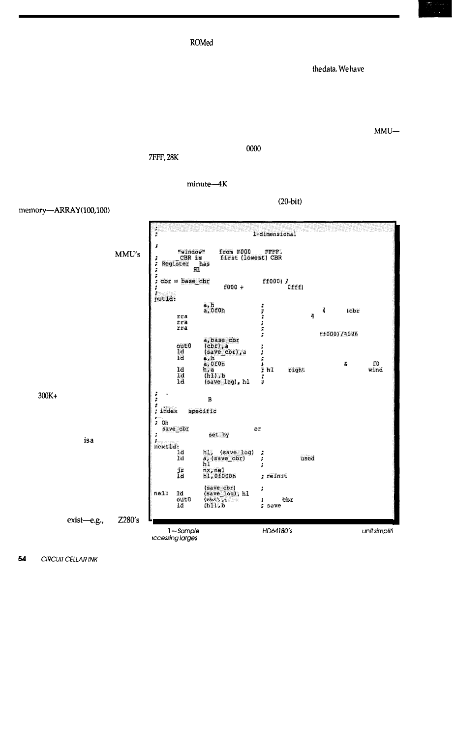
overheadofcomputinganarrayindex.
If data is gathered in some sequential
form, it‘s easy to visualize the data as
a one-dimensional vector (instead of a
multidimensional array), and store
each value sequentially. We’ll explore
both methods.
THE MEMORY MANAGER
Sure, it’s easy to write code to
compute an array index along the lines
presented. We’ll run into trouble when
the array gets too big. Suppose your
code uses most of a 27236 EPROM,
leaving only 32K of logical address
space for data. If all of this were
dedicated to a two-dimensional array
consisting of 4-byte-long elements,
then only 8192 elements fit in
exceeds
address 64K.
Here the MMU comes to the
rescue, but not without a lot of help
from the programmer. Obviously, we
can simply reprogram the
control registers every so often and
bank switch portions of RAM into the
processor’s address space. The secret
to success is careful planning.
If you’ve never really blown a
software project by immediately
jumping into coding, then you are
probably sick of hearing about
software methodologies. In fact, as
processors and programs get more
complicated, careful design
is
far more
important than it once was. Oh for the
days of 4K programs! We could crank
out a few thousand lines of code in a
couple of weeks and be done. Now,
when
programs are the norm, a
carelessly designed system will be a
disaster. Guaranteed.
This is certainly true when using
any sort of memory manager. One
penalty
of the MMU segmentation
ofyourlogical addressspace that must
be designed in up front, and that very
likely can never be changed without
completely rethinking the entire
structure of the program.
Using huge arrays forces you into
a three-bank memory model on the
HD64180 (note that on other chips
other options
the
fantastically complex and powerful
MMU will let you have up to 16 banks
in the logical address space). One bank
points to the
program; in most
cases this logical-to-physical mapping
will never change. Another bank
accesses an area of RAM for program
variables and transients. In all but
extreme cases this will never be
remapped, because the stack will
reside here. Finally, one bank points
to the huge array(s).
Figure 1 shows one possible
configuration of the memory
management unit. This assumes 32K
of ROM from logical address
to
of RAM from 8000 to EFFF,
and 4K of huge array RAM at the end
of memory.
Wait a
of RAM for
huge arrays? That doesn’t seem like
much! This 4K section of the system’s
address space is essentially a
“window“ into the huge array. The
window is for storage of huge arrays.
Never, never store the stack or other
variables here, since remapping will
invalidate
to provide
a section of logical space to allow access
to the data; the 4K window is this
section. This is much like a disk buffer
used in operating systems-data is
written to the buffer and then flushed
to disk when full. Its size is a result of
themappingresolution of the
4K is the minimum amount we can
allocate. You can always make this
larger, which will cut down on MMU
remapping, but you’ll sacrifice either
variable or program area.
The idea behind using this
window is to compute the physical
address of the proper array
element, and then to position the
Put an element in a huge
array.
; Here we assume:
: The
is
to
BASE
the
value
B
the data to store
Register
has the array index
t (index AND
4096
logical address=
(index AND
Id
get high order index value
and
mask off upper bits
bits)
shift right bits
{since we ignore lower 8 bits,
this is a 12-bit shift)
rra
a- (index AND
add
set new cbr value
save cbr for nextld
high part of index
or
mask off high nibble or in
is
logical addr in
save data
save logical addr for nextld
ret
put register In the huge dimensional array at the next
open location. This assumes that putld was once called to
a
value.
.
entry, B is the data to store
;
was set by putld
nextld
save-log was
putld or nextld
last logical address used
inc
last cbr
skip to next element
; jp if not exceeded the window
to start of the window
inc a
; next cbr value
Id
save current
cbr
,a
; save current logical address
set
data
ret
Ming
code shows how the
memory management
blocks of data.
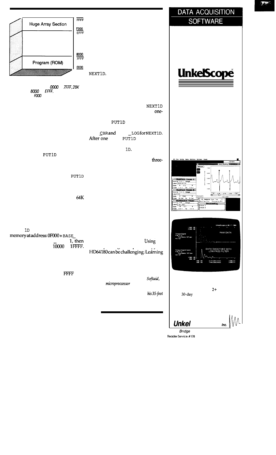
Program Data and Stack
Figure 1 -One
possible MMU configuration
has 32K of ROM from
to
of
RAM from
to
and a 4K array
window from
to FFFF.
window to bring the data into view.
Earlier we saw how to compute an
index into any array. Now, this
windowing step is also introduced.
The algorithm is not complex, but a
wise programmer will insulate his
code from the machinations of array
element lookup by hiding the details
in subroutines.
The routine
stores a byte
to a huge one-dimensional array using
the map shown in Figure 1. The code
to get a byte from the array is nearly
identical and so is not shown.
accepts an array index in HL that can
range all the way up to 64K. Thus, the
one 4K window in logical address
space gives the routine access to a
hunk of data. Note that it supports
random accesses-it stores the data in
B into the array at the index in HL. HL
can be 12 on one invocation and 40000
on the next.
PUT
locates thearrayinphysical
C B R
*
4096. Thus, if
BASE CBR
is
the array runs from
to
This implies that the memory
manager’s CBAR register must be set
to Fx (where “x” defines the logical
start of the base area) so that logical
addresses from FOOO to
(our
window) are translated into common
area 1.
For the sake of simplicity, the code
stores a one-byte value. A word
version would require the “index” to
be multiplied by two before it is used
in the computations. Use a shift to do
themultiply,butbewaryofoverflows.
Multiple-dimension arrays can be
programmed just as easily, but you
must compute theactual array address
using the formula previously
discussed.
Multipliesare slow and should be
avoided; try to pick values of Jmax
that are powers of two, and then use a
series of shifts. Fast access will require
some thought to optimize the
computations.
One easy speed trick is shown in
Especially when gathering
data, we often just put one value in the
next location-random array accesses
are not needed. This means we can
skip all of the multiplications needed
to compute the address; we just
increment the last address.
illustrates this approach with the
dimensional array we’ve already
looked at.
saves the current
CBR and logical addresses in
SAVE
SAVE
call to
to set things
up, all further sequential accesses can
use the faster
NEXT
With the single
indexes
shown,
the speed difference
is not important; with a two- or
dimensional array, a tremendous time
saving will result.
What if your program uses a
number of
big
arrays?
You can’t assign
more windows since the HD64180
limits mapping to three sections.
Probably
the
easiest
solution is to write
a PUT and
GET
routine for each array,
using a different
BASE
CBR
value for
each. Avoid using sequential accesses
unless you can be really sure that the
accesses will be restricted to one array
at a time.
Large arrays are a necessary part
of many software solutions.
the
memory
management
provided by the
to use the MMU effectively gives you
a powerful tool on a powerful
processor.+
Jack Ganssle is the president of
a
vendor of
development tools.
When not busy pushing electrons around, he
sails upanddown the East Coast on
sloop.
IRS
2 13 Very Useful
2 14 Moderately Useful
2 15 Not Useful
We’ll never
leave you
without
a trace
UnkelScope is an easy-to-use,
menu-driven software package
that will always leave you with
a clear, accurate trace. Whether
you’re in a laboratory or on
an oil rig in the North Atlantic,
UnkelScope will get the job done
l
Full hardware speed
l
Real-time X-Y plots
l
Graphical Editing
l
Data Processing
l
Experiment Control
l
Plus much more
MAC
Version
PC Version
UnkelScope JUNIOR
$125
UnkelScope for MAC
$149
UnkelScope Level
$549
money-back guarantee
(617) 861-0181
FAX (617) 861-1850
Software
62
Street Lexington, MA 02173
August/September 1990 55
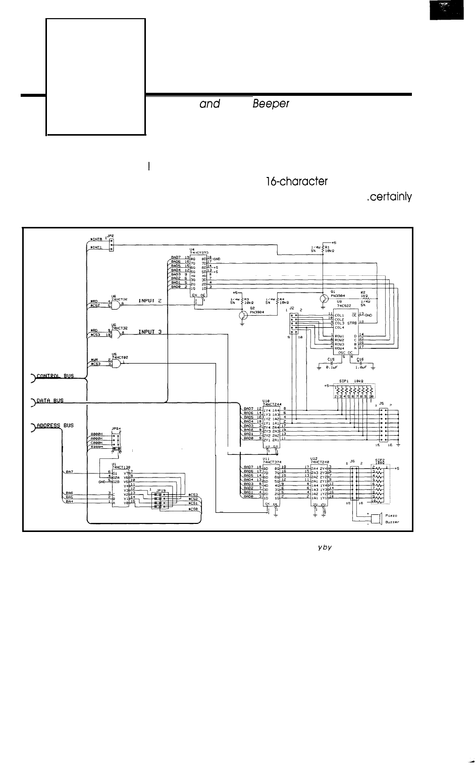
FIRMWARE
FURNACE
The Furnace Firmware
Ed Nisley
Project
Keypad
Piezo
0
nce upon a time, built an 8031 gadget with no inputs. It would pick a
witticism from EPROM and scroll the text across a
LCD panel, then
go to sleep for awhile. You couldn’t do anything except turn it off..
the most (deliberately!) annoying gadget I’ve ever put together.
OUTPUT 3
ADDRESS DECODER
III
Figure 1 -Jhe two shift keys modify the byte returned by the other 14 keys. Either or both shifts con be pressed along with any other
key. Data values are shown in hex and ASCII (where prin table). You can assign any byte value to any ke changing the appropriate
lookup table entry.
56
CIRCUIT CELLAR INK
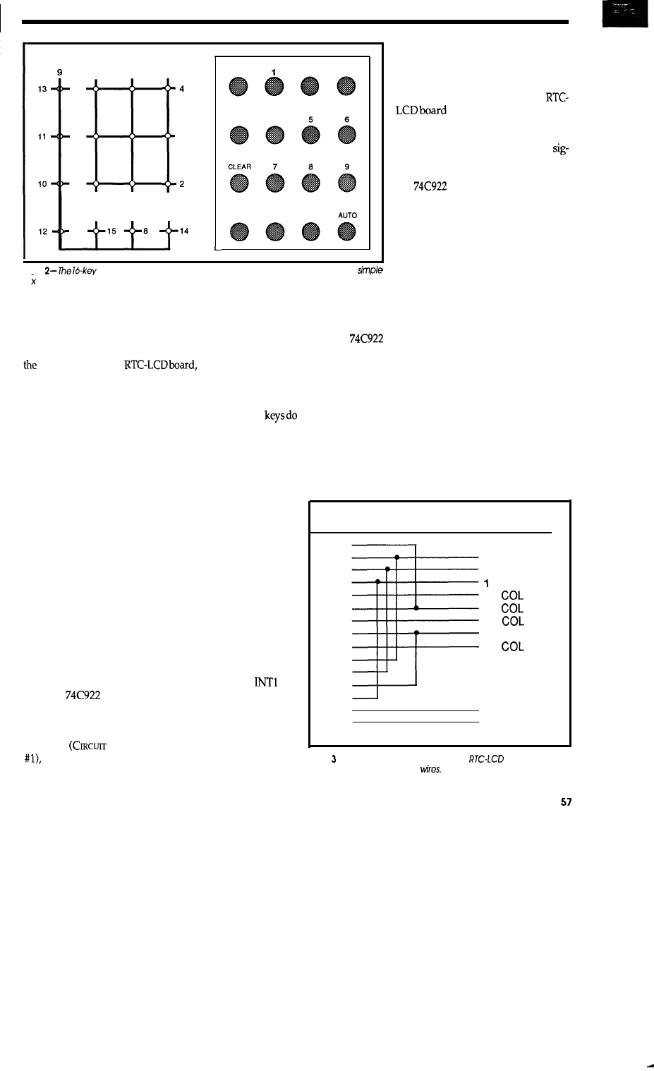
5
6
7
1
n
3
MEMORY
ACCESS
2
3
ENTER
4
SCAN
M O N I T O R 0
for other, higher-priority functions,
so I am using simple polled input.
Although the STROBE signal can be
read through one of the INT bits, I
added an extra wire to the stock
torouteitintodatabit 6,as
shown in Figure 1.
It seems as though this can’t pos-
sibly work, because the STROBE
nalclocks thedatainto the’373 latches.
However, the two transistorsbetween
the
and the ‘373 add enough
delay to ensure that the STROBE sig-
nal is latched at a logic zero when you
release the key. The ‘373 latches track
their inputs when the clock input is
high, so you can read both high and
low STROBE inputs right through the
Figure
keypad is laid out in a 4 x 4 matrix, but with wiring that isn’t a
latch!
4 4
array.
My ongoing Furnace Firmware
project, on the other hand, requires
some way to set parameters, select
displays, override defaults, and so
forth. The LCD interface I described in
last issue uses the
so it’s only natural to put the keypad
hardware on that board to good use.
However, in order to demonstrate
some hardware and firmware tricks, I
will use a keypad that requires some
tinkering.
No control system is complete
without an audible alarm of some sort,
so this part of the project includes a
piezoelectric beeper. It sounds off
when you press a key, so you know
when the system has accepted (or re-
jected!) your input.
HARDWARE ENCODING
The hardware starting point is the
RTC-LCD keyboard interface shown
in Figure 1. Under ordinary circum-
stances, you plug a matrix keypad
into J2 and you’re up and running. Be-
cause my keypad isn’t quite standard,
we need to understand the circuitry
on the board so we know what to
modify.
The
keyboard encoder
scans up to 16 keys arranged in a 4 x 4
matrix. In much the same way as I de-
scribed in the very first Firmware
Furnace
C
ELLAR
INK,
issue
the chip lowers one column out-
put and examines the four row inputs
to see if any are low. If none are, it
proceeds to the next column.
MAKING CONNECTIONS
When you press a key, one of the
row inputs goes low and the
stops scanning at that column. It puts
the binary code corresponding to the
key’s location on the data outputs and
sets the STROBE output high. Scan-
ning resumes when you release the
key, so two
not conflict. If you
press two keys in the same column at
the same time, the chip returns the
code for one key or the other, but not
both, and waits for you to release it
before processing the other.
Figure 2 shows the layout of my
keypad. There are 16 keys laid out in a
4 x 4 matrix, but the wiring is not a
simple 4 x 4 array. The labels printed
on the keypad reflect the design of a
long-gone commercial product and
don’t match the functions I’ll need.
The keypad has an adhesive backing,
so mounting it to a panel is a simple
matter of cutting a slot for the ribbon
cable.
The numeric keys are a true 3 x 3
matrix and the “0” key can be wired
Jeff designed
the
RTC-LCD
board to work
with programs in
either assembly
language or BA-
SIC-52, and with
either polled or
interrupt input.
The STROBE sig-
nal latches the
chip’s output in
the ‘373 register
and can cause an
interrupt on either
INTO or
de-
pending on how
jumper JP2 is con-
figured.
The Furnace
Firmware hard-
ware needs both
interrupt inputs
KEYPAD
1
2
3
4
5
6
7
8
9
10
11
12
13
14
15
RTC-LCD J2
5 ROW 3
3 ROW 2
ROW 1
2
1
4
2
6
3
7 ROW 4
8
4
9 SHIFT A
10 SHIFT B
Figure
-Attaching the keypad to the
board requires
some cross-connection of
August/September 1990
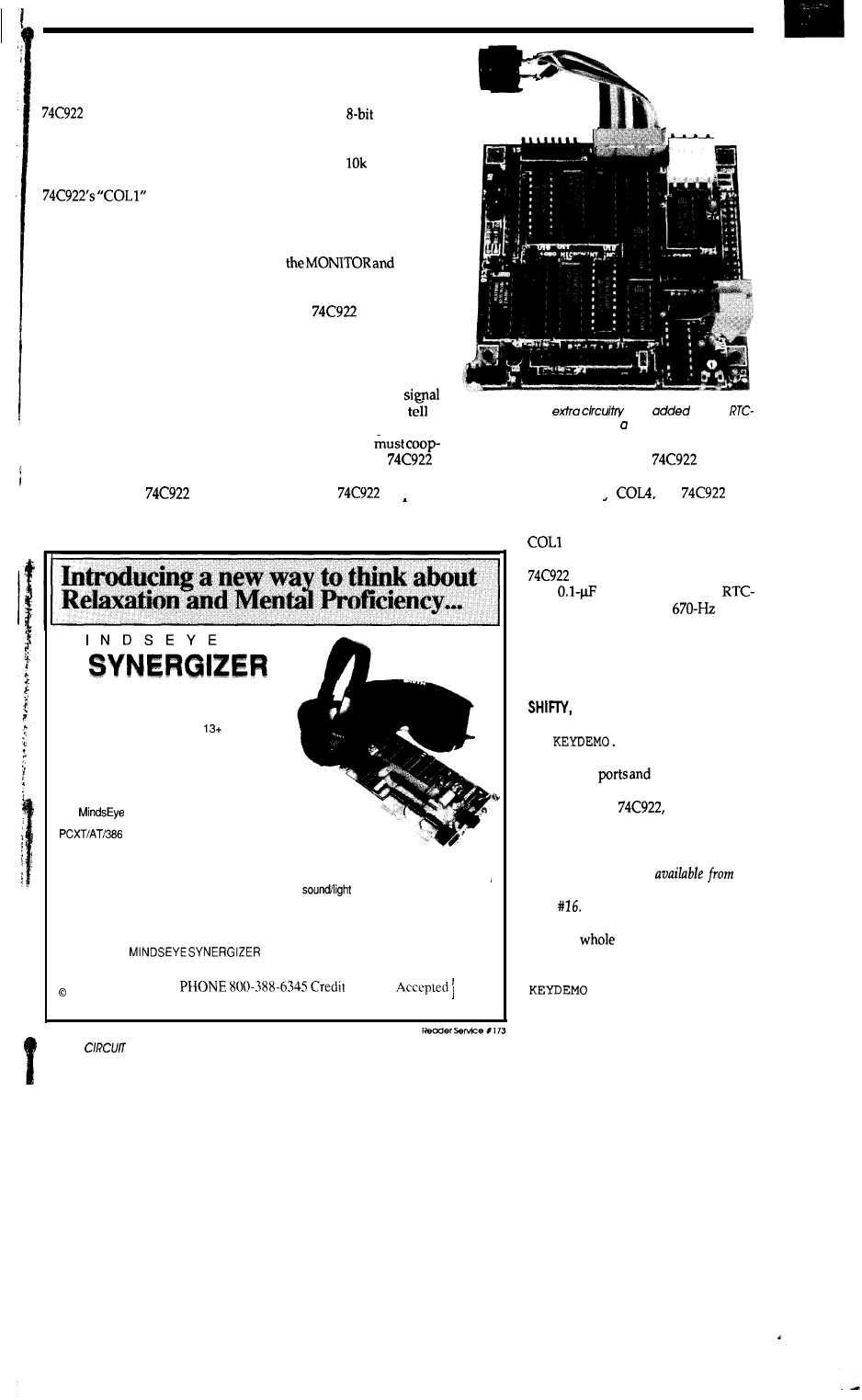
up as the last row of the middle col-
umn. The left-hand function keys
become the fourth column, but the
can encode only four of the six
keys connected to the common wire.
Figure 3 shows the external connec-
tions used to mate the keypad to the
RTC-LCD board. Notice that the
output connects to
the second keypad column and
“COL4” drives the first column of the
keypad.
A quick count at J2 shows ten
wires at an eight-pin (4 rows, 4 col-
umns) connector. If you look closely
at Photo 1, you’ll find two additional
pins embedded in a blob of hot-melt
glue on the edge of the RTC-LCD
board. Jeff located J2 at exactly the
right spot to allow easy expansion,
and it seemed a shame to miss this
LCD board has an X-10
interface that uses one
input bit; Jeff threw in a
complete
input port
“just in case” someone
might need it, and even
included
pull-up re-
sistors! Figure 1 shows the
three wires leading from
J2 to that port.
That port reads the
column scan bit as well as
AUTO
key “row” lines because
the8031 must know when
the
is scanning
that column. The key sig-
nals can only go low when
a key is pushed and the
column input is low.
When the column
opportunity. Remember, I picked this is high, you can’t
if
Photo 1
-A bit of
was
to the
keypad to illustrate some tricks; you
those keys are pressed, so
LCD board to accommodate nonstandard keypad.
won’t have tomakeanychanges to the the firmware
RTC-LCD board to use a standard erate with the
to read the
keypad.
keypad.
Because the
cannot read
The
stow scanning when
lease them and the
resumes
scanning. Because the function keys
are driven bv
the
will
those two added wires, the 8031 must it detects a keypress, so the numeric scan them almost immediately after
get at them another way. The RTC- pad keys can’t register until you re- you release a key driven by any of
through COL3.
1990
O R D E R
C a r d s
Svnetic Svstems, Inc
PO Box 95530 Seattle,
Wa 98145
Ph 206-632-l 722
M
Scientific studies have long associated brainwave
activity with specific states of consciousness. Our
normal, waking state is generally associated with
Beta brainwave frequencies of
hz (pulses per
second). Relaxation and meditation are in the 9-l
2
hz
Alpha range. Deep relaxation and certain kinds
of mental imagery (creative thinking and
“superlearning”) are experienced in the
4-7
hz
Theta range. Below this lies the Delta range of
l-3
hz, produced during sleep.
The
Synergizer is a powerful
hardware/software combination that turns your IBM
or clone into a laboratory grade audio/
visual synchronizer. The Synergizer allows the user
to program sessions of almost any length and
complexity with each eye and ear programmed inde-
pendently if desired; pulses can shift from one rate to another, while different sound frequencies
are channeled left and right. Multiple time ramps and
levels (over 32,000) may be
included within a single programmed session. A stereo synthesizer makes available a variety of
waveforms, filters and other sound parameters. The Synergizer provides more programmable
capabilities than any other device available, at a remarkably low price.
above; 512 K of RAM, and a hard drive are recommended.
Requires DOS 3.0 or
$330 GOGGLES (required) $65
EXT CONTROL UNIT (optional) $95
HEADPHONES $35
58
CELLAR INK
The capacitor on pin 5 of the
sets the column scanning rate.
The
value used on the
LCD board produces a
clock,
so each column scan pulse is 1.5 ms
wide and the worst-case time to ac-
quire the shift keys is about 4.5 ms
after the triggering key goes up.
NOISY KEYS
BAS
,
shown in Listing
1, is a BASIC-52 program that reads
the keypad
displays the bits.
Lines 110 through 130 wait for a new
code from the
while line 210
waits for the chip to scan the column
with the two additional keys. That’s
all there is to it!
[Editor’s Note: Soft-
ware for this article is
the
Circuit Cellar BBS and on Software On
Disk
For downloading and ordering
information, see page 85.1
The
point
behind those two
keys is that they can serve as shift
keys. A little experimentation with
shows that there are 14
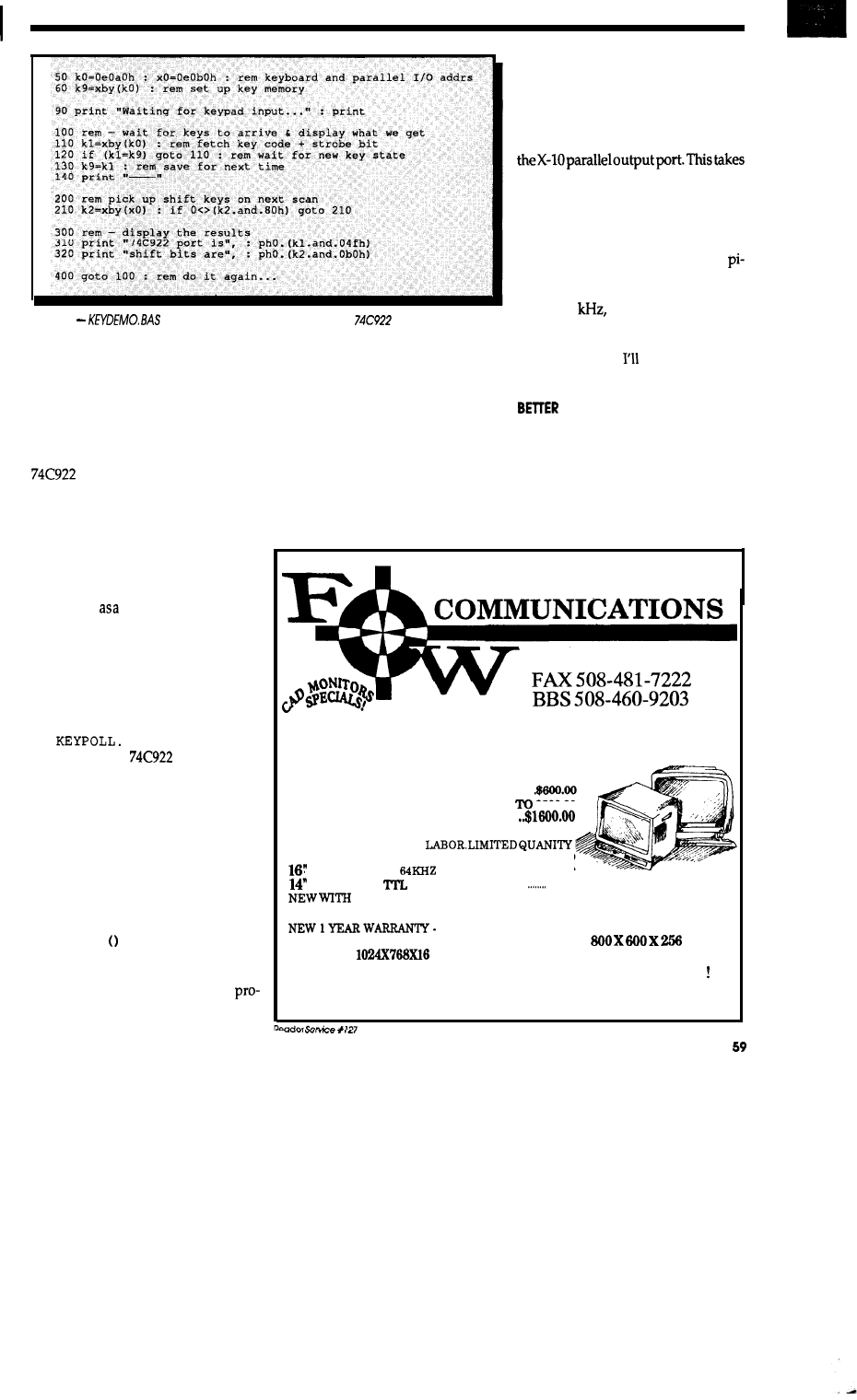
listing
1
shows how to read the keypad, The
provides
four data
bits to identify one of the 14 scanned keys; the remaining two keys are read through a
parallel input port.
scanned keys (0 through 9 and the
whole left-hand column), each of
which can have four different shift
states: unshifted, either of the two
shifts down at once, or both shifts
pressed simultaneously. Because the
doesn’t read the shift keys
directly, it will not respond when you
press them.
There are many ways to encode
shifted keys, but there is a standard
for squeezing the alphabet onto ten
keys. Photo 2 should look very, very
familiar, as the numeric pad is now
dressed up push-button telephone
keypad.Inaddition,eachof the “func-
tion keys” in the left column produce
four distinct codes. Those 14 keys,
with a little manual dexterity, return
56distinct codes! Figure4 shows what
code each key emits for each shift
state.
BAS
,
shown in Listing
2, converts raw
key code and
shift state data into a single byte. The
trick is a translation table made from a
string variable. Because the BASIC-52
manual emphasizes the “text” nature
of string variables, most people don’t
use them for anything else, but strings
can simplify many programs.
The only real difficulty is getting
nonprintable ASCII data into the
strings. The most readable solution
uses the
ASC
operator to stick a hex
value into the string, a method that
chews up a remarkable amount of
space for a each byte. In a larger
gram
the setup would take a much
smaller fraction of the total code and
be less conspicuous.
You can load the conversion table
with any values that suit your pur-
pose. I suspect I’ll change the function
key values along the way, but this
table will serve to get us going. Notice
that it does not include such niceties
as the carriage return and punctua-
tion needed to replace a standard
keyboard; adding those is left as an
exercise for the reader.
Incidentally, the “key pressed”
beep is produced by line 210, which
sends a more-or-less square wave to
advantage of another “just in case”
port Jeff included on the board. The
piezoelectric beeper is tied to all eight
data lines and their corresponding
pull-ups, as shown in Figure 2, to get
enough drive capability. Ideally,
ezo beepers should be driven by a
signal at their resonant frequency,
usually 2
but line 210 produces
about 160 Hz. As a result, the tone
sounds more like a quack than a beep.
Rest assured that show you how to
fix this.
KEYING
The BASIC-52 keypad code will
suffice for many applications, but, as
with the LCD code I presented last
time, there are some distinct advan-
tages to assembly language. Of course,
the added features take more code to
508-485-1144
LOWBUDGETSPECIALS
19” COLOR SUPER
VGA MONITOR
LIKE NEW 6 MONTH WARRANTY . . . . . . . . . . . . . . . . . . $800.00
USED 3 MONTH WARRANTY . .. . .. . . .. . . .. . . .. . . . . . .. . .
USED WITHOUT CASE . . . . . . . . . . . . . . . . . . . . . . $300
$600.00
19” COLOR SONY 1280 X 1024 . . .
THESE SONY TRINITRONS HAVE A FULL 6 MONTH
WARRANTY PARTS AND
16” IKEGAMI
64KHZ 1280X1024 NEW . . . . . . . . $899.00
PANISONIC
USED . . . . . . . . . . . . . . . . . . . . . . $599.00
IKEGAMI
VGA CHASIS . . . . . . . . . .
$249.00
1 YEAR WARRANTY
19” PHILLIPS 1024X800 48 KHZ GRAY SCALE . . . . . . . . . . . . . . . . . . $350.00
MAY BE ORDERED FOR VGA AT NO EXTRA CHARGE.
WHEN USED IN VGA MODE THE MONITOR WILL RUN
GRAY
SCALE
OR
GRAY SCALE ONLY
CALL US ABOUT OUR
LARGE
VARIETY OF GRAPHIC CARDS
194 Main ST. Marlboro,MA 01752
August/September 1990
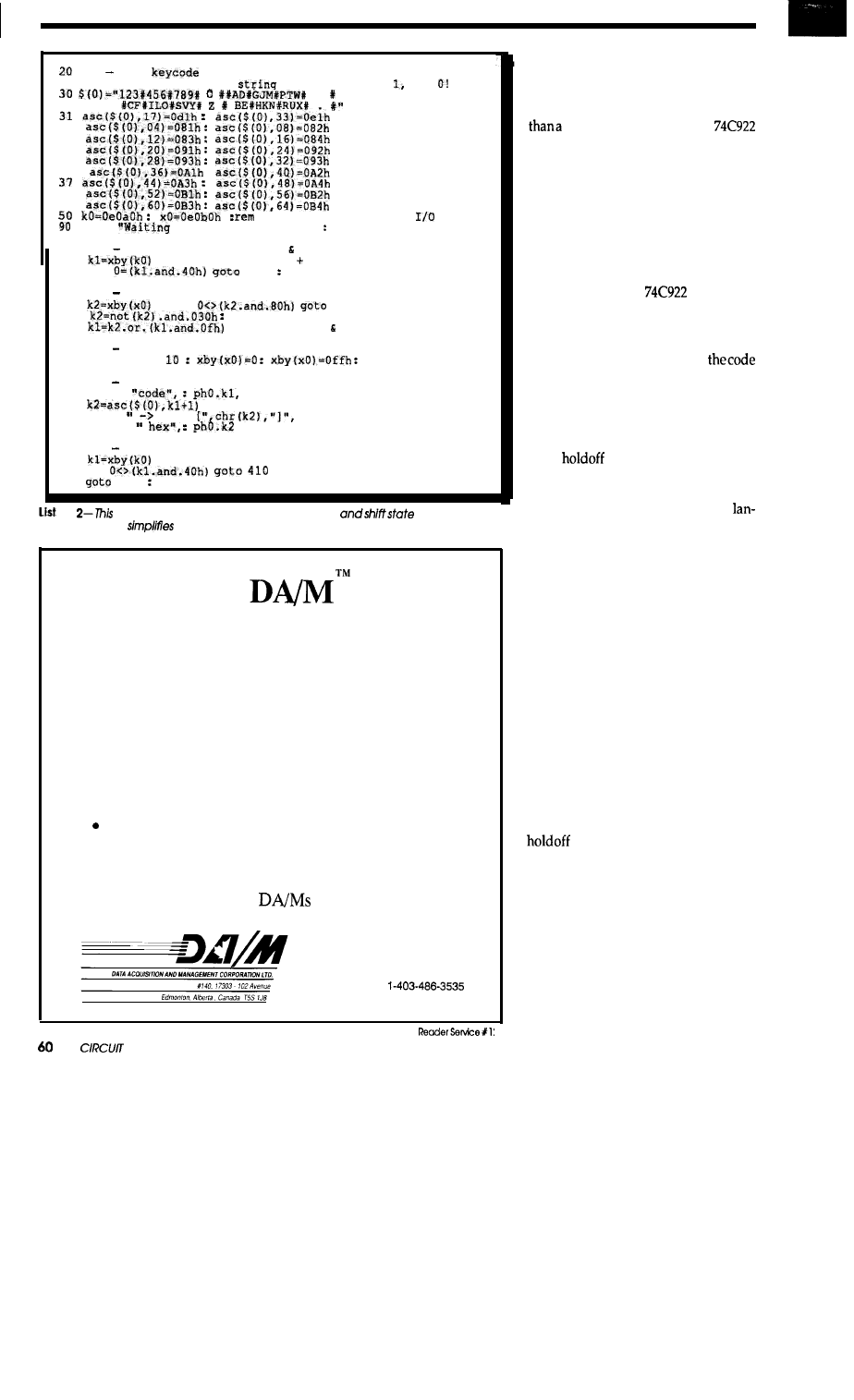
r e m
Set up
conversion table
22 string 66,134
: rem the
index starts at not
Q
32
33
34
35
36
:
38
39
keyboard and parallel
addrs
for keypad input..." print
100 rem wait for keys to arrive display what we qet
110
: rem
fetch key code strobe bit
120 if
110
rem spin
if strobe off
130 rem wait for shift scan. then combine with key code
140
: if
140
150
rem
flip shift bits
160
: rem combine strip strobe
200 rem sound a tone
210
for
i=l to
next i
300 rem display the result
310 print
320
330 print
char
340 print
400
rem
wait for key release
410
420 if
500
100
rem do it again...
ing
BASIC-52program combines the key code
into a single byte.
A
lookup
table
the conversion.
The
The Lowest Cost Data Acquisition System
Our DA/M can solve more of your data acquisition
problems at a lower price than any other product on the
market. DA/M’s are used for:
l
Military meteorological stations,
l
Building management.
l
Automated hydroponic farming,
l
Industrial process control.
Your application
In fact, DA/M’s can be used whenever you can’t afford
to use any one else’s product.
Made in North America,
are available NOW!
Phone
l-403-486-3534
Fax
CELLAR INK
accomplish, but the logic is fairly easy
to understand.
Most “real” keyboards repeat a
key when it’s held down for more
fractionof a second. The
provides a single STROBE output
when a key is first pressed, so any
repetitions must be done entirely in
firmware. However, we can tailor the
initial delay (“holdoff”), as well as the
repetition rate, to the application at
hand by tweaking a few code con-
stants.
Because the code can’t read the
shift keys until the
scans their
column, the only “repeatable” shifted
keys are in the left column (which is
wired to the shift keys). The numeric
pad keyscan’trepeatbecause
doesn’t know if the keys should be
shifted before repeating them. This
isn’t a problem in my application, but
if all your keys must repeat in all shift
states you need a different keypad. I’ll
build
and repeat into the code
so you can see how it’s done, but
remember the design limitations.
Another reason for assembly
guageis traditional: speed. While most
programs don’t need blinding con-
sole I/O speed, spending too much
time in “spin loops” waiting for the
console to disgorge a new character is
a Bad Thing because it may prevent
the program from monitoring other
inputs. The keypad hardware may
require a few loops, such as the one
that picks up the shift bits after the key
is released, but using assembly code
can cut those delays to the bare mini-
mum.
Predictable timing means the code
must use one of the on-chip hardware
timers to generate regular interrupts.
Because the BASIC-52 interpreter uses
Timer 0 to count 5-millisecond inter-
vals, it makes sense to measure key
and repeat durations in mul-
tiples of 5 ms. Even if you’re not using
BASIC (and the demo routines for this
column don’t), it provides a conven-
ient “standard” to follow. And, of
course, timer interrupt routines had
best use assembly language.
In short, while the BASIC code
works, things go better with assem-
bler.
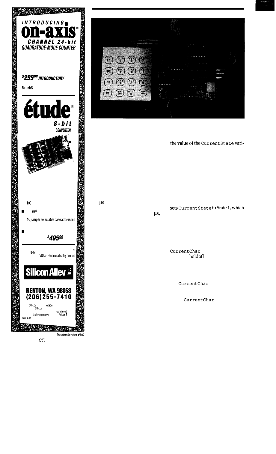
4
Acquires and displays position infor-
mation from optical encoders. Resolu-
tion is four times the encoder. Com-
plete with demo software and driver
source code.
PRICE
(add $150 for optional connector to
Lomb “glass scales”.)
25 MHz
ANALOG-TO-DIGITAL
Based on the TRW THC1068 hybrid
flash converter, its high signal-to-noise
ratio yields excellent accuracy at the
Nyquist limit.
n
4 KS of cache SRAM or to host as
converted at DMA speed
n
or DMA data transfer
n
10 MHz full-power bandwidth
3.92
resolution
n
Factory calibrated
n
n
External clock and trigger inputs
TTL compatible
Software source code included
P R I C E :
Each product requires: PC compatible
length
expansion slot. DOS 2.11 or
greater. EGA,
for graphic representation of data.
P.O. BOX 59593
01990
Alley Inc.
and
on-axis are
trademarkof
Alley Inc. Other brand or prod-
uct names are trademarks or
trade-
marks of
holders
spew
subject to change.
Photo 2-A combination of left and right shift keys plus function
keys
makes for a very
powerful keyboard-like keypad.
KEYED STATES
because the keypad interfacedoes
not use interrupts, the code must poll
it to detect new keys. Most application
programs cannot poll often enough to
catch every key, so this task is best left
to an interrupt routine. The timer ticks
every 5 milliseconds, so it calls the
keypad polling routine 200 times a
second.
The timer interrupt handler uses
110 every 5 ms, or 2.2% of the total
CPU cycles. Updating the clock and
handler overhead account for42 so
keypad polling requires 1.3% of the
CPU horsepower. That’s the tradeoff
for not lashing the application pro-
gram directly to the keyboard!
The keypad code cannot stall
while waiting for a key release, so it
must remember information between
interrupts. The classic solution is a
state machine that executes a specific
section of code for each value of a state
variable. The code changes the state
variable in response to external condi-
tions, like a new key press or a delay
expiring. In general, each state contin-
ues unchanged until an event occurs;
various events trigger changes to dif-
ferent new states.
There are three states: waiting for
a new key, waiting for nonrepeating
key to release, and waiting to repeat a
key. These states are represented by
able. Listing 3 shows one way to im-
plement the branches using the 8051’s
indirect jump instruction.
The code at
STATE
0 checks to see
if there’s a new key down. The keypad
is idle most of the time, so the code
bails out immediately. When a key is
pressed, the code reads the shift key
port to decide if the key can be re-
peated. If the key can’t be repeated
(because COL4 is not active), the code
will wait for the key release and read
the shift keys before converting the
data.
However, if the key is repeatable,
the code reads the shift key data, con-
verts the hardware information to a
character, and loads the result into the
variable. It also sets
the initial
delay into a variable
and selects State 2, which will wait for
the delay to expire, load the repeat
delay, and set the output variable
again.
is the interface
between the application program and
the keypad firmware. The application
reads
and sets it to
zero; a zero means there was no char-
acter ready. The firmware loads new
characters as fast as they become
available.
62
CIRCUIT
/A R INK
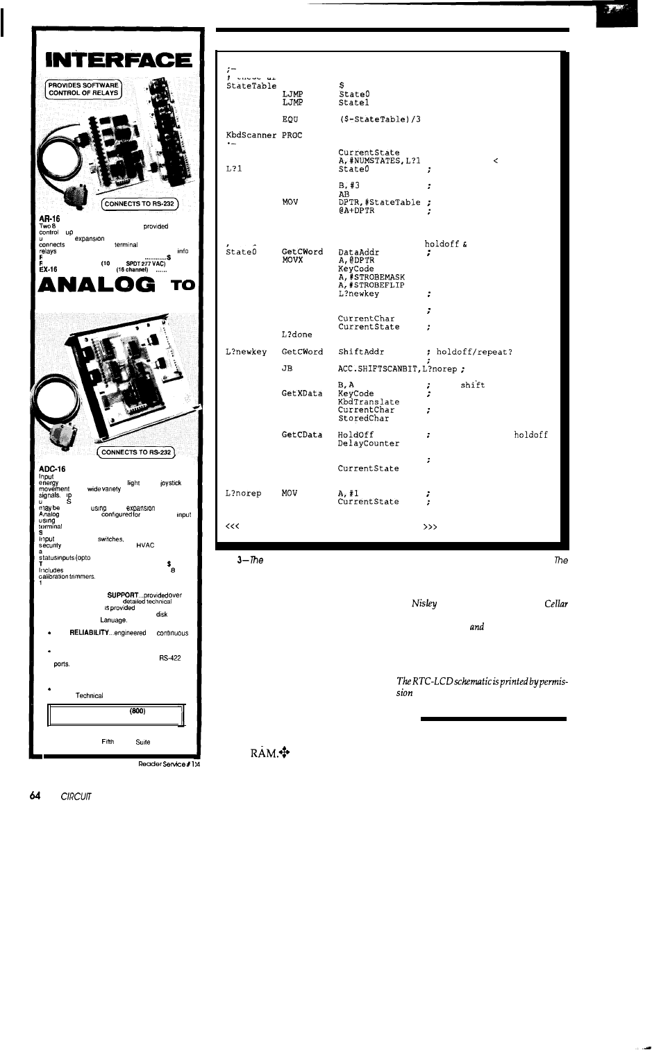
R E L A Y
RELAY INTERFACE
$ 89.95
channel relay output ports are
for
of
to 16 relays (expandable to 126 relays
sing EX-16
cards). Each relay output port
to a relay card or
block. A variety of
cards and relays are stocked. call for more
ID-6 REED RELAY CARD (8 relays)
49.95
lH-6 RELAY CARD
amp
$69.95
EXPANSION CARD
. .
$59.95
D I G I T A L
(16 channel)
$99.95
temperature, voltage, amperage, pressure,,
usage. energy demand,
levels,
and a
of other types of analog
In
sing the
uts may be expanded to 128 status inputs
T-32 expansion cards and up to 112 relays
controlled
EX-16
cards
inputs may be
temperature
the TE-6 temperature input card. (enclosure.
block and cable sold separately)
J-32 STATUS EXPANSION CARD
$ 7 9 . 9 5
on/off status of
thermostats, relays,
devices, smoke detectors,
equipment
nd hundreds of other devices. The ST-32 provides 32
Isolators sold separately).
‘ E - 6 T E M P E R A T U R E I N P U T C A R D
49.95
6 solid state temperature sensors and
Temperature range is minus 76 to
45 degrees F. Very accurate.
. FULL TECHNICAL
the
telephone by our staff. A
reference manual
with each order
including programming examples on
in Basic,
C and Assembly
HIGH
for
24 hour industrial applications.
Use with IBM and compatibles, Tandy. Apple and
most other computers with RS-232 or
All standard baud rates and protocols may
be used (50 to 19,200 baud) default is 9,600 baud
6 data bits, 2 stop bits, no parity.
Use our 600 number to order free Information
packet.
Information (614) 464.4470
24 HOUR ORDER LINE
642-7714
Visa-Mastercard-Ametican Express-COD
ELECTRONIC ENERGY CONTROL, INC.
360 South
Street,
604
Columbus. Ohio 43215
keyboard scanner state branch table
these are real jumps, not just addresses!
EQU
LJMP
state2
NUMSTATES
; # of state entries
branch to state machine routines
,
GetXData
; fetch state variable
CJNE
: C set if A NUMSTATES
JNC
flush on error
MOV
MUL
JMP
turn into table index
point to table base
and dive into the
routine
-- State
0:
key wasn't pressed, so check for new one
,
if shift scan is active,
we start
repeat
fetch code + strobe
PutXData
; save for later
ANL
; isolate strobe bit
XRL
; and make 1 = active
JNZ
if zero,
still no key
CLR
A
no key, flush char
PutXData
PutXData
in case of state error
JMP
MOVX
MOV
save
state
fetch code again
CALL
; make it a character
PutXData
set it in the output
PutXData
A,@DPTR
(get shift scan state)
hiqh=not scanned
set up initial
PutXData
MOV
A,#2
go to state 2,
PutXData
;
wait for repeat
JMP
L?done
go to state 1,
PutXData
wait for release
JMP
L?done
Code for states 1 and 2 is omitted
listing
timer interrupt handler calls the keyboard scanner routine every 5 ms.
keyboard code uses a state machine
to
remember information between calls.
The BBS files for this column in-
clude revised LCD code along with
new timer and keyboard routines.
Make
sure you don’t mix the versions,
since the old code doesn’t handle all
the new entry points. The EPROM
area holding the constants now in-
cludes keyboard and timer setup val-
ues.
Next time around, I’ll look at
measuring temperatures, keeping the
time of day, and storing data in non-
volatile
Ed
is a member of tke Circuit
INK engineering staff and enjoys making
gizmos do strange
wondrous things. He
is, by turns, a beekeeper, bicyclist, Registered
Professional Engineer, and amateur racon-
teur.
of Micromint Inc.
IRS
2 16 Very Useful
217 Moderately Useful
218 Not Useful
CELL.4 R INK
FROM
Creating a Nonvolatile
RAM Module
THE
BENCH
‘m sure you’ve had
your thought process
interrupted many times.
It’s an everyday occur-
rence and shouldn’t
destroy your concen-
tration. Take this morn-
ing for instance: was
working on a problem
when Mary’s voice
clashed with the tune
was humming. “Did you
get a chance to look at that new ZIF
socket?” she queried. “Yes, I did and it’s
too hard to open, unless you’ve long fin-
gernails. We discussed the problem fur-
ther and I was ready to resume my quest.
“Now where was I going” puzzled. For what seemed like
an eternity, I stood there, my mind doing a playback of the
events leading up to the present.
visualizea journey
along the neural highway within my head, speeding from
one neuron to the next, across each appropriate synapse.
“Let’s see..
a new
project... prototype... parts installa-
tion... not finished... why?.
SOLDER, yeah that’s it. I ran
out of solder!” My mind was partying over the accom-
plishment. It seems as though even the chemical
memory
of our minds can lose a bit from time to time.
Everyone has seen the message “MEMORY ERROR”
pop up on the computer’s video screen. This is usually fol-
lowed by glazed eyes, an immovable stare, and a jaw
which falls clear to the floor. Eventually, a push of the reset
button allows one to rewind and start over, but the conse-
quences are usually the permanent loss of some data. You
have to wonder, was this due to a device failure or a
program bug. Hardware types will probably feel at ease
blaming the problem on a program bug, while software
gurus
know
it’s a design flaw.
I consider memory the most important part of a sys-
tem. It continues to shrink in size and cost. I wish I had a
buck for every time I’ve heard, “(fill in your favorite
number
I’ll never need more than that!” I remem-
ber when that number was in bytes, now it’s kilobytesand
even
Most PCs use dynamic RAM for temporary storage,
but the faster machines are using static RAM for speeds
necessary in caching. I happen to prefer static RAM even
though it requires more room per bit than dynamic RAM.
It’s easier to use and requires less power. Unfortunately,
even though its name-static-suggests it can retain data
without power, that just ain’t so. Once power is removed,
static RAM forgets everything you taught it.
August/September
65
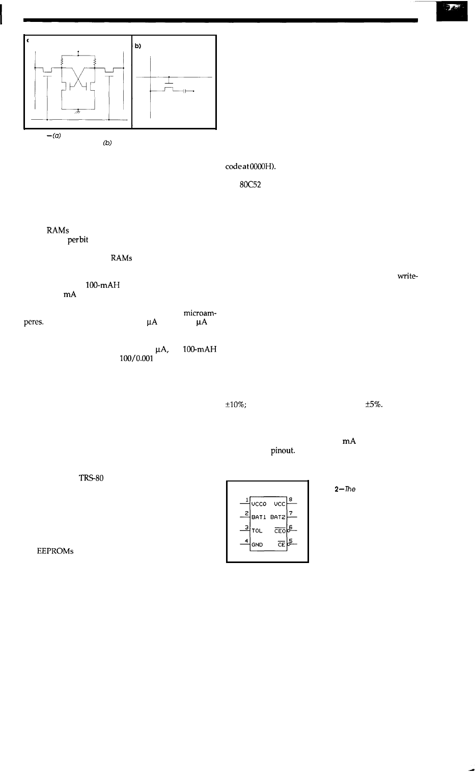
Figure
1
Static RAM cells are made up of transistors organized
in a flip-flop arrangement.
Dynamic RAM cells rely on charge
stored on a capacitor to retain data, so must be periodically re-
freshed.
TEMPORARY DATA RETENTION
Each cell or bit within a static RAM consists of a
number of transistors organized in a flip-flop arrangement
(see Figure la). Logiclevelsare set and held by the flip-flop
without having to recharge or refresh the cell, as in dy-
namic
(see Figure lb). This feature requires more
physical area
(a four-transistor
static
cell
has
roughly
four times the area of a one-transistor dynamic cell). You
can begin to see why static
are so much larger per bit
than dynamic RAM
S
.
Operating current for most static RAM is in the mil-
liampere range. A
battery could sustain a static
RAM at 10
for 10 hours-hardly worth considering.
However, static RAM does have a data retention mode in
which the current requirements are reduced to
This varies greatly from 100
down to 1
in
some cases. (Check data sheets carefully since not all
manufacturers produce these extremely low power ver-
sions.) At a data retention level of 1
the
battery will sustain life for
or 100,000 hours.
That’s over 4000 days or in excess of 11 years. Now we are
talk’n possibilities!
EXTENDED DATA RETENTION
EPROMs are an accepted (semipermanent) form of
data retention. Semipermanent not because they can be
erased, but because they rely on a memory cell which holds
a charge that eventually leaks off, losing the data. I don’t
mean to frighten anyone with this but someday your
computer will forget its own name-sort of like solid-state
Alzheimer’s disease. By that time, though, it will be collect-
ing dust like my
Mode1 I, so it really won’t matter.
Actually, at room temperature, a covered EPROM will
retain its charge for thousands of years. Left uncovered
under indoor fluorescent lights, it would take only three
years to lose its charge. Outdoors and exposed to the sun,
an EPROM could be erased in as little as a week. It is no
wonder that high-intensity UV erasers can pound those
electrons free in as little as ten minutes.
can give you a read/write version of an
EPROM using only 5V. They don’t require the higher
66
CIRCUIT CELLAR INK
programming
voltages
of EPROMs but are very expensive
and do require special write timings. This means they are
not a drop-in replacement for the read/write abilities of
today’s static RAM.
This leads us back to the static RAM for data retention.
Why all this talk of data retention? Many projects require
thecollectionand storageofdataevenafterthepowergoes
down. The loss of power may be deliberate, to save energy
when using batteries, or unexpected from an interruption
of line voltage. When the systemreturns to operation, your
data must be fully intact.
Program development is another area where data
retention can come in handy. Most microcontrollers start
executing code upon power-up (the 8031 starts executing
Many micros with a built-in high-level lan-
guage come up in a command mode, ready for user input
(the
executes BASIC). If the processor finds the nec-
essary information stored at a particular address, it will
automatically enter the execution mode and run the pro-
gram written in the high-level language. This auto-execu-
tion information, whether it be machine language or a
high-level code, is generally stored within an EPROM. A
battery-backed static RAM can serve as a replacement
device for the EPROM. This lets the user skip all the steps
involving Intel hex files, EPROM programmers, and ultra-
violet erasers. If using a read/write device as read-only
memory makes you cringe a bit, you can add a
protect tab to the RAM. No, it’s not a joke, although it is
more like 8” diskette protection. Remember those, where
you remove the tab (in our case a jumper) to protect the de-
vice from a write operation?
POWER-UP/DOWN PROTECTION
There are two main problems in protecting the con-
tents of static RAM during a power fluctuation. First,
whenever normal power is interrupted, Vcc of at least 2
volts must be maintained on the static RAM. Second, write
protection must be maintained during times of insufficient
Vcc. Normal Vcc would be 4.5-5.5 volts, which is 5 volts
or 4.75-5.25 volts, which is 5 volts
Detecting
out-of-tolerance Vcc, protecting an unauthorized write at-
tempt, and switching over to battery back-up can be ac-
complished by one device: the Dallas DS1210.
The DS1210 requires only 100
for operation. See
Figure 2 for a
Pin 1 is Vcc output to the static RAM.
It will switch between system power and battery voltage
for data retention when system power is out of tolerance.
D S 1 2 1 0
Figure
Dallas Semiconduc-
tor DS 12 10 handles all the details of
switching from the regular power
supply to backup batteries in
the
event
of a power loss.
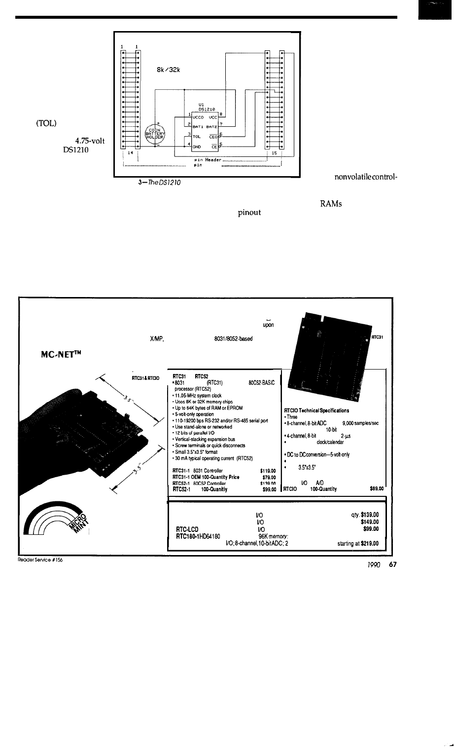
Pins 2 and 7 are inputs for
external batteries. The chip
will use whichever battery
is of a higher voltage, allow-
ing for replacement of the
batteries one at a time with-
out loss of memory. Only
one battery is necessary for
operation. The tolerance of
Vcc can be selected by tying
pin 3
high for less
than 4.5-volt detection or
low for less than
detection. The
uses
pin 4 for ground. Pin 5 is an
input for the static RAM’s
normal chip select. Pin 6 is
the protected chip select
output to the static RAM.
28 28
R A M
. . 28
28
Socket
Figure
makes constructing
a battery backed u p
socket for
RAM
chips
easy.
The rerouting of the RAM’s normal chip select signal
through the DS1210 allows illegal chip selects to be dis-
carded, thereby protecting the data held within the static
RAM. Pin 8 provides system power to the DS1210. It is this
pin which will be monitored for an out-of-tolerance condi-
tion.
In addition to these functions, the DS1210 can alert the
system to a low-battery condition. This is accomplished by
doinganondestructive testonanymemoryaddresswithin
the static RAM immediately after a power-up. Read a
location and save this value
for
replacement later.
Write
some other value (the
value’s complement is a
good choice) and try to read
it back. If the write/read
compares, then the battery
is OK. If not, then the
DS1210 will block chip se-
lect during the read opera-
tion and the value read back
will not match. The read
control is only affected
once-on the second read
after power-up.
See Figure 3 for a
quickie
ler. I chose to make a few
additions which allow the
module to work with 8K and 32K
and let the RAM
module
directly resemble an 8K or 32K EPROM.
This allows the RAM module to be loaded with code from
a read/write space and moved to a ROM socket totally
protected from accidental writes (see Figures 4 and 5).
DANGER-CONSTRUCTION AREA
If you are planning to build the simple nonvolatile
RAM module, you will need the parts
shown
in Table 1.
MICROMINT Introduces “Micro” Controlling!
After years of experience in manufacturing OEM controller boards and talking to customers, we think we have hit
just the right combination of format and function to satisfy even the toughest case of ‘relay mentality.” Realizing that
not every computer/controller application warrants a Cray
Micromint offers a tiny
controller
board for those dedicated and cost-sensitive installations.
New
software links your desktop up to 31 RTC controllers.
STACKED
I
and
Technical Specifications
processor
or
Micromint
bidirectional parallel ports (24 bits)
(D-W);
(optional &channel,
ADC)
DAC (D-W);
response time
Battery-backed
and presettable
time-interrupted capability
operation
Screw terminals or quick disconnects
Small
format
OEM
Price
RTCIO RTCIO board with parallel
and
convener
$1 i9.M
OEM
Price
MICROMINT, INC.
Also Available
RTC-OPT0 B-channel Optoisolated Expansion Board
single
RTC-SIR Serial, Timer, and Infrared Expansion Board
single qty.
LCD, Keyboard, and X-10 Expansion Board
single qty.
Controller Board.
1024 bits EEPROM;
4
Park Street, Vernon, CT 06066
Tel:
(203)
871-6170
l
F a x :
(
2
0
3
)
8
7
2
-
2
2
0
4
24 bits
TTL
serial ports
August/September
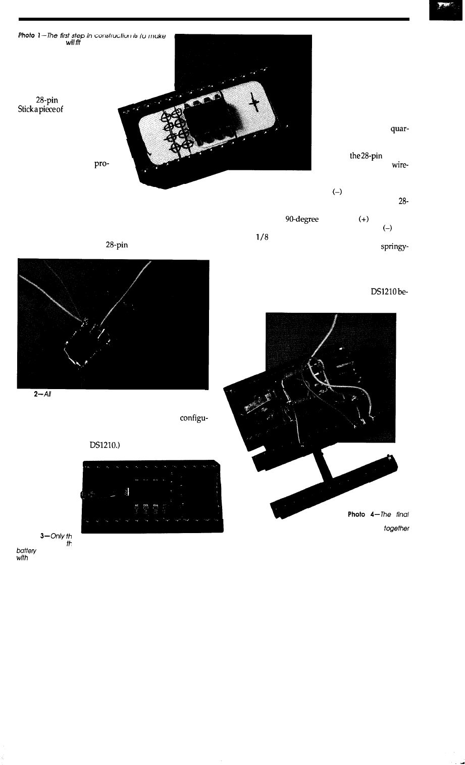
sure everything on the header.
[Author’s Note: Please review this proce-
dure completely prior to any assembly. Place the
various parts upon one another to help visualize
how fhings should fit.1
Construction begins
with
header/plug.
masking tape
between the pins on the
header and mark the eight
spots where the square pin
headerwillbemountedinto
the pin-l end of the header.
The pins should not
trude past the end of the
header.
Since the coin battery
holder is too large to fit into the header, remove the con-
tacts from the holder. Mark the mounting positions for the
battery contacts on the masking tape at the opposite end of
the header. Check to verify the DS1210 will fit between the
right-angle pin-header and the coin battery contact before
putting any holes into the
header. See Photo 1.
Photo
the
socket configuration is accomplished through
four 2-pin jumper headers.
(If you choose to wire the header without the
ration jumpers, you may wish to add a second coin battery
for double the backup capacity. Wire each battery to its
own input pin on the
The holes can be either
drilled, if you have access
to small bits, or melted by
using a paper clip or other
appropriately sized piece of
metal. I used a piece of wire
wound around my solder-
ing iron’s tip.
Prepare the right-angle
configuration header using
wire-wrap wire and
ter-wattresistors.SeePhoto
2. Superglue the right-angle
pins into
header.
Next, solder a
piece of
wrap wire to each of the
coin
battery
contacts.
Insert
the contact of the bat-
tery holder (the center one that looks like a nail) into the
pin header and bend over the stem on the bottom of the
header. Put an extra
bend in the
contact (the
long contact which holds the battery against the con-
tact) about
inch below the prebent comer forming a
“C.” This part is made of hardened steel to hold its
ness, so don’t ruin your favorite cutters when trimming the
excess leads on the bottom of the header. Trim the leads to
prevent the battery contacts from shorting to one another.
Now trim the ends off each pin of the DS1210 so that
it will lay flat on the header. Superglue the
P h o t o
spring clip from
holder is
USE
the final socket
68
CIRCUIT CELLAR INK
step of connecting
everything
is by far the trickiest.
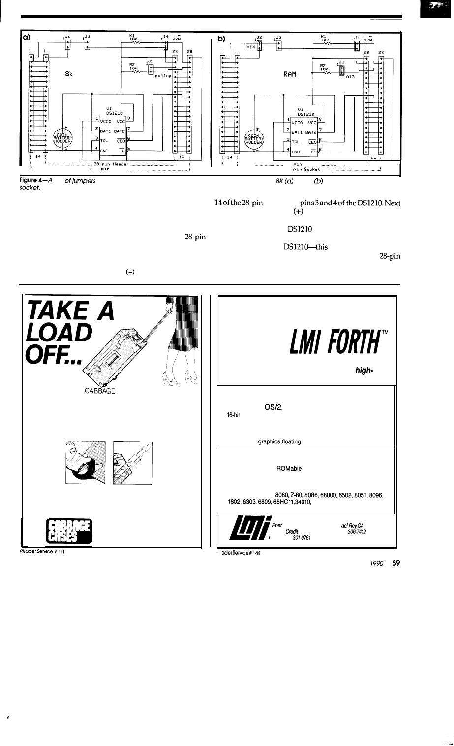
as RAM
32k
as
2 8
H e a d e r
2 8
. . . . . . .
2 8
S o c k e t
Pair
on
the basic battery backed up socket allow the use of either
or
32K
RAM
devices on the same
tween the right-angle header and coin battery contacts.
Use a bit of glue to help hold the battery contacts in place.
See Photo 3.
If you refer to the schematic, you will see that most of
the IC socket’s leads will connect directly to the
header. However, five out of the 28 pins will not make
direct connections. These five connections are interrupted
by the configuration jumpers and battery back-up control.
First solder the ground from the battery contact to pin
headerand
solder the wire from the battery contact to pins 2 and 7
of the DS1210. Now solder one lead from the pull-up
resistors to pin 8 of the
and the other lead to pin 28
of the 28-pin header. Solder a wire from pin 20 of the 28-pin
header to pin 5 of the
is the CE input. Solder
the appropriate wires to pins 1, 26, and 27 of the
header all coming from the right-angle configuration
header.
A rugged
CASE? lined with
plenty of foam for your equipment can
TAKE A LOAD OFF YOUR MIND
when you’ve got to travel.
TAKE A LOAD OFF YOUR BACK
with our exclusive tilt-wheels
and extension handle option.
UNLOAD ON US!
Call or write to tell us about your
shipping or carrying problems
WE HAVE SOLUTIONS!
CABBAGE CASES, INC.
1166-C STEELWOOD ROAD
COLUMBUS, OHIO 43212-1356
(614) 486-2495 FAX (614) 486-2788
(800) 888-2495
Total control
with
For
Programming Professionals:
an expanding family of compatible,
performance compilers for microcomputers
For Development:
Interactive Forth-83 Interpreter/Compilers
for MS-DOS,
and the 80386
l
and 32-bit implementations
l
Full
screen editor and assembler
l
Uses standard operating system files
l
500 page manual written in plain English
l
Support for
point, native code generation
For Applicatioris: Forth-83 Metacompiler
l
Unique table-driven multi-pass Forth compiler
l
Compiles compact
or disk-based applications
l
Excellent error handling
l
Produces headerless code, compiles from intermediate states,
and performs conditional compilation
l
Cross-compiles to
V25, RTX-2000
l
No license fee or royalty for compiled applications
Laboratory Microsystems Incorporated
Office Box 10430, Marina
90295
Phone
Card Orders to: (213)
FAX: (213)
August/September
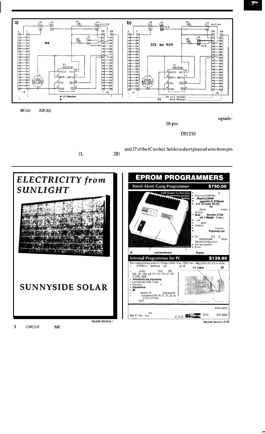
8k
R O B
............................. ........ 28
.....................................
.................................................
28 in Socket .................................................
Figure
5-A second pair ofjumpers allows the developer to write-protect the RAM in the socket allowing it to look like a ROM.
both
and
parts are supported.
Again.
Dress the wiring away from any pins to prevent shorts
which may be caused by the melting of insulation when
the pins are heated. There will not be much room between
the IC socket and the 2%pin header, so keeping the wiring
short will help to ease assembly.
Remove both of the end
cross
pieces from the IC socket
so that the two sides are held together only by the center
cross member. Bend the five pins 20, 26, 27, and
inward so that they will not make contact with the 28-pin
header when the two are mated together. Lay it
down and next to the
header, so that pins 15-28 of
each device are next one another. See Photo 4. Solder a
short wire from pin 6 of the
to pin 20 of the IC
socket-this is the CE output control. Solder the two
appropriate wires from the right-angle header to pins 26
1 of the DS1210 to pin 28 of the IC socket-this is the
switched Vcc source which will power the RAM. One wire
Photovoltaics for remote and online power
applications. Reliable, renewable electricity
from sunlight. Where there is a battery to be
charged, there is a place for photovoltaics.
RD4 Box 808 Green River Road
Brattleboro, Vermont 05301
802-257-1482
or circle
172 on the Reader Service Card
Completely stand-alone
PC driven
1
User
Parallel In and
32K
Flash EEPROM
upgrades
Pulse
in
5
in
2
warranty
Made A
support by phone
Complete manual and
Single
Sock.91
available. $550.00
and Shuffle 32
100
Macros.
Intel Hex. and Motorola S
Key
Tactile
Keypad
20 x4 Line LCD
2 Meg
5
card
external40
40 pin
Reads.
and programs
32.
64.
68764.2532
voltage
Hex, and Motorola formats
32 Meg EPROMs
personality modules required
1 year
day money
Adapters
TMS 7742,
and memory cards
Made A
NEEDHAM’S ELECTRONICS
Call for more
4539 Orange Grove
-Sacramento. CA 95841
(916)
924-8037
PST
CELLAR
Quan
Vendor
Description
Digi-Key
12mm Coin Cell Holder
Digi-Key
l(2)
28HP
Coin Battery (38
Jameco
28-pin Header Plug
1
DS1210
Dallas Semi
Power Monitor
1
24-pin Socket
(open-body construction)
Add these items for the universal version RAM/ROM module:
even with the low-powered RAM installed,
although, if you use only one battery, the data
will be lost when the battery is removed.
UP TO YOU
923872R
Jameco
Jameco
Jameco
2x4 R-Angle Sqr-Pin Header
(available in snap-off strips)
Shorting jumpers
5% Resistors
Select the device type as RAM and the ap-
propriate device size
Insert the
module into your favorite system’s static RAM
space and fill the contents of the RAM with
code or data. The device can now provide
battery-backed storage for your data-logging
Table l-All
of the parts necessary to
make your
own battery-backed RAM
application or can be reconfigured as ROM
(write protected) and inserted into a ROM
socket are readily available.
remains from the right-angle configuration header. To
keep the leads short (remember, all this has to be crammed
between the sockets), rotate the IC socket atop the 28-pin
header before soldering it to pin 1 of the IC socket.
Recheck connections and dress wiring away from the
28-pin header’s pins because you probably won’t get a
second chance at this step once the IC socket’s pins are
completely
soldered. Place the IC socket
firmly atop
pin header matching the IC socket’s pins with the header’s
pins. Start by soldering two pins on each side of the assem-
bly. Make adjustments in the alignment of the socket and
header by reheating the four connections until everything
looks good. Verify that the five connections (pins
27, and
on the socket and header will not be shorting.
If all is well, solder the remaining connections all the way
around the socket/header assembly.
Insert the appropriate shorting jumpers on the con-
figuration header. Cut a small piece (0.1 x 1 inch) of Mylar
(or other insulator) and insert it into the battery holder,
forming a “C”-shaped wall. This will prevent the coin
battery from shorting to one (or more) of the header/
socket pins. The coin battery can be removed/inserted
S O U R C E S
Corp.
Jameco Electronics
701 Brooks Ave. South
677
Rd.
Thief River Falls, MN
Belmont, CA 94002
592-8097
3444539
Dallas Semiconductor Cor
4350
Pkwy
Dallas, TX 75244-3219
(214) 4500400
The
is available from:
Circuit Cellar Incorporated
4 Park Street
Suite 12
Vernon, CT 06066
Send
(check or
money order)
socket
ROM emulation. I’ll bet a whole
slew of applications are popping into your head right
about now. I don’t know about you, but if I don’t write my
ideas down, they end up permanently in the bit
bucket..
means my battery needs changing.+
(pronounced
“BAH-key-AH-key”) is member of the
Circuit Cellar
His background includes
both
and manufacturingfields. In his spare
time,
enjoys
his family, windsurfing, and pizza.
IRS
2 19 Very Useful
220 Moderately Useful
221 Not Useful
FORTH DEVELOPMENT
The development
system consists of a
two-board set. The tar-
get board can be used in
a stand alone mode as a
sin
FO
e chip unit with a
TH kernel and
UD
to
32K byte
eprom and 2K ram or
with a piggy-back
memory expansion
board with either 64K
bytes
of 16
bit
or 3:2K bytes of_
a-bit ram
The
has two
serial ports, sockets for 8 buffer
two 40 pin
headers for
or expansion, and battery backup for both the
on the CPU and all of the expansion board ram.
The
sin
watchdog timer, 68 I
e chip 7700 famil has eight
timers, a
0 lines, two UAR
(synch or
hardware
multiply and divide, nineteen interrupts, and an
A-D converter
with an 8 channel multiplexer, all with a typical
They are available in both
and 16
wer dissipation of 30
versions and with
of on-chip
ram and up to 32K bytes of on-chip ROM
Also available is a very low cost ($125) prom programmer that
can be used with the development system to bum either
series of
EPROM’s or, with an adapter, the eprom version of the 7700 chips.
Full development systems with FORTH source code for as-
sembler, disassembler, editor, prom programmer and man other
utilities as well as a 6K FORTH kernel rom are available N W!
Target Board prices
start at
Package
prices and quantity
HORNE ELECTRONICS,
33122 181st. Ave. S.E.
counts available also.
Auburn, Wa. 98002
(206) 735-0790
August/September

Reader Service
Number
Advertiser
101
102
103
104
105
106
107
108
109
110
111
112
113
115
116
117
118
119
120
121
.
123
124
125
127
128
129
130
131
132
133
134
182
135
136
137
138
139
140
All Electronics
15
Alpha Products
4
Andratech
51
Annapolis Microsystems
33
A.T. Barrett Associates
86
Avocet
c 2
Aware Electronics
87
Binary Technologies
5 1
Designs
c 3
Byte Boss Intelligent Systems
87
Cabbage Cases
69
CAD Software, Inc.
23
Catenary Systems
43
Ciarcia Design Works
85
Ciarcia’s Circuit Cellar
72
Circuit Cellar
61
Circuit Cellar
61
Computer Doctors
2 1
Computerwise
11
Control Devices, Inc.
14
Cottage Resources
32
Covox Inc.
80
Deus Ex
Engineering
86
Industrial (DA/M)
60
Electronic Energy Control
64
Emerald Microware
7
Epoch Data
86
Express Circuits
45
F&W Communications
59
Gott Electronics
52
Grammar Engine
72
GTEK
c 4
Company
87
Hazelwood
10
High Res Technologies
87
Equipment Corp.
47
Horne Electronics, Inc.
71
lnfinico
30
Information Modes
86
lnnotec
14
Integrated Vessel
16
Corp
37
Kelvin Electronics
87
Page
Number
C
IRCUIT
C
ELLAR
I N K
ADVERTISER’S INDEX
141
142
143
144
145
146
147
148
149
150
151
152
153
154
155
156
122
157
158
159
160
161
162
163
164
165
166
167
168
169
170
171
172
173
174
175
177
178
179
180
181
Kelvin Electronics
87
Komputerwerk
86
Herb
(R. Fringe Publishers)
16
Laboratory Microsystems
69
Link Computer Graphics
63
Logical Systems
80
Louis E. Wheeler
87
Master Voice
27
Meredith Instruments
11
Merrimack Valley Systems
11
Corporation
50
Micro Dialects, Inc.
8 1
Micro Digital
78
Micromint
17
Micromint
33
Micromint
67
Micromint
77
Micro Resources
78
Ming Engineering (Electronics 1 2 3)
16
Needham’s Electronics
70
Inc.
22
Nisley Micro Engineering
86
NOHAU Corp
6
Paradigm Systems
63
Parallax, Inc.
42
PC Boards
6
49
R4 Systems
87
Real
Devices
20
Silicon Alley
62
Softools
25
Software Success
87
Sunnyside Solar
70
Synetic Systems
58
Tanner Electronics
33
39
Tinney
39
Traxel Laboratories, Inc.
15
Universal Cross Assemblers
77
Unkel Software, Inc.
55
URDA, Inc.
86
Velotec
86
Associates
86
SUBSCRIPTION PROBLEMS?
you
OR
of
OR
ON
I N K
AT
( 2 1 5 )
OR
Cincuir
INK
D
EPARTMENT
P.O. Box
PA 19398
1
IRS
INK Rating Service
How useful Is this article?
At the end of each article and some features there are
digit numbers
by which you can rate the article or feature.
Please take
time to let us, at Circuit Cellar INK, know how
you
our
material rates
you. Just circle the numbers
on the
card.
August/September 1990
7 3
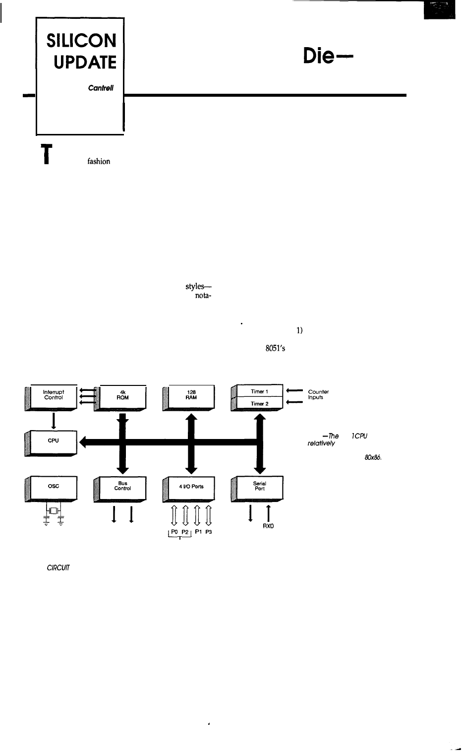
Old 8051s Never
Tom
They Just Get Smarter
New Power for a Controller Mainstay
he world of
is
known for styles that change?
with the season (stock market? phases of the moon?).
Change, whether worthwhile or gratuitous, is what drives
consumers to trash last year’s perfectly good outfits in
favor of new. Despite rational pretensions, it seems like the
world of high-tech gets equally
dizzy
over
the latest fad. A
voracious pack of headline-hungry trade press descend on
the premier high-tech shows (Comdex, ISSCC, etc.) to
report the latest trends (“Cycle Times Are Down, But Tiny
Instruction Sets Put Pipelines On Display”).
Detect a bit of cynicism? You can confirm it by taking
a look in my closet. For office work there’s the standard
selection of red-white-blue office gear-ties and lapels all
of medium width and nary a double-breast or sharkskin in
site. Otherwise it’s a nondescript mix of casual
jeans, T-shirts, sneakers-most notable for its lack of
bili ty. In the back of the closet you can see the clo thes I wore
in college-1 still like them and will wear them again when
I shrink. I never throw any clothes out, though the most
decrepit (I prefer “broken in”) sometimes seem to disap-
pear of their own volition. I suspect my wife must have a
External
Interrupts
1 1
hand in it-oil-stained
Apple
sweatshirts
with ripped-off
(unevenly, of course) sleeves may stand up by them-
selves, and even crawl, but they don’t just disappear.
Needless to say, my taste in micros also leans to-
ward the tried and true. Sure, I follow the news about the
latest in high silicon couture--but when it comes to
choosing my own “dailyware” I pretty much stick to the
basics. Take the 8051 for example, a micro that is been
around for a long time. Is it destined for the ash-heap of
micro history or, like a good pair of jeans,does it get better
with age?
MICRO
101
Before describing some of the latest developments
in the 8051 world, I’ll bring our younger readers (or those
who have been on another planet for the last 10 years) up
to speed with a short but sweet description of the de-
vice..
The 8051 (Figure was designed as a follow-on to
the world’s first single-chipmicro, the8048 Compared to
the 8048, the
main advantages are more complex
(complete?) instruction set, greater external expandabil-
ity (memory and I/O chips), and additional on-chip I/O.
CPU
T T
Figure
1
805
architecture
is
straightforward when
compared to Intel’s other famous
micros, the 8080 and
T X D
Address/Data
74
CELLAR INK
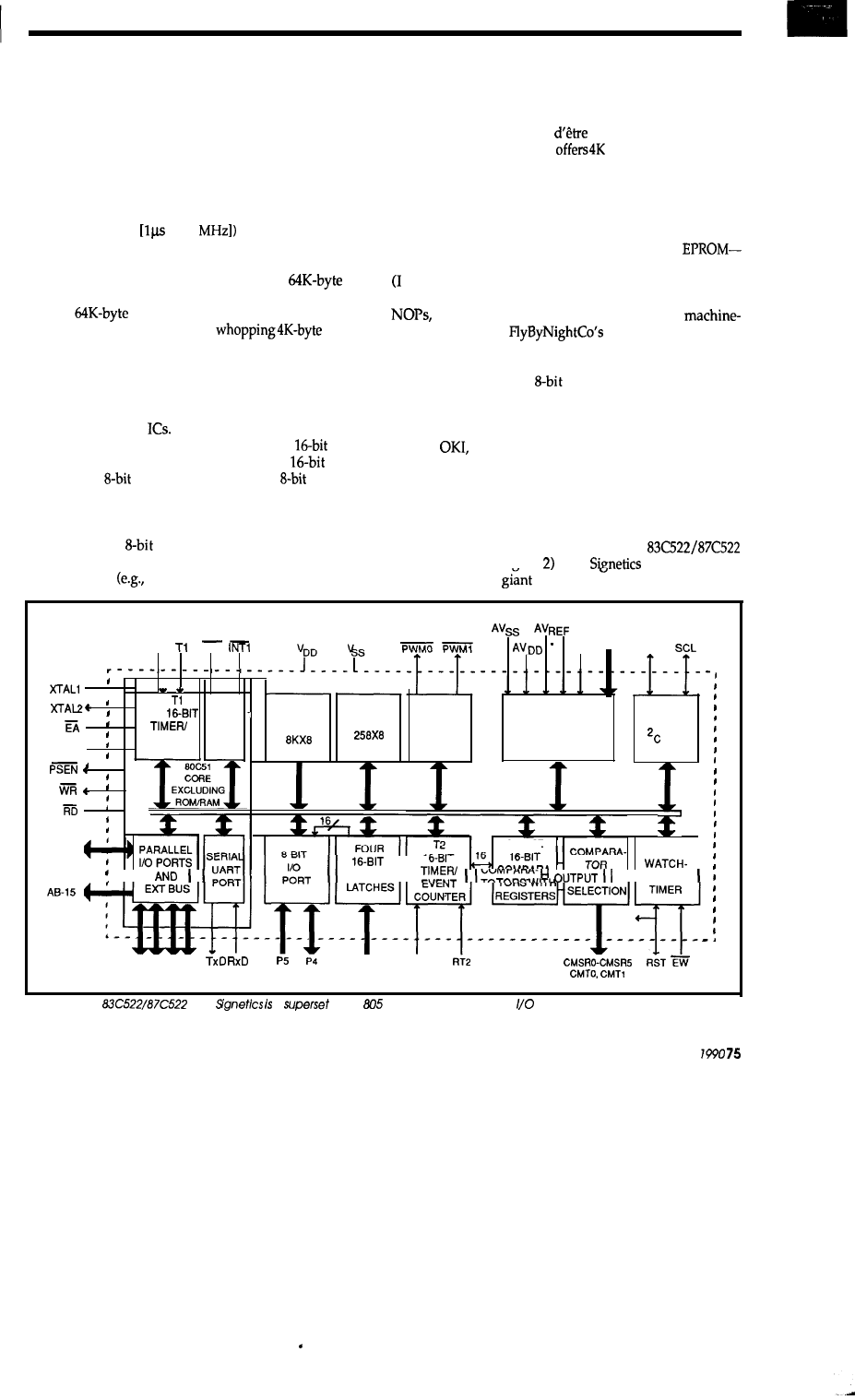
Without getting into the gory details, I’ll just say the
8051 CPUarchitecture-instruction set, registers, address-
ing modes, etc.-is relatively straightforward when com-
pared to Intel’s other famous micros, the 8080 and 80x86.
In contrast to these, and other non-single-chip micropro-
cessors, the 8051 is slightly less suitable for multichip, data
processing oriented systems and is better suited to effi-
ciently managing bit/byte-oriented control tasks. Notable
advantages for the 8051 include tight instruction encoding
(most instructions are one or two bytes long
and
execute in
one machine cycle at 12
and quick and easy bit
handling operations (set, clear, test, etc.).
For larger applications, the 8051 offers external
memory and I/O expansion via separate
code
and data spaces (designers often map them to a single
unified
code and data space). This is a big plus
over the 8048 which features a
external
address space. The single-chip orientation of the 8051
shows in the expansion bus; you won’t find big-system
features like DMA, vectored interrupts, DRAM refresh, or
wait-state capability. Nevertheless, the 8051 can easily
connect to the typical small-system mix of peripheral and
byte-wide memory
On-chip I/O-wise the 8051 offers two
timer/
counters (they can be configured as one
timer/
counter, one
timer/counter, and one
timer) and
a full-duplex UART. These modules are pretty basic, but
many applications don’t need a lot of bells and whistles.
Also, the chip offers a total of 32 bits of parallel I/O (four
bit-addressable
ports&just remember that the pins
are shared with other functions. Using the expansion bus
consume 24 of the 32 lines. Five interrupt sources (the
timers, UART, and two external interrupt request lines)
are serviced with a two-level programmable priority
scheme.
Of course, the raison
for a single-chip micro is
on-chip memory. The 8051
bytes of masked ROM
and 128 bytes of RAM. Since masked ROM is only cost
effective for highest-volume applications, two variants of
the 8051 are offered to help the small guy. The 8751
replaces the 4K bytes of ROM with EPROM-the ideal
solution, but expensive. Meanwhile, the 8031 deletes the
ROM altogether, requiring theuseof anexternal
a low-cost solution, but remember that I/O lines are lost.
suspect the 8031 actually has a ROM inside. I wonder
what the code is? Could be some bad ROM bits, endless
a factory test program-or perhaps the
readable legacy of
over-ambitious prod-
uct plans.)
To me, the biggest advantage of the 8051 family isn’t
really technical; many
micros can perform equally
well. The real virtue is that the 8051, developed in an era
with fewer lawsuits, has become a de-facto “people’s
micro.” The list of suppliers, besides Intel, includes AMD,
Harris,
Siemens, and Signetics. Multiple vendors
keep prices down and innovation up.
NEW TRICKS
Speaking of competition and innovation, let’s take a
look at a modern ‘51 family offering: the
(ROM/EPROM) (Figure from
(a subsidiarv of
and peripheral
UART, timer, and so on) I/O lines can Dutch electronics
Philips).
,
ALE
ADO-7
ADCO-7
TO
INTO
+ STADC
S D A
-
-
-
-
-
1’.
TO,
TWO
P R O G R A M
DATA
,
CPU
M E M O R Y
MEMORY
DUAL
SERIAL
PWM
ADC
EVENT
I
PORT
C O U N T E R S
ROM
RAM
8-BIT
INTERNAL BUS
THREE
I
T3
1
I
II
CAPTURE I I
D
O
G
P
O
pl P2 P3
C T 0 1 - C T 3 1 T 2
Figure
2-The
from
a
of the
1 offering such on-board
as ADC, PC port, and watchdog timer.
August/September
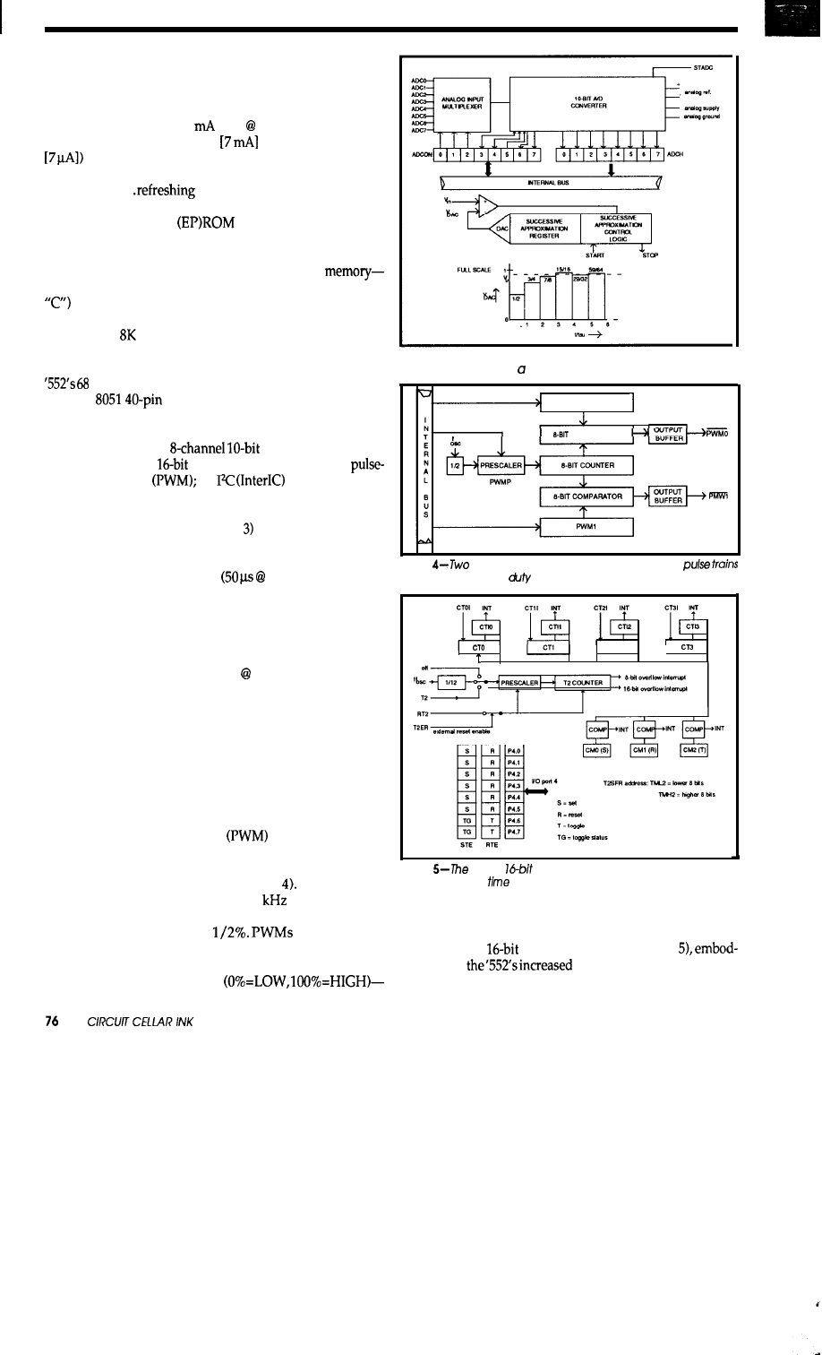
Of course, the “C” in the part number highlights one
dramatic change over the decade: the shift from NMOS to
CMOS. The ‘552, a much more powerful chip than the ‘51
as you’ll see, consumes one quarter of the power of the
older CPU (30mA vs. 125
max 12 MHz). Evenbetter,
‘552 low-power modes (IDLE
and POWER DOWN
can dramatically reduce average power consump-
tion. CMOS is another example of high-tech giving us
more for less..
isn’t it.
Another basic change is the doubling of on-chip
memory to 8K bytes
and 256 bytes of RAM.
Larger applications will be able to fit on-chip without
resorting to external memory. Presumably, future ver-
sions are on the drawing board with even more
increasing application complexity (and the hope to use
call for two, or even four, times as much. Neverthe-
less, a good assembly language programmer can do a heck
of a lot with bytes.
Don’t forget the packaging advances in the last few
years. The switch to high-density chip carriers packs the
pins
of functionality into less board space than the
original
DIP.
The I/O functions associated with the extra 28 pins
are what really separate the old from the new. These
upgrades include an
ADC; an additional,
and much smarter,
timer/counter; a 2-channel
width modulator
an
serial bus chan-
nel; and a watchdog timer. We’re talking serious system
integration here.
The A/D converter (Figure specs are pretty typi-
cal. Since it is a successive approximation type, conversion
(initiated by software or an external trigger) takes a rela-
tively long 50 machine cycles 12 MHz), but that’s
certainly fast enough for most mechanical control tasks.
The real advantage compared to an outside ADC IC is you
don’t have to resort to expanded bus mode (and lose a
bunch of I/O lines) to see if the water is boiling.
The watchdog timer works as expected. You pro-
gram a desired interval (2-510 ms 12 MHz, i.e., how long
your
system
can
remain crashed before the bits hit the fan).
Then you partition/schedule your software to reload the
watchdog within the specified interval. This can be tricky.
You have to account for all program paths, interrupts, and
so on. If the watchdog isn’t reloaded in time, it resets the
CPU (and can even drive the RESET pin as an output to
reset external chips). An external ENABLE WATCHDOG
pin and special timer reload protocol harden the watchdog
against inadvertent disability.
Pulse-width modulation
simply means gen-
erating a pulse train whose interval and duty cycle is
variable. Two independent channels, each with its own
pulse output pin, are provided (Figure The pulse fre-
quency can be set from 92 Hz to 23.5
at 12 MHz, with
the duty cycle variable between 0% and 100% with resolu-
tion (8 bits) of better than
are especially
useful for controlling DC motor speed, but you can also
use them to implement an integrating DAC. Otherwise,
use them as regular outputs
Figure J-The
successive approximation ADC on the ‘552 takes 50
machine cycles to do conversion.
P W M O
COMPARATOR
Figure
independent FWM channels generate
vhose intervals and
cycles are variable.
CT2
t
t
t ,
Figure
new T2
counter/timer makes it easy to keep
track of the real
between external events.
just the thing when the marketing department begs for an
extra LED at the last second.
The new
timer/counter, T2 (Figure
iesmuchof
functionality. Actually, the
timer/counter itself is much like the 8051’s original TO and
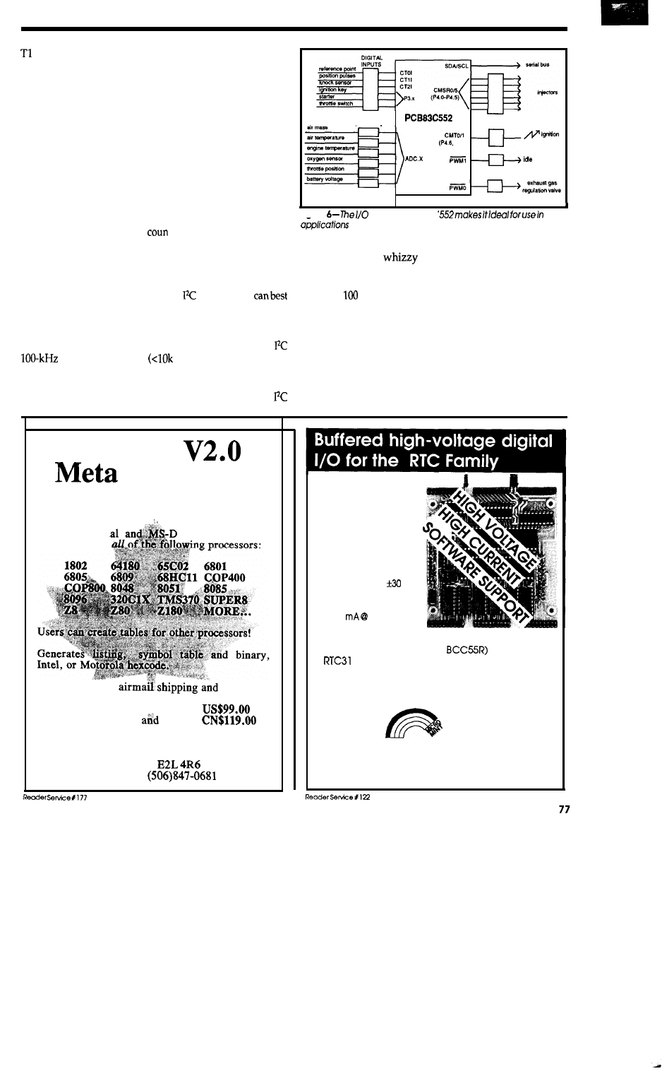
timers (also included on the ‘552). The only major
difference is that instead of being “loaded” by software, T2
can only be cleared by an external input. It’s the input
capture and output compare modules, supported with 12
I/O lines, surrounding T2 that add function. Four input
capture lines are provided. They are just like external
interrupt request lines, except a rising/falling edge (pro-
grammable) on any line also copies the T2 count to a
register associated with each line. Thus, it’s quick and easy
to keep track of the real time between external events: it’s
just the difference between counts in eachcapture register.
Meanwhile, eight output compare lines work in kind of an
opposite fashion. They generate output events (set/reset/
toggle) depending on the count in T2. Three registers are
compared with T2 on every
t and the preprogrammed
events are triggered when there is a match. Variable phase
shifting of the outputs is as easy as fiddling with the three
registers-ideal for an application like engine timing and
control (Figure 6).
The last major addition is the port, which
be described as a “LAN In A Box” (Figure 7). The idea of a
low-cost interchip serial bus is really neat. I expect it will
only grow in popularity. After all, why give up all your
valuable I/O lines just to add a chip or two. Sure, the
maximum bit rate
bytes/second consider-
ing protocol overhead) won’t get a second look from the
techno-gurus, but it is fast enough for lots of stuff and only
uses two wires (clock and data). In fact, the patented
ANALOG
SENSORS
P4.7)
valve
Figure
featuredon the
such
as an engine controller.
protocol is more
than it appears at first glance,
featuring multimaster arbitration, adaptive data rates
(accommodates fast and slow devices), and so on. Indeed,
it takes a or so lines of assembly language to drive the
port-fortunately the listings are in the ‘552 user manual.
HAPPY BIRTHDAY
Though the original 8051 is aging, the plethora of
suppliers ensure that innovation and specialization will
continue. Signetics offers half a dozen variants in addition
to the’552 described here-versions withon-chip EEPROM,
Cross-16
Assembler
Table based absolute cross-assembler using the
manufacturer’s assembly mnemonics.
Includes manu
OS assembler disk
with tables for
Free worldwide
handling.
Check, Money Order or P.O.
VISA, Mastercard
Canada
Universal Cross-Assemblers
POB 6158, Saint John, NB
Canada
Voice/Fax:
RTC-BUFIO
l
48
Digital I/O Lines
l
24 Digital Input Lines
(Capable of
withstanding
VDC)
l
24
Digital Output Lines
(Capable of sinking
250
50 VDC)
. 3.5’ x
3.8’
RTC
form-factor
l
BCC Bus-compatible (with
l
software supported with Micromint’s new
Threaded Programmable Controller Language
Priced at $99 (Single quantity)
MICROMINT, INC.
4
PARK STREET. VERNON, CT 06066
CALL TO ORDER l-800-635-3355
(203) 87 l-61 70
FAX: (203) 872-2204
August/September 1990
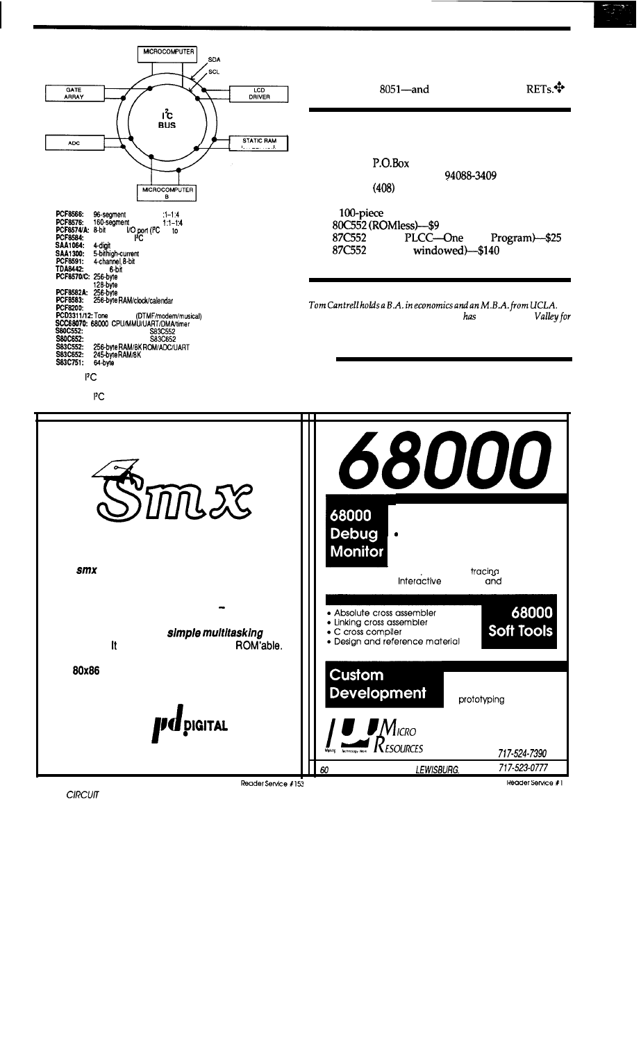
A
OR EEPROM
PCF9571:
LCD driver; 1
M
UX
LCD driver;
M
UX
remote
bus parallel converter)
B-bit parallel to converter
LED driver
driver
M
UX
; ADC + one DAC
Quad
DAC
static RAM
static RAM
EEPROM
Voice synthesizer (male/female speech)
generator
ROM-fess version of
ROM-fess version of
ROM
RAMRK ROM
Figure 7-The bus makes it easy to connect numerous devices
together using just two wires. A sample of the chips available
which support is shown above.
ones shrunk into 24-pin packages, and so on. Withal1 of the
suppliers proliferating parts madly, we’re facing a veri-
table baby boom of new ’51s. So, let’s celebrate the tenth
birthday of the
wish it many happy
Contact:
Signetics Corp.
811 E. Arques Ave.
3409
Sunnyvale, CA
991-2000
The
pricing for the ‘552:
(Plastic
Time
(Ceramic
(note: a lower cost package is being developed)
He
owns and operates Microfuture Inc., and
been in Silicon
ten years
involved in chip, board, and system design and marketing.
IRS
222 Very Useful
223 Moderately Useful
224 Not Useful
LEARN MULTITASKING
COLLEGE KIT $95
The
College Kit allows you to learn and to
experiment with multitasking. It includes demo
source code, a tutorial
User’s Guide, a
Reference Manual,
and help files everything
you need to try out multitasking! The CK is a
reduced version of our
executive.
runs at full speed and is
Use it with
MS-DOS
or stand-alone. Works with
the
family and
Microsoft
or
Turbo C
and
assembler. The full version of
smx
is available
for $1995 with no royalties.
MICRO
l-800-366-2491
CYPRESS, CA 906304630
. Suitable for embedded installation
l
Off-the-shelf for any hardware
Locate anywhere in memory
l
Full-feature memory and
register commands
l
Breakpoints and
.
assembly
disassembly
l
Design and reference material
l
Hardware and software
engineering design and
available.
.
or
SOUTH EIGHTH STREET
PA 17837
78
CELLAR INK
PRACTICAL
Getting to Know You
ALGORITHMS
Scott Robert
A New Feature Begins
W
hen inaugurating a new column, I always like
to introduce myself&d the “theme” I’ll be following. In
the former case, I’m the former C columnist for Micro Cor-
magazine--alas, now sadly defunct-and a
time writer. I focus on
writing
books and articles which are
helpful to programmers who are trying to
produce
reliable
and efficient programs.
Outside the world of computers, I’m backpacker,
amateur astronomer, photographer, and father to
old daughter Elora. I live in Gunnison Colorado, a
nity
of 6OOOpeoplelocated in thecentral Rocky Mountains.
Parts of these columns get written while resting in an
Aspen forest at 9000 feet above sea level. I’m not a radical
environmentalist, but I am involved in water issues and
conservation.
My computing environment is reasonably sophisti-
cated. I use a 20-MHz
computer, with a Mylex
motherboard, for my primary MS-DOS work. This com-
puter, known as Bull for arcane reasons, is equipped with
4
megabytes of memory, a 65-megabyte Mitsubishi MR535
hard drive,
VGA
color graphics, and
devices. I run MS-DOS 3.3 currently, since
isn’t quite compatible with everything.
In fact, this column is about the skill of the program-
mer. The focus is on algorithms, the step-by-step proce-
dures used to accomplish a programming task. A program
can bedefined as a large algorithm built from smaller algo-
rithms; the algorithms selected for a task will affect how
well the program’s task is accomplished. Like a good
mechanic, the programmer must know which algorithmic
tool to use to best solve a given problem. My goal is to help
you fill your toolbox with algorithms, and to show you
how to select those algorithms.
I’m well-known in some circles as a C and C++ pro-
grammer; my first two books are on C++, and I’m now
writing the C programming column for the magazine Tech
Specialist.
I’m not a language elitist, though. I happily
create software using
assembly language, Turbo
Pascal, Modula-2, and even FORTRAN. My philosophy is
that the language used to create a program is less impor-
tant than the skill of the programmer. C is not the best
language for teaching; its syntax can be very obtuse at
times, even for a C expert. C++
is also out; i t is my language
of choice, but is even more complex than its father, C.
Turbo Pascal is a structured language, but it is completely
nonportable outside of the MS-DOS world. FORTRAN is
old and klunky, and somewhat uncommon these days.
Modula-2 suddenly becomes the language of choice
for this column, It has a clear syntax, is available on many
platforms ranging from
to UNIX, and is
defined. I’ve seen Modula-2 used for every conceivable
project from sophisticated databases to embedded micro-
controllers. Designed by Niklaus Wirth as the successor to
his earlier programming language, Pascal, Modula-2 has a
“neater” syntax than Pascal and has extensions which
make it a powerful tool for the professional programmer.
Since the idea here is to present algorithms--and not
language-specific constructs-Modula-2 will do nicely.
If you don’t already use Modula-2, there are some
resources you can obtain. The language is defined by
Wirth’s book Programming in
printed by
ger-Verlag (ISBN 0-387-15078-l). There are several good
Modula-2 books on the market; you can look for these at
your local
bookstore. Modula-2 is a small lan-
guage, and many colleges and universities use it in their
programming classes. Academic book stores will proba-
bly have resources on Modula-2.
For MS-DOS, the best Modula-2 compiler is from
Stony Brook. It has a very fast and efficient code generator
which easily produces the fastest programs I’ve seen from
a high-level language. Also available for MS-DOS is the
Jensen and Partners’ Modula-2 compiler. There are one or
two Modula-2 compilers for
and I know that
Modula-2 compilers for embedded systems exist. If you
want a Modula-2 compiler, and don’t know where to find
one, drop me a note and I’ll try to help you out.
OPTIMIZING
Code optimizers are all the rage today. In essence, an
optimizing compiler attempts to produce the fastest pos-
sible program from the source code you give it. Nearly
every
compiler advertisement contains a list of benchmark
results, trying to prove that compiler A produces better
code than compiler B.
Don’t be taken by the hype; the best code optimizer
you have contains billions of interacting neurons and
resides in your head. An optimizer may improve code
August/September
79
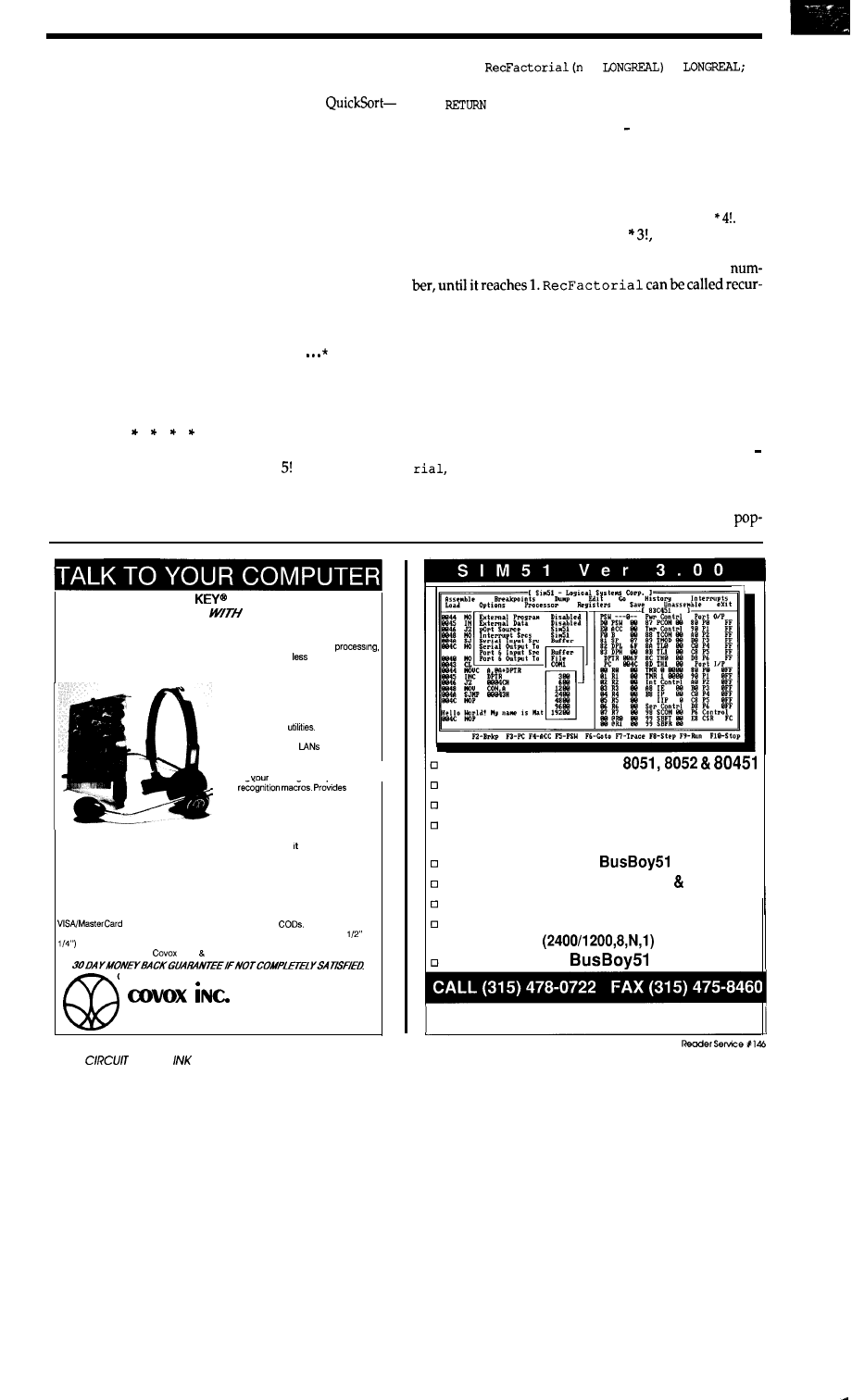
performance by 10 to twenty percent; your brain can
increase program performance by orders of magnitude.
No optimizer can convert a bubble sort into a
but your brain can. The algorithms you implement, and
the efficiency with which you program them, will deter-
mine the speed and size of your programs.
A case in point: Most programming texts will talk
about how recursion is the natural way of programming
certain algorithms. Recursion occurs when an algorithm is
defined in terms of itself. In programming terms, a recur-
sive algorithm is one in which a procedure calls itself in
stages to accomplish a task.
A factorial is a value which is used primarily in statis-
tics. The calculation of a factorial can be defined in terms of
recursion. The computation of the factorial for an integral
number takes this form:
factorial n = n * (n-l) * (n-2) *
2 * 1
In other words, a factorial is calculated
by
multiplying
together all of the integers less than or equal to the operand
and greater than or equal to one. The factorial of 5, for
example, is 5 4 3 2 1, or 120. The factorial of 1 is 1.
Usually, the exclamation point is used to indicate a facto-
rial calculation in mathematical texts; would mean the
factorial of 5.
The simplest implementation of a procedure to calcu-
late the factorial of a number would look like this:
PROCEDURE
:
:
BEGIN
IF n = 0.0 THEN
1.0
ELSE
RETURN n * RecFactorial(n 1
.O)
END
END RecFactorial;
A factorial for a number can be defined as multiplying
the number by the factorial of the number one less than it.
The factorial of 5, for instance, can be defined as 5 The
factorial of 4 can be defined a 4 and so on. So, a
recursive algorithm-like the one above-calls itself to
calculate the factorial of each successively smaller
sively because it is self-contained; the only variable it uses
is n, which is local to each call to RecFactorial. Proce-
dures which modify global variables cannot (in general) be
made recursive. The recursive calls end when n is 1;
RecFactorial
can at that point return a constant value
of 1 rather than calling itself further.
The recursive version of the factorial procedure is
clear and to the point-but is it efficient? The answer is no;
recursion involves making repeated function calls which
increase program overhead. For every call to
Re c F
a c t o
the value of
n
must be pushed onto the stack, along
with a return address, when the call is made. When an
invocation of
RecFactorial
is done, these values must
be popped off the stack. This pushing, calling, and
WITH VOICE MASTER
FOR PCs/COMPATIBLES
VOICE RECOGNITION
SPEECH RESPONSE
GIVE A NEW DIMENSION TO PERSONAL COMPUTING The amazing Voice
Master Key System adds voice recognition to just about any program or application.
Voice command up to 256 keyboard macros from within CAD, DTP, word
spread sheet, or game programs. Fully TSR and occupies
than 64K. Instant
response time and high recognition accuracy. A real productivity enhancer1
S P E E C H R E C O R D I N G S O F T W A R E
Digitally record your own speech. sound,
or music to put into your own software
programs. Software provides sampling rate
variations, graphics-based editing, and
data compression
Create software
sound files, voice memos, more. Send
voice mail through
or modem. A
superior speech/sound development tool.
INTERACTIVE SPEECH INPUT/OUT-
PUT Taa
own diaitized speech files to
voice
speech
response to your spoken commands -- all
from within your application software! Ideal
for business, presentation, education, or
entertainment programs you currently use.
Augment the system for wireless uses in robotics, factory process controls, home
automation. new products, etc. Voice Master Key System does all!
EVERYTHING INCLUDED Voice Master Key System consists of a plug-in card,
durable lightweight microphone headset, software. and manual. Card fits any
available slot. External ports consist of mic inputs and volume controlled output
sockets. High quality throughout, easy and fun to use.
ONLY
$149.95
COMPLETE
ORDER HOTLINE: (503) 342-1271 Monday-Friday 6 AM to 5 PM Pacific Time.
phone or FAX orders accepted. No
Personal checks
subject to 3 week shipping delay. Specify computer type and disk format (3
or 5
when ordering. Add 55 shipping charge for delivery in USA and Canada.
Foreign inquiries contact
for C F quotes.
CALL OR WRITE FOR FREE PRODUCT CATALOG.
675
CONGER ST.
TEL: (503) 342-i 271
EUGENE, OR 97402
FAX: (503) 342-i 283
80
CELLAR
Reader Service X121
Simulator/Debugger for
Full Screen, Menu driven
ALL registers ALWAYS displayed
Extensive Serial Port and ‘451 Port 6
support
In circuit debug with
probe
Debug all Memory models, Ext. Internal
Call or FAX for FREE demo version
Download demo (D51 DEMO.EXE) from BBS
(315) 475-3961
Only $250, with
$499
Logical Systems Corporation
P.O. Box
6184,
Syracuse NY
13217
USA
ping slows down
considerably.
heap because of poor design than any other reason.
call to it uses 12
bytes of stack space for
n
and the return
address. Most programs have a limited amount of stack
space. The more arguments a recursive function requires,
the more stack space it uses. Using
RecFactorial
to
calculate
will use 1200
stack space-clearly an
unacceptable amount for many applications.
In the next column, I’ll dive into sorting problems.
Every program sorts data, and it’s a time-consuming task
which requires the selection of the proper algorithm. I’ll be
showing you the oft-forgotten
algorithm, along
with an iterative version of the
algorithm that
runs 20% faster than the traditional recursive
A procedure for calculating a factorial can be written
without the use of recursion. For example..
WRAPPING UP
PROCEDURE IterFactorial(n LONGREAL) : LONGREAL;
result :
BEGIN
result := 1.0;
WHILE n 1.0 DO
result := result * n;
n := n 1.0
END;
RETURN result
END IterFactorial;
I like feedback from you; having contact with the
readers of my column was perhaps the best thing about
writing for Micro Cornucopia. Feel free to drop me a line at
the given address; please avoid calling me if you can,
because I get far too many calls already. Send me your
gripes, suggestions, and thoughts about where you want
this column to go. I can’t promise a response, but at least I
can tell you I’ll pay attention. After all, this column is
written for you, not me!
Until next time..
This function uses a simple loop to calculate a factorial.
Without recursion, this function
only
16 bytes of stack
space (for
n
and
result)
no matter which factorial is
being calculated. Lacking the overhead of multiple
Clearly, the better algorithm is the iterative one. An
additional benefit is that
performs one
thanRecFactorial,becauseitcanstopwhen
n
is reduced to 1. This eliminates an extra loop which
would multiply result by 1.
Scott
is a writer specializing in computer software. Correspon-
dence concerning “Practical Algorithms” may be sent to him at: Scott
West Virginia,
IRS
225 Very Useful
226 Moderately Useful
227 Not Useful
Any algorithm which can be defined using recursion
can also be defined using iteration. There’s a long mathe-
matical proof of this, but I’d prefer it if you’d just take my
word for it. I have yet to find an algorithm which is not
faster and smaller when defined iteratively as opposed to
recursively.
DESIGN VERSUS HACKING
I’m a believer in designing programs, as opposed to
building them on the fly. Many programmers from the old
“hacker” school (which I attended) prefer to build pro-
grams without doing
any
real design in the first place. This
has lead, in my view, to the current problem with code
bloat: Programs which perform poorly while using
ousamountsofmemory. Assoftwarecomplexityincreases,
programmers need to use more and more thought in how
their programs are designed.
EDITOR, CROSS ASSEMBLER, AND
COMMUNICATIONS FACILITY IN A COMPLETE
INTEGRATED DEVELOPMENT ENVIRONMENT
l
MACROS
l
ASSY
l
LOCAUAUTO
l
SYMBOL TABLE CROSS REF
u s
l
OR HEX FILE OUTPUT DOWNLOADS
A programmer, in my mind, has a responsibility to
produce the most efficient possible program for a given
situation. In a statistics package where thousands of facto-
rials may be performed on large numbers, the 18% per-
formance difference between a recursive factorial proce-
dure and an iterative one may be vital. To build better
programs, a programmer has to work smarter. You need to
look
at
how your algorithms use system resources to deter-
mine if they are the best for a given situation. Don’t make
assumptions; more programs have ended up in the trash
TO MOST EPROM PROGRAMMERS
AVAILABLE FOR MOST 8-BIT MICROPROCES-
SORS AND 680001010. CALL OR WRITE FOR
TECHNICAL BULLETIN. 30 DAY MONEY BACK
GUARANTEE.
PER SHIPMENT:
$4 CONTIGUOUS USA
$8.50 CANADA AK, HI
$15 INTERNATIONAL
Micro Dialects, Inc.
DEPT. C, PO BOX 30014
CINCINNATI, OH 45230
(513) 271-9100
August/September 1990
TIME
Conducted by
Ken Davidson
Excerpts from the Circuit
BBS
Dale Nassar’s article about computer-generated holo-
grams in issue
of
C
IRCUIT
C
ELLAR
INK received a lot
of positive feedback. In this
issues’s first
discussion, a user
of
the BBS chats with Dale over his successes in making
holograms with a Mac using Dale’s article as the basis.
We’ll also be looking at word processors which support
foreign users, and
choosing replacement transistors.
From: STEVE BUNCH To: DALE NASSAR
Dale, I enjoyed the article about computer-generated holograms
a lot. It wasn’t clear to me from the article, though, how you
actually
go
about viewing the holograms after you have them on
film. I have a He-Ne laser and took
shots of both my Mac
screen running a version of your program and shots of the
magazine. The only image I’m getting is so small that it’s a point
(or else an
can’t see it! So how do you go about
viewing it, and taking photographs of the virtual image?
FYI, I came across a paper (referenced in a holography book)
about this subject: “Computer Holograms With a Desktop Calcu-
lator,” by James S. Marsh and Richard C. Smith, in American
Journal of Physics, Vol. 44, No. 8, Aug.
In the article, they
generate stick letters by directly evaluating the Fourier trans-
forms of the line segments making up the letters at each point in
the hologram plane. Seems complementary to your article.
From: DALE NASSAR To: STEVE BUNCH
To view the real image of the pattern of Photo 6 in the article, you
should use an uncollimated laser beam. Place the hologram
pattern far enough away from the laser so that the beam covers
most of the pattern (around 20 feet for my laser) and the real
image should be projected onto a screen (or whatever) about 15
feet beyond the hologram-hold a piece of paper in the beam’s
path and walk down with it until you get a good image. The
image you see should be as good as Photo 5a.
The photos of the reconstructions in the article were not
nearly as
good as they could have been, but the schedule was very tight
and I did not have time to reshoot them. These distances are so
large because of the coarse structure of the pattern. To see the
The Circuit Cellar BBS
bps
24 hours/7 days a week
871-1988
Four incoming Lines
Vernon, Connecticut
virtual image, you have to really know what you are looking for
and where to look-it is very small and distant but can be seen by
looking through the film toward
laser. Because this
offset
hologram, the laser beam will just miss your eye.
I had originally planned to make holograms with a ultra high
resolution plotter, but didn’t have time. This would produce
better virtual images.
I was really surprised at how good the holographic images came
out-1 think it is amazing that a flat monochrome pattern can
produce a TRUE 3D image. Also, full-color holograms have been
made by using three lasers (red, green, and blue). With my
synthesizing method I should be able to create holograms that
can be viewed in white light. This would be done by assigning
continuous wavelengths using integration over the continuous
spectrum (as compared to the summation of the three laser
colors) thus simulating coherent white light (see the cover of that
issue of Circuit Cellar INK).
From: STEVE BUNCH To: DALE NASSAR
Thanks. Will try it out tomorrow. Have in the meantime refined
my Mac program. It now generates gray-scale pixels (128 levels).
I’m looking forward to seeing what kind of difference this yields.
The paper I mentioned in the last message used a spread, then
recollimated laser for readout, as near as I could tell (they were a
bit vague), and referred to using a negative focal length lens to
spread the beam to enlarge the virtual image. I’ve just started
playing with this, so I’ll let you know if I have any useful results.
From: DALE NASSAR To: STEVE BUNCH
In theory, the main reason to preserve a gray scale is to prevent
higher order diffractions during reconstruction. It is undesirable
for higher order (first, second, etc.) diffracted images to be super-
imposed on the primary (zero order) reconstructed image. Be-
cause I did not record a gray scale, I assumed that the higher order
diffractions would appear in thereconstruction, so I used diffrac-
tion grating equations to determined minimum fringe spacing so
that the main image is just separated from the others.
82
R
INK
To my surprise, in the reconstruction the higher order diffrac-
tions were almost nonexistent even with the binary nature of the
holograms (maybe because the “black” portions of the hologram
were not completely opaque).
I would think that using a gray
scale should have little effect on the reconstructions-but as I
have learned
in this project, never assume anything until you try
it. I haven’t tried this, so please let me know how it turns out.
In Listing 2 of the original article, the “trigger point” of the film
is determined in line 110
Because just about any level can
be assigned here, there are no unique patterns for any one
ness of the pattern. I used 0 because it was the natural first choice
based onamplitudes.
may want to
other
values here. One
extreme should yield a mostly opaque pattern and the other a
mostly clear one. Also, the pattern (on the video display) pro-
duced by the gray-scale interference should be interesting.
Let me know what results you get.
From: STEVE BUNCH To: DALE NASSAR
Success finally. The real image was where it was supposed to be.
I’ve been struggling with a balky laser (the home-made mount
for the tube changes with temperature, and the tube goes out of
alignment and fades) and aligning front-surface mirrors in the
basement to get a long enough optical path to do it indoors. My
one outdoor experiment last night was fun for the neighbors, but
too much of a hassle. It’s pretty impressive to see the image come
into focus as you approach the focal point. I still haven’t found
a recognizable virtual image, though.
My images are not as clean as the ones in your article. Two of the
lobes are quite good, the third is very noisy and buried in trash
(the direct feed-through of the beam, at least partly). The entire
field (at the focal point of the image) has a lot of noise in it. I made
a couple of other shapes (circle of dots and a simple point). The
point was fine, but I had too many dots in the circle, which made
them hard to see. Part of the problem is probably that I didn’t
mask the edges accurately, so there was more light coming
around the hologram than desired. I’ll clean up the details
a bit
and see how much that helps.
My Macintosh program is working well. It
allows
you
to save the
raw pixel data at any point in the computation, and come back
later to finishit. put in theability to generate the hologram using
not just black-and-white (Fresnel) patterns, but gray scale
(“Gabor”) as well, where each point on the hologram can be any
of 128 gray levels ranging linearly from black to white. Unfortu-
nately, my experiments with it were pretty much a disaster. I got
some artifacts which, if I knew exactly how to analyze them,
would probably tell me exactly what was wrong with my moni-
tor’s linearity and my camera angle. I’m guessing that it’s more
critical to get every pixel exactly as it’s supposed to be.
At any rate, more experimentation is called for. I’m displaying
the images on a color monitor, and there may also be some effects
from
the
shadow mask. (I was using
a
sharp macro
good
resolution film [T-MAX].) It takes the program about minutes
to compute the figure in your article, at the same resolution,
running on a Mac
The program is written in Think C, and
uses
a public domain application skeleton called Transkel to
handle the boring stuff with windows and such.
I just read your note (the above was written off-line). The gray
scale patterns are in fact delightful to
do some
playing
with the “trip point“, too.
From: STEVE BUNCH To: DALE NASSAR
Tried again on the gray-scale holograms with much better
sults. Turns out I had taken the shots closer to the screen, so the
focal distance out to the real image was longer and I didn’t go out
that far last time. Got some extremely nicely focused
much clearer than I’ve seen so far. However, I have the same
problem with both the b/w and gray versions: lots of
fracted light (or at least unfocused by the hologram) feeding
straight through to the field. The vast majority of my energy isn’t
going into the pattern at all, but is showing up as patterned noise.
I got a very noticeable improvement when I improved the align-
ment of the hologram, laser beam, and mirrors, but it was still not
nearly as good as it could be (e.g., the gray-scale one had
sharp dots-it was seven points in a circle-surrounding a
rectangle of red muck.) I’m going to play some games with lenses
to reduce the
the playing field a bit and see if alignment or
mirrors or something like that is causing trouble.
From: DALE NASSAR To: STEVE BUNCH
Sounds like you’re reproducing the images as well as can be
expected without additional optics. The reason suggest viewing
the offset hologram in the article is so that the straight-through
beam will be separated from the image at the focal length. I think
I oriented the rose so that the beam would pass between lobes if
the separation between the image and the laser beam was small.
Although there is a theoretically ideal pattern size for
a given set
of parameters, I don’t think it is very critical in practice (as you
noted when you obtained a longer focal length with an oversized
pattern)-you may want to try to get a smaller focal length by
illuminating a reduced-scale pattern.
From: STEVE BUNCH To: DALE NASSAR
I have done a little more experimenting, but so far, the image
seems to be about as good as it’s going to get-as you said. I’ve
had some unexplained nonresults which I need to work on some
more (some patterns just aren’t generating an image at anywhere
near the correct focal plane, but similar ones do).
The uncut version
of
this message thread would fake up
much space as we have room for here. For those interested in
pursuing computer-generated holograms, the entire thread is
available on-line on the Circuit Cellar BBS starting at message
or on the Circuit Cellar BBS on Disk installment for
issue
(not for
this issue).
August/September 1990 83
Most word processors work well with English, but what
happens when the text doesn’t even go from left to right?
From: SUNG To: ALL USERS
I am looking
for an
Arabic and Farsi (Persian) word processor for
my clients. If anyone knows where I can purchase one, please let
me know. Thank you.
From: CURT FRANKLIN To: KI SUNG
I don’t know if it qualifies as a true Arabic/Farsi word processor,
but I am told that WordPerfect 5.0 is able to deal with Arabic/
Farsi character sets. How easily it deals with them depends on
which printer you’re using. If you’re coming up blank, it might
be worth a try.
From: ED NISLEY To: CURT FRANKLIN
It deals with them character-by-character, which isn’t what you
want. There are several ads in the back pages of PC Magazine for
word processors that handle all
manner
of non-European charac-
ter sets, so a glance through there will be productive.
From: PELLERVO KASKINEN To: KI SUNG
Check for
Bene. It is supposed to handle alien characters
and languages better than
any domestic
word processor. If I have
understood correctly, it is a customized version of Xywrite, itself
known of its abilities to handle all kinds of specials. I think
Bene supports even writing from right to left like the Arabic and
Farsi are done.
What happens when you have a circuit, a blown
nent,and no sourcefora replacement? A transistor
by
any
other name would still be a transistor--at least according
to some people..
From: EDWIN
To: ALL USERS
I’m having problems getting a transistor used by a Compaq
portable power supply. It is made by Motorola and has the
markings “539” followed by “1191.” It is in position
and the
schematics furnished by Sam’s makes reference to it as a “508
NPN” transistor. Motorola told me the part was manufactured
specially for Compaq and it is impossible for me to get one from
them. Any help would be appreciated.
R INK
From: ED NISLEY To: EDWIN
This may get me in a lot of trouble with the analog types, but I’ve
always held that there are only four types of transistors: big/little
and
(Actually, there’s a fifth category: anything to do
with RF...but nobody understands how to make those work.)
Basically, you look at the defunct transistor and decide if it’s big
or little. Then you check the schematic to find out whether it’s
PNP or NPN. Then you go out and buy a new transistor to suit.
Actually, this isn’t quite as cavalier an approach as you might
think, because a good circuit design doesn’t depend on the exact
transistor parameters. As long as you get within the right
ballpark, the circuit ought to work pretty well.
Remember that a “special part” may differ from the standard in,
say, the lower temperature limit or a minimum DC current gain
or something that a standard part will almost certainly satisfy.
You might want to start out with dummy loads and make sure
that everything is sensible, but I bet it’ll work just fine.
From: DAVE EWEN To: EDWIN
Maybe you could find out what part other computer power
supplies use, and then get one of those...of course make sure the
schematic shows it as being the same type
They don’t use
in these supplies do they?
From: ERIC BOHLMAN To: ED NISLEY
While you’re right that a good design doesn’t depend on exact
values for most transistor parameters (beta being the usual
example), you still have to take voltage and current ratings into
account and make sure that the replacement is rated at least as
well as the old part.
From: ED NISLEY To: ERIC BOHLMAN
Sure. If you know anything about the part, you use what you
know...but if you don’t, that’s when the rule of thumb comes in
handy.
For instance, when the schematic shows a cap upstream of the
transistor with a 400-VDC rating, you don’t use a
On the
other hand, if the cap is rated 15 VDC, hey, you give it a shot.
Or if the transistor is
one
of a matched set, maybe
you
think about
getting transistors that come in matched pairs rather than two
randomly chosen things from your junk box.
But if
all
you’ve
got is a board with three holes, no schematic, and
a strong desire to get it working...
From: PELLERVO KASKINEN To: ED NISLEY
From: ED NISLEY To: MICHAEL COVINGTON
Not that I would want to put you into any trouble, even though
I am pretty much an “analog type,” but I just thought I would
make your prediction come a little closer.
And, with a little ingenuity, you can make any of the six possible
there’s an opportunity for standardization!
In addition to the four basic “types” of unknown transistors,
there are a couple of other concerns. You probably need to pay
attention to the operating voltage; that is, there are low-voltage
transistors, say below 100 V, and there are high-voltage transis-
tors, maybe up to 350 V in smaller transistors or 500 V in larger
ones.
Then there is the issue of technology: are they
normal
bipolar transistors, or possibly Darlington connected (two tran-
sistors internally connected for increased gain).
The Circuit
BBS runs on a
Microminf
OEM-286 IBM PC/AT-compatible computer using the
version of The Bread Board
System
and currently has four modems connected. We
invite you call and exchange ideas with other Circuit
Cellar readers. If is available 24 hours a day and can be
reached at
871-1988. Set
modem for 8 data bits,
stop bit, and eifher
or 2400 bps.
Finally, there
maybe
and
that look just like transistors
but behave in a very different way.
That helped to clarify the muddy waters, did it? No, in principle
I follow very much the same pattern of thought, if I need to look
at some replacement issues. However, I am worried every time
when the transistor or “transistor” is so shorted that I can not
reasonably determine its original type. Well, I am also worried,
if it appears to be open. I go to great lengths of effort trying to
locate some info even about custom-labeled devices. Sometimes
the substitution catalogs come to help.
IRS
SOFTWARE
and
BBS AVAILABLE on DISK
on Disk
Software for the articles in this issue of Circuit Cellar INK may be downloaded free
of charge from the Circuit Cellar
For those unable download files, they are
also
on one
5.25”
PC-format disk for only $12.
One last thought, some of the transistors are not really custom.
There are other standard marking systems than the JEDEC. The
Japanese have their own (something like
the Europeans
their own Pro Electron system
and
so on) and of course the Russians have their own, but you are less
likely to be stomping into those, I assume.
Circuit Cellar BBS on Disk
Every month, hundreds of information-filled messages are
on the Circuit
Cellar BBS by people from all walks of life. For those who can’t log on as often as
they’d like, the text of the public message areas is available on disk in two-month
installments. Each installment
on three
5.25”
PC-format disks
and costs just $15. The installment for this issue of INK
includes all
messages
during May and June,
To order either Software on Disk or Circuit Cellar BBS on
send check or
money order to:
From: ED NISLEY To: PELLERVO KASKINEN
Circuit
Cellar INK Software (or BBS) on Disk
P.O. Box 772, Vernon, CT 06066
And, of course, it could be a little two-terminal regulator done up
in a 3-lead package...
or use your
or Visa and call (203)
issue number of each disk you order.
Be sure to specify the
I guess I was assuming too much knowledge about the
problem...like you really know that little three-legged corpse
started out life as a bipolar transistor, or you could infer it from
a casual glance at the surrounding circuitry. If you haven’t the
foggiest idea what it is, sticking a
in the socket probably
won’t work too well.
But, hey, it’s worth a shot!
Steve Ciarcia has assembled a team of engineers, designers
and programmers to design and manufacture products ranging
the multiprocessor Mandelbrot engine to ROVER and the Seria
EPROM Programmer. Now you can put the Ciarcia team to work
you.
From: MICHAEL COVINGTON To: ED NISLEY
Steve Ciarcia and his staff have design expertise in fields
diverse as fast video digitizing, control networks,
design, and wireless communications. Current capabilities include
every phase of design and production, from initial concept
product packaging.
He *did* say it was an NPN transistor.
Just find out the voltage ratings for the device (probably pretty
easy to guess) and get one in a matching package and
and
you’re there.
Whether you need an on-time solution for a unique problem,
support for a startup venture, or experienced design
consulting for a Fortune 500 company, the Ciarcia Design Works
stands ready to work with you.
Ciarcia design works!
228
Very Useful
229 Moderately Useful
230 Not Useful
August/September 1990 85
STEVE’S
OWN
INK
Steve
Flash or Splash?
R
than bore you with prophetic statements
about the computer industry, I thought I’d use my space
thismonth to tell you what
and
what
you may or may not be seeing as a future project. The last
time I left you I had finished adding a big solarium to the
house. Presuming that such an environment should be a
suitable candidate for complete instrumentation and con-
trol, I had even put in about a thousand feet of cabling
during construction. Of course, as my data logger proved
beyond doubt, the six feet of wire from a dumb fan thermo-
stat was all that was required for 99% satisfactory environ-
mental control.
Setting out to employ computer control and then not
using it does not mean failure, however. Successful
neeringreally means collecting
data
and then applying the
proper solution. Of course, I did have a few trepidations
when, after months of telling Curt that I’d have a control-
ler project for that issue, I had to tell him that I “engi-
neered” it out! Fortunately, everyoneunderstands that my
credibility, like this magazine’s, is built on real situations
and real applications and that’s why I told it like it was.
I’m presently at the crossroads of two other projects
that Curtexpectsme todocument.Hereagain,I haveapair
of situations which could either be described as elaborate
engineering opportunities or overkill, depending upon
whether, and to what degree, it all really works.
One project is lightning protection. As most of you
probably know, my house seems to be ground zero for
thunderstorm activity in Connecticut. While probably
nothing compared to the boomers in Florida or Indiana, I
still end up with damage claims averaging $5000 a year. At
the end of last year’s bout which left a scorch on the garage
ceiling and a freon-filled Circuit Cellar, I decided to ap-
proach solving it like an engineer.
After trenching hundreds of feet of
stranded
copper cable around the property, wiring a web of cables
and lightningrodson the roofs, and connecting practically
every piece of metal in the house to this virtual ground
plane, I sit waiting for Zeus to throw his next bolt so I can
see if this whole mess works. As of this writing (June), we
haven’t had any thunderstorms yet. I prefer not to write
about it till I know whether it all works.
The second project is a working greenhouse. Since the
solarium was a control bust (even though the solarium/
wood stove combination appears to have reduced the
house heating oil requirement from 1350 gallons to about
550 for last winter), I stated at the end of that article that a
real greenhouse must surely benefit from control. Well, I
built an 11’ x 20’ glass/redwood greenhouse and the jury
is still out. I installed solar-controlled vents and a ther-
mostatically controlled vent fan. With the trees providing
some shade during the day, the temperature appears fairly
manageable.
Automatic watering seemed the most obvious control
application, but I am still experimenting. Only owners of
greenhouses know that about the best way to water the
plants is to stand in the doorway with a
on wide
spray. Of course, regulated drip systems and intermittent
watering might be better for certain plants. At this point
I’m still collecting data.
So, I’m not stalling, Curt. I’m just trying to justify
hanging a $200 water spray controller over a plant that
would be just as happy sitting in once-a-week water-filled
tray. Of course, all of this is contingent on the two lightning
rods on the greenhouse roof keeping said controller from
being incinerated anyway.
88
CIRCUIT CELLAR INK
Wyszukiwarka
Podobne podstrony:
circuit cellar1992 08,09
circuit cellar1991 08,09
circuit cellar1991 08,09
circuit cellar1990 08,09
circuit cellar1992 08,09
circuit cellar1996 08
circuit cellar1994 08
circuit cellar1995 08
circuit cellar2003 08
circuit cellar1997 08
circuit cellar2001 08
circuit cellar1993 08
circuit cellar2002 08
circuit cellar2000 08
circuit cellar2004 08
circuit cellar1996 08
circuit cellar1994 08
circuit cellar2002 08
circuit cellar1994 08
więcej podobnych podstron