HCC/HCF4048B
October 1988
MULTIFUNCTION EXPANDABLE 8-INPUT GATE
.
THREE-STATE OUTPUT
.
MANY LOGIC FUNCTIONS AVAILABLE IN
ONE PACKAGE
.
QUIESCENT CURRENT SPECIFIED TO 20V
FOR HCC DEVICE
.
STANDARDIZED
SYMMETRICAL
OUTPUT
CHARACTERISTICS
.
5V, 10V, AND 15V PARAMETRIC RATINGS
.
INPUT CURRENT OF 100nA AT 18V AND 25
°
C
FOR HCC DEVICE
.
100% TESTED FOR QUIESCENT CURRENT
.
MEETS ALL REQUIREMENTS OF JEDEC TEN-
TATIVE STANDARD N
°
. 13A, ”STANDARD
SPECIFICATIONS FOR DESCRIPTION OF ”B”
SERIES CMOS DEVICES”
DESCRIPTION
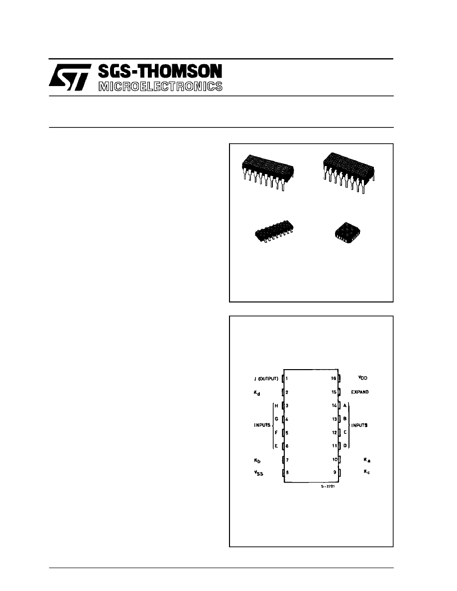
The HCC4048B (extended temperature range) and
HCF4048B (intermediate temperature range) are
monolithic integrated circuit, available in 16-lead
dual in-line plastic or ceramic package and plastic
micro package. The HCC/HCF4048B is an 8-input
gate having four control inputs. Three binary control
inputs - Ka, Kb, and Kc - provide the implementation
of eight different logic functions. These functions are
OR, NOR, AND, NAND, OR/AND, OR/NAND,
AND/OR and AND/NOR. A fourth control input-Kd-
provides the user with a 3-state output. When control
input Kd is high the output is either a logic 1 or a logic
0 depending on the inner states. When control input
Kd is low, the output is an open circuit. This feature
enables the user to connect this device to a common
bus line. In addition to the eight input lines, an EX-
PAND input is provided that permits the user to in-
crease the number of inputs to one HCC/HCF4048B.
For example, two HCC/HCF4048B’s can be cas-
caded to provide a 16-input multifunction gate. When
the EXPAND input is not used, it should be con-
nected to V
SS
.
ORDER CODES :
HCC4048BF
HCF4048BM1
HCF4048BEY
HCF4048BC1
M1
Micro Package
C1
Plastic Chip Carrier
EY
Plastic Package
F
Ceramic Frit Seal Package
PIN CONNECTIONS
1/12
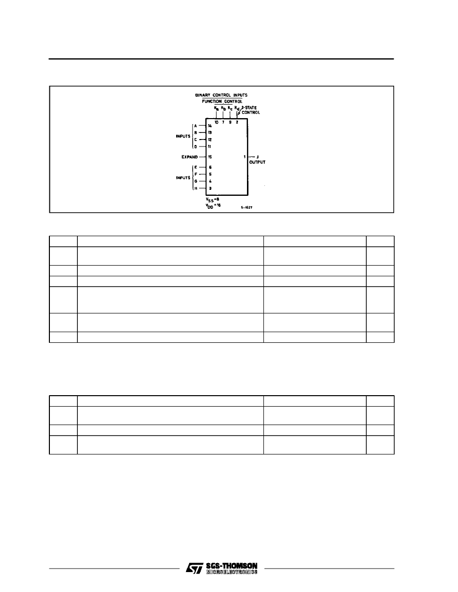
FUNCTIONAL DIAGRAM
ABSOLUTE MAXIMUM RATINGS
Symbol
Parameter
Value
Unit
V
DD
*
Supply Voltage : HC C Types
H C F Types
– 0.5 to + 20
– 0.5 to + 18
V
V
V
i
Input Voltage
– 0.5 to V
DD
+ 0.5
V
I
I
DC Input Current (any one input)
±
10
mA
P
t o t
Total Power Dissipation (per package)
Dissipation per Output Transistor
for T
o p
= Full Package-temperature Range
200
100
mW
mW
T
o p
Operating Temperature : HCC Types
H CF Types
– 55 to + 125
– 40 to + 85
°
C
°
C
T
s t g
Storage Temperature
– 65 to + 150
°
C
RECOMMENDED OPERATING CONDITIONS
Symbol
Parameter
Value
Unit
V
DD
Supply Voltage : HC C Types
H C F Types
3 to 18
3 to 15
V
V
V
I
Input Voltage
0 to V
DD
V
T
o p
Operating Temperature : H CC Types
H C F Types
– 55 to + 125
– 40 to + 85
°
C
°
C
Stresses above those listed under ”Absolute Maximum Ratings” may cause permanent damage to the device. This is a stress rating only
and functional operation of the device at these or any other conditions above those indicated in the operational sections of this specification
is not implied. Exposure to absolute maximum rating conditi ons for external periods may affect device reliability.
* All voltages values are referred to V
SS
pin voltage.
HCC/HCF4048B
2/12
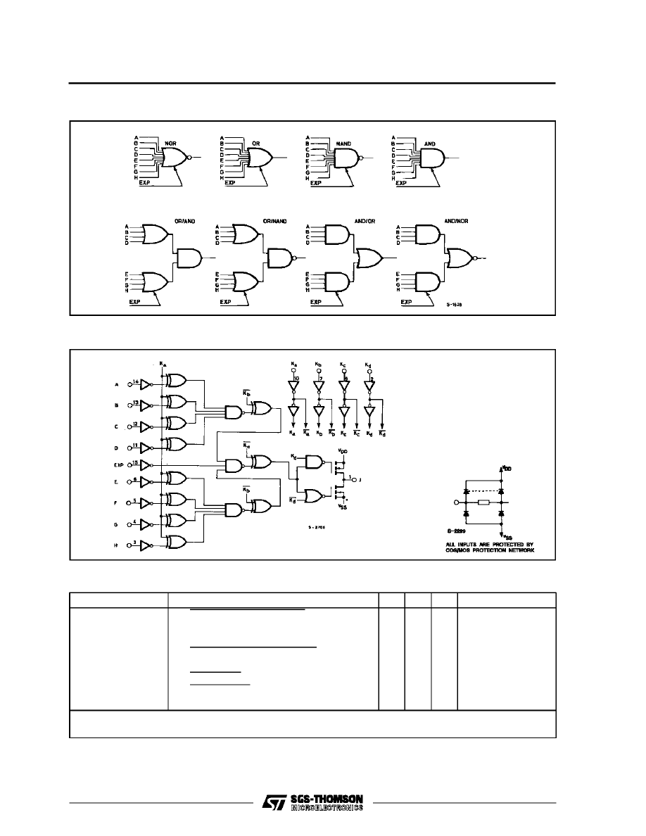
BASIC LOGIC CONFIGURATIONS
LOGIC DIAGRAM
FUNCTION TRUTH TABLE
Output Function
Boolean Expression
K
a
K
b
K
c
Unused Input
NOR
OR
OR/AND
OR/NAND
AND
NAND
AND/NOR
AND/OR
J = A + B + C + D + E + F + G + H
J = A + B + C + D + E + F + G + H
J = (A + B + C + D)
•
(E + F + G + H)
J = (A + B + C + D)
•
(E + F + G + H)
J = ABCDEFGH
J = ABCDEFGH
J = ABCD + EFGH
J = ABCD + EFGH
0
0
0
0
1
1
1
1
0
0
1
1
0
0
1
1
0
1
0
1
0
1
0
1
V
S S
V
S S
V
S S
V
S S
V
DD
V
DD
V
DD
V
DD
K
d
= 1
K
d
= 0
Normal Inverter Action
High Impedance Output
EXPAND Input = 0
HCC/HCF4048B
3/12
STATIC ELECTRICAL CHARACTERISTICS (over recommended operating conditions)
Test Conditions
Value
V
I
V
O
|I
O
|
V
D D
T
L o w
*
25
°
C
T
Hi g h
*
Symbol
Parameter
(V)
(V)
(
µ
A)
(V)
Min. Max. Min. Typ. Max. Min. Max.
Unit
I
L
Quiescent
Current
HCC
Types
0/ 5
5
0.25
0.01
0.25
7.5
µ
A
0/10
10
0.5
0.01
0.5
15
0/15
15
1
0.01
1
30
0/20
20
5
0.02
5
150
HCF
Types
0/ 5
5
1
0.01
1
7.5
0/10
10
2
0.01
2
15
0/15
15
4
0.01
4
30
V
O H
Output High
Voltage
0/ 5
< 1
5
4.95
4.95
4.95
V
0/10
< 1
10
9.95
9.95
9.95
0/15
< 1
15
14.95
14.95
14.95
V
O L
Output Low
Voltage
5/0
< 1
5
0.05
0.05
0.05
V
10/0
< 1
10
0.05
0.05
0.05
15/0
< 1
15
0.05
0.05
0.05
V
IH
Input High
Voltage
0.5/4.5
< 1
5
3.5
3.5
3.5
V
1/9
< 1
10
7
7
7
1.5/13.5
< 1
15
11
11
11
V
IL
Input Low
Voltage
4.5/0.5
< 1
5
1.5
1.5
1.5
V
9/1
< 1
10
3
3
3
13.5/1.5
< 1
15
4
4
4
I
O H
Output
Drive
Current
HCC
Types
0/ 5
2.5
5
– 2
– 1.6 – 3.2
– 1.15
mA
0/ 5
4.6
5
– 0.64
– 0.51 – 1
– 0.36
0/10
9.5
10
– 1.6
– 1.3 – 2.6
– 0.9
0/15
13.5
15
– 4.2
– 3.4 – 6.8
– 2.4
HCF
Types
0/ 5
2.5
5
– 1.53
– 1.36 – 3.2
– 1.1
0/ 5
4.6
5
– 0.52
– 0.44 – 1
– 0.36
0/10
9.5
10
– 1.3
– 1.1 – 2.6
– 0.9
0/15
13.5
15
– 3.6
– 3.0 – 6.8
– 2.4
I
O L
Output
Sink
Current
HCC
Types
0/ 5
0.4
5
0.64
0.51
1
0.36
mA
0/10
0.5
10
1.6
1.3
2.6
0.9
0/15
1.5
15
4.2
3.4
6.8
2.4
HCF
Types
0/ 5
0.4
5
0.52
0.44
1
0.36
0/10
0.5
10
1.3
1.1
2.6
0.9
0/15
1.5
15
3.6
3.0
6.8
2.4
I
IH
, I
IL
Input
Leakage
Current
HCC
Types
0/18
Any Input
18
±
0.1
±
10
-5
±
0.01
±
1
µ
A
HCF
Types
0/15
15
±
0.3
±
10
-5
±
0.3
±
1
I
O H
3-state
Output
Current
HCC
Types
0/18
0/18
18
±
0.4
±
10
-4
±
0.4
±
12
µ
A
HCF
Types
0/15
0/15
15
±
1.0
±
10
-4
±
1.0
±
7.5
C
I
Input Capacitance
Any Input
5
7.5
pF
* T
LOW
= – 55
°
C for HCC device : – 40
°
C for HCF device.
* T
HIG H
= – 125
°
C for HCC device : – 85
°
C for HCF device.
The Noise Margin for both ”1” and ” 0” level is : 1V min. with V
DD
= 5V, 2V min. with V
DD
= 10V, 2.5V min. with V
DD
= 15V,
HCC/HCF4048B
4/12
DYNAMIC ELECTRICAL CHARACTERISTICS (T
amb
= 25
°
C, C
L
= 50pF, R
L
= 200k
Ω
,
typical temperature coefficient for all V
DD
= 0.3%/
°
C values, all input rise and fall time = 20ns)
Test Conditions
Val ue
Symbol
Parameter
V
D D
(V)
Min.
Typ.
Max.
Unit
t
PHL
, t
PL H
Propagation Delay Time Inputs
to Output and Ka to Output
5
300
600
ns
10
150
300
15
120
240
Kb to Output
5
225
450
10
85
170
15
55
110
Kc to Output
5
140
280
10
50
100
15
40
80
Expand Input to Output
5
190
380
10
90
180
15
65
130
t
PHZ
, t
PL Z
t
PZ H
, t
PZ L
3–state Propagation Delay Time
Kd to Output
R
L
= 1k
Ω
5
80
160
10
35
70
15
25
50
t
T HL
, t
TL H
Transition Time
5
100
200
10
50
100
15
40
80
3-state Output Capacitance
5
10
pF
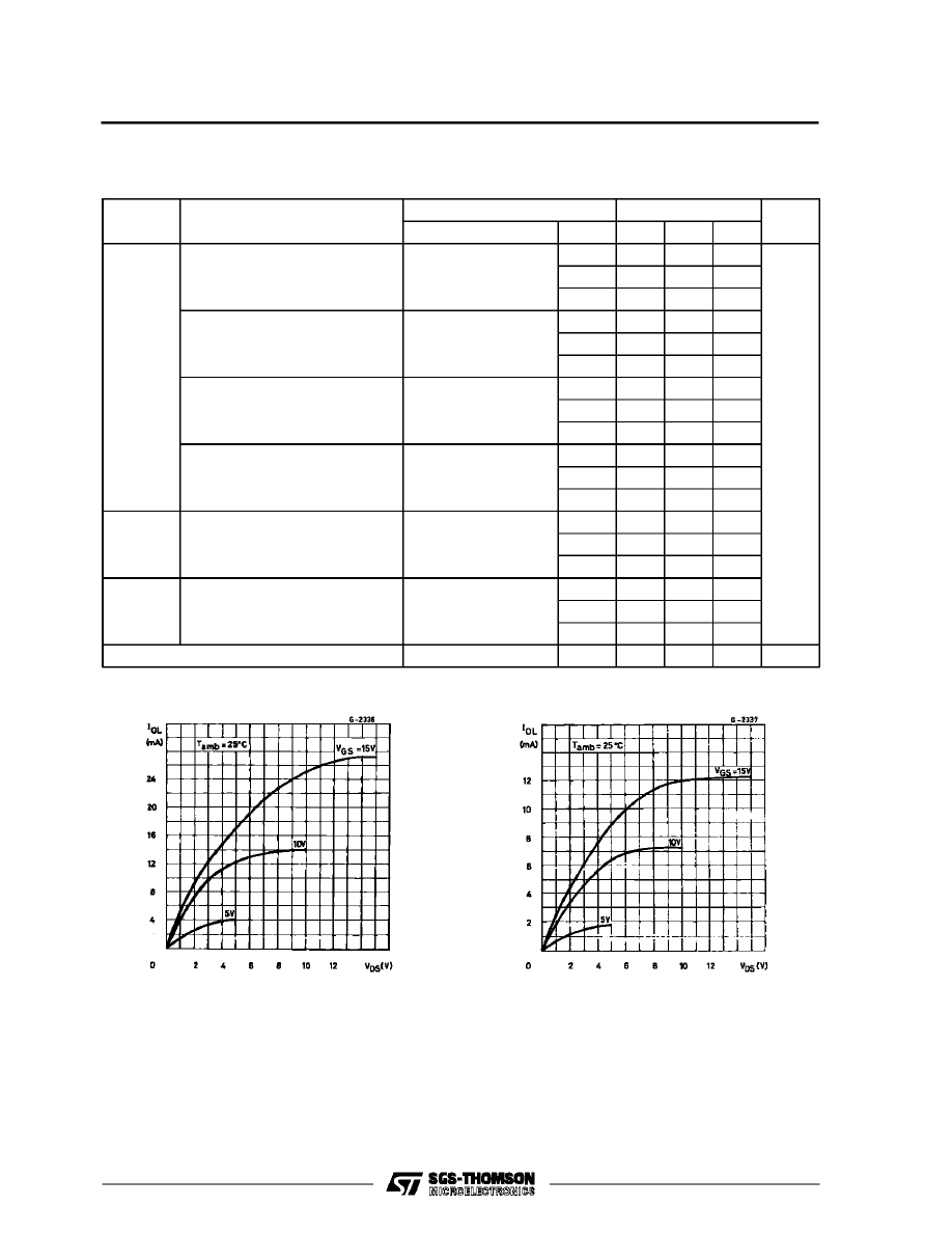
Typical Output Low (sink) Current Characteristics.
Minimum Output Low (sink) Current Characteristics.
HCC/HCF4048B
5/12
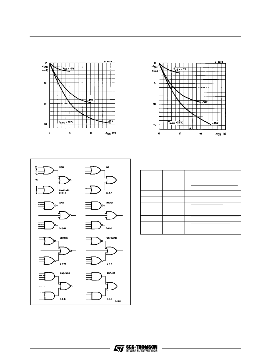
Typical Output High (source) Current Charac-
teristics.
Minimum Output high (source) Current Charac-
teristics.
APPLICATIONS OF EXPAND INPUT
ACTUAL-CIRCUIT LOGIC CONFIGURATIONS
EXPANSION LOGIC AND TRUTH TABLE
Note : (EXP) designates the EXPAND function (i.e., X
1
+ X
2
+ . . X
N
).
IMPLEMENTATION OF EXPAND INPUT
FOR 9 OR MORE INPUTS
OUTPUT
FUNCTION
FUNCTION
NEEDEDAT
EXPANDINPUT
OUTPUT BOOLEAN EXPRESSION
NOR
OR
J = (A+B+C+D+E+F+G+H) + (EXP)
OR
OR
J = (A+B+C+D+E+F+G+H) + (EXP)
AND
NAND
J = (ABCDEFGH)
⋅
(EXP)
NAND
NAND
J = (ABCDEFGH)
⋅
(EXP)
OR/AND
NOR
J = (A+B+C+D)
⋅
(E+F+G+H)
⋅
(EXP)
OR/NAND
NOR
J = (A+B+C+D)
⋅
(E+F+G+H)
⋅
(EXP)
AND/NOR
AND
J = (ABCD) + (EFGH) + (EXP)
AND/OR
AND
J = (ABCD) + (EFGH) + (EXP)
HCC/HCF4048B
6/12
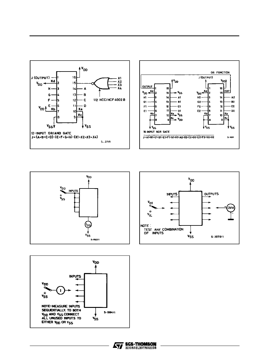
12-Input or/and Gate.
16-Input Nor Gate.
APPLICATIONS OF EXPAND INPUT (continued)
TEST CIRCUITS
Input Voltage.
Quiescent Device Current.
Input Current.
HCC/HCF4048B
7/12
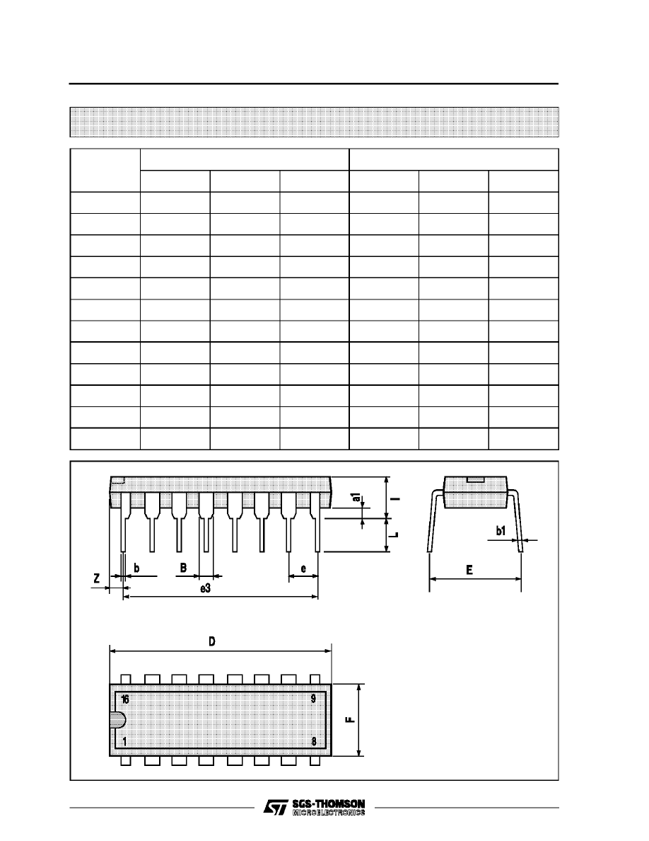
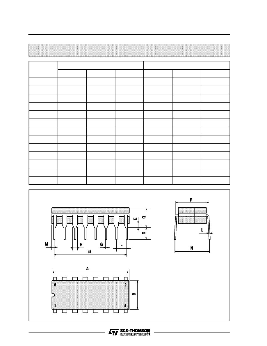
Plastic DIP16 (0.25) MECHANICAL DATA
DIM.
mm
inch
MIN.
TYP.
MAX.
MIN.
TYP.
MAX.
a1
0.51
0.020
B
0.77
1.65
0.030
0.065
b
0.5
0.020
b1
0.25
0.010
D
20
0.787
E
8.5
0.335
e
2.54
0.100
e3
17.78
0.700
F
7.1
0.280
I
5.1
0.201
L
3.3
0.130
Z
1.27
0.050
P001C
HCC/HCF4048B
8/12
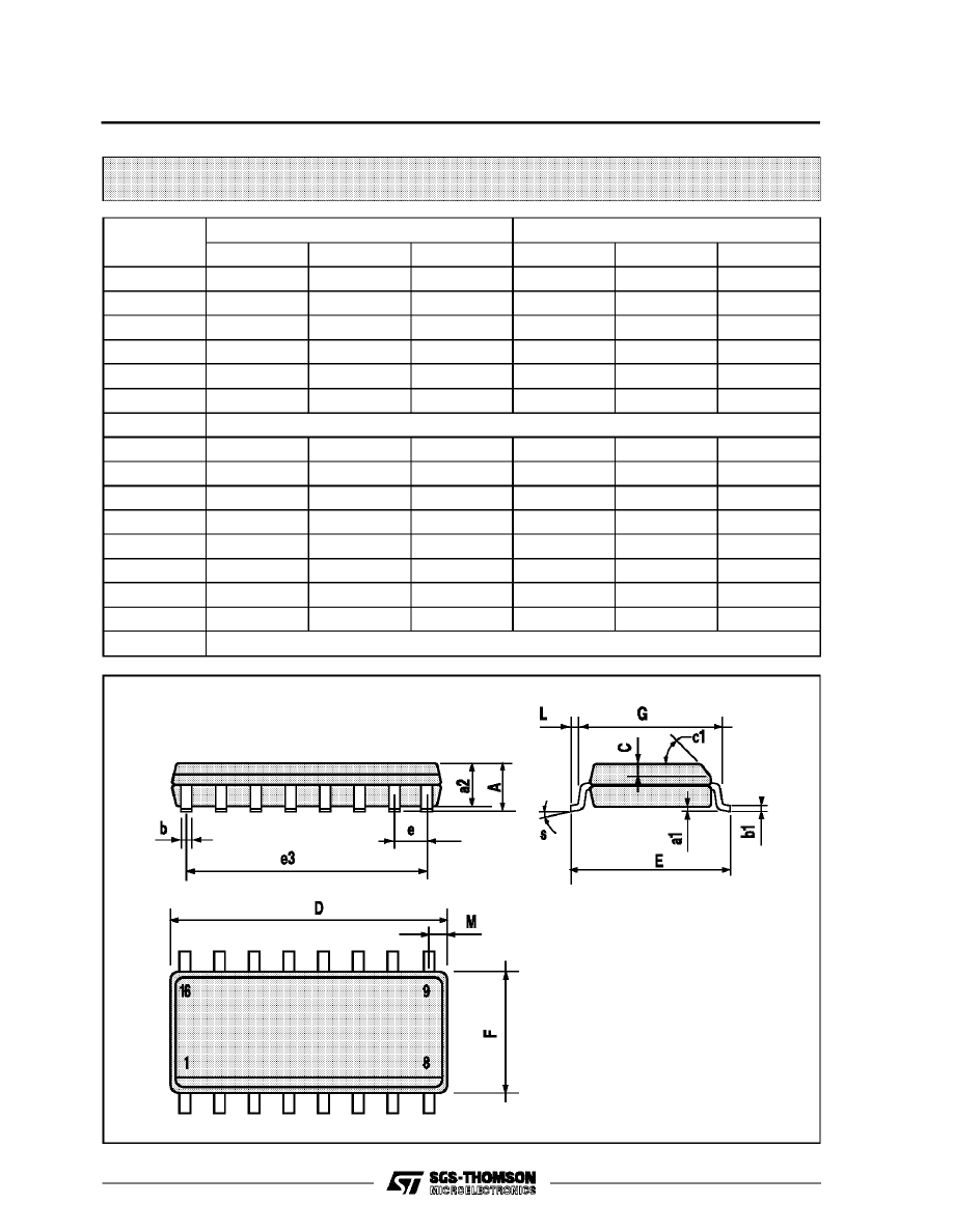
Ceramic DIP16/1 MECHANICAL DATA
DIM.
mm
inch
MIN.
TYP.
MAX.
MIN.
TYP.
MAX.
A
20
0.787
B
7
0.276
D
3.3
0.130
E
0.38
0.015
e3
17.78
0.700
F
2.29
2.79
0.090
0.110
G
0.4
0.55
0.016
0.022
H
1.17
1.52
0.046
0.060
L
0.22
0.31
0.009
0.012
M
0.51
1.27
0.020
0.050
N
10.3
0.406
P
7.8
8.05
0.307
0.317
Q
5.08
0.200
P053D
HCC/HCF4048B
9/12
SO16 (Narrow) MECHANICAL DATA
DIM.
mm
inch
MIN.
TYP.
MAX.
MIN.
TYP.
MAX.
A
1.75
0.068
a1
0.1
0.2
0.004
0.007
a2
1.65
0.064
b
0.35
0.46
0.013
0.018
b1
0.19
0.25
0.007
0.010
C
0.5
0.019
c1
45
°
(typ.)
D
9.8
10
0.385
0.393
E
5.8
6.2
0.228
0.244
e
1.27
0.050
e3
8.89
0.350
F
3.8
4.0
0.149
0.157
G
4.6
5.3
0.181
0.208
L
0.5
1.27
0.019
0.050
M
0.62
0.024
S
8
°
(max.)
P013H
HCC/HCF4048B
10/12
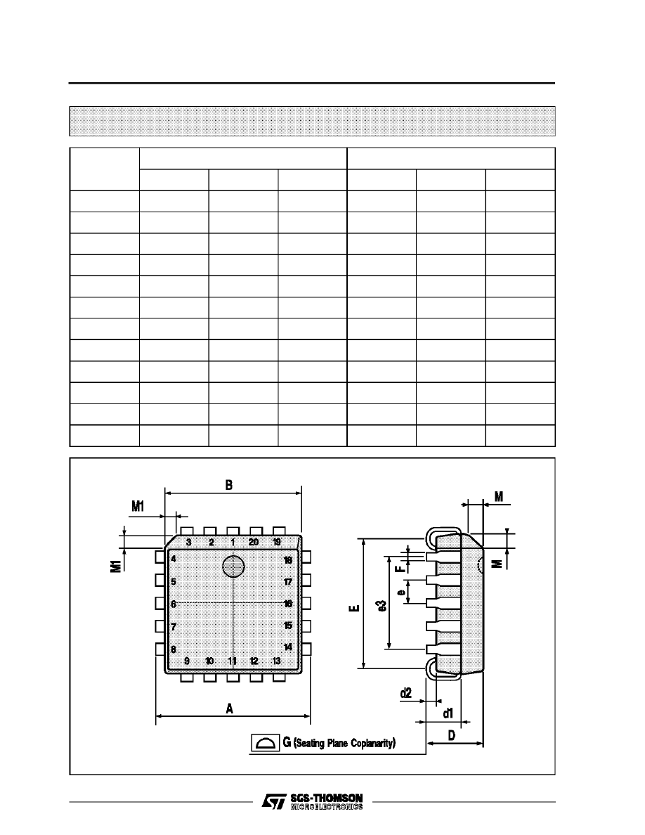
PLCC20 MECHANICAL DATA
DIM.
mm
inch
MIN.
TYP.
MAX.
MIN.
TYP.
MAX.
A
9.78
10.03
0.385
0.395
B
8.89
9.04
0.350
0.356
D
4.2
4.57
0.165
0.180
d1
2.54
0.100
d2
0.56
0.022
E
7.37
8.38
0.290
0.330
e
1.27
0.050
e3
5.08
0.200
F
0.38
0.015
G
0.101
0.004
M
1.27
0.050
M1
1.14
0.045
P027A
HCC/HCF4048B
11/12

Information furnished is believed to be accurate and reliable. However, SGS-THOMSON Microelectronics assumes no responsability for the
consequences of use of such information nor for any infringement of patents or other rights of third parties which may results from its use. No
license is granted by implication or otherwise under any patent or patent rights of SGS-THOMSON Microelectronics. Specifications mentioned
in this publication are subject to change without notice. This publication supersedes and replaces all information previously supplied.
SGS-THOMSON Microelectronics products are not authorized for use as critical components in life support devices or systems without express
written approval of SGS-THOMSON Microelectonics.
1994 SGS-THOMSON Microelectronics - All Rights Reserved
SGS-THOMSON Microelectronics GROUP OF COMPANIES
Australia - Brazil - France - Germany - Hong Kong - Italy - Japan - Korea - Malaysia - Malta - Morocco - The Netherlands -
Singapore - Spain - Sweden - Switzerland - Taiwan - Thailand - United Kingdom - U.S.A
HCC/HCF4048B
12/12
Wyszukiwarka
Podobne podstrony:
PCG2 Package OFR 90 4048
4048
4048
przekroj podluzny plyty id 4048 Nieznany
4048
PRZEKROJ ZE SZCZEGOLAMI id 4048 Nieznany
4048
4048
02Eid 4048
4048
4048
przekladnie mechaniczne id 4048 Nieznany
PCG2 Package OFR 90 4048
PCG2 Package OFR 90 4048
4048 ac
więcej podobnych podstron