www.powerint.com
Design Idea DI-30
TOPSwitch-GX
180 W PC Main SFX Supply
December 2002
DI-30
®
Application
PC Main
TOP249Y
3.3 V / 5 V / 12 V / -12 V
Power Output
180 W
Input Voltage
Output Voltage
Topology
Device
90-130 VAC / 180-265 VAC
Forward
Design Highlights
• 180 W cont. (200 W peak) in PC SFX form factor
• Includes passive power factor correction (PFC)
• TOPSwitch-GX integrated features enable extremely low
component count
• Meets 1 W standby spec (0.91 W input, 0.5 W output)
• High efficiency (71% minimum)
• Integrated line undervoltage and overvoltage detection
• Low EMI due to frequency jitter
• SOURCE referenced TO-220 tab lowers conducted EMI
• Maximum duty cycle reduction (DC
MAX
) prevents transformer
saturation for fault and transient loads
• Uses conventional magamp for 3.3 V output
• Meets CISPR22B/EN55022B conducted EMI
Operation
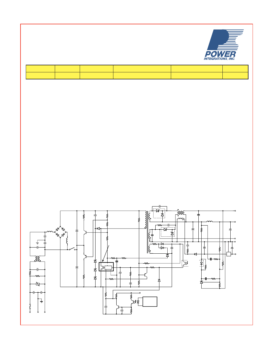
TOPSwitch-GX integrates many features designed for use with
forward converters. Passive power factor correction (PFC) is
implemented using inductors LPFC1 and LPFC2. Transistors
Q4, Q6, R1, R2, R3, R5, and R6 form an active capacitor (C2,
Figure 1.
180 W (200 W pk.) PC Main Power Supply Schematic (Note: Schematic does not include transformer Y-capacitor)
.
C3) balancing circuit, operating only as needed to minimize
zero-load power consumption.
Resistors R3, R5 and R6 implement start-up undervoltage
lockout, which prevents the supply from starting below
180 VDC. Components R4, R14, Q1 and R30 implement an
independent undervoltage using the X pin, which allows the
supply to continue delivering power all the way down to
140 VDC (increasing holdup time). Resistor R7 provides
additional hysteresis.
The primary side components D1, VR3-5 and C4, along with
secondary side C9 and R30, implement the Zener/capacitor
reset/clamp circuit. This circuit provides reset voltage for the
transformer and clamps the DRAIN pin voltage to a safe level
(<~600 V) under all conditions.
The reset circuit works in conjunction with the DC
MAX
reduction circuit (R8, R36, C22, VR19 and D18) to limit the
maximum duty cycle and prevent transformer saturation
under fault and transient conditions.
®
C13
220 µF
63 V
C3
470 µF
200 V
C2
470 µF
200 V
L
G
N
RTN
+5 V
+12 V
R20
270 kΩ
R16
1 kΩ
U5
TL431
D
S
C
L
F
X
CONTROL
R19
4.12 kΩ
1%
F1
4 A
RV1
275 V, 14 mm
R10
560 K
1/2 W
CX2
0.33 µF
250V
CY4
2.2 nF
(Safety)
RT1
10 Ω
CY3
2.2 nF
(Safety)
JP9
CX1
0.047 µF
250 VAC
L7
8.2 mH
BR1
KBL06
To AC Selector
Switch
R1
330 kΩ
R2
330 kΩ
D1
1N5407
R3
2.2 MΩ
R5
180 kΩ
R6
2.2 MΩ
R8
130 kΩ
1%
R14
75 kΩ
R12
12 kΩ
R30
3.3 kΩ
Q1
2N3908
C22
100 pF
50 V
C10
1 nF
50 V
C20
330 pF
50 V
D7
MBR3045
R36
43.2 kΩ
1%
R13
10 Ω
D18
BAV20
VR19
1N5229
R4
2.2 MΩ
R7
560 kΩ
R11
300 Ω
Coupled
choke
L1
13 µH
R30
1 Ω
1 W
D8
MBR6045
C9
47 nF
50 V
C12
2200 µF
6.3 V
C11
1000 µF
16 V
L2
0.5 µH
U2
SFH615A-2
R17
15 kΩ
C16
100 nF
50 V
D6
BAV20
C8
0.033
µ
F
50 V
R9
47 Ω
C6
47
µ
F
16 V
C7
100 nF
50 V
D105
1N4148
Remote
ON/OFF
R38
5.1 kΩ
U3
LTV817
R37
10 kΩ
R106
27 kΩ
+12 V STBY
C23
33 nF
50 V
VR3
BZY97C-
200
C4
2.2 nF
1 kV
VR4
BZY97C-
180
VR5
BZY97C-
180
D20
UF4002
C5
1
µ
F
100 V
C27
330 pF
50 V
R11
330 Ω
LM
320
C25
1 µF
50 V
TO
MAGAMP OUT
(3.3 V)
- 12 V
R18
4.74 kΩ
1%
R15
1.8 kΩ
C17
100 nF
50 V
C24
330 µF
25 V
Q7
2N3904
PI-3384-120902
TOPSwitch-GX
U1
TOP249
2
1
13
14
11,12
8, 9, 10
4
3
4
5
1, 2
7, 8
3
6
Q6
MPSA92
Q4
MPSA42
R21
270 Ω
LPFC1
LPFC2

www.powerint.com
B
12/02
DI-30
WORLD HEADQUARTERS
AMERICAS
Power Integrations, Inc.
San Jose, CA 95138 USA
Customer Service:
Phone:
+1 408-414-9665
Fax:
+1 408-414-9765
e-mail: usasales@powerint.com
CHINA
Power Integrations International
Holdings, Inc.
China
Phone:
+86-755-8367-5143
Fax:
+86-755-8377-9610
e-mail: chinasales@powerint.com
SINGAPORE
Power Integrations, Singapore
Republic of Singapore 308900
Phone:
+65-6358-2160
Fax:
+65-6358-2015
e-mail: singaporesales@powerint.com
JAPAN
Power Integrations, K.K.
Keihin-Tatemono 1st Bldg.
Japan
Phone:
+81-45-471-1021
Fax:
+81-45-471-3717
e-mail: japansales@powerint.com
EUROPE & AFRICA
Power Integrations (Europe) Ltd.
United Kingdom
Phone:
+44-1344-462-300
Fax:
+44-1344-311-732
e-mail: eurosales@powerint.com
KOREA
Power Integrations
International Holdings, Inc.
Seoul, Korea
Phone:
+82-2-782-2840
Fax:
+82-2-782-4427
e-mail: koreasales@powerint.com
TAIWAN
Power Integrations
International Holdings, Inc.
Taipei, Taiwan
Phone:
+886-2-2727-1221
Fax:
+886-2-2727-1223
e-mail: taiwansales@powerint.com
INDIA (Technical Support)
Innovatech
Bangalore, India
Phone:
+91-80-226-6023
Fax:
+91-80-228-9727
e-mail: indiasales@powerint.com
APPLICATIONS HOTLINE APPLICATIONS FAX
World Wide +1-408-414-9660 World Wide +1-408-414-9760
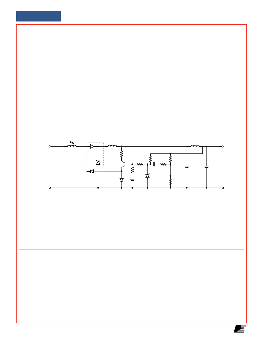
Figure 2. Magamp for Independent 3.3 V Secondary Regulation.
The components R12, C7, R38, Q7, C23, R37, U3, R106 and
D105 implement the remote ON/OFF drive circuit. During
the ON state, U3 and hence Q7 conduct, pulling the X pin to
SOURCE via resistor R12 (which sets the current limit).
During the OFF state, U3 and Q7 are off, allowing the X pin
to be pulled high by the +15 V standby supply via R38 and R12
and putting the TOPSwitch-GX into the OFF state. Components
R38 and D105 reduce device consumption to around 2mW by
supplying external current to the CONTROL pin from the
+15 V standby supply. Resistor R11 is required to allow
external bias feed.
Key Design Points
• The passive PFC inductors (LPFC1 and LPFC2) are
constrained by both thermal and efficiency requirements.
Design of these inductors is not covered in this Design Idea.
• Transformer reset: Use recommended Zener/capacitor
clamp/reset circuit to maintain drain voltage < 600 V and
DC
MAX
reduction to prevent transformer saturation.
• Maintain maximum flux density on transformer (T1)
< 2500 gauss.
• Check for balanced currents on coupled inductor (L1) for
all load combinations.
• Use PI Expert (PIXls) Design Spreadsheet and refer to
Application Note AN-30 for details on designing forward
converters with TOPSwitch-GX.
This particular PC SFX 12 specification delivers a larger
proportion of power on the 12 V winding; efficiency would be
lower if that power were drawn from the 3.3 V output.
Due to the complexity of this design it is not possible to include
all details in this Design Idea. An Engineering Prototype Report
(EPR) will be available for this design Dec. 2000. For updates
and all other information please refer to Power Integrations'
Web site.
For the latest updates, visit our Web site: www.powerint.com
Power Integrations reserves the right to make changes to its products at any time to improve reliability or manufacturability.
Power Integrations does not assume any liability arising from the use of any device or circuit described herein, nor does it convey any
license under its patent rights or the rights of others. The products and applications illustrated herein (including circuits external to the
products and transformer construction) may be covered by one or more U.S. and foreign patents or potentially by pending U.S. and foreign
patent applications assigned to Power Integrations. A complete list of Power Integrations’ patents may be found at www.powerint.com.
The PI Logo, TOPSwitch, TinySwitch, LinkSwitch and EcoSmart are registered trademarks of Power Integrations, Inc.
PI Expert is a trademark of Power Integrations, Inc. ©Copyright 2002, Power Integrations, Inc.
3.3 V
RTN
RTN
PI-3385-093002
D11
UF4002
D10
UF4002
R22
3 Ω
Q2
TIP32
D9
MBR2045
L4
20 µH
L5
0.5 µH
R34
33 Ω
R27
390 Ω
R23
1 kΩ
R25
2.7 kΩ
C18
0.1 µF
50 V
R24
3.84 kΩ
1%
R26
10 kΩ
1%
U8
TL431
C21
1 µF
50 V
L3
Mag Amp
6 Turns
C14
1200 µF
10 V
C15
1200 µF
10 V
FROM MAIN
CONVERTER
5 V WINDING
Wyszukiwarka
Podobne podstrony:
PS i PC ćwiczenia
PS i PC- teoria, Present Simple i Present Continuous
PS-PC podsumowanie, Present Simple i Present Continuous
kartkówka PS vs PC
test used to, PS, PC, PP, PPC
ps pc 2
C czasowniki ze zmianą znaczenia PS i PC PL
ps i pc ćw
ps pc
C czasowniki ze zmianą znaczenia PS i PC ANG
ps pc (2)
PS VI
PS spolecznosc lokalna 3
PS 1 Psychologia społeczna wstep
BUDOWA KOMPUTERA PC
PS Organiz 11
więcej podobnych podstron