H
igh-side drivers find common
use in driving grounded so-
lenoid coils and other loads.
Short-circuit protection for such drivers
is essential for avoiding damage from
wiring faults and other causes. Polymer
fuses are generally too slow, and discrete
current-limiting circuits are large and
cumbersome. The circuit in Figure 1 uses
a small, low-dropout linear regulator as a
high-side switch and provides inherent
current limiting and thermal shutdown.
The regulator comes in an SO-8 package.
The zener diode provides transient pro-
tection, and the output capacitor ensures
stability of the circuit. The circuit can
drive a 24V load at 100 mA. These
are adequate specs for many sole-
noid valves, relay coils, and other moder-
ate loads. During a short circuit, the reg-
ulator limits the current to 160 mA. This
current causes the die to overheat and en-
ter a thermal-shutdown state. Upon re-
moval of the short circuit, the device
cools down and resumes normal opera-
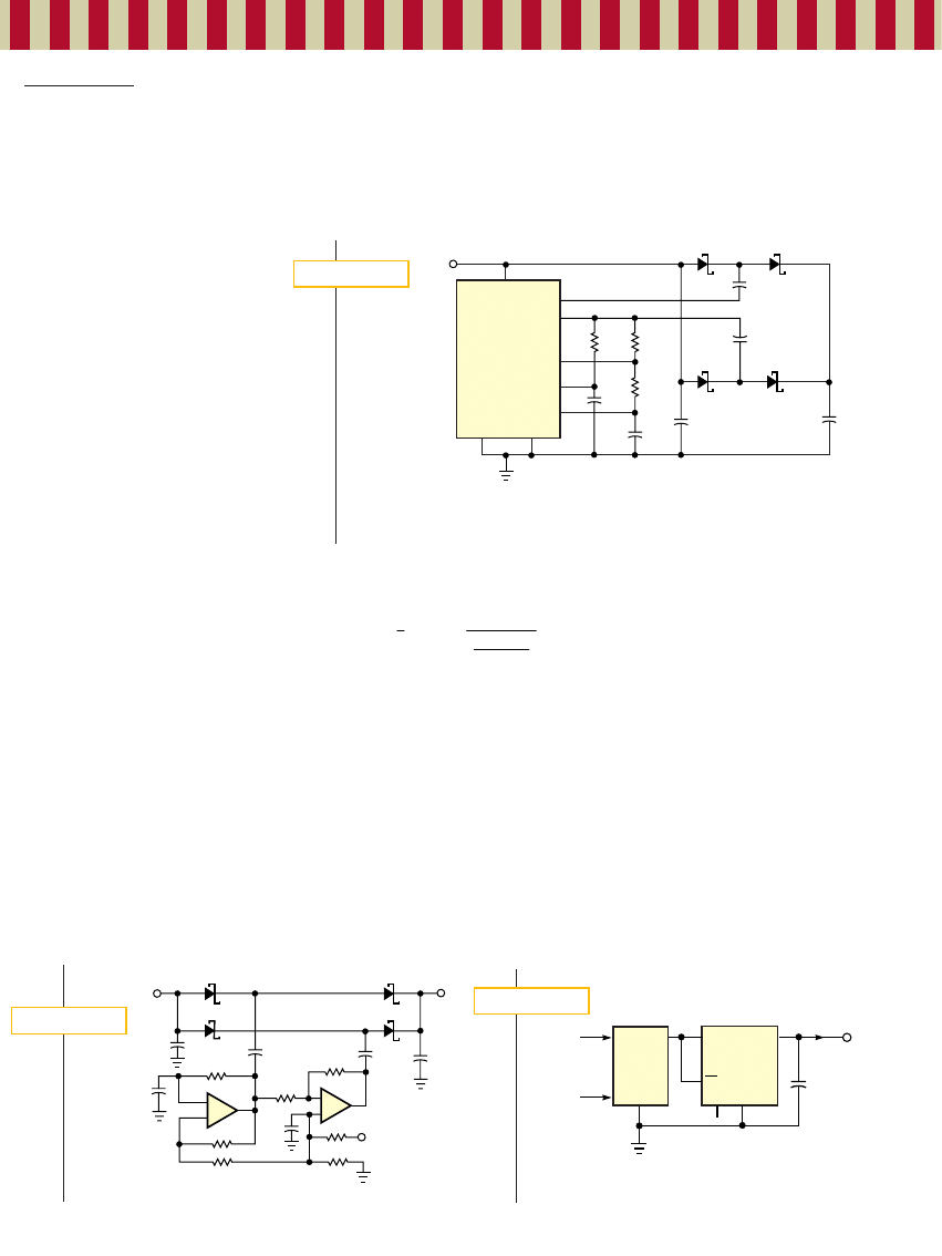
tion. The top trace in Figure 2 is the out-
put voltage during a 1.3-sec short circuit.
The bottom trace is the short-circuit cur-
rent, which limits itself at less than 200
mA. Note that the regulator goes into
thermal shutdown after 500 msec, and
the IC then toggles on and off until re-
moval of the short circuit.
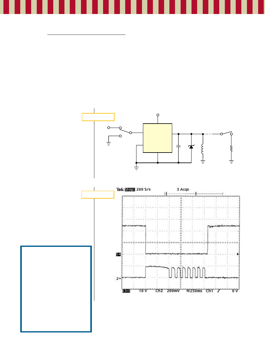
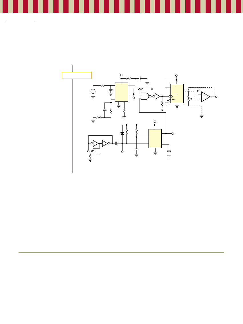
IN
OUT
SHDN
FB
GND
24V
IC
1
LP2951 (SO-8)
ON
OFF
5V
LOAD
1
SHORT-CIRCUIT TEST
30V
1
F
4
3
7
8
1
edn020822di298011
Heather
F i g u r e 1
High-side driver has fault protection
Carl Spearow, Tokyo Electron, Gilbert, AZ
This simple high-side driver provides current limiting as well as transient protection.
F i g u r e 2
In the bottom trace, the output current limits itself to 160 mA during a short circuit.
Is this the best Design Idea in this
issue? Select at www.edn.com.
www.edn.com
September 5, 2002 | edn
103
ideas
design
High-side driver has fault protection ......
103
Boost 3.3V to 5V with tiny
audio amplifier ............................................
104
Add a signal-strength display
to an FM-receiver IC....................................
106
Op amp linearizes response
of FET VCA ....................................................
108
Convert voltage to potentiometer-
wiper setting ..................................................
110
Make a DAC with a micro-
controller’s PWM timer ..............................
110
Publish your Design Idea in EDN. See the
What’s Up section at www.edn.com.
Edited by Bill Travis
104
edn | September 5, 2002
www.edn.com
ideas
design
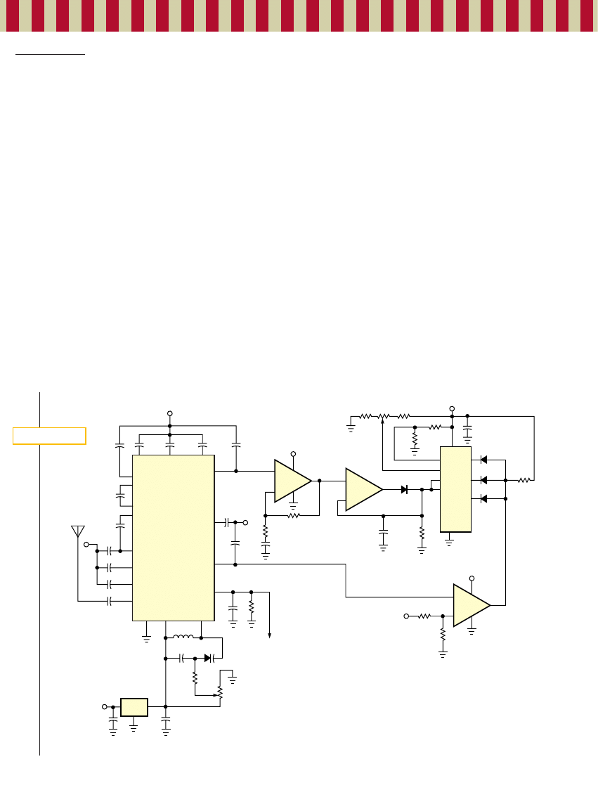
T
his charge-pump circuit quietly
converts a 3.3V source to 5V
at 500 mA (figures 1 and 2).
National’s (www.national.com) LM48-
71LD power amplifier makes this design
idea both possible and practical, thanks
to its low output resistance, low cost,
compact size, and high dissipation capa-
bility. Its output resistance has an average
value of 0.6
⍀: 0.5⍀ to ground and 0.7⍀
to V
IN
. Because it is a CMOS IC, each out-
put can swing to its rail, limited only by
the resistance of the output transistor.
The leadless lead-frame package has a
footprint smaller than an SO-8 but pro-
vides a
JA
of 56
⬚C/W when soldered to a
board with 1 sq in. of 1-oz copper ex-
posed. This high thermal conductivity
couples with low output resistance to al-
low the 4871 to continuously deliver
nearly 1A from each of its two outputs
while operating at its full rated ambient
temperature of 85
⬚C. Internal thermal
shutdown protects the device from over-
loads, and a shutdown pin allows you to
power down the device to less than 1
A.
Figure 2 shows the full circuit
schematic, including the equivalent in-
ternal components. Amplifier IC
1
is con-
figured as an RC oscillator similar to a
555 timer. R
T
charges C
T
to the voltage set
by the resistor divider R
H1
and R
H2
, caus-
ing the amplifier to switch states, aided by
the positive feedback from the R
H
resis-
tors. The remaining internal feedback
and biasing resistors connected to IC
2
configure it as a simple inverter with bias
at mid-supply. The amplifier outputs
switch rail-to-rail out of phase with a
50% duty cycle at a frequency approxi-
mated by the following equation:
You can calculate the output voltage
across C
OUT
from the following equation:
where I
OUT
is the average output current,
V
DIODE
is the diode voltage drop at I
OUT
,
R
S
is the source resistance of IC
1
and IC
2
,
ESR is that of C
1
and C
2
, and C is the val-
ue of C
1
⫽C
2
.
The following equation approximates
the effective output resistance at the load:
Component values as shown in Figure
1 provide a circuit that can produce 5V at
0.5A from a 3.3V source at a conversion
efficiency of 78%. If necessary, you can
obtain tighter regulation figures at slight-
ly lower output current by adding a low-
dropout linear regulator, such as the
LP3961. At a 500-mA load it introduces
a drop of only 150 mV. Its addition pro-
vides good line and load regulation over
the range I
OUT
⫽0 to 500 mA (Figure 3).
You can also use the circuits of figures 1
and 3 to provide 3.3V at 500 mA from a
2.5V source.
V
IN
A2OUT
A1OUT
LM4871LD
R
S
0.6
⍀
SD
GND
BP
A1+
A1
ⳮ
1
7
V
IN
3.3V
6
8
5
NOTES:
1. D
1
AND D
2
: MBRS12OT3.
2. C
1
AND C
2
ESR<11
⍀.
C
1
150
F
16V
C
2
150
F
16V
C
OUT
150
F
16V
C
IN
150
F
16V
C
BP
1
F
C
T
4.7 nF
3
4
2
R
T
10k
R
H1
300k
R
H2
33k
D
2
D
4
D
1
D
3
+
+
+
F i g u r e 1
Boost 3.3V to 5V with tiny audio amplifier
Wayne Rewinkel, National Semiconductor, Santa Clara, CA
You can use a tiny audio amplifier to boost 3.3V to 5V with respectable current capability.
+
40k
40k
IC
2
IC
1
A2
OUT
A1
OUT
C
OUT
V
IN
D
1
D
2
C
IN
C
1
V
OUT
D
3
D
4
C
2
BP
C
BP
100k
100k
V
IN
R
H1
R
H2
C
T
R
T
A1+
A1
ⳮ
3.3V
This equivalent circuit shows the innards of the LM4871LD audio amplifier.
DOUBLER
CIRCUIT
3.3V
VIN
VOUT
LP3961EMPX
V
OUT
5V, 5A
SD
2
3
1
ERR GND
4
5
C
OUT
⬎10 F
SD
F i g u r e 3
F i g u r e 2
You can tighten voltage-regulation specs in Figure 1’s circuit by
adding a linear regulator.
Is this the best Design Idea in this
issue? Select at www.edn.com.
.
kHz
53
TO
44
f
,
R
R
R
C
R
4
SEC
4
f
1
2
H
2
H
1
H
T
T
=
+
+
µ
=
(
)
,
V
08
.
5
)
062
.
0
05
.
0
3
.
0
35
.
0
3
.
3
(
2
Cf
/
I
)
ESR
(
I
R
I
V
V
2
V
OUT
OUT
S
OUT
DIODE
IN
OUT
=
=
=
ⳮ
ⳮ
ⳮ
ⳮ
ⳮ
ⳮ
ⳮ
ⳮ
(
)
.
9
.
1
)
07
.
0
11
.
0
15
.
0
6
.
0
(
2
Cf
/
1
ESR
R
R
2
R
DIODE
S
OUT
⍀
=
+
+
+
=
+
+
+
=
106
edn | September 5, 2002
www.edn.com
ideas
design
T
he Philips (www.semiconductors.
philips.com) TDA7000 integrates a
monaural FM-radio receiver from
the antenna connection to the audio out-
put. External components include one
tunable LC circuit for the local oscillator,
a few capacitors, two resistors, and a po-
tentiometer to control the variable-ca-
pacitance-diode tuning. The IC has an
FLL (frequency-locked-loop) structure.
The filtered output of the FM discrimi-
nator frequency-modulates the local os-
cillator to provide negative-feedback
modulation. The result is compression of
the signal at the output of the mixer.
Thus, the IF bandpass filter and the FM
discriminator deal with narrowband FM
signals. For a compression factor of K
⫽3,
the original FM bandwidth reduces to
180/3
⫽60 kHz. So, you need neither ce-
ramic filters nor complex LC tank cir-
cuits to realize the IF filter. A simple ac-
tive filter using op amps can fulfill the
task. The IC incorporates a correlation
muting system that suppresses intersta-
tion noise and spurious responses aris-
ing from detuning. The muting circuit
uses a second mixer. Its output is avail-
able at Pin 1; you can use it to drive a de-
tuning indicator. You can add a signal-
strength display to the TDA7000 using
the circuit in Figure 1.
You can obtain the information relat-
ed to the intensity of the received signal
at the output of the IF filter (IC
1
, Pin 12).
You can easily process this voltage with
common op amps, because the IF signal
is centered on 70 kHz. The voltage at Pin
12 is dc-coupled to an amplifier, IC
2
.
Next, an envelope detector, IC
3
, yields a
dc voltage proportional to the received-
signal strength. The Siemens (www.
siemens.com) TCA965 window discrim-
inator, IC
4
, compares this envelope volt-
age with a voltage derived from R
1
, R
2
,
and R
3
for the window’s center (and R
4
and R
5
for the window’s half-width).
Three LEDs show the result of the com-
parison (Low, OK, Good), but the display
is valid only if the tuning is correct. If it’s
correct, the voltage at IC
1
, Pin 1 reaches
its maximum value, and the LM311
comparator, IC
5
, enables the TCA965.
IC
1
TDA7000
8
7
9
10
11
14
17
13
3.3 nF
2.2 nF
330 pF
330 pF
180 pF
39 pF
5V
3.3 nF
10 nF
220 pF
150 pF
100 nF
5
16
6
15
4
18
L
1
56 nH
5V
12
1/2
TL082
1/2
TL082
IC
5
LM311
_
+
9V
IC
2
IC
3
3
1
2
22 nF
150
nF
1.8
nF
4.7 nF
1k
TO AUDIO
AMPLIFIER
20k
10 nF
10 nF
BB809
100k
10k
5V
IC
6
7805
9V
10
F
22k
5V
1N4148
7
1
6
13
14
8
9
2
IC
4
TCA965
11
_
+
_
+
9V
R
5
4.7k
R
4
220k
R
1
20k
R
2
5k
R
3
20k
10 nF
1k
GOOD
OK
LOW
9V
12k
10k
9V
100k
2.2
F
LEDs
F i g u r e 1
Add a signal-strength display to an FM-receiver IC
José Miguel-López, RF Center Ltd, Barcelona, Spain
You can easily add a signal-strength indicator to the Philips TDA7000 FM-receiver IC.
Is this the best Design Idea in this
issue? Select at www.edn.com.
108
edn | September 5, 2002
www.edn.com
ideas
design
F
ets find common use
in VCAs (voltage-
controlled ampli-
fiers) and attenuators, in
which the FET serves as a vari-
able resistance. A control volt-
age applied to the gate sets the
channel resistance and overall
circuit gain. You frequently
need to select individual FETs
because of wide spreads in
FET characteristics. The cir-
cuit in Figure 1 uses a master-
slave servo technique with a
matched-FET pair to imple-
ment voltage-controlled vari-
able gain. This gain is a linear
function of the applied con-
trol voltage, V
C
. In contrast
with variable-gain circuits us-
ing a single FET as the gain-
control element, the circuit in
Figure 1 exhibits minimum
gain for V
C
⫽0V and features a
linear increase in gain with in-
creasing V
C
. The self-biasing
operation of the circuit also compensates
for unit-to-unit variations in the FET
characteristics, thereby making device se-
lection less critical.
The circuit maintains the drain volt-
age, V
DS
, of Q
1A
at a low value (V
REF
⫽50
mV) to ensure that the FET operates in
the resistive region of its I
D
versus V
DS
characteristic curve. Op amp IC
1A
servos
the V
GS
of Q
1A
to maintain V
DS
at V
REF
,
while Q
1A
sinks the current from
the Howland current source
IC
1B
. The sourced current is I
D
(mA)
⫽V
C
/R
5
(k
⍀), where V
C
is the control
voltage. The channel resistance, R
D
, in
kilohms is then R
D
⫽V
REF
/I
D
⫽0.05/I
D
⫽
0.05
⫻R
5
/V
C
. The same V
GS
applies to Q
1B
through R
12
. Because Q
1
is a well-
matched monolithic dual FET, Q
1A
and
Q
1B
have identical channel resistance, R
D
.
V
GS
varies from approximately 370 mV
(which D
1
limits to prevent gate-source
conduction) to V
P
(approximately
⫺1.7V
for the 2N3958) as V
C
varies from 0 to 5V.
IC
2
is a variable-gain, noninverting am-
plifier, in which the controlled R
D
of Q
1B
sets the gain: Gain
⫽1⫹R
9
/R
D
⫽1⫹R
9
/
(V
REF
⫻R
5
/V
C
).
The maximum gain is 1
⫹R
9
/R
0
. R
0
is
the minimum channel resistance for
V
GS
⫽0V, approximately 450⍀ for the
2N3958. The minimum gain is unity,
when the FET does not conduct (V
GS
⫽
V
PINCHOFF
). The circuit attenuates the au-
dio-input signal level to lower than 10
mV p-p. This attenuation minimizes dis-
tortion in the FET and also sets the clip-
ping level at the output of IC
2
. R
13
and C
5
,
in combination with R
12
, reduce distor-
tion at higher signal levels. With the val-
ues shown, the gain increases linearly
from
⫺55 to 0 dB as V
C
varies from 0 to
5V. The circuit accepts a 6V p-p input
signal. Figure 2 shows the result of mod-
ulating a 500-Hz sine wave with a 0 to 4V
triangle wave.
For best performance, IC
1
should be a
low-offset, low-input-current unit, such
as the OP-290. IC
2
should be a high-gain-
bandwidth-product, low-noise amplifier,
such as the NE5534. You can successful-
ly use inexpensive units, such as the
LF353 and LF351, at reduced gains. You
can also operate the circuit from
⫾5V
supplies (with R
1
changed to 100 k
⍀), us-
ing an OP-290 for IC
1
and a TL031 for
IC
2
. The maximum supply current for
⫾5V operation is 0.33 mA, showing that
low-power operation is possible.
+
⫺
+
⫺
+
⫺
15V
1
2
3
V
C
O TO 5V
R
5
50k
IC
1A
IC
2
IC
1B
R
1
300k
C
4
10 nF
FILM
R
3
2.2k
R
4
4.7k
R
12
470k
C
5
10 nF
FILM
C
1
100 nF
FILM
C
2
10
F
NONPOLAR
ELECTROLYTIC
C
3
220 pF
CERAMIC
R
13
470k
R
7
50k
R
8
50k
R
9
220k
R
10
100k
R
6
50k
R
11
150
D
1
Q
1A
I
D
Q
1B
V
GS
R
2
1k
V
DS
=50 mV
V
REF
=50 mV
IN6263
SCHOTTKY
2N3958
DUAL FET
S
S
G
5
6
7
G
D
D
AUDIO OUT
6V P-P
AUDIO IN
6V P-P
2
3
6
F i g u r e 1
Op amp linearizes response of FET VCA
Mike Irwin, Shawville, PQ, Canada
This voltage-controlled amplifier has a dynamic range of
⫺
⫺55 to 0 dB.
A 0 to 4V triangle wave linearly
modulates the 500-Hz audio input.
Is this the best Design Idea in this
issue? Select at www.edn.com.
F i g u r e 2
110
edn | September 5, 2002
www.edn.com
ideas
design
T
he circuit in Figure 1 con-
verts an analog input
voltage, V
IN
, to a pro-
portional wiper setting of a DPP
(digitally programmable poten-
tiometer). The potentiometer’s
wiper setting, which varies from
position 0 through 31, corre-
sponds to the input voltage,
which varies from 0 to 1V dc.
The CAT5114, IC
5
, is a 32-tap
potentiometer with an incre-
ment/decrement interface. V
IN
typically models the output volt-
age of a sensor whose value sets
a parameter of an analog circuit
in the signal-processing portion
of a system. The basic principle
of the circuit is to convert the in-
put voltage to a number of puls-
es and let each pulse advance the
potentiometer’s wiper within a
certain period of time. IC
1
is a
voltage-to-frequency converter.
This circuit converts the 0 to 1V dc input
voltage to an output frequency, V
PULSES
,
that varies from 0 to 1 kHz.
This free-running oscillator advances
the wiper of the potentiometer for only
31 msec, established by V
GATE
and the
AND function of IC
4
. V
GATE
is the output
of the one-shot multivibrator, IC
2
. The
one-shot receives its trigger from a cali-
brate switch or an external signal. The
hex inverters of IC
3
debounce the cali-
brate switch. R
1
C
1
differentiate the volt-
age-level shift generated by the switch to
provide a nominal 100-
sec trigger,
V
TRIG
, to IC
2
. V
TRIG
could also be a proces-
sor-generated logic signal. The 31-msec
gating signal is chosen to correspond to
the highest tap position of the poten-
tiometer at the highest frequency of the
voltage-to-frequency converter. For a
100-tap potentiometer, the gating signal
measures 99 msec for the same sensitivi-
ty of the voltage-to-frequency converter.
You can trim the 15-k
⍀ resistor, R
S
, to
match the timing of the 331 converter to
the pulse width of the 555.
Tap position 00 of the digitally con-
trolled potentiometer is stored in the
DPP’s nonvolatile memory and the po-
tentiometer’s up/down control is set to
up. When the DPP powers up, the IC re-
calls wiper setting 00 from nonvolatile
memory. When you depress the calibrate
switch, the wiper increments from 00 to
a setting corresponding to the input volt-
age, V
IN
. You can use the three-terminal
resistive network of the potentiometer to
control the gain of an amplifier (shown
in broken lines in Figure 1), a parameter
of a filter, or the coefficient of a mathe-
matical operator.
0.1
F
0.01
F
0.1
F
0.01
F
0.01
F
1
F
IC
1
IC
3
IC
4
V
IN
+
0 TO 1V
47
100k
1%
100k
7
4
2
5
8
3
1,6
LM33IA
IC
5
CAT5114
R
S
15k
1%
R
1
10k
1%
IC
2
LM555
280k
1%
V
PULSES
V
GATE
5V
5V
5V
6.8k
1%
10k
10k
CALIBRATE
(MIC)
V
TRIG
U/D
INC
CS
2
8
3
1
7
+
⫺
6
5V
5
7,6
5
2
3
1
8
C
1
F i g u r e 1
Convert voltage to potentiometer-wiper setting
Chuck Wojslaw, Catalyst Semiconductor, Sunnyvale, CA, and
Chris Wojslaw, Conexant Systems, Newport Beach, CA
You can convert an analog voltage to a wiper setting in a digitally programmable potentiometer.
Is this the best Design Idea in this
issue? Select at www.edn.com.
M
any embedded-microcontroller
applications require generation of
analog signals. An integrated or
stand-alone DAC fills the role. However,
you can often use PWM signals for gen-
erating the required analog signals. You
can use PWM signals to create both dc
and ac analog signals. This Design Idea
shows how to use a PWM timer to si-
multaneously create a sinusoid, a ramp,
and a dc voltage. A PWM signal is a dig-
ital signal with fixed frequency but vary-
ing duty cycle. If the duty cycle of the
PWM signal varies with time and you fil-
ter the PWM signal, the output of the fil-
Make a DAC with a microcontroller’s PWM timer
Mike Mitchell, Texas Instruments Inc
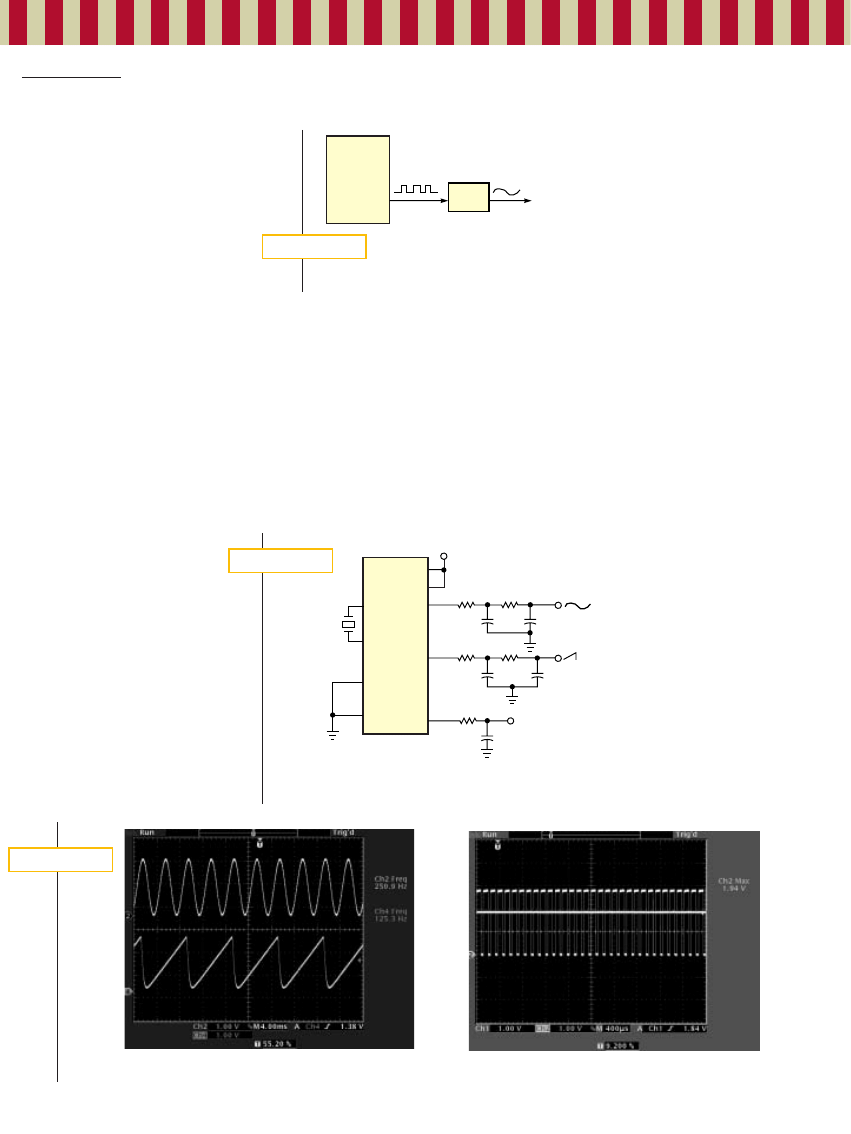
ter is an analog signal (Figure 1). If you
build a PWM DAC in this manner, its
resolution is equivalent to the resolution
of the PWM signal you use to create the
DAC. The PWM output signal requires
a frequency that is equivalent to the up-
date rate of the DAC, because
each change in PWM duty cycle
is the equivalent of one DAC sample. The
frequency the PWM timer requires de-
pends on the required PWM signal fre-
quency and the desired resolution. The
required frequency is F
CLOCK
⫽F
PWM
⫻2
n
,
where F
CLOCK
is the required PWM-timer
frequency, F
PWM
is the PWM-signal fre-
quency, and n is the desired DAC reso-
lution in bits.
Figure 2 depicts a circuit that delivers
a 250-Hz sine wave, a 125-Hz ramp, and
a dc signal. The desired sampling rate is
8 kHz (32 samples for each sine-wave cy-
cle (16
⫻ oversampled), and 64 samples
for each ramp cycle (32
⫻ oversampled)).
These figures result in a required PWM-
signal frequency of 8 kHz and a
required PWM clock fre-
quency of 2.048 MHz. It is
usually best for the PWM signal
frequency to be much higher than
the desired bandwidth of the sig-
nals to be produced. Generally, the
higher the PWM frequency, the
lower the order of filter required
and the easier it is to build a suit-
able filter. This design uses Timer
B of the MSP430 in 16-bit mode
and in “up” mode, in which the
counter counts up to the contents
of capture/compare register 0
(CCR0) and then restarts at zero.
CCR0 is loaded with 255, thereby
giving the counter an effective 8-bit
length. You can find this register and oth-
ers in a DAC demonstration program for
the MSP430 microcontroller. You can
download the program from the Web ver-
sion of this Design Idea at www.edn.com.
CCR1 and output TB1 produce the
sine wave. CCR2 and TB2 generate the
ramp, and CCR3 and TB3 yield the dc
value. For each output, the output mode
is the reset/set mode. In this mode, each
output resets when the counter reaches
the respective CCRx value and sets when
the counter reaches the CCR0 value. This
scheme provides positive pulses equiva-
lent to the value in CCRx on each re-
spective output. If you use the timer in 8-
bit mode, the reset/set output mode is
unavailable for the PWM outputs be-
cause the reset/set mode requires CCR0.
The timer’s clock rate is 2.048 MHz. Fig-
ure 3 shows the sine and ramp wave-
forms. The sine wave in this example uses
32 samples per cycle. The sample values
are in a table at the beginning of the pro-
gram. A pointer points to the next value
in the sine table, so that, at the end of
each PWM cycle, the new value of the
sine wave is written to the capture/com-
pare register of the PWM timer.
The ramp in this example does not re-
quire a table of data values. Rather, the
ramp simply increments the duty cycle
for each cycle of the PWM signal until it
reaches the maximum and then starts
over at the minimum duty cycle. This
gradual increase in PWM-signal duty cy-
cle results in a ramp voltage
when the signal passes through
a filter. You control the dc lev-
el by simply setting and not
changing the value of the
PWM-signal duty cycle. The dc
level is directly proportional to
the duty cycle of the PWM sig-
nal. Figure 2 shows the recon-
struction filters used for each
signal in this example. The fil-
ter for the ac signals is a sim-
ple two-pole, stacked-RC filter,
which is simple and has no ac-
tive components. This type of
filter necessitates a higher sam-
pling rate than would be re-
112
edn | September 5, 2002
www.edn.com
ideas
design
MSP430F149IPM
DV
CC
V
CC
AV
CC
AV
SS
DV
SS
P4.1/TB1
P4.2/TB2
P4.3/TB3
XIN
XOUT/TCLK
32,768 Hz
R
1
2k
R
2
1M
C
1
0.1
F
0.1
F
0.05
F
C
2
200 pF
2k
1M
200 pF
330k
DC
F i g u r e 2
A microcontroller and some passive filters produce a sine wave, a
ramp, and a dc signal.
The microcontroller’s PWM timer produces an ac signal (a) and a dc signal (b) of a sine wave and a ramp with 8-bit resolution.
F i g u r e 3
(a)
(b)
MSP430
MICRO-
CONTROLLER
PWM
OUTPUT
ANALOG
FILTER
F i g u r e 1
A PWM signal passing through a filter yields
and analog signal.
114
edn | September 5, 2002
www.edn.com
ideas
design
quired if the filter had a higher order.
With the type of filter shown in Fig-
ure 2, you should use at least a 16
⫻
oversampling rate.
The filter yields its best response
when R
2
⬎⬎ R
1
. Also, setting the cut-
off frequency too close to the band-
width edge causes a fair amount of at-
tenuation. To reduce the amount of
attenuation in the filter, set the cutoff
frequency above the bandwidth edge
but much lower than the frequency of
the PWM signal. The filter for the dc
value serves for charge storage rather
than ac-signal filtering. Therefore, it
uses a simple, single-pole RC filter.
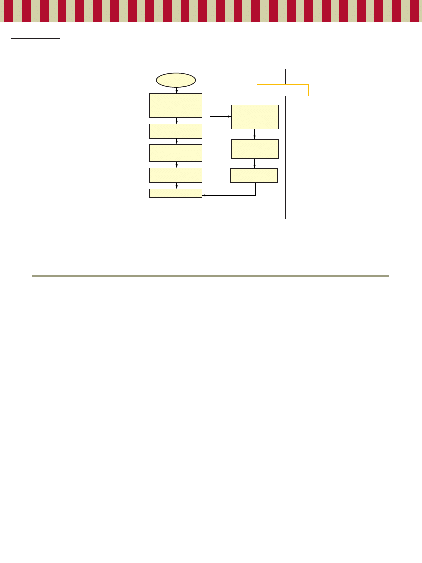
Figure 4 shows the software flow for
the DAC. After a reset, the routine
stops the watchdog timer, configures
the output ports, and sets up the clock
system. Next, the software calls a delay to
allow the 32,768-Hz crystal to stabilize to
calibrate the DCO (digitally controlled
oscillator).
Next, the routine calls the calibration
routine to set the operating frequency to
2.048 MHz. After the DCO calibration,
the program sets up Timer_B, CCR1 and
CCR2 for PWM generation and then
starts the timer. Finally, the MSP430
goes into low-power mode
0 (LPM0) to conserve pow-
er. The CPU wakes up to handle
each CCIFG0 interrupt from the
PWM timer and then re-enters
LPM0. (See references 1, 2, and 3
for more information on the DCO
and the MSP430 family.)
References
1. MSP430x13x/14x data sheet,
Texas Instruments document SLAS-
272.
2. MSP430x1xx Family User’s
Guide, Texas Instruments docu-
ment SLAU049.
3. “Controlling “the DCO of the
MSP430x11x,” Texas Instruments
document SLAA074.
Is this the best Design Idea in this
issue? Select at www.edn.com.
RESET
DISABLE WATCHDOG
TIMER, INITIALIZE I/O
PORTS, AND SET UP
CLOCK SYSTEM
CALL DELAY LOOP FOR
CRYSTAL STABILIZATION
CALL SOFTWARE
FREQUENCY-LOCK LOOP
FOR DCO STABILIZATION
SET UP TIMER_B AND
START PWM GENERATION
ENTER LPMO
INCREMENT AN AND
SINE-TABLE POINTER
AND MOVE NEW
VALUE TO CCR1
INCREMENT AN AND
RAMP VALUE AND
MOVE TO CCR2
RETURN FROM
INTERRUPT
TIMER_B
CCIFGO
INTERRUPT
This software flow diagram shows how the PWM timer
generates the sine and ramp signals.
F i g u r e 4
Wyszukiwarka
Podobne podstrony:
Converting Signal Strength Percentage to dBm Values
ECP Alchemy of the Heart How to Give and Receive More Love [OCR]
Jak wypełnić formularz Claim to an Employment Tribunal
Germany The answer to an old Question
Interfacing a 4x4 keyboard to an AT91 uC
ECP Alchemy of the Heart How to Give and Receive More Love [OCR]
Slide Ngôn Ngữ Lập Trình Tính Toán Fortran Trần Thùy Dương, 71 Trang
ĐHMO Lập Dự Toán Xây Dựng Cơ Bản Ths Lương Văn Cảnh, 21 Trang
KC 01 01 Công Nghệ Cứng Hóa Các Thuật Toán Mật Mã (NXB Hà Nội 2004) Nguyễn Hồng Quang, 71 Trang
tda7000 fm receiver
How to Process Goods Received
2003 Is coming to an Eng 2003 Zbliża się do inż
Message to an Alien Keith Laumer
7 Things You Must Do to Add Muscle, Gain Weight, and Increase Strength
A Permanent Solution to Internal Displacement An Assessment of the Van Action Plan for IDPs
NLP for Beginners An Idiot Proof Guide to Neuro Linguistic Programming
50 Common Birds An Illistrated Guide to 50 of the Most Common North American Birds
Zizek, Slavoj Looking Awry An Introduction to Jacques Lacan through Popular Culture
więcej podobnych podstron