UTC 7106
CMOS IC
UTC
UNISONIC TECHNOLOGIES CO., LTD.
1
QW-R502-018,B
3 1/2 DIGIT, LCD DISPLAY, A/D
CONVERTERS
DESCRIPTION
The UTC 7106 is a high performance, low power,
3 1/2 digit A/D converter. Included are seven segment
decoders, display drivers, a reference, and a clock.
The UTC 7106 is designed to interface with a liquid
crystal display (LCD) and includes a multiplexed
backplane drive.
The UTC 7106 bring together a combination of high
accuracy, versatility, and true economy. It features
auto zero to less than 10μV, zero drift of less than 1
μ
V/℃,input bias current of 10pA (Max),and rollover
error of less than one count. True differential inputs
and reference are useful in all system, but give the
designer an uncommon advantage when measuring
load cells, strain gauges and other bridge type
transducers. Finally, the true economy of single power
supply operation, enables a high performance panel
meter to be built with the addition of only 10 passive
components and a display.
FEATURES
*Guaranteed Zero Reading for 0V Input on All Scales
*True Polarity at Zero for Precise Null Detection
*1pA Typical Input Current
*True Differential Input and Reference, Direct Drive
LCD Display
*Low Noise-Less Than 15μVp-p
*On Chip Clock and Reference
*Low Power Dissipation-Typically Less Than 10mW
*No Additional Active Circuits Required
*Enhanced Display Stability
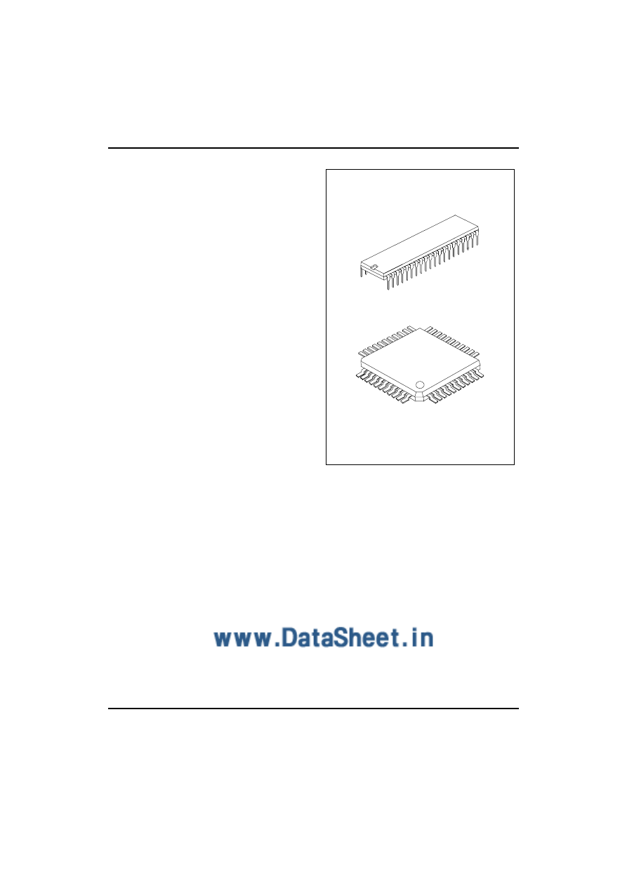
DIP-40
QFP-44-0.8
UTC 7106
CMOS IC
UTC
UNISONIC TECHNOLOGIES CO., LTD.
2
QW-R502-018,B
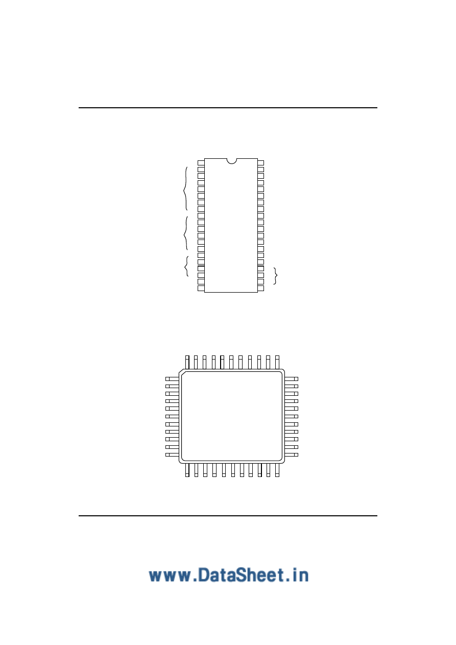
PIN CONFIGURATIONS
1
2
3
4
5
6
7
8
9
10
11
12
13
14
15
16
17
18
19
20
40
39
38
37
36
35
34
33
32
31
30
29
28
27
26
25
24
23
22
21
DIP- 40
V+
D1
C1
B1
A1
F1
G1
E1
D2
C2
B2
A2
F2
E2
D3
B3
F3
E3
(1000) AB4
POL
(MINUS)
OSC 1
OSC 2
OSC 3
TEST
REF HI
REF LO
C
REF
+
C
REF
-
COMMON
IN HI
IN LO
A-Z
BUFF
INT
V-
G2(10 s)
,
C3
A3
G3
BP
(100 s)
,
NC
G2
C3
A3
G3
BP
POL
AB4
E3
F3
B3
A1 F1 G1 E1 D2 C2 B2 A2 F2 E2 D3
B1
C1
D1
V+
OSC 1
OSC 2
NC
OSC 3
TEST
NC
NC
REF HI
REF LO
C
REF
+
C
REF
-
COMMON
IN HI
IN LO
A-Z
BUFF
INT
V-
1
2
3
4
5
6
7
8
9
10
11
12 13 14 15 16 17 18 19 20 21 22
33
32
31
30
29
28
27
26
25
24
23
44 43 42 41 40 39 38 37 36 35 34
(1 s)
,
(10 s)
,
(100 s)
,
QFP - 44
UTC 7106
CMOS IC
UTC
UNISONIC TECHNOLOGIES CO., LTD.
3
QW-R502-018,B
ABSOLUTE MAXIMUM RATINGS
(Ta=25℃)
PARAMETER SYMBOL
RATINGS
UNIT
Supply Voltage (V+ ~ V-)
V
DD
15 V
Analog Input Voltage (Either Input) (Note 1)
V
I,ANG
V+ ~ V-
V
Reference Input Voltage (Either Input)
V
I,REF
V+ ~ V-
V
Operating Temperature Range
T
OP
0 ~ +70
℃
THERMAL INFORMATION
PARAMETER SYMBOL
RATINGS
UNIT
Thermal Resistance (Tyical, Note 2)
DIP-40
QFP-44
θ
JA
50
75
(
°C/W)
Maximum Junction Temperature
T
J
150
°C
Maximum Storage Temperature Range
T
STG
-65 ~ +150
°C
Maximum Lead Temperature (Soldering 10s) (QFP-44 only)
T
LOAD
300
°C
Note 1: Input voltages may exceed the supply voltages provided the input current is limited to ±100μA.
Note 2: θ
JA
is measured with the component mounted on a low effective thermal conductivity test board in free air.
See Tech Brief TB379 for details.
ELECTRICAL CHARACTERISTICS
(Note 3)
PARAMETER SYMBOL
TEST
CONDITIONS
MIN
TYP
MAX
UNIT
SYSTEM PERFORMANCE
Zero Input Reading
R
Z
V
IN
=0.0V, Full Scale=200mV
-000.0
±
000.0 +000.0
Digital
Reading
Ratiometric Reading
R
R
V
IN
=V
REF
, V
REF
=100mV 999
999/1000
1000
Digital
Reading
Rollover Error
E
R
-V
IN
=+V
IN
≒
200mV
Difference in Reading for
Equal Positive and Negative
Inputs Near Full Scale
±
0.2
±
1
Counts
Linearity L
Full Scale=200mV or Full
Scale=2V Maximum Devi-
ation from Best Straight Line
Fit (Note 5)
±
0.2
±
1
Counts
Common Mode Rejection Ratio
CMRR
V
CM
=1V,V
IN
=0V,
Full Scale=200mV(Note 5)
50
μ
V/V
Noise V
N
V
IN
=0V,Full Scale=200mV
(Peak-To-Peak Value Not
Exceeded 95% of Time)
15
μ
V
Leakage Current Input
I
L
V
IN
=0(Note 5)
1
10
pA
Zero Reading Drift
D
ZR
V
IN
=0, 0℃ ~ 70℃ (Note 5)
0.2
1
μ
V/℃
Scale Factor Temperature
Coefficient
Φ
T,S
V
IN
=199mV, 0℃ ~ 70℃,
(Ext.Ref.0ppm/℃) (Note 5)
1
5
ppm/℃
End Power Supply Character V+
Supply Current
I
EP
V
IN
=0
1.0 1.8 mA
COMMON Pin Analog Common
Voltage V
COM
25kΩ Between Common
and Positive Supply (With
Respect to +Supply)
2.4 3.0 3.2 V
UTC 7106
CMOS IC
UTC
UNISONIC TECHNOLOGIES CO., LTD.
4
QW-R502-018,B
PARAMETER SYMBOL
TEST
CONDITIONS
MIN
TYP
MAX
UNIT
Temperature Coefficient of Analog
Common
Φ
T,A
25kΩ Between Common
and Positive Supply (With
Respect to +Supply)
80
ppm/℃
DISPLAY DRIVER
Peak-To-Peak Segment Drive
Voltage
Peak-To-Peak Backplane Drive
Voltage
V
D,PP
V+ ~ V-=9V(Note 4)
4
5.5
6
V
Note 3: Unless otherwise noted, specifications apply to the UTC 7106 at T
a
=25℃, f
CLOCK
=48kHz, UTC 7106 is
tested in the circuit of Figure 1.
Note 4: Back plane drive is in phase with segment drive for”off”segment,180 degrees out of phase for”on”
segment .Frequency is 20 times conversion rate. Average DC component is less than 50mV.
Note 5: Not tested, guaranteed by design.
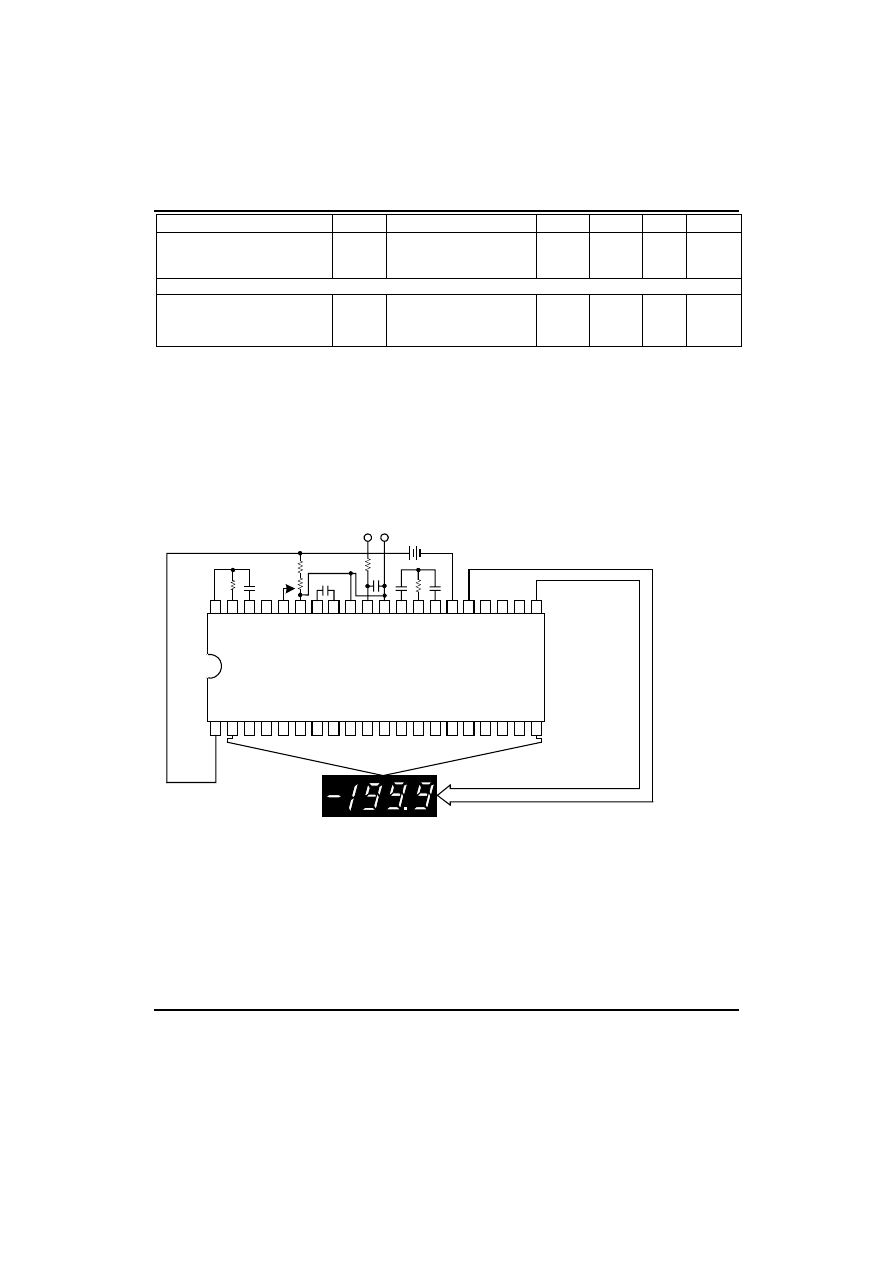
TYPICAL APPLICATIONS AND TEST CIRCUITS
(LCD DISPLAY COMPONENTS SELECTED FOR 200mV FULL SCALE)
1
2
3
4
5
6
7
8
9
10
11
12
13
14
15
16
17
18
19
20
21
22
23
24
25
26
27
28
29
30
31
32
33
34
35
36
37
38
39
40
V+
D1
C1
B1
A1
F1
G1
E1
D2
C2
B2
A2
F2
E2
D3
B3
F3
E3
AB4
POL
OSC 1
OSC 2
OSC 3
TEST
RE
F HI
RE
F L
O
C
REF
+
C
REF
-
COM
IN HI
IN LO
A-
Z
BU
FF
INT
V-
G2
C3
A3
G3
BP
UTC 7106
DISPLAY
R3
C4
R1
R4
C1
R5
C5
IN
+ -
C2 R2 C3
DISPLAY
C1=0.1μF
C2=0.47μF
C3=0.22μF
C4=100pF
C5=0.02μF
R1=24kΩ
R2=47kΩ
R3=91kΩ
R4=1kΩ
R5=1MΩ
+ -
9V
DESIGN INFORMATION SUMMARY SHEET
*OSCILLATOR FREQUENCY
fosc=0.45/RC
C
OSC
>50pF, R
OSC
>50kΩ
f
OSC
(Typ)=48kHz
*OSCILLATOR PERIOD
t
OSC
=RC/0.45
*INTEGRATION CLOCK FREQUENCY

UTC 7106
CMOS IC
UTC
UNISONIC TECHNOLOGIES CO., LTD.
5
QW-R502-018,B
f
CLOCK
=f
OSC
/4
*INTEGRATION PERIOD
t
INT
=1000×(4/f
OSC
)
*60/50Hz REJECTION CRITERION
t
INT
/t
60Hz
or t
INT
/t
50Hz
=Integer
*OPTIMUM INTEGRATION CURRENT
I
INT
=4μA
*FULL SCALE ANALOG INPUT VOLTAGE
V
INFS
(Typ)=200mV or 2V
*INTEGRATE ESISTOR
R
INT
= V
INFS
/ I
INT
*
INTEGRATE CAPACITOR
C
INT
=(t
INT
)(I
INT
)/ V
INT
*INTEGRATOR OUTPUT VOLTAGE SWING
V
INT
=(t
INT
)(I
INT
)/ C
INT
*VINT MAXIMUM SWING
(V- + 0.5V)<V
INT
<(V+ - 0.5V), V
INT
(Typ)=2V
*DISPLAY COUNT
COUNT=1000×V
IN
/V
REF
*CONVERSION CYCLE
t
CYC
=t
CLOCK
×
4000
t
CYC
=t
OSC
×
16,000
When f
OSC
=48kHz, t
CYC
=333ms
*COMMON MODE INPUT VOLTAGE
(V- + 1V)<V
IN
<(V+ - 0.5V)
*AUTO-ZERO CAPACITOR
0.01μF<C
AZ
<1μF
*REFERENCE CAPACITOR
0.1μF<C
REF
<1μF
*V
COM
Biased between Vi and V-
*V
COM
≒
V+ - 2.8V
Regulation lost when V+ to V- <≒6.8V
If V
COM
is externally pulled down to (V+ to V-)/2, the V
COM
circuit will turn off.
*POWER SUPPLY: SINGLE 9V
V+ - V- =9V
UTC 7106
CMOS IC
UTC
UNISONIC TECHNOLOGIES CO., LTD.
6
QW-R502-018,B
V
GND
≒
V+ - 4.5V
Digital supply is generated by internal parts.
*DISPLAY: LCD
Type: Direct drive with digital logic supply amplitude.
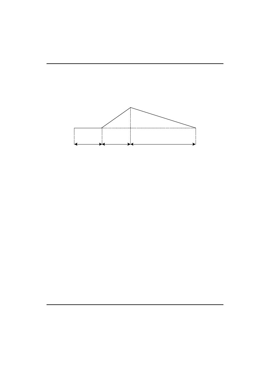
TYPICAL INTEGRATOR AMPLIFIER OUTPUT WAVEFORM (INT PIN)
DE-INTEGRATE PHASE
0 - 1999 COUNTS
SIGNAL INTEGRATE
PHASE FIXED
1000 COUNTS
AUTO ZERO PHASE
(COUNTS)
2999-1000
TOTAL CONVERSION TIME=4000 × t
CLOCK
=16,000 × tosc
DETAILED DESCRIPTION
ANALOG SECTION
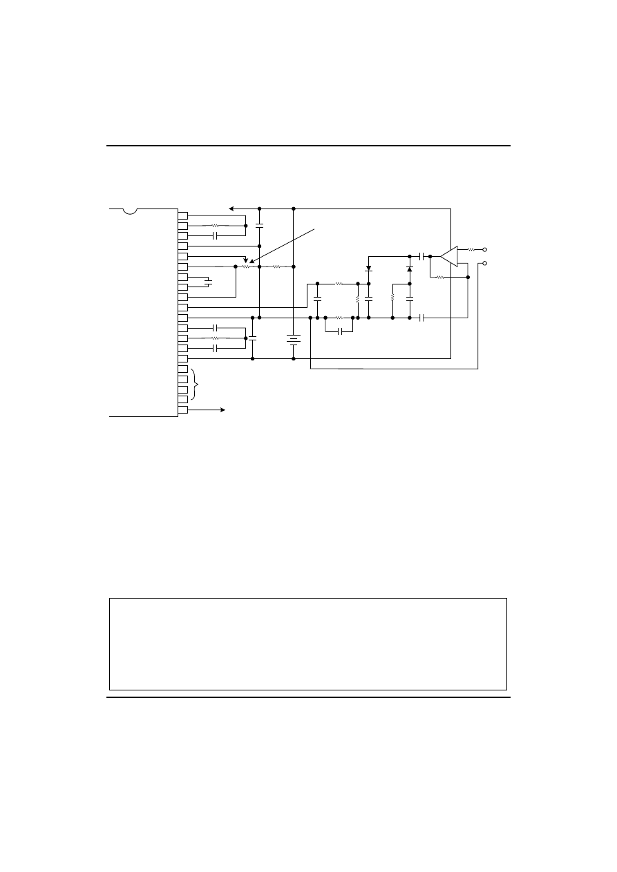
Figure 1 shows the Analog Section for the UTC 7106. Each measurement cycle is divided into three phases.
They are(1) auto-zero(A-Z), (2)signal integrate (INT)and (3)de-integrate(DE).
AUTO-ZERO PHASE
During auto-zero three things happen. First, input high and low are disconnected from the pins and internally
shorted to analog COMMON. Second, the reference capacitor is charged to the reference voltage. Third, a feedback
loop is closed around the system to charge the auto-zero capacitor C
AZ
to compensate for offset voltages in the
buffer amplifier, integrator, and comparator. Since the comparator is included in the loop, the A-Z accuracy is limited
only by the noise of the system. In any case. the offset referred to the input is less than 10μV.
SIGNAL INTEGRATE PHASE
During signal integrate, the auto-zero loop is opened, the internal short is removed, and the internal input high
and low are connected to the external pins. The converter then integrates the differential voltage between IN HI and
IN LO for a fixed time. This differential voltage can be within a wide common mode range: up to 1V from either
supply. if, on the other hand, the input signal has no return with respect to the converter power supply, IN LO can be
tied to analog COMMON to establish the correct common mode voltage. At the end of this phase, the polarity of the
integrated signal is determined.
DE-INTEGRATE PHASE
The final phase is de-integrate, or reference integrate. Input low is internally connected to analog COMMON and
input high is connected across the previously charged reference capacitor. Circuitry within the chip ensures that the
capacitor will be connected with the correct polarity to cause the integrator output to return to zero. The time required
for the output to return to zero is proportional to the input signal. Specifically the digital reading displayed is:
DISPLAY COUNT=1000( V
IN
/ V
REF
).
DIFFERENTIAL INPUT
The input can accept differential voltages anywhere within the common mode range of the input amplifier, or
specifically from 0.5V below the positive supply to 1V above the negative supply. In this range, the system has a
CMRR of 86dB typical. However, care must be exercised to assure the integrator output does not saturate. A worst
UTC 7106
CMOS IC
UTC
UNISONIC TECHNOLOGIES CO., LTD.
7
QW-R502-018,B
case condition would be a large positive common mode voltage with a near full scale negative differential input
voltage. The negative input signal drives the integrator positive when most of its swing has been used up by the
positive common mode voltage. For these critical applications the integrator output swing can be reduced to less
than the recommended 2V full scale swing with little loss of accuracy. The integrator output can swing to within 0.3V
of either supply without loss of linearity.
DIFFERENTIAL REFERENCE
The reference voltage can be generated anywhere within the power supply voltage of the converter. The main
source of common mode error is a roll-over voltage caused by the reference capacitor losing or gaining charge to
stray capacity on its nodes. If there is a large common mode voltage, the reference capacitor can gain charge
(increase voltage) when called up to de-integrate a positive signal but lose charge (decrease voltage) when called
up to de-integrate a negative input signal. This difference in reference for positive or negative input voltage will give
a roll-over error. However, by selecting the reference capacitor such that it is large enough in comparison to the stray
capacitance, this error can be held to less than 0.5 count worst case. (See Component Value Selection)
COMMON
IN LO
30
32
31
V+
A-Z
INT
INT
A-Z AND DE(±)
V-
FIGURE 1. ANALOG SECTION
DE+
DE-
DE-
DE+
A-Z
A-Z
REF HI
REF LO
C
REF
+
STRAY
C
REF
34
36
35
33
28
1
2.8V
-
+
-
+
-
+
29
27
INT
A-Z
C
INT
C
AZ
INTEGRATOR
R
INT
V+
STRAY
C
REF
-
TO
DIGITAL
SECTION
A-Z
COMPARATOR
INPUT
LOW
-
+
N
INPUT
HIGH
6.2V
10 A
IN HI
μ
BUFFER
ANALOG COMMON
This pin is included primarily to set the common mode voltage for battery operation (UTC 7106) or for any system
where the input signals are floating with respect to the power supply. The COMMON pin sets a voltage that is
approximately 2.8V more negative than the positive supply. This is selected to give a minimum end-of-life battery
voltage of about 6V. However, analog COMMON has some of the attributes of a reference voltage. When the total
supply voltage is large enough to cause the zener to regulate(>7V), the COMMON voltage will have a low voltage
coefficient (0.001%/V), low output impedance (≒15Ω), and a temperature coefficient typically less than 80ppm/℃.
The UTC 7106, with its negligible dissipation, suffers from none of these problems. In either case, an external
reference can easily be added, as shown in Figure 1.
Analog COMMON is also used as the input low return during auto-zero and de-integrate. If IN LO is different from
analog COMMON, a common mode voltage exists in the system and is taken care of by the excellent CMRR of the
converter. However, in some applications IN LO will be set at a fixed known voltage(power supply common for
instance).In this application, analog COMMON should be tied to the same point, thus removing the common mode
voltage from the converter. The same holds true for the reference voltage. If reference can be conveniently tied to
analog COMMON, it should be since this removes the common mode voltage from the reference system.
Within the IC, analog COMMON is tied to an N-Channel FET that can sink approximately 30mA of current to hold
the voltage 2.8V below the positive supply (when a load is trying to pull the common line positive). However, there is
UTC 7106
CMOS IC
UTC
UNISONIC TECHNOLOGIES CO., LTD.
8
QW-R502-018,B
only 10μA of source current, so COMMON may easily be tied to a more negative voltage thus overriding the internal
reference.
Iz
6.8V
ZENER
V-
V+
V
REF HI
REF LO
UTC 7106
COMMON
REF LO
REF HI
UTC 7106
V
20kΩ
6.8kΩ
ICL8069
V+
1.2V
REFERENCE
FIGURE 2B.
FIGURE 2A.
FIGURE 2. USING AN EXTERNAL REFERENCE
TEST
The TEST pin serves two function. On the UTC 7106 it is coupled to the internally generated digital supply through
a 500Ω resistor. Thus it can be used as the negative supply for externally generated segment drivers such as
decimal points or any other presentation the user may want to include on the LCD display. Figures 3 and 4 show
such an application. No more than a 1mA load should be applied.
The second function is a “lamp test”. When TEST is pulled high (to V+) all segments will be turned on and the
display should read ”1888”. The TEST pin will sink about 15mA under these conditions.
CAUTION: In the lamp test mode, the segments have a constant DC voltage (no square-wave) . This may burn the
LCD display if maintained for extended periods.
V+
TO LCD
BACKPLANE
1MΩ
TO LCE
DECIMAL
POINT
21
37
TEST
BP
UTC 7106
FIGURE 3. SIMPLE INVERTER FOR
FIXED DECIMAL POINT
V+
TEST
UTC 7106
BP
DECIMAL
POINT
SELECT
TO LCD
DECIMAL
POINTS
CD4030
GND
V+
FIGURE 4. EXCLUSIVE "OR" GATE FOR
DECIMAL POINT DRIVE
DIGITAL SECTION
Figure 5 show the digital section for the UTC 7106, respectively. In the UTC 7106, an internal digital ground is
generated from a 6V Zener diode and a large P-Channel source follower. This supply is made stiff to absorb the
relative large capacitive currents when the back plane(BP) voltage is switchied. The BP frequency is the clock
frequency divided by 800. For three readings/sec, this is a 60Hz square wave with a nominal amplitude of 5V. The
UTC 7106
CMOS IC
UTC
UNISONIC TECHNOLOGIES CO., LTD.
9
QW-R502-018,B
segments are driven at the same frequency and amplitude and are in phase with BP when OFF, but out of phase
when ON. In all cases negligible DC voltage exists across the segments.
LCD PHASE DRIVER
7
SEGMENT
DECODE
7
SEGMENT
DECODE
7
SEGMENT
DECODE
LATCH
1000 s
COUNTER
,
100 s
COUNTER
,
10 s
COUNTER
,
1 s
COUNTER
,
BACKPLANE
÷
200
LOGIC
CONTROL
÷
4
FROM COMPARATOR OUTPUT
*
THREE INVERTERS ONE INVERTER SHOWN FOR CLARITY
CLOCK
40
39
38
OSC 1
OSC 2
OSC 3
FIGURE 5. DIGITAL SECTION
V
TH
=1V
26
37
6.2V
500Ω
TEST
V-
V+
1
21
TYPICAL SEGMENT OUTPUT
SEGMENT
OUTPUT
2mA
0.5mA
V+
INTERNAL DIGITAL GROUND
INTERNAL
DIGITAL
GROUND
*
a
b
a
b
g
f
e
c
d
a
b
g
f
e
c
d
a
b
g
f
e
c
d
TO SWITCH DRIVERS
SYSTEM TIMING
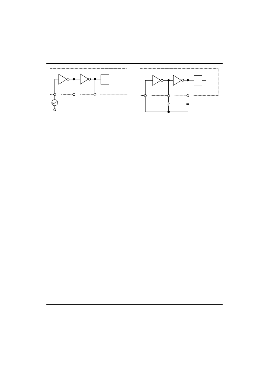
Figure 6 shows the clocking arrangement used in the UTC 7106. Two basic clocking arrangements can be used:
1. Figure 6A. An external oscillator connected to pin 40.
2. Figure 6B. An R-C oscillator using all three pins.
The oscillator frequency is divided by four before it clocks the decade counters. It is then further divided to form
the three convert-cycle phases. These are signal integrate (1000 counts), reference de-integrate(0 to 2000 counts)
and auto-zero(1000 ~ 3000 counts). For signals less than full scale. auto-zero gets the unused portion of reference
de-integrate. This makes a complete measure cycle of 4,000 counts (16,000 clock pulses) independent of input
voltage. For three readings/second, an oscillator frequency of 48kHz would be used.
To achieve maximum rejection of 60Hz pickup, the signal integrate cycle should be a multiple of 60Hz. Oscillator
frequencies of 240kHz, 120kHz, 80kHz, 60kHz, 48kHz, 40kHz, 33 1/3kHz, etc should be selected. For 50Hz
rejection, Oscillator frequencies of 200kHz, 100kHz, 66 2/3kHz, 50kHz, 40kHz, etc would be suitable. Note that
40kHz (2.5 readings/second) will reject both 50Hz and 60Hz (also 400Hz and 440Hz).
UTC 7106
CMOS IC
UTC
UNISONIC TECHNOLOGIES CO., LTD.
10
QW-R502-018,B
40
39
38
TEST
CLOCK
INTERNAL TO PART
FIGURE 6A
40
39
38
RC OSCILLATOR
CLOCK
INTERNAL TO PART
FIGURE 6B
R
C
FIGURE 6. CLOCK CIRCUITS
÷
4
÷
4
COMPONENT VALUE SELECTION
Integrating Resistor
Both the buffer amplifier and the integrator have a class A output stage with 100μA of quiescent current. They
can supply 4μA of drive current with negligible nonlinearity. The integrating resistor should be large enough to
remain in this very linear region over the input voltage range, but small enough that undue leakage requirements are
not placed on the PC board. For 2V full scale, 470kΩ is near optimum and similarly a 47kΩ for a 200mV scale.
Integrating Capacitor
The integrating capacitor should be selected to give the maximum voltage swing that ensures tolerance buildup
will not saturate the integrator swing(approximately. 0.3V from either supply).In the UTC 7106, when the analog
COMMON is used as a reference, a nominal+2V fullscale integrator swing is fine. For three readings/second (48kHz
clock) nominal values for C
INT
are 0.22μF and 0.10μF, respectively. Of course, if different oscillator frequencies are
used, these values should be changed in inverse proportion to maintain the same output swing.
An additional requirement of the integrating capacitor is that it must have a low dielectric absorptiont to prevent
roll-over errors. While other types of capacitors are adequate for this application, polypropylene capacitors give
undetectable errors at reasonable cost.
Auto-Zero Capacitor
The size of the auto-zero capacitor has some influence on the noise of the system. For 200mV full scale where
noise is very important, a 0.47μF capacitor is recommended. On the 2V scale, a 0.047μF capacitor increases the
speed of recovery from overload and is adequate for noise on this scale.
Reference Capacitor
A 0.1μF capacitor gives good results in most applications. However, where a large common mode voltage exists
(i.e.,the REF LO pin is not at analog COMMON)and a 200mV scale is used, a larger value is required to prevent
roll-ovre error. Generally 1μF will hold the roll-over error to 0.5 count in this instance.
Oscillator Components
For all ranges of frequency a 91kΩ resistor is recommended and the capacitor is selected from the equation:
f= 0.45/RC For 48kHz Clock (3 Readings/sec), C=100pF.
Reference Voltage
The analog input required to generate full scale output (2000 counts) is: V
IN
=2V
REF
.Thus, for the 200mV and 2V
scale, V
REF
should equal 100mV and 1V, respectively.However,in many applications where the A/D is connected to
a transducer, there will exist a scale factor other than unity between the input voltage and the digital reading. For
instance, in a weighing system, the designer might like to have a full scale reading when the voltage from the
UTC 7106
CMOS IC
UTC
UNISONIC TECHNOLOGIES CO., LTD.
11
QW-R502-018,B
transducer is 0.662V. Instead of dividing the input down to 200mV, the designer should use the input voltage directly
and select V
REF
=0.341V. Suitable values for integrating resistor and capacitor would be 120kΩ and 0.22μF. This
makes the system slightly quieter and also avoids a divider network on the input.
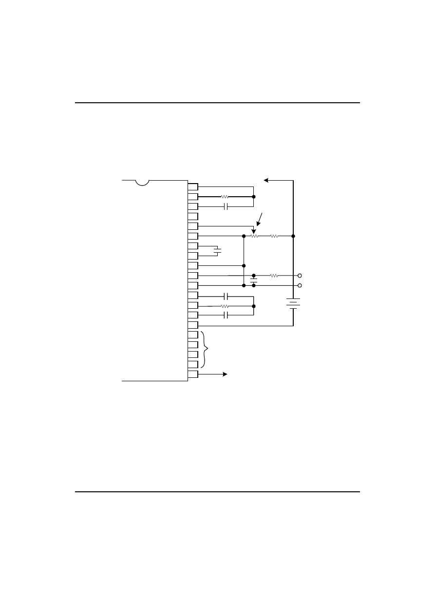
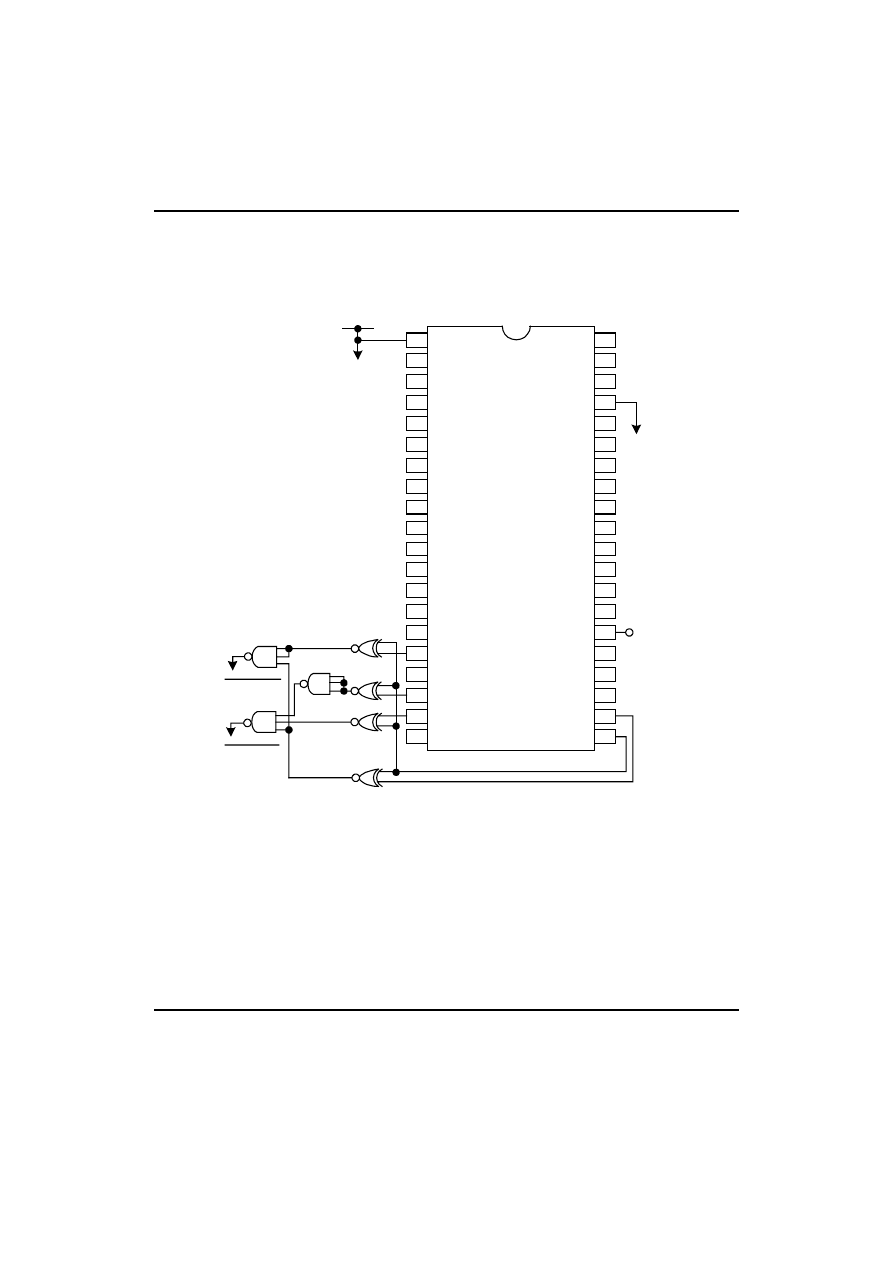
TYPICAL APPICATIONS
The UTC 7106 may be used in a wide variety of configurations. The circuits which follow show some of the
possibilities, and serve to illustrate the exceptional versatility of these A/D converters.
OSC 1
OSC 2
OSC 3
TEST
REF HI
REF LO
C
REF
C
REF
COMMON
IN HI
IN LO
A-Z
BUFF
INT
V -
G2
C3
A3
G3
BP
40
39
38
37
36
35
34
33
32
31
30
29
28
27
26
25
24
23
22
21
TO PIN 1
91kΩ
100pF
0.1μF
0. 01μF
0. 47μF
1kΩ
22kΩ
1MΩ
47kΩ
0. 22μF
SET V
REF
=100mV
9V
IN
+
-
+
-
TO DISPLAY
TO BACKPLANE
Values shown are for 200mV full scale,3 readings/sec.,floating
supply voltage(9V battery).
FIGURE 7. USING THE INTERNAL REFERENCE
UTC 7106
CMOS IC
UTC
UNISONIC TECHNOLOGIES CO., LTD.
12
QW-R502-018,B
TYPICAL APPLICATIONS (Continued)
OSC 1
OSC 2
OSC 3
TEST
REF HI
REF LO
C
REF
C
REF
COMMON
IN HI
IN LO
A-Z
BUFF
INT
V -
G2
C3
A3
G3
BP
40
39
38
37
36
35
34
33
32
31
30
29
28
27
26
25
24
23
22
21
TO PIN 1
91kΩ
100pF
0.1μF
0. 01μF
0. 047μF
25kΩ 24kΩ
1MΩ
470kΩ
0. 22μF
SET V
REF
=100mV
IN
+
-
TO DISPLAY
FIGURE 8. RECOMMENDED COMPONENT VALUES
FOR 2V FULL SCALE
V+
V-
UTC 7106
CMOS IC
UTC
UNISONIC TECHNOLOGIES CO., LTD.
13
QW-R502-018,B
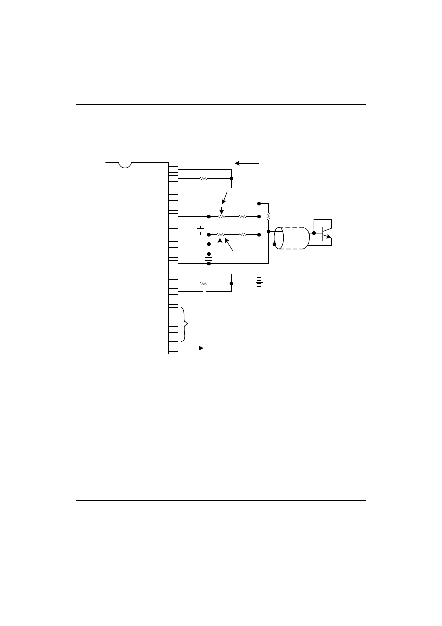
TYPICAL APPLICATIONS (Continued)
OSC 1
OSC 2
OSC 3
TEST
REF HI
REF LO
C
REF
C
REF
COMMON
IN HI
IN LO
A-Z
BUFF
INT
V -
G2
C3
A3
G3
BP
40
39
38
37
36
35
34
33
32
31
30
29
28
27
26
25
24
23
22
21
TO PIN 1
91kΩ
100pF
0.1μF
0. 47μF
100kΩ 1MΩ
47kΩ
0. 22μF
SCALE
FACTOR
ADJUST
9V
TO DISPLAY
A sillicon diode-connected transistor has a temperature coefficient of about -2mV/
℃
.
Calibration is achieved by placing the sensing transistor in ice water and adjusting the
zeroing potentiometer for a 000.0 reading.The sensor should then be placed in boiling
water and the scale-factor potentiometer adjusted for a 100.0 reading
FIGURE 9. USED AS A DIGITAL CENTIGRADE THERMOMETER
0.01μF
100kΩ 220kΩ
22kΩ
ZERO
ADJUST
SILICON NPN
MPS 3704 OR
SIMILAR
TO BACKPLANE
UTC 7106
CMOS IC
UTC
UNISONIC TECHNOLOGIES CO., LTD.
14
QW-R502-018,B
TYPICAL APPLICATIONS (Continued)
1
2
3
4
5
6
7
8
9
10
11
12
13
14
15
16
17
18
19
20
21
22
23
24
25
26
27
28
29
30
31
32
33
34
35
36
37
38
39
40
V+
D1
C1
B1
A1
F1
G1
E1
D2
C2
B2
A2
F2
E2
D3
B3
F3
E3
AB4
POL
OSC1
OSC2
OSC3
TEST
REF HI
REF LO
CREF
CREF
COMMON
IN HI
IN LO
A-Z
BUFF
INT
V-
G2
C3
A3
G3
BP
V+
TO
LOGIC
V
DD
O/RANGE
U/RANGE
CD4077
V-
TO
LOGIC
GND
FIGURE 10. CIRCUIT FOR DEVELOPING UNDERRANGE AND
OVERRANGE SIGNAL FROM UTC 7106 OUTPUTS
UTC 7106
CMOS IC
UTC
UNISONIC TECHNOLOGIES CO., LTD.
15
QW-R502-018,B
TYPICAL APPLICATIONS (Continued)
OSC 1
OSC 2
OSC 3
TEST
REF HI
REF LO
C
REF
C
REF
COMMON
IN HI
IN LO
A-Z
BUFF
INT
V -
G2
C3
A3
G3
BP
40
39
38
37
36
35
34
33
32
31
30
29
28
27
26
25
24
23
22
21
TO BACKPLANE
TO DISPLAY
47kΩ
0.47μF
0.22μF
10μF
9V
+
-
100pF
(FOR OPTIMUM BANDWIDTH)
SCALE FACTOR ADJUST
(V
REF
=100mV FOR AC TO RMS)
1μF
470kΩ
4.3kΩ
10kΩ
1N914
10kΩ
1μF
100kΩ
+
-
2.2MΩ
5μF
AC IN
TO PIN 1
22kΩ
1kΩ
91kΩ
100pF
0.1μF
Test is used as a common-mode reference level to ensure compatiblity with most op amps.
CA3140
1μF
10μF
0.22μF
FIGURE 11. AC TO DC CONVERTER WITH UTC 7106
UTC assumes no responsibility for equipment failures that result from using products at values that
exceed, even momentarily, rated values (such as maximum ratings, operating condition ranges, or
other parameters) listed in products specifications of any and all UTC products described or contained
herein. UTC products are not designed for use in life support appliances, devices or systems where
malfunction of these products can be reasonably expected to result in personal injury. Reproduction in
whole or in part is prohibited without the prior written consent of the copyright owner. The information
presented in this document does not form part of any quotation or contract, is believed to be accurate
and reliable and may be changed without notice.
Wyszukiwarka
Podobne podstrony:
7106
ICL 7107 i ICL 7106
ne088, Ne088, NE 047 TERMOMETR -50° +150°C LCD/ICL 7106
icl7107 7106
7106
7106
7106
7106
7106
praca magisterska 7106
ICL 7107 i ICL 7106
7106
więcej podobnych podstron