
MICROACTUATORS AND THEIR TECHNOLOGIES
E. Thielicke, E. Obermeier
Technical University of Berlin, Microsensor & -actuator Technology Center (MAT)
TIB 3.1, Gustav-Meyer-Allee 25, 13355 Berlin, Germany,
Phone: +49 30 314 72 769, Fax: +49 30 314 72 603,
email: oberm@mat.ee.tu-berlin.de, URL: http://mat.ee.tu-berlin.de
Abstract
This paper gives a brief overview of microactuators, focussing on devices made
by microfabrication technologies which are based on silicon processes like
photolithography, etching, thin film deposition etc. These technologies enable the
minaturization of electrical devices as well as micromechanisms and
microactuators. They can be batch fabricated on large area silicon substrates and
represent the smallest available in a vast field of actuators.
Mentioning the activation principles and the three main fabrication technologies:
bulk micromachining, surface micromachining and moulding, the paper focusses
on devices, which made their way into industrial applications or prototypes. The
far most developed MEMS (micro electro-mechanical systems) are found in
micro-fluidic systems (printheads, microvalves and -pumps) and micro-optical
systems (micromirrors, -scanners, -shutters and -switches). They can be
combined with microelectronics and microsensors to form an integrated on-chip
or hybrid-assembled system. Other MEMS-actuators like microgrippers,
microrelays, AFM heads or data storage devices, are promising devices for
future medical, biological and technical applications like minimal invasive surgery
or the vast field of information storage and distribution.

Introduction
For more than a decade microactuators have been developed using structures
and technologies based on those of microsensors and semiconductor fabrication
technology. Silicon still plays a leading role, not only as the electrical, but also as
the mechanical material [1].
The first devices have been simple mechanical resonant structures agitated by
electrostatical forces to detect humidity by analysing the resonant frequency [2]
and bulk micromachined valves and membrane pump prototypes using
piezoelectric and thermopneumatic forces [3, 4]. Later in the 80s more
sophisticated mechanical elements like springs, cranks, gears and other novel
micromechanical structures were presented to facilitate for the fist time rotational
microdynamics and complex micromachines [5-7].
The same physical laws and material constants govern the micro as well as the
macro world. Scaling macro-actuators down to micro-actuators shifts the
influence of individual parameters on the total system dramatically. Compared to
macro- or mini-actuators, microactuators allow completely new mechanical
designs. Volumes and masses for example decrease superproportionally
(cubically) compared to lengths. Scaling down mechanical systems leads to stiff
and comparatively ligthweight structures with high shock resistance. But in
addition one has to keep in mind that thin films, that are used for the batch
fabrication of microactuators, often have different material properties compared
to bulk materials including intrinsic stress induced by high temperature
processing and deposition [8, 9].
In 1988 the first IC-processed rotational electrostatic micromotor has been
shown [10]. But these early, small (
?
?
100 µm) and weak machines found no
way into the application field. Since then there has been done much work to
improve the actuators and some applications were found.

Singular problems like friction [11, 12] or sticking [13] are still not yet solved to
everyone's satisfaction. Because of the small sizes (bearing clearance in the sub-
µm range) and limitations in technological feasibility, no ball bearings exist like in
the macroscopic world, although there are made some efforts to use
electromagnetic, electrostatic, gas flow or fluidic bearings [14, 15].
If zero-friction-motion is required, e.g. positioning tables without hysteresis, the
movable parts have to be suspended by elastic beams or membranes. Until today
frictionless motion is implemented in the predominant proportion of all MEMS
(micro electro-mechanical systems) which are conceived for a technical
application in order to avoid mechanical wear and to enable thus long life and
high economical benefit.
Microfluidic devices like micropumps and microvalves are todays furthest
developed microactuators and sold on the market in high volumes. They are used
for example in µ-TAS (micro total analysis systems) or nano-litre dosing systems
[16]. Inkjet print heads are the most common and most well-known microfluidic
devices, although only few people expect such MEMS in a non-returnable ink
cartridge in their desktop bubble jet printer [17].
Apart from these microfluidics there are further areas of application for MEMS in
microoptics and electronic systems like (optical) switches and relays, scanners,
(mirror based) displays, variable capacitances and inductances with an enormous
market in (optical) computer networks and telecommunications [18, 19]. Data
storage systems as well as AFM and STM tools use microactuators in their head
carriers to achieve ultra high density recording / scanning [20]. Mostly
piezoelectric microactuators are used for the piggy back actuators of hard disk
drives, because they have a sufficiently rapid response and sufficient force to
allow improved control of the servo system which maintains the recording sensor
over the center of the track [21].

Actuation Principles
The scaling has not only consequences for the mechanical design but also for the
actuation of microactuators. The right choice of the actuation principle is
dependent on the structural dimensions, the technology, the response time, the
force or torque as a function of displacement and the maximum power
consumption as well [22].
Force can be generated following two main principles:
1) external forces which are generated in the space between stationary and
moving parts using thermopneumatic [23] and electrochemical [24] effects,
electrostatic [25] and magnetic fields [26] or
2) inner forces which use special materials having intrinsic actuation capapilities
including piezoelectric [27], thermomechanical [28], shape memory [29],
electro- and magnetostrictive effects [30].
Although nearly every permutation of activation principle and device has been
tried, only a few have been leaving the research laboratories. See in addition
Table 1 for typical MEMS devices together with their activation principle, which
have been succesfully realized and implemented in industrial applications or
prototypes.

actuation principle
typical MEMS devices
piezoelectric
micropump [54]
microvalve [31]
HDD servo system [21]
electrostatic
micromotor (shutter) [56]
microshutter [32]
micromirror [68]
microscanner [61]
microrelay [33, 34]
electromagnetic
microrelay [35]
micropump, -valve [36]
thermomechanic
microvalve [37]
microgripper [65]
thermopneumatic
phase conversion
micropump [23, 38]
microvalve [39]
inkjet printhead [51]
shape memory
microvalve [40]
fiber-optic switch [41]
Table 1: MEMS devices and their activation principle.
Electrostatical actuation is the mostly applied principle combining versatility and
simple technology. It needs neither additional elements like coils or cores, nor
special materials like shape-memory-alloys or piezoelectric ceramics. Above that
the electrostatical actuation draws its force from the relation of surface to spacing
and not from the relation of volume to spacing, i.e. it is less affected by scaling
and more favourable for VLSI actuators [42].
Rotational and linear micromotors are often found to be a key part of
micromechanical systems allowing them to perform physical functions. They can
be used in x-y-stages, for aperture controling in microphotonics, driving forces
for micro-relays, micro-mirrors and micro-grippers. They also initialise
mechanical systems, carry out on-chip assembling and rise pop-up structures.
The most commonly used activation principle for micromotors is the
electrostatic field between the plates of capacitors including comb drives [43],
curved electrodes [44], scratch [45], wobble [46], linear stepping [47] and side
drives with synchronous and asynchronous operation [48].
See in addition the Figures 1 to 6 for the operating principles and some SEM
photographs of the devices.
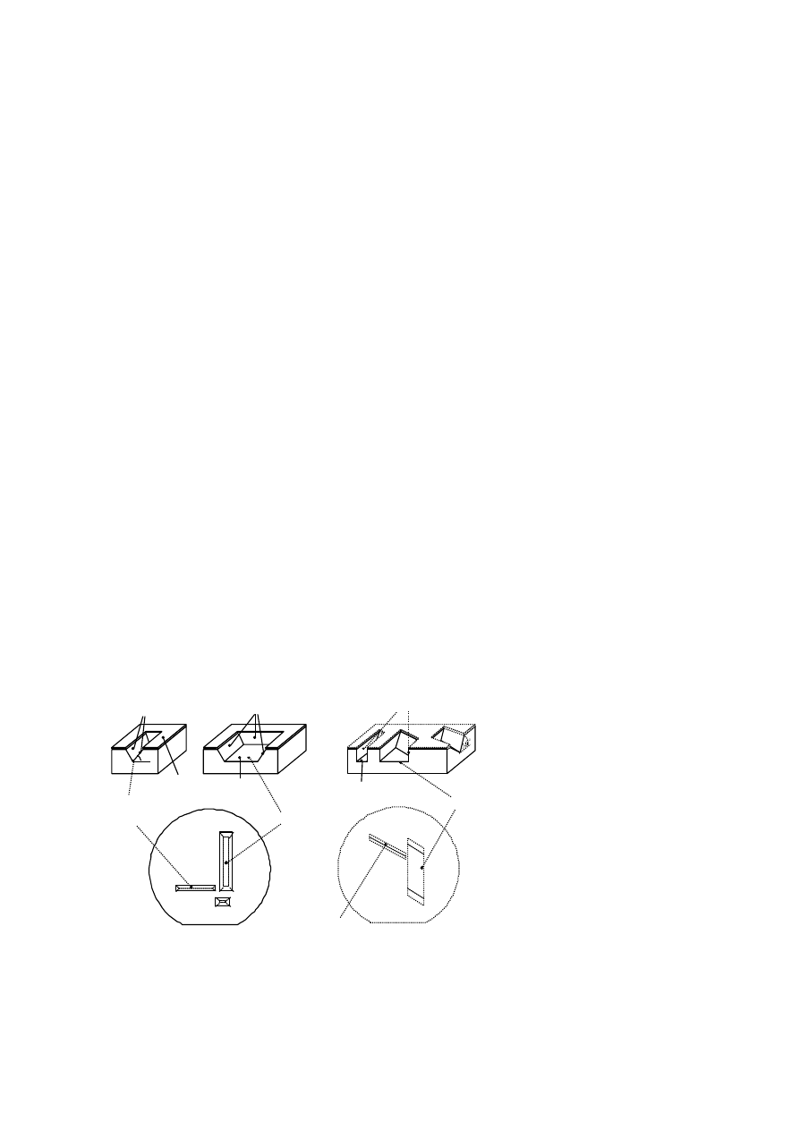
beam
anchor
moving poles
stator poles
U
a)
b)
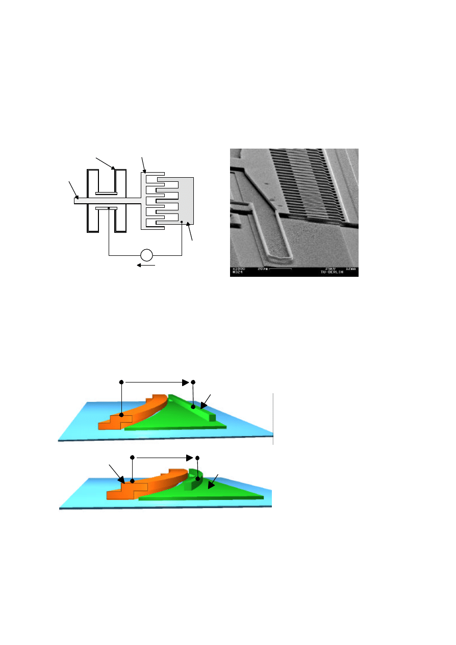
Fig. 1: a) Schematical view of a comb drive linear actuator. The anchor is
suspended by beams. Electrostatical forces pull it towards the right. b) SEM
photograph of the comb drive.
U = 0 V
U > 0 V
ground electrode
beam electrode
stator electrode
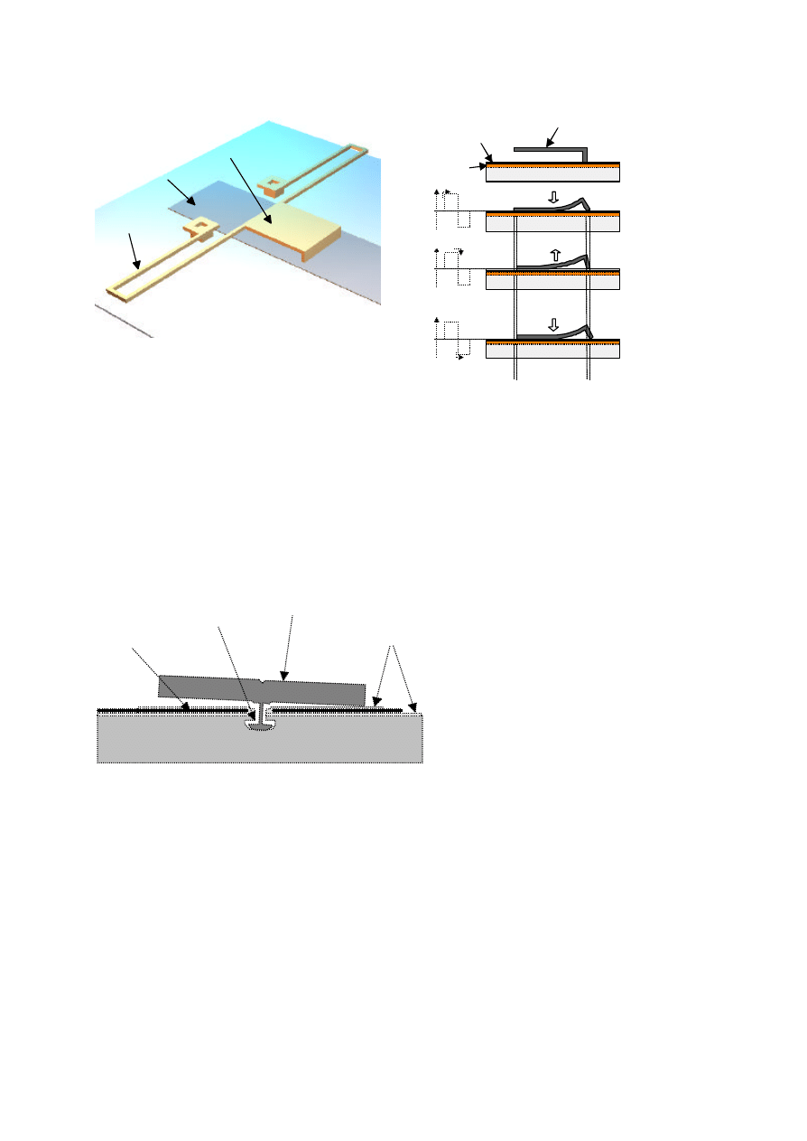
Fig. 2: Curved electrode actuator in resting position (upper half of the figure).
The feather beam is clamped on one side to the ground electrode and forms itself
the mobile electrode. If a voltage is applied between the stator and the feather
beam electrode, the beam is "rolled up" by the stator electrode (lower half of the
figure) [44].
beam
movable electrode
isolating layer
counter electrode
a)
?
x
isolation
movable
electrode
Si substrate
?
x
0
U
0
U
0
U
counter
electrode
b)
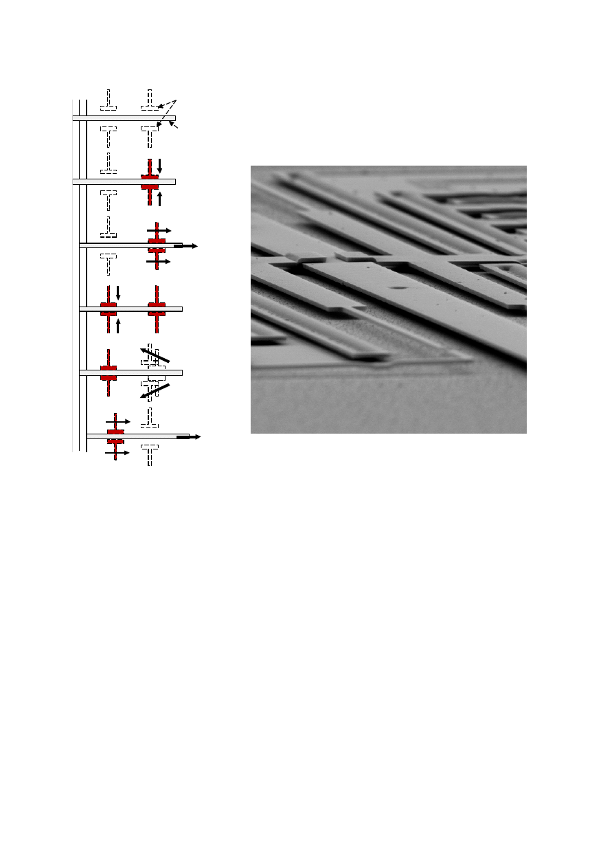
Fig. 3 : Scratch drive actuator (a) and its operating principle (b). It moves
forward by parallel plate capacitor and frictional forces with the substrate surface
[45].
stator
electrodes
bearing
isolating layers
rotor
Si substrate
Fig. 4 : Schematical cross section of a wobble micromotor. The rotor is rolling
on the isolation layer like a wobbling gyroscope. It is less affected by wear,
because the moving part of the bearing is rolling as well (and less sliding) in the
bearing shell [46].
Greifer
Anker
a)
b)
Fig. 5: a) The four finger linear stepping motor uses grip arms that can be moved
in two dimensions: perpendicular to the anchor to hold it by frictional forces and
parallel to shift it for- or backwards. b) SEM photograph of the central beam and
the grip arms [47].
U
1
1'
1
1
1
1
1
1'
1'
1
1'
1
1
1
1
1
1'
1'
2
2
2
2
2
2
2'
2'
2'
U
U
guide ways
sliding anchor
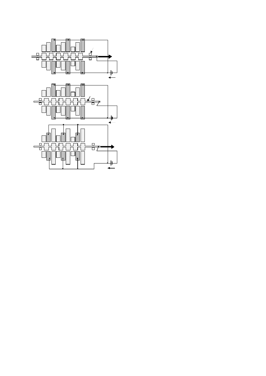
Fig. 6: Synchronous side drive motor. The stator poles and the sliding anchor are
charged antipodally and move the anchor by tangential electrostatical forces as
long as the electrode faces remain shifted. When the faces stand opposite to each
other, the next stator electrodes are charged and so on [48].
Asynchronous operation does not only use attracting, but also repulsive forces.
The sliding anchor is made of high resistive and the stator poles are made of low
resistive material (e.g. undoped and doped polysilicon). After the anchor is
completely charged and the charges stand opposite to each other, the potentials
of the stator poles are quickly inverted. The charges in the low resistive anchor-
material remain (they relaxe very slowly) and the anchor is pulled due to attractive
forces of the neighbouring stator poles and additionally pushed because of the
repulsive forces, which are due to the opposite stator poles. The asynchronous
motor leads to a better efficiency compared to synchronous operation mode.
Technology and Applications for Microactuators
Starting out from the three main technologies for microactuators some examples
and applications will be presented. These technologies are: bulk-micromachining,
surface-micromachining and moulding technologies including classical
electroplating, the HEXSIL and the LIGA processes. Additionally processes are
used which are known from standart IC-fabrication.
Bulk Micromachining
Bulk micromachining has been dominated in the past by aqueous solutions like
KOH, TMAH and EDP. Due to the fact that {100} and {110} planes of single
crystal silicon are etched up to 100 times faster than {111} planes, anisotropically
etched grooves and membranes like the ones shown in Figure 7 can be realized in
a quite simple apparatus [49]. Nowadays it is also possible to etch silicon
anisotropically not dependent on the crystal orientation in DRIE-reactors. These
processes allow small structures (> 2 µm) to be etched with high aspect-ratios (>
15) and a very good anisotropy (> 99 %) [50].
(100)
{111}
54.7°
(100)- wafer
(110)- wafer
v-groove with 70,52°
opening angle
v-groove with
110° opening angle
{111}
{111}
(100)
(110)
trapezoidal grooves
u-groove
Fig. 7: Anisotropically etched structures in (100)- and (110)-oriented silicon
wafers. Planes with (111)-orientation are almost not etched by the KOH solution.
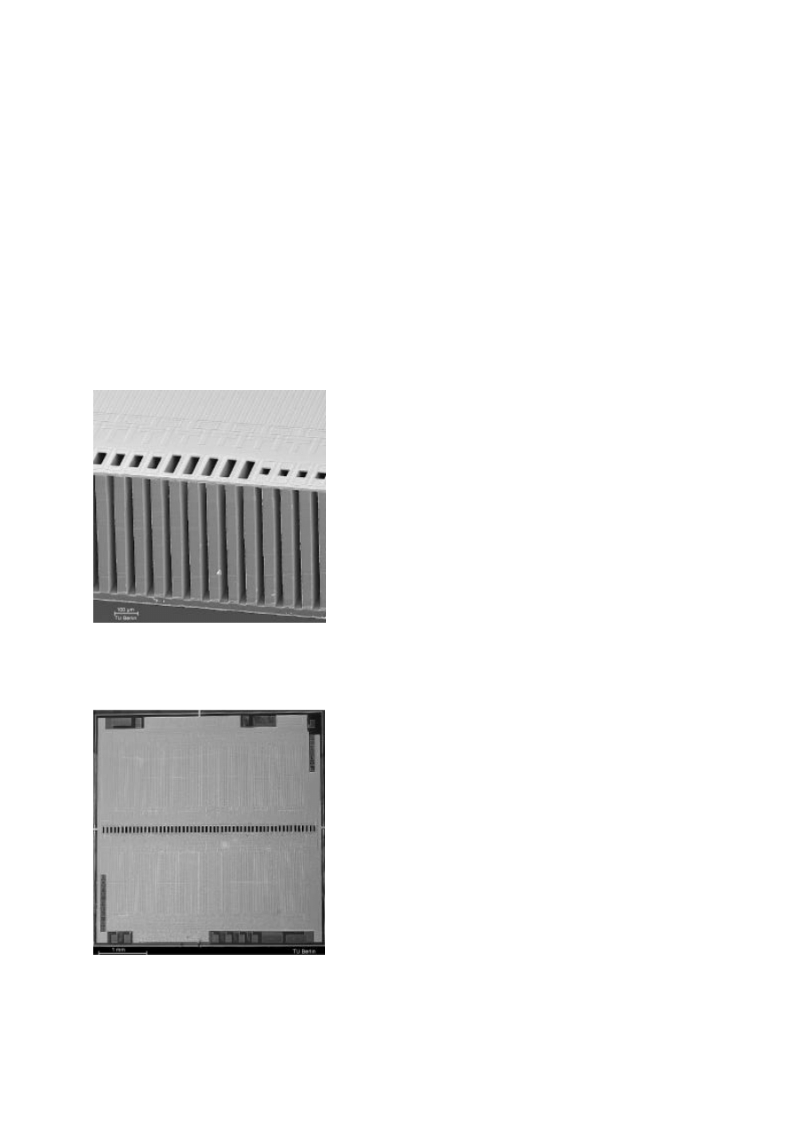
Fig. 8 shows silicon structures anisotropically etched by KOH that belong to a
micromachined inkjet printhead, often called bubble jet or drop-on-demand print
head wich can be seen in Figure 9. The inkjet print head combines micro-
mechanics, heating actuators, temperature sensors, channels and nozzles with a
smart CMOS circuit including signal processing [51]. The outside dimensions
amount to 4.9 x 4.0 mm² with nozzle dimensions of 20 x 40 µm². Droplet
velocities between 10 and 15 m / s and droplet masses between 60 and 110 ng
are meeting conventional inkjet printer requirements.
Fig. 8: Partial view of a cross sectional SEM image of bulk micromachined
nozzles and deep narrow grooves for the ink supply.
Fig. 9: Smart ink jet print head microsytem with 50 nozzles and CMOS circuit on
a single chip.
Other MEMS fabricated using bulk-micromachining technology, like valves and
micropumps have found there way into industrial applications since many years.
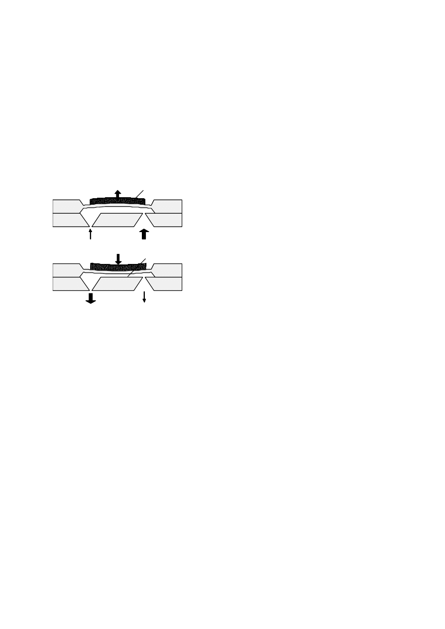
Figure 10 shows the schematical structure of a micropump with piezoelectric
actuation and bulk micromachined silicon diffusion valves. But also designs with
watertight and/or airtight valves and integrated or hybrid-assembled flow sensor
and control unit are available [52]. The flow rates range from single drops in the
sub nanolitre range up to several ml per minute. The substrates (glass + silicon or
silicon + silicon with intermediate glass layer) are anodically bonded, leading to a
stable covalent bond between both materials [53].
Si # 1
Si # 2
Si # 1
Si # 2
piezoelectric film
inlet B
inlet B
inlet A
inlet A
pump chamber
Fig. 10: Simple micropump design with piezoelectrically actuated membrane and
bulk micromachined silicon diffusion valves. The arrows explain the operating
principle in wich a big arrow pointing in or out the outlet means high flow and a
small arrow means weak flow. The sum of the flows leads to a transport of
liquid/gas from outlet B to A.
Figure 11 shows the Debiotech (Switzerland) micropump developed to be the
heart of an implantable drug infusion system [54]. The device is based on silicon
bulk micromachining, silicon pyrex (glass) anodic bonding. and piezoelectric
actuation. The pumping mechanism has been designed for maximum safety and
reliability together with high open-loop accuracy (±10%) in a low flow rate range
(0–100 µl/h). The overall size is 16 x 12 mm².
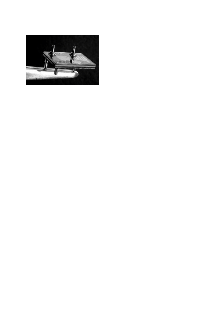
Fig. 11: Bulk micromachined, piezoelectric micropump [54].
Surface michromachining
Surface micromachining makes mainly use of polysilicon as the "active" material
(mechanically and electrically) and silicon-oxide as the sacrificial layer. Several
active and intermediate sacrificial layers can be grown one on top of each other
on a silicon wafer. Another possibilty is to use aluminium as the active and
organic compounds (polyimid, photoresist) as the sacrificial layer. The layers are
patterned by classical photolithographical processes and wet or plasma etch.
Finally the sacrificial layer(s) are etched away to release the structures [55].
Surface micromachined structures are always build upwards and remain on the
surface of the substrate during the whole fabrication process and in the
application. Figure 12 shows the main fabrication steps of a double clamped
beam (bridge) using surface micromachining technology.
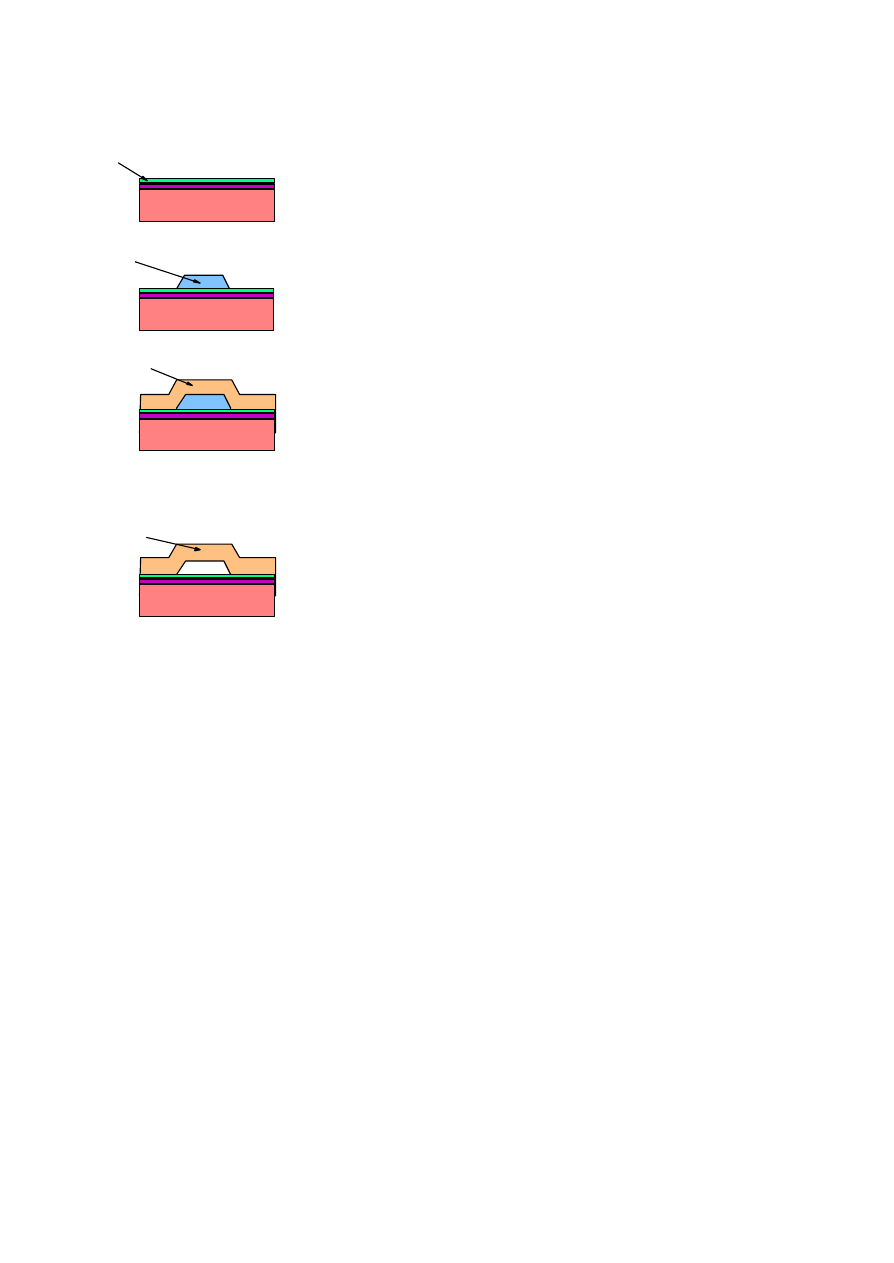
Si-Substrat
isolating layers
sacrificial layer
polysilicon
removing the sacrificial
layer leads to free-
standing structures
Fig. 12: Single layer surface micromachining process for fixed and movable
structures.
Even complicated mechanical components, like beams, guide ways, bearings,
hinges and locking mechanisms can be realized by choosing a suitable
combination of layers and their appropriate processing. Many of the micromotor
designs presented in chapter 2 have been realized using surface micromachining,
which leads necessarily to a multi layer surface micromachining process.
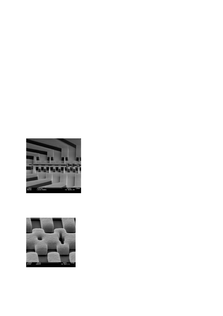
Figure 13 shows schematically the fabrication steps for an electrostatically driven
rotational micromotor with central bearing. The bearing clearance is only 400 nm.
The distance between stator and anchor poles amounts to 2 µm with a
polysilicon layer thickness of 2 µm. The Figures 14 and 15 show close-ups of
the central bearing and the poles.
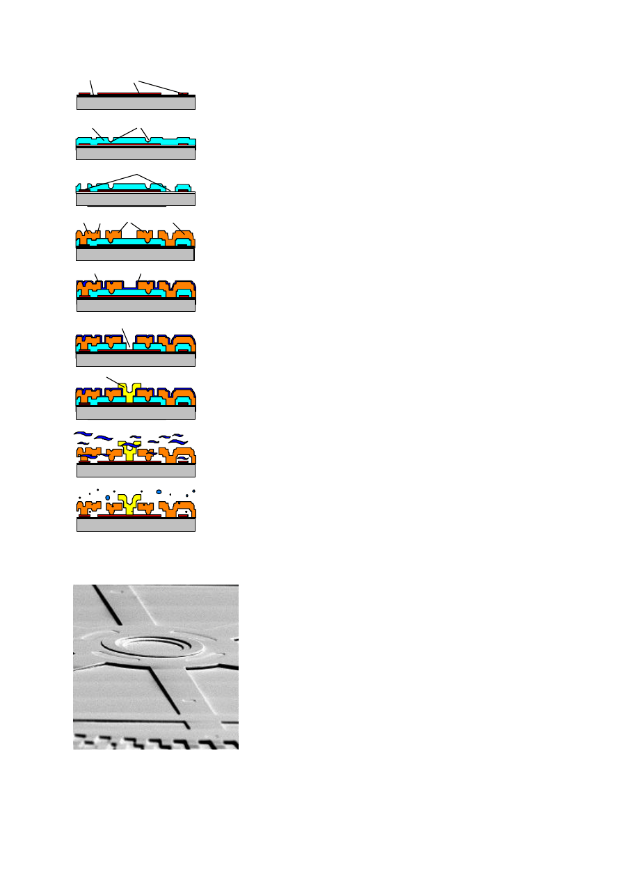
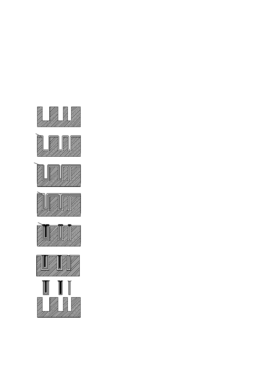
Si
isolation
poly-1 (phase lines)
Si
sacrificial layer
bushing moulds
Si
vias
3 4
step 1: definition of phase
lines by LPCV-deposition
and patterning of polysilicon
on an isolating Si N layer.
step 2: bushing moulds are
patterned by deposition of the
first sacrificial layer wich is
isotropically etched by HF.
step 3: vias are opened by
anisotropical etch to contact the
second poly layer with poly 1.
Si
2. sacrificial layer bearing clearance
Si
via for the bearing
Si
poly-2 stator rotor micro bridge
step 4: the rotor and stator
are patterned by deposition
of the second poly layer wich
is etched anisotropically in
a SF plasma.
step 5: a thin sacrificial oxide
layer is deposited to define
the bearing clearance.
step 6: vias are etched down
to poly 1 to connect poly 3 with
the phase lines.
Si
Si
poly-3 bearing
step 7: the bearing is realized
by patterning a third
polysilicon layer.
Si
step 8: removing the sacrificial
oxide in HF acid creates the
bridges and releases the rotor.
step 9: drying in a sublimation
process prevents the micro-
structures from sticking to the
substrate.
6
Fig. 13: Surface micromachining of rotational micromotors (cross section).
Fig. 14: SEM photograph of the central bearing of a surface micromachined
rotational actuator.
Fig. 15: SEM photograph of the driving poles of a surface micromachined
electrostatical micromotor. The poles are connected by polysilicon microbridges
(see arrow).
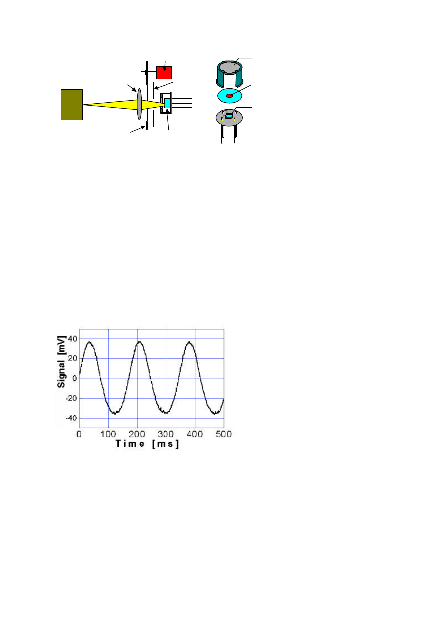
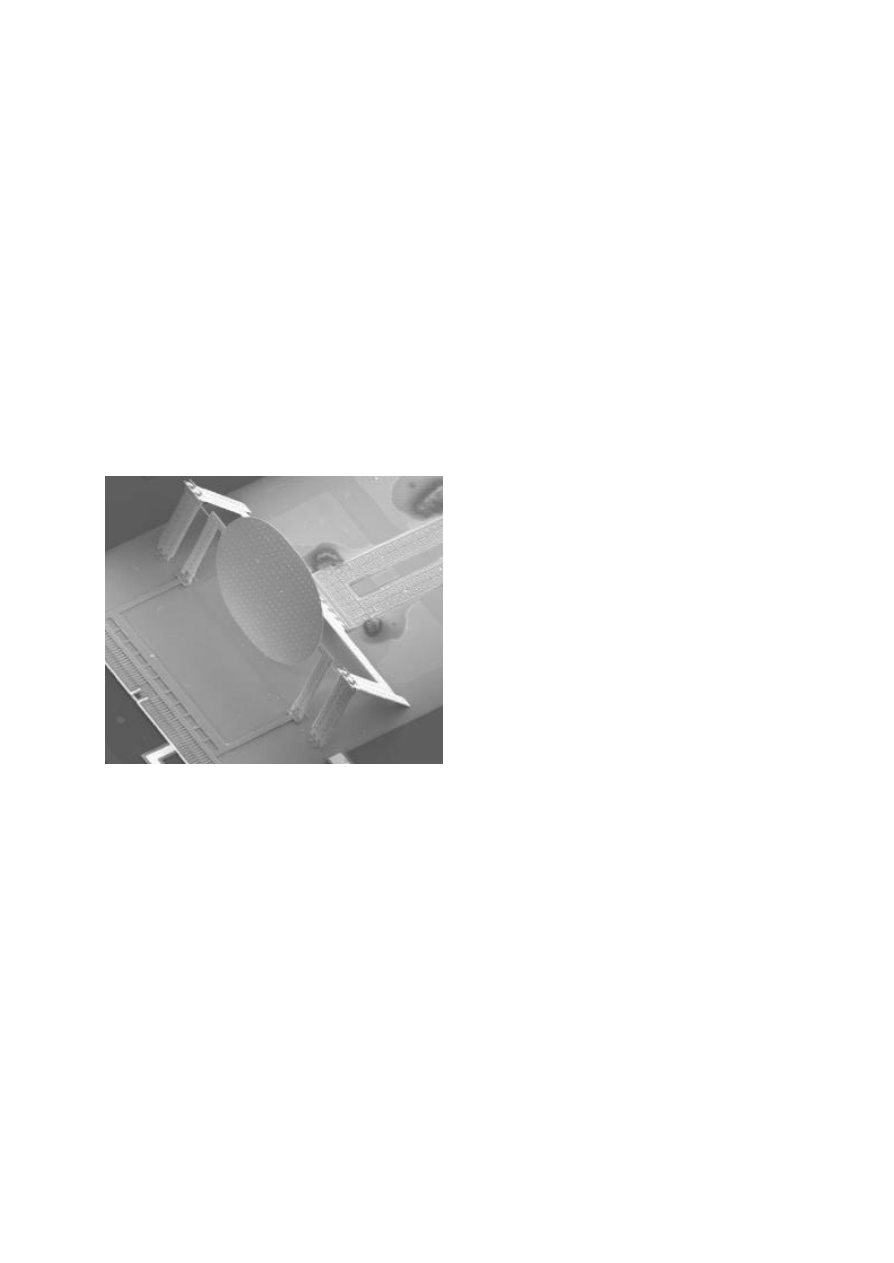
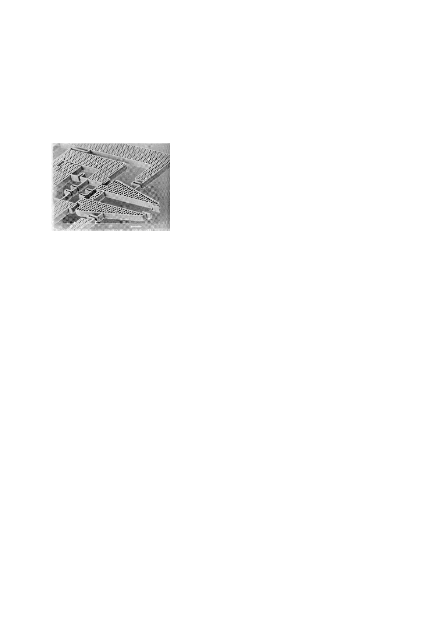
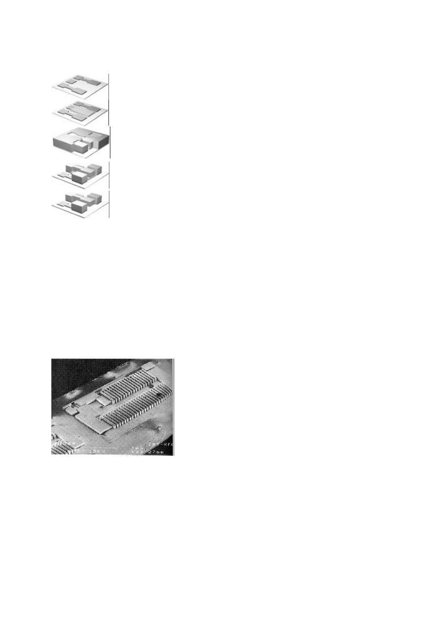
A SEM-photograph of the whole device can be seen in Figure 16. Figure 17
illustrates its application as a micro-shutter for the modulation of radiation in
optical or thermal detectors. The rotor diameter of the microshutter amounts to
between 800 µm and 1200 µm. An aperture of 100 x 200 µm² to 200 x 300 µm²
is etched from the backside of the substrate with bulk micromachining
technology. Parts of the rotor and the whole backside are coated with a thin gold
layer to reduce IR transmittance. The shutter is applied in a pyroelectric detector
with numbers of revolution ranging from 0 rpm up to 200 rpm. The minimum
driving voltage is 35 V [56].
Fig. 16: SEM-picture of the micro-shutter fabricated using surface (motor) and
bulk micromachining technology (aperture).
s h u t t e r d i s c
l e n s
p y r o e l e c t r i c
d e t e c t o r
a p e r t u r e
m o t o r
T = ?
lens
micro
shutter
pyroelectric
detector
a)
b)
Fig. 17: a) Conventional apparatus for a temperature radiation measurement unit
with pyroelectric detector, electromagnetic motor and chopper disk; b) its micro-
electro-mechanical counterpart which integrates the motor, the chopper disk and
the aperture hole in a single device contained together with the pyroelectric
detector in a single housing.
Pyroelectric detectors do only generate output signals when they have excitation
and refreshing cycles, i.e. when the radiation is chopped. Only 180 revolutions
(rpm) are necessary to achive an output signal like the one shown in Figure 18.
Fig. 18: Output signal of the pyroelectric detector when excited by heat radiation.
The radiation is modulated by a surface micromachined chopper turning 180
rpm.
The linear stepping microactuator presented in chapter 2, Figure 5 has an overall
dimension of 1 x 2 mm², yielding "high" forces (some 10 µN) and "large"
displacements (>100 µm) with an accuracy in the nm range wich are limited only
by the length of the central beam. Surface micromachined devices can be made
quite large in the lateral dimension (up to 4 mm²), but the maximum height
amounts to between 2 and 10 µm, beause the thicknesses of the layers are limited
[57, 58]. A way out offer pop-up-structures realized by hinges and connecting
rods [59]. Figure 19 shows a two axis micromirror for an optical scanner wich is
tilted by comb drives.
Fig. 19: SEM photograph of a pop-up micromirror [60, 61].
Moulding
Moulding processes can be devided into three main groups: classical
electroplating, LIGA and HEXSIL processes. All moulding technologies allow
high aspect ratios and a structure height of more than 100 µm, but the mechanical
structures are more simple and less diverse compared with surface micromaching
[62].
Electroplating
Classical electroplating technology is using photoresist or other photo-
structurable, organic materials for the female form of the structures. They are
deposited on various substrates with low resistivity or metal coating (starting
layer) [63]. After the moulds are patterned, metals like Au, Ni, Cu or alloys are
grown into the moulds by electrodeposition starting from the metal layer. Like
surface micromachining technology, sacrificial layers can be used to realize
bridges, suspending beams or sliding anchors. The structures are freed by
stripping the photoresist. Each mould can only be used once. Figures 20 and 21
show a partial view of a patterned photoresist mould and the gold structures after
the plating process and resist stripping took place.
Fig. 20: Partial view of a patterned photoresist mould for a syncronous mirco
linear actuator in gold electroplating technology.
Fig. 21: Partial view of the electroplated gold structures that were grown into the
mould shown in Fig. 20.
HEXSIL
The HEXSIL process was developed at UC Berkeley. It is using LPCVD-
processes (low-pressure chemical vapour deposition) and silicon moulds
fabricated by DRIE (deep reactive ion etching) of silicon wafers. The devices do
not remain on the substrate where they were fabricated, so that the moulds can
be used several times. Figure 22 shows the steps of HEXSIL processing.
step 1: DRIE (deep reactive ion etching)
of the female silicon mould.
step 2: LPCVD (low pressure chemical
vapour deposition) of the
sacrificial layer ( silicon oxide).
step 3: LPCVD of undoped polycrystalline
silicon as the isolation layer.
step 4: Deposition of in-situ doped
polycrystalline silicon for the
heating elements (thermo-
mechanical activation).
step 5: Plasma etch (dry etch) of the
polysilicon layers and
deposition of metal for the
electrical feed lines.
step 6: CMP (chemical mechanical
polishing) down to the sacrifical
oxide layer.
step 7: The structures are released by
removing the sacrificial oxide in
a HF solution.
Si
Oxid
undoped poly-silicon
doped poly-silicon
nickel
Si
Si
Si
Si
Si
Si
Fig. 22: Steps of the HEXSIL-process.
A SEM photograph of a HEXSIL micro-tweezer is to be seen in Figure 23. It is
actuated by thermomechanical forces and has an overall dimension of 2 mm x
1.4 mm x 80 µm. An application for micro-tweezers will be the handling and
assembling of microparts to build up microsystems with growing complexity
[64]. Another future operational area could be in the field of minimal invasive
surgery.
Fig. 23: Partial view of a micro-tweezer fabricated using the HEXSIL process
[65].
LIGA
The LIGA process [66] (RöntgentiefenLithographie, Galvanoformung &
Abformung = deep x-ray lithography, electroforming & moulding/embossing)
was developed at FZK (Forschungszentrum Karlsruhe, Germany). It starts with a
thick layer (up to several 100 µm) of PMMA (polymethylmethacrylate,
plexiglass) wich is deposited on a metal substrate. The structures are patterned
by parallel and high energy x-ray lithography. The gaps are filled up with metal
(Au, Cu, Ni, NiFe etc.) by electrodeposition. The electroforming process starts
on the metal substrate. Either the PMMA or the released metal structures can be
used as the female mould. Mass production of polymer, metal and even ceramic
microcomponents makes use of hot embossing and injection moulding.
Cantilever LIGA-structures can be realized by sacrificial layer etching (e.g.
titanium). Figure 24 shows the process steps of a suspended LIGA-
microstructure.
step 1: patterning of metal layer
on isolating substrate.
step 2: patterning of the sacrificial layer.
step 3: spin-on coating of the PMMA
(h > 100 µm), deep x-ray litho-
graphy and electroplating.
step 4: removal of the PMMA.
step 5: removal of the sacrificial layer.
Fig. 24: Process steps of a suspended structure using LIGA technology.
Figure 25 shows a SEM photograph of an electromagnetic micro-relay fabricated
using FeNi (permalloy) in the LIGA process. Many efforts are made to develop
µ-SMD compatible, fast switching low-power micro-relays for applications in
e.g. telecommunication and ATM (automated test equipment).
Fig. 25: SEM photograph of an electromagnetically actuated micro-relay
fabricated using the LIGA process [67].
A growing number of devices are fabricated using a mix of several technologies.
Often CMOS circuits are integrated to create a smart microsystem.
Microsensors, IC signal processing and microactuators are combined on a single
chip allowing the system to step into interaction with the environment.
Compatibility of processes plays an important role. Hot processes like surface
micromachining, diffusion or annealing have to be performed first. Bulk
micromachining processes are implemented last, because they are cold (60°C –
90 °C) and produce deep grooves with high aspect ratios that mostly do not
allow any further lithographical steps. Very complex microsystems have been
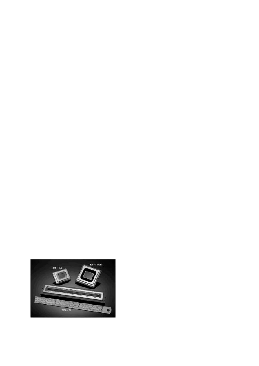
fabricated and brought to market like the Texas Instruments digital micromirror
device (DMD) pixel array shown in Figure 26. A schematical view of an
electrostatically driven mirror which is representing one single pixel is to be seen
in Figure 27. A light source illuminates the micromirror array in such a way that
the light beams are deflected either to the screen or not, depending on the tilting
state of the mirror (in plane or out of plane). Each pixel on the screen can thus be
switched on or off by actuating the appropriate mirror, leading to a digital image.
Using RGB light beams and three DMD arrays (or one DMD array together with
serial colour modulation) allow to screen a coloured image. The devices are used
in desktop digital light projectors, featuring up to 1280 x 1024 pixels. The
advantage compared to conventional technology is that a bright light source can
be used thus achieving a brightly shining image.
Fig. 26: Array of electrostatically actuated micromirrors for applications in color
projection displays [68].
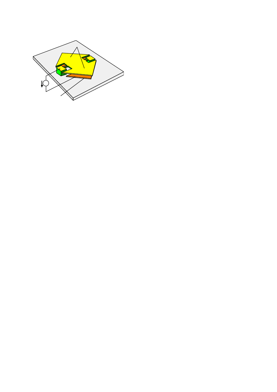
U
mirror = tilting electrode
ground electrode
Fig. 27: Schematical view of a micromirror with electrostatical actuation.
Conclusion
Micromachined actuators are no longer just designed in research laboratories to
show state of the art technology. Some applications have been found in the last
ten years and put to a rapidly growing market. However microsystem technology
is still in the initial phase of its development. The future of micro actuators will be
marked by new applications that have sophisticated requirements concercing
small size, low weight, low power consumption, high shock resistance and high
mechanical cut-off frequency. Already today first applications have been
implemented that would have been inconceivable with conventional techniques.
Microactuators cannot be designed just by scaling macro- or miniactuators and
the intention of researchers is not to replace conventional technology. They offer
new solutions for applications and enlarge the field of actuators, which will lead
to a coexistance of micro- and conventional actuators. It is clearly essential that
only micromachines will fit into small environments and that for example a small
manipulator can handle microobjets much more gently and dexterously than its
macro conterparts. With microactuators finer positioning in shorter response
time is possible than with macroscopic machines. Only a few statements can be
made in order to deceide about an actuation principle or microactuator design,
because their usefulness is strongly coupled to the application. It has been shown

that various types of actuation principles and different fabrication technologies
are available. They can be combined to achieve the required functionality, yield
and costs. Still a set of problems is unsolved. Friction, wear, sticking and fatigue
reduce the life time and reliability. Much more efforts will be required to
introduce new materials, designs and technological concepts to solve these and
future problems. The fusion of knowledge from many different disciplines is
essential for a well-balanced and accelerated growth of the microsystem
technology and will allow new applications in further technical, medical and
biological areas.

References
[1] Petersen K. Silicon as a mechanical material. Proc. IEEE. 1982; vol. 70: 420-
57.
[2] Howe RT. Resonant Microsensors. Transducers '87: 4th Int. Conf. Solid-
State Sensors and Actuators. 1987; 843-8.
[3] van Lintel H, van de Pol F, Bouwstra S. A Piezoelectric Micropump Based
on Micromachining of Silicon. Sensors and Actuators. 1988; 15: 153-7.
[4] Gravesen P, Branebjerg J, Fensen OS. Microfluidics - A Review. MME '93:
Micro Mechanics Europe, Workshop, Neuchatel Switzerland. 1993; 143-64.
[5] Fan LS, Tai Y-C, Muller RS. Pin joints, gears, springs, cranks and other
novel micromechanical structures. Trans. '87: 4th Int. Conf. S.-S. Sen. Act.
1987; 849-52.
[6] Muller RS. Microdynamics. Sens. Act. 1990; A 21: 1-8.
[7] Fujita H. Microactuators and Micromachines. Proc. IEEE. 1998; vol. 86, no.
8: 1721-32.
[8] Obermeier E. Material Property Data -A Key Issue for the Design of
Microsystems. Proc. of the Int. Symposium on Microsystems, Intelligent
Materials and Robots, Sendari Japan. 1995; 110-3.
[9] Maier-Schneider D, Köprülülü A, Ballhausen Holm S, Obermeier E. Elastic
peoperties and microstructure of LPCVD polysilicon films. J. Micromech.
Microeng. 1996; 6: 436-46.
[10] Fan LS, Tai Y-C, Muller RS. IC-processed electrostatic micromotors. Sens.
Act. 1989; vol. 20: 41-8.
[11] Lim MG, Chang JC, Schulz DP, Howe RT, White RM. Polysilicon
Microstructures to Characterize Static Friction. IEEE Micro Electro Mechanical
Systems; Napa Valley California USA. 1990; 82-8.
[12] Deng K, Ko H, Michal GM. A Preliminary Study on Friction Measurements
in Mems. Trans '91.: 6th Int. Conf. S.-S. Sens. Act. 1991; 213-16.
[13] Tas N, Sonnenberg T, Jansen H, Legtenberg R, Elwenspoek M. Stiction in
surface micromachining. J. Micromech. Microeng. 1996; 6: 385-97.
[14] Kumar S, Cho D, Carr W. Electric Levitation Bearings for Micromotors.
Transducer ´91: 6
th
International Conference on Solid-State Sensors and
Actuators. 1991; 882-5.
[15] Deng K, Ramanathan G, Mehregany M. Micromotor dynamics in lubricating
fluids. J. Micromach. Microeng. 1991; 4: 266-269.

[16] Papautsky I, Brazzle JD, Weiss RB, Ameel TA, Frazier AB. Parallel sample
manipulation using micromachined pipette arrays. Proc. SPIE: Microfluidic
Devices and Systems, Santa Clara California USA. 1998; vol. 3515: 104-14.
[17] Wehl W. Tintendrucktechnologie: Paradigma und Motor der
Mikrosystemtechnik (Inkjet technology: Paradigm and driving force of micro
system technology). F and M Feinwerktechnik Mikrotechnik Messtechnik,
Germany. 1995; Ch. 6 and 9 (in German).
[18] Zhou S, Sun X-Q, Carr W. A Micro Variable Inductor Chip Using MEMS
Relays. Trans. '97: 9
th
Int. Conf. S.-S. Sens. Act., Chicago USA. 1997; 1137-40.
[19] Walker SJ. Optics & MEMS: An Overview of Current Technology.
MOEMS '97: Int. Conf. on Optical MEMS and Their Applications. 1997; 179-
85.
[20] Lutwyche M, Andreoli C, Binnig G, Brugger J, Drechsler U, Häberle W,
Rohrer H, Rothuizen H, Vettiger P, Yaralioglu G, Quate C. 5 x 5 2D AFM
cantilever arrays a first step towards a Terabit storage device. Sens. Act. 1999; A
73: 89-94.
[21] Naniwa I, Nakamura S, Saegusa S, Sato K. Low Voltage Driven Piggy-Back
Actuator of Hard Disk Drives. IEEE MEMS, Orlando USA. 1999; 49-52.
[22] Benecke W. Silicon - Microactuators: Activation Mechanisms and Scaling
Problems. Trans. ´91: 6
th
Int. Conf. S.-S. Sens. Act. 1991; 46-9.
[23] van de Pol FCM, van Lintel HTG, Elwenspoek M, Fluitman JHJ. A
Thermopneumatic Micropump Based on Micro-engineering Techniques. Sens.
Act. 1990; vol. 21: 198-202.
[24] Böhm S, Olthius W, Bergveld P. An Electrochemically Actuated
Micropump for Use in a 'Push-Pull' Microdialysis Based In-Vivo Monitoring
System. Transducer ´99: 10
th
International Conference on Solid-State Sensors
and Actuators, Sendai Japan. 1999; 880-1.
[25] Trimmer WSN, Gabriel KJ, Mahadevan R. Slicon Electrostatic Motors.
Trans. '87: 4th Int. Conf. S.-S. Sens. Act. 1987; 857-60.
[26] Wagner B, Kreutzer M, Benecke W. Linear and Rotational Magnetic
Micromotors Fabricated Using Silicon Technology. Proc. IEEE Micro Electro
Mechanical Systems, Travemünde Germany. 1992; 183-9.
[27] Robbins WP, Polla DL, Tamagawa T, Glumac DE. Design of linear-motion
microactuators using piezoelectric thin films. J. Micromech. Microeng. 1991;
1(4): 247-52.
[28] Que L, Park J-S, Gianchandani YB. Bent-Beam Electro-Thermal Actuators
for High Force Applications. IEEE MEMS, Orlando USA. 1999; 31-6.

[29] Reynaerts D, Peirs J, Van Brussel H. An implantable drug-delivery system
based on shape memory alloy micro-actuation. Sens Act. 1997; A 61: 455-62.
[30] Quandt E; Seemann K. Fabrication and simulation of magnetostrictive thin-
film actuators. Sens. Act. 1995; A 50: 105-9.
[31] Roßberg R. Mikrodosierung für portable Flüüsigkeitsabgabesysteme.
Dissertation, Shaker Verlag, Aachen Germany. 1995.
[32] Lin J, Schlichting V, Obermeier E. Design and Fabrication of an
Electrostatically Driven Micro-Shutter. Trans '93: 7th Int. Conf. S.-S. Sens. Act.,
Yokohama Japan. 1993.
[33] Schlaak H, Arndt F, Schimkat J, Hanke M. Silicon-Microrelay with
Electrostatic Moving Wedge Actuator - New Functions and Miniaturisation by
Micromechanics. Micro System Technologies, Potsdam Germany. 1996; 463-8.
[34] Sakata M, Komura Y, Seki T, Kobayashi K, Sano K, Horiike S.
Micromachined Relay which Utilizes Single Crystal Silicon Electrostatic
Actuator. IEEE MEMS, Orlando USA. 1999; 21-4.
[35] Tilmans HAC, Fullin E, Ziad H, van de Peer MDJ, Kesters J, van Geffen E,
Bergqvist J, Pantus M, Beyne E, Baert K, Naso F. A Fully-Packaged
Electromagnetic Microrelay. IEEE MEMS, Orlando USA. 1999; 25-30.
[36] Sadler DJ, Oh KW, Ahn CH, Bhansali S, Henderson HT. A New
Magnetically Actuated Microvalve for Liquid and Gas Control Applications.
Trans '99: 10th Int. Conf. S.-S. Sens. Act., Sendai Japan. 1999; 1812.
[37] Franz J, Baumann H, Trah H-P. A Monolithic Silicon Micro-liquid Handling
System with Bimetallic Valve and Calorimetric Flow Sensor. Actuator '96: 5th
Int. Conf. on New Actuators, Bremen Germany. 1996; 29-32.
[38] Schomburg WK, Ahrens R, Bacher W, Goll C, Meinzer S, Quinte A.
AMANDA-low-cost production of microfluidic devices. Sens. Act. 1998; A 70:
153-158.
[39] Grosjean C, Yang X, Tai Y-C. A Practical Thermopneumatic Valve. IEEE
MEMS, Orlando USA. 1999; 147-52.
[40] Ray CA, Sloan CL, Johnson AD, Busch JD, Petty BR. A Silicon-Based
Shape Memory Alloy Microvalve. Materials Research Society Symposium Proc.:
Smart Materials Fabrication and Materials for Micro-Electro-Mechanical
Systems, San Francisco USA. 1992; vol. 276:161-6.
[41] Hara K, Hane K, Sasaki M, Kohl M. Si Micromechanical Fiber-Optic Switch
with Shape Memory Alloy Microactuator. Trans. ´99: 10
th
Intern. Conf. S.-S.
Sens. Act., Sendai Japan. 1999; 790-3.

[42] Abbas A, Dufour I, Sarraute E, Allano S. Comparison of Torque Optimised
Electromagnetic and Electrostatic Micromotors. J. Micromech. Microeng. 1995;
192-5.
[43] Furuhata T, Hirano T, Gabriel KJ, Fujita H. Sub-Micron Gaps Without Sub-
Micron Etching. Proc. IEEE MEMS, Nara Japan. 1991.
[44] Legtenberg R, Berenschot F, Elwenspoek M, Fluitman J. Electrostatic
Curved Electrode Actuators. Proc. IEEE Micro Electro Mechanical Systems,
Amsterdam Netherlands. 1995; 37-42.
[45] Akiyama T, Katsufusa S. A New Step Motion of Polysilicon
Microstructures. Proc. MEMS, Fort Lauderdale USA. 1993; 272-7.
[46] Paratte L, Racine G-A, de Rooij NF, Bornand E. A Rigid Ring Electrostatic
Harmonic Wobble Motor With Axial Field. Trans. '91: 6th Int. Conf S.-S. Sens.
Act. 1991; 890-3.
[47] Baltzer M, Kraus Th, Obermeier E. A Linear Stepping Actuator in Surface
Micromachining Technology for Low Voltages and Large Displacements. Trans.
'97: 9th Int. Conf. S.-S. Sens. Act. 1997; 781-4.
[48] Baltzer M, Krauss Th, Obermeier E. A New Type of a Linear Actuator in
Surface Micromachining Technology. MST '96: 5th Int. Conf. on Micro Electro,
Opto, Mech. Sys. and Comp., Potsdam Germany. 1996; 591-6.
[49] Krause P, Obermeier E. Etch rate and surface roughness of deep narrow U-
grooves in (110)-oriented silicon. J. Micromech. Microeng. 1995; 5: 112-4.
[50] de Boer M, Jansen H, Elwenspoek M. The black silicon method V: A study
of the fabrication of movable structures for micro electromechanical systems.
Trans. '95: 8th Int. Conf. S.-S. Sens. Act. 1995; 565-8.
[51] Krause P, Obermeier E, Wehl W. A micromachined single-chip inkjet
printhead. Sensors and Actuators. 1996; A 53: 405-9.
[52] Nguyen NT, Schubert S, Richter S, Dötzel W. Hybrid-assembled dosing
system using silicon-based micropump/valve and mass flow sensor. Sens. Act.
1998; A 69: 85-91.
[53] Obermeier E. Anodic Wafer Bonding. Proceedings of the 3rd International
Symposium on: Semiconductor Wafer Bonding Physics and Applications,
Electronics Division. 1995; Proc. Vol. 95-7, 212-20.
[54] Maillefer D, van Lintel H, Rey-Mermet G, Hirschi R. A High-Performance
Silicon Micropump for an Implantable Drug Delivery System. IEEE MEMS,
Orlando USA. 1999; 541-6.
[55] Bühler J, Steiner F-P, Baltes H. Silicon dioxide sacrificial layer etching in
surface micromachining. J. Micromech Microeng. 1997; 7: R1-R13.

[56] Kraus Th, Baltzer M, Obermeier E. A Micro Shutter for Applications to
Optical and Thermal Detectors. Trans. '97: 9th Int. Conf. S.-S. Sens. Act. 1997;
67-70.
[57] Krauss Th, Baltzer M, Obermeier E. Design and fabrication of surface
micromachined micromotors with large dimensions. J. Micromech Microeng.
1997; 7: 196-9.
[58] French PJ, Sarro PM. Surface versus Bulk Micromachining: The Contest for
Suitable Applications. MME '97: 8th Worksh. Micromach., Micromech. &
Microsys., Southhampton UK. 1997; 18-29.
[59] Pister KSJ, Judy MW, Burgett SR, Fearing RS. Microfabricated Hinges.
Sens. Act. 1992; A 33: 249-56.
[60] Hagelin PM, Solgaard O. Optical Raster-Scanning Displays Based on
Surface-Micromachined Polysilicon Mirrors. IEEE J. Selected Topics in
Quantum Electronics. 1999; vol. 5, no. 1: 67-74.
[61] Conant RA, Hagelin PM, Krishnamoorthy U, Solgaard O, Lau KY, Muller
RS. A Raster-Scanning Full-Motion Video Display Using Polysilicon
Micromachined Mirrors. Trans. '99: 10th Conf. S.-S. Sens. Act., Sendai Japan.
1999; 376-9.
[62] Engelmann G, Ehrmann O, Simon J, Reichl H. Fabrication of high depth-to-
wide aspect ratio microstructures. IEEE MEMS '92, Travemünde germany. 1992;
[63] Gobet J, Cardot F, Bergqvist J, Rudolf F. Electrodeposition of 3D
microstructures on silicon. J. Micromech. Microeng. 1993; 3.
[64] Cohn MB, Böhringer KF, Noworolski JM, Singh A, Keller CG, Goldberg
KY, Howe RT. Microassembly Technologies for MEMS. SPIE: Conf. Micro.
Dev. Comp. IV, Santa Clara California USA. 1998; 2-16.
[65] Keller CG, Howe RT. Nickel-Filled HEXSIL Thermally Actuated Tweezers.
Trans. '95: 8th Int. Conf. S.-S. Sens. Act. 1995; vol. 2: 376-9.
[66] Menz W. LIGA and Related Technologies for Industrial Applications.
Trans. '95: 8
th
Int. Conf. S.-S. Sens. Act., Stockholm Sweden. 1995; 552-5.
[67] Rogge B, Schulz J, Mohr J, Thommes A, Menz W. Fully Batch Fabricated
Magnetic Microactuators Using a Two Layer LIGA Process. Trans. '95: 8th Int.
Conf. S.-S. Sens. Act. 1995; vol. 2: 376-9.
[68] Magel GA: Texas Instruments. Micromachining in Optics. OSA Annual
Meeting. Oct. 1996.
Wyszukiwarka
Podobne podstrony:
31 411 423 Effect of EAF and ESR Technologies on the Yield of Alloying Elements
Herbs And Their Magickal Properties
MoS2 Preparation and their characterization
54 767 780 Numerical Models and Their Validity in the Prediction of Heat Checking in Die
Copyright Laws and their Downfalls Relating to?nada
Clothes and their Descriptions Worksheet
Medieval Writers and Their Work
German Converts to Islam and Their Ambivalent Relations with Immigrant Muslims
charged and rotating ADS black holes and their CFT duals
Cigarettes and Their?struction of the Brain
Analysis of?rm Subsidies and their?fects
grades of timber and their use
A comparison?tween English and German and their ancestors
HUMAN RIGHTS AND THEIR IMPORTANCE goood
Dane Rudhyar The Planets and their Symbols
74 1053 1066 Hard PVD Coatings and Their Perspectives in Forming Tool Applications
Nortel networks Gigabit Ethernet And ATM, a technology perspective
więcej podobnych podstron