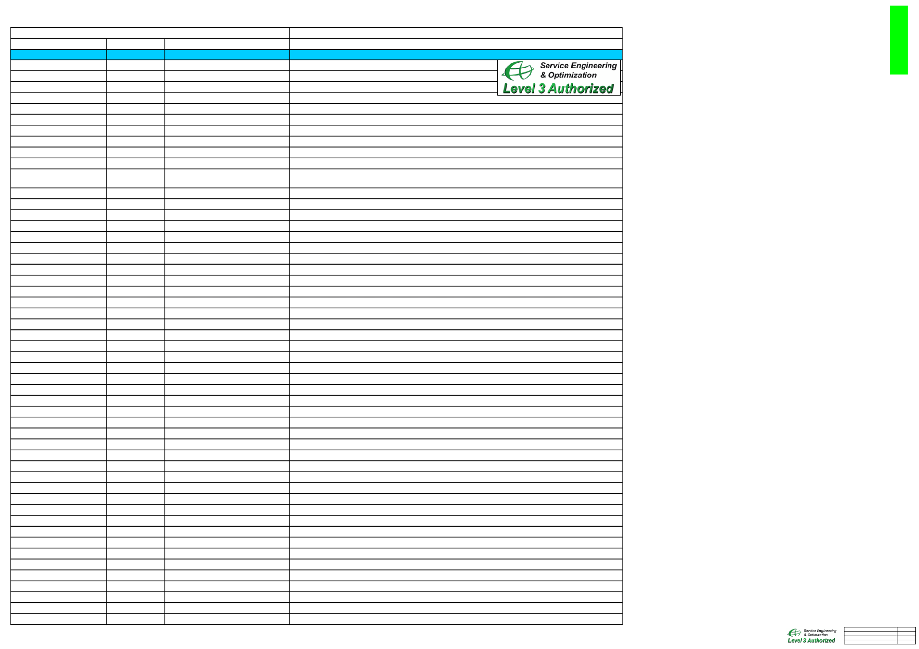
W215/W218 EU band Block Diagram Signak Description
Signal Name
From
To
Signal Description
A/D[0..15] U101
U301
Address and data bus inputs/outputs multiplexed
A[16..23] U101
U301
Address bus outputs multiplexed
AUDAMP_SD
U101
U601
Enable pin of audio amplifier
AUXI/FM_ROUT
R131/U202
U103
Headset Microphone/FM radio input (R channel)
BATTEMP
U103
R713
NTR connect of the Battery
BS1
U101
U201
PA output ( 0 : GSM ; 1: DCS )
CAM_DATA[0..7]
J901
U902
Camera Module: Camera Data Bus
CDI
U103
U101
AUDIO CODEC port interface serial data input
CDO
U101
U103
AUDIO CODEC port interface serial data output
CKEN
U103
U101
13Mhz clock Enable
CKM
U101
U301
Synchronizes the memory to the frequency of the EMIF during synchronous operations such as
burst mode.
CLK13M
U101
U103
13Mhz clock
CLK32K
U103`
U101
32Khz clock
COL[0..4]/ROW[0..4]
U101
Keypad Matrix
Forms part of Keypad Matrix
CSCLK
U101
U103
AUDIO CODEC port interface serial clock
CSYNC
U01 U103
AUDIO CODEC port interface frame synchro
CTS_MODEM
U101
TP1
Clear To Send
EARN
U103
Voice Receiver
Negative Audio Voice to Receiver
EARP
U103
Voice Receiver
Positive Audio Voice to Receiver
FDP
U101
U301
The Flashreset/deeppower-downmode control
FM_ANT
J602
C222
FM Antenna
FM_LOUT
U202
U103
FM radio input(L channel)
HB_IN
R202
U201
TX VCO generated transmit DCS Frequency
HS_BIAS
U101
U604
Enable pin of the eadset microphone bias
HS_DETECT
U101
J602
Headset Detection
HS_EN
U101
U605/U602
Analog switch control(MODEM or Headset)
HS_HOOK
U603
U101
Handset send/end key detection
HSMIC
C112
U103
Headset Microphone amplifier input (single ended)
HSOL
U103
C623
Headset 32 ohm driver (L channel)
HSOR
U103
C626
Headset 32 ohm driver (R channel)
ICTLAC1
U103
U502
Charge current control signal
KEY_BL
U101
R710
When this signal goes high, the Keypad backlights are illuminated
LB_IN
R201
U201
TX VCO generated transmit GSM Frequency
LCM_RESET
U101
LCM
LCM reset pin
LED+
U701
LCM
LCM BackLight LED driver
LEDLCM_EN
U101
U701
LCM BackLight LED Enable
MICBIAS
U103
R601
Microphone bias supply(2V)
MICIN
C607
U103
Negative analogue uplink audio from on board Microphone
MICIP
C601
U103
Positive analogue uplink audio from on board Microphone
MODE_DETECT
R618/R620
U103
EarJack function detection
nBHE
U101
U301
Enable to address High Byte Information
nBLE
U101
U301
Enable to address Low Byte Information
nFADV
U7 U10/U108
Indicates to memory device that a valid address is present on the address inputs
nFOE
U101
U301
Flash and SRAM output Enable - Active Low
nSC0
U101
U301
Used as Chip Enable for the PSRAM
nSC3
U101
U301
Used as Chip Enable for the Flash Memory
PA_EN
U101
U201
Chip enable for PowerAmp IC
PCHGAC
U103
R501
Battery Pre-charge Path
PCLK
J901
U902
Camera Module: Pixel clock output
RNW
U101
U301
Read and Write - allows information to be wriiten or read from the memory devices
RPWON S802
U101
ON button
Level3Schematics
HansonKo
2007.04.27
Rev.1.0
Page1of2
W215/W218
W
21
5
/W
21
8
RX_DCSM/RX_DCSP
BF202
U101
Received DCS Antenna Frequency Signal
RX_EGSMM/RX_EGSMP BF201
U101
Received GSM Antenna Frequency Signal
RX_MODEM U101
U607
Receive Data
SCL1
U101
U103
I2C interface Master serial clock reserved for TriTon Lite Control
SCL2
U101
U202
I2C interface Master serial clock reserved for FM Control
SCLK
U101
U902
Serial Clock Input for backend IC or LCM
SDA1
U101
U103
I2C interface Serial bi-directional data reserved for TriTon Lite Control
SDA2
U101
U202
I2C interface Serial bi-directional data reserved for FM Control
SENSOR_power_EN
U901
U902
Camera Enable
SIO_C
U902
J901
Camera Module: SCCB serial interface clock input
SIO_D
U902
J901
Camera Module: SCCB serial interface data I/O
SPI_CLK
U101
LCM
LCM serial clock
SPI_nCS
U101
LCM
LCM chip select i output
SPI_SIMO
U101
LCM
LCM serial data master-out
SPKN/SPKP
U103
U601
Speaker Audio Amp output
SW_HI_TX
U101
T201
DCS TX enable
SW_LO_TX
U101
T201
GSM TX enable
TCK
U101
TP111
CLK of JTAG
TDI
TP112
U101
Data input of JTAG
TDO
U103
TP109
Data output of JTAG
TMS
TP110
U101
JTAG mode selection
TRSTN
TP113
U101
JTAG RESET
TX_MODEM U101
U608
Transmit Data
TXHB/TXLB
U101
R201
In-phase baseband codec uplink signals
USIM_CLK
U101
J701
SIM Card Reference Clock
USIM_IO
U101
J701
SIM Card I/O Data
USIM_PWCTL
U101
J701
SIM Pull-Up power control
USIM_RST
U101
J701
SIM Card Reset
VAC
U501
U103
Power Supply of Charge system
VAPC
U101
R206
Automatic Powert Control - Sets the PA output level
V_AVDD
U901
J901
Camera Module: Camera module power supply
VBACKUP
U103`
C106
RTC battery Voltage Back up
VBAT J703
U102/U103/U201/U202/R503/U601Battery Voltage for supply purposes
VBATS
R503
U103
Charging current sense
V_BE_CORE
R907
U902
Regulator for backend IC
VCCS
R503
U103
Charging current sense
VCHG
J501
U501
Adaptor DC input
VRABB
U103
U103
Power supply of U10
VREXTH
U103
U101
For DRP
VREXTL
U103
U101
DBB core voltage
VRIO
U103
U101/U202/LCM/R623/R631
I/O of the LCM .FM,and U101
VRMEM
U103
U101/U301
For Flash power supply
VRMMC
U103
U101/R211/R213
For RF power supply
VRPLL
U103
U103
DPLL/APLL subchip dedicated power supply inside DBB
VRRTC
U103
U103
Regulator RTC output
VRSIM
U103
J701
For SIM card power supply
VRUSB
U103
TP128
USB power
VSYNC
J901
U902
Camera Module: Vertical sync output
Wait
U101
U301
Flash and synchronous PSRAM- specific signal configureable true-level output
XCLK
J901
U902
Camera Module: System clock input
Level3Schematics
HansonKo
2007.04.27
Rev.1.0
Page2of2
W215/W218
W
21
5
/W
2
18
Document Outline
Wyszukiwarka
Podobne podstrony:
W215 W218 Block Diagram
W215 W218 Signal Flow
block diagram
ALAN42MULTI block diagram
20060919095901218 09 Block Diagram
Block Diagram
System Block Diagram
ZEUS PRO BLOCK DIAGRAM
block diagram
Block Diagram
W215 W218 schematics
Block Diagram 2
POG IF Block Diagram
Thomson MT5655 BLOCK DIAGRAM
W215 W218 Layout Placement
Block Diagram W510 L3 C A3 V1 0 Block Diagrams
Block Diagram V9POIFBlDi V975 L3 2[1] 0 050131145018
Block Diagram
więcej podobnych podstron