Power Electronics Technology August 2008
www.powerelectronics.com
20
Choose Your IGBTs Correctly
for Solar Inverter Applications
By Wibawa Chou, Application Engineer,
International Rectifier, El Segundo, Calif.
G
iven the many varieties of advanced power
devices available, choosing the right power
device for an application can be a daunting
task. For solar inverter applications, it is well
known that insulated-gate bipolar transistors
(IGBTs) offer benefits compared to other types of power
devices, like high-current-carrying capability, gate control
using voltage instead of current and the ability to match the
co-pack diode with the IGBT.
A solar inverter is a power-electronic circuit that con-
verts dc voltage from a solar array panel to ac voltage that
can be used to power ac loads such as home appliances,
lighting and power tools. However, getting the most out
of such a topology requires careful analysis and the right
choice of the high-side and low-side combination of an
IGBT. It also requires more insight into how an IGBT
works. A closer examination can
show why.
IGBT Technology
An IGBT is basically a bipolar
junction transistor (BJT) with a
metal oxide semiconductor gate
structure. This allows the gate of
the IGBT to be controlled like a
MOSFET using voltage instead of
current. Being a BJT, an IGBT has
higher current-handling capabil-
ity than a MOSFET.
An IGBT is also a minority
carrier device like a BJT, mean-
ing that the speed at which the
IGBT turns off is determined
by how fast the minority carrier
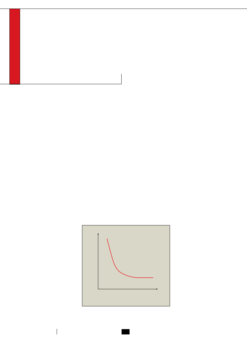
recombines. As shown in Fig. 1,
the turn-off time on an IGBT is a
tradeoff with its voltage drop (V
CEON
).
As can be seen, an ultrafast IGBT has a higher V
CEON
than a standard-speed IGBT. However, an ultrafast type
switches off much faster than a standard-speed type,
taking into consideration the same IGBT with identical
dimensions and made from the same process technology.
The tradeoff is achieved by controlling the lifetime of the
IGBT’s minority carrier recombination rate, which affects
the turn-off time.
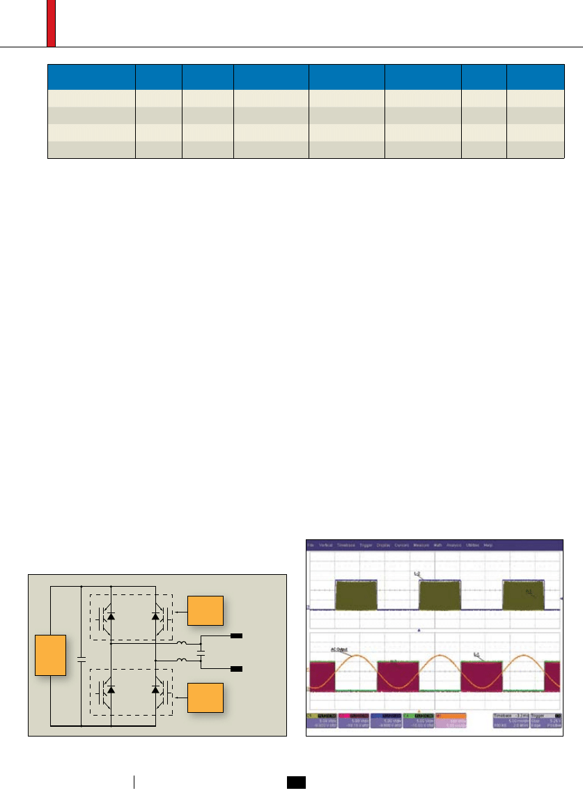
The parametric values of four IGBTs are shown in the
table. The first three are from the same planar process tech-
nology, but with different lifetime recombination control
dosage. As can be seen in the table, a standard-speed IGBT
has the lowest V
CEON
, but the slowest fall time compared to
the other two fast and ultrafast planar IGBTs. The fourth
IGBT is a trench-gate IGBT optimized to deliver low con-
duction and switching losses for
high-frequency switching such
as in solar inverter applications.
Note that the V
CEON
and total
switching loss (E
TS
) values of
the trench-gate IGBT are lower
than those of the ultrafast planar
IGBT.
A typical implementation
of a solar inverter employs a
full-bridge topology using four
switches (Fig. 2). Here, Q1 and
Q3 are designated as high-side
IGBTs while Q2 and Q4 are des-
ignated as low-side IGBTs. The
inverter is designed to produce
a single-phase ac sinusoidal volt-
age waveform at a frequency and
voltage that depend on the market
application for which the inverter
The right combination of high-side and low-side
bridge topology can ensure low power dissipa-
tion, high current carrying and gate-control
benefits of IGBTs.
Fig. 1. Turn-off time for an IGBT is a function of its
collector-emitter voltage (V
CE
). Ultrafast IGBTs have
shorter turn-off times than standard-speed IGBTs.
Figure 1
V
CE
ON
Turn-off time
Ultrafast
Standard

Power Electronics Technology August 2008
www.powerelectronics.com
22
BenefITs of IGBTs
Fig. 3. Gate-drive signals for IGBTs Q1 to Q4 in Fig. 2 and the out-
put ac sinusoidal voltage at the filter formed by L1, L2 and C1.
is intended. One such market is inverters for residential in-
stallation tied to the power grid, with net metering benefits
in some regions. This application requires the inverter to
produce a low-harmonics ac sinusoidal voltage, because
power is being injected into the grid.
One way to achieve this requirement is by pulse-width
modulating the IGBTs at or above 20 kHz at a certain
modulation frequency of 50 Hz or 60 Hz. By using pulse-
width modulation, output inductors L1 and L2 can be kept
reasonably small and will suppress the harmonics effectively.
Audible noise from the inverter also can be minimized
since the switching frequency is above the normal human
hearing spectrum.
What is the best way to pulse-width modulate these
IGBTs that will give the lowest-possible power dissipation?
One way is to only pulse-width modulate the high-side
IGBTs and to commutate the opposite low-side IGBTs at
50 Hz or 60 Hz.
Fig. 3 shows a typical gate-voltage signal. Here, Q1 em-
ploys pulse-width modulation while Q4 is kept on during
the positive half-cycle. Q2 and Q3 are kept off during this
positive half-cycle period. During the negative half-cycle,
Q3 is pulse-width modulated while Q2 is kept on. Q1 and
Q4 are kept off during this negative half-cycle. Fig. 3 also
shows the resulting ac sinusoidal voltage waveform across
output-filter capacitor C1.
This switching technique has several advantages:
l
Current does not freewheel on the high-side co-pack
diodes, minimizing unnecessary losses.
l
Low-side IGBTs only switch at a line frequency of
IGBT
Process
Speed
V
CEON
at I
C
=
20 A and 150°C
T
F
at I
C
=
20 A and 150°C
E
TS
at I
C
=
20 A and 150°C
Q
G
R
TH
IRG4PC40SPBF
Planar
Standard
1.2 V
700 ns
8.0 mJ
100 nC
0.77°C/W
IRG4PC40FDPBF
Planar
Fast
1.5 V
270 ns
4.0 mJ
100 nC
0.77°C/W
IRG4PC40UDPBF
Planar
Ultrafast
1.7 V
130 ns
1.8 mJ
100 nC
0.77°C/W
IRGP4063DPBF
Trench
Ultrafast
1.6 V
40 ns
1.2 mJ
95 nC
0.45°C/W
Fig. 2. A typical implementation of a solar inverter circuit using
a full-bridge IGBT topology.
IGBT
Q1
IGBT
Q3
IGBT
Q2
IGBT
Q4
L1
L2
Low-side
IGBTs
High-side
IGBTs
AC output
AC output
C1
Figure 2
Solar
panel
Performance characteristics of four types of IGBTs.
50 Hz or 60 Hz; conduction loss dominates these IGBTs.
l
There is no possibility of bus shoot-through because
IGBTs on the same leg never switch in a complementary
fashion.
l
Co-pack diodes across the low-side IGBTs can be
optimized to minimize losses during freewheeling and
reverse recovery.
High- and Low-Side IGBTs
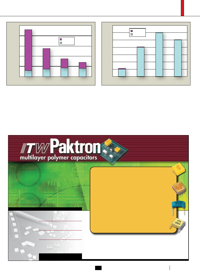
Let’s assume a 1.5-kW solar inverter is being designed
with a 230-Vac output. Which IGBT shown in the table will
give the lowest power dissipation at 20 kHz? Fig. 4 shows
the breakdown of power dissipation of the IGBTs switching
at 20 kHz as discussed earlier. One can see that the ultrafast
planar IGBT has the lowest total power dissipation com-
pared to the other two planar IGBTs.
This is obviously due to the fact that at 20 kHz, switch-
ing loss becomes a very important component to the
total power dissipation of the IGBT. As can be seen, the
standard-speed IGBT has the lowest conduction loss, but
its highest switching loss makes the device unsuitable for
the high-side IGBTs.
The latest 600-V trench IGBT is optimized for switch-
ing at 20 kHz. It can be seen that this IGBT has lower total
power dissipation compared to the previous-generation
planar IGBT (Fig. 4). We can conclude that the highest ef-
ficiency possible for a solar inverter design, a trench-gate

www.powerelectronics.com
Power Electronics Technology August 2008
23
IGBT, is the device of choice for the high-side IGBTs.
The same question arises for the low-side IGBTs. Which
IGBT is the best device that will give the lowest power
dissipation? Since these IGBTs switch at only 50 Hz or 60
Hz, a standard-speed IGBT will provide the lowest power-
dissipation level (Fig. 5).
5.0
10.0
15.0
20.0
25.0
0.0
Po
w
er dissipa
tion (
W
)
P
SWITCHING
P
CONDITION
IRG4FPC40SPBF
Standard planar
IRG4PC40FDPBF
Fast planar
IRG4PC40UDPBF
Ultrafast planar
IRGP4063DPBF
Ultrafast trench
20.0 W
3.8 W
3.0 W
10.0 W
4.5 W
4.3 W
3.0 W
4.0 W
Figure 4
Fig. 4. Ultrafast IGBTs switching at 20 kHz provide the lowest
power-dissipation levels compared to fast and standard-speed
devices. And of the two ultrafast types shown on the right, a
trench-gate IGBT dissipates the least amount of power.
Figure 5
IRG4FPC40SPBF
Standard planar
IRG4PC40FDPBF
Fast planar
IRG4PC40UDPBF
Ultrafast planar
IRGP4063DPBF
Ultrafast trench
Po
w
er dissipa
tion (
W
)
5.5
6.0
7.0
8.0
9.0
6.5
7.5
8.5
0.060 W
0.030 W
0.014 W
0.009 W
6.0 W
7.5 W
8.5 W
8.0 W
P
SWITCHING
P
CONDITION
Fig. 5. Switching at 60 Hz, the lowest level of power dissipation
from a low-side IGBT is achieved using standard-speed IGBTs.
Although a standard-speed IGBT shows some switching
loss, the loss value is so insignificant that the total power
dissipation of this IGBT is not affected by its switching loss
component. In fact, the latest trench-gate IGBT still features
higher power dissipation, because this generation is targeted
at high-frequency applications with balanced switching and
conduction losses. Thus, for low-side IGBTs, a standard-
speed planar IGBT is still the device of choice.
PETech
BenefITs of IGBTs
■
MADE IN USA
■
LONG-LIFE
■
HIGH RELIABILITY
Mission
1205 McConville Road
■
Lynchburg, Virginia 24502
tel. 434.239.6941
■
fax. 434.239.4730
Applications
Critical
MULTILAYER POLYMER (MLP) CAPACITORS
■
Ultra low ESR and ESL
■
High Ripple Current Handling
■
Stable Under AC & DC Voltage
■
Military/Telecom/Datacom 99.999% (5x9) Up Time
■
Low Profile For Surface Mount
■
Robust Mechanical and Electrical Design
■
50 to 500 Volts
APPLICATIONS
■
48 Volt Telecom/Datacom
■
HEV - Hybrid Electric Vehicle Boost Converters
■
High Voltage Bus from 48 to 440+ Volts
■
PFC Front Ends & SMPS Off-Line
■
RFI/EMI Suppression
www.paktron.com
AVAILABLE THROUGH THESE DISTRIBUTORS:
Atlantic Components (1-800-433-6600)
Cornell Dubilier/Mallory (1-508-996-8561)
Future (1-800-388-8731)
Gopher (1-800-592-9519)
www.paktron.com
Wyszukiwarka
Podobne podstrony:
Microprocessor Control System for PWM IGBT Inverter Feeding Three Phase Induction Motor
An Optically Isolated Hv Igbt Based Mega Watt Cascade Inverter Building Block For Der Applications
How an inverter fits into your solar electric system By Jo
Microprocessor Control System for PWM IGBT Inverter Feeding Three Phase Induction Motor(1)
Inverter Pilota Isolato Igbt(2)
An Igbt Inverter For Interfacing Small Scale Wind Generators To Single Phase Distributed Power Gener
Microprocessor Control System for PWM IGBT Inverter Feeding Three Phase Induction Motor(1)
3 Phase inverter IGBT SEMITOP3 module
Microprocessor Control System for PWM IGBT Inverter Feeding Three Phase Induction Motor
An 9021 A Novel Igbt Inverter Module For Low Power Drive Applications
Solar
[ebook renewable energy] Home Power Magazine 'Correct Solar Panel Tilt Angle to Sun'
Igbt model spice
artyki IGBT
HF 91110 80 Amp Inverter Arc Welder
an889a inverter
więcej podobnych podstron