
Journal of Crystal Growth 260 (2004) 54–62
Resistivity control in unintentionally doped GaN films grown
by MOCVD
A.E. Wickenden*, D.D. Koleske
1
, R.L. Henry, M.E. Twigg, M. Fatemi
Electronics Science and Technology Division, Code 6800, Naval Research Laboratory, Washington, DC 20375-5320, USA
Received 28 April 2003; accepted 19 August 2003
Communicated by C.R. Abernathy
Abstract
The relationship of GaN resistivity to film microstructure and impurity compensation are investigated using
transmission electron microscopy, secondary ion mass spectroscopy, X-ray diffraction, and resistance measurements.
Unintentionally doped GaN films grown by MOCVD at varying pressures exhibit increased grain size, reduced carbon
and oxygen impurity incorporation, reduction in the density of threading dislocations (TDs) with an edge component,
and reduced resistivity with increasing growth pressure. Variation in resistivity over eight orders of magnitude is
observed as a result of varying the MOCVD growth pressure in a controlled experiment. Our results suggest that
disclocations play an important role in the resistivity of GaN. Evidence is presented of impurities segregating at TDs
having an edge component, and acting as compensating centers. The control of such compensation as a function of
MOCVD growth conditions is outlined.
Published by Elsevier B.V.
Keywords: A1. Compensation; A1. Impurities; A1. Threading dislocations; A3. Metalorganic vapor phase epitaxy; B2. Semicon-
ducting gallium nitride
1. Introduction
The III-nitride system is attractive for high-
power microwave applications due to the large
breakdown voltage of the wide band gap materi-
als, as well as their ability to realize high sheet
carrier densities in the two-dimensional electron
gas (2DEG) region formed at the AlGaN/GaN
interface. Highly resistive (HR) GaN is required to
facilitate device pinch-off and high frequency
operation. A large n
sheet
m product is required for
power applications, which further mandates high
electron mobility in the GaN film. We believe that
resistivity in heteroepitaxial GaN thin films, as in
many other III–V compounds, generally results
from compensation effects of deep level traps
rather than from the intrinsic wide band gap
nature of the material (e.g.
). Effects such as
persistent photoconductivity
and current col-
lapse
have been observed in GaN field effect
ARTICLE IN PRESS
*Corresponding author. Currently with US Army Research
Laboratory, AMSRL-SE-RL, 2800 Powder Mill Road, Adel-
phi, MD 20783-1197, USA. Tel.: +1-301-394-0094; fax: +1-
301-394-4562.
E-mail address:
awickenden@arl.army.mil
(A.E. Wickenden).
1
Currently with Sandia National Laboratory, Albuquerque,
NM 87185.
0022-0248/$ - see front matter Published by Elsevier B.V.
doi:10.1016/j.jcrysgro.2003.08.024

transistor (FET) and AlGaN/GaN high electron
mobility transistor (HEMT) devices having under-
lying HR GaN layers. Such effects degrade device
performance, and have been associated with
trapping centers in the HR GaN
. Evidence of
deep level centers have also been observed in HR
GaN UV detector structures
. The most desir-
able solution at present for optimized GaN growth
of device structures is to reduce background
donors and compensating acceptors to a mini-
mum, compensated level to achieve high resistivity
for device pinchoff, and low scatter in active device
regions for high mobility.
It is well known that heteroepitaxial growth of
GaN thin films on sapphire initiates as an
assemblage of crystallites, or grains, that coalesce
into a two-dimensional film
. These GaN films
have typical dislocation densities of 10
8
–10
10
cm
2
,
and the size and relative misorientation of the
grains are determined in part by the crystal growth
process parameters. GaN films and bulk crystals
are also known to contain relatively high levels of
background impurities
and point defects such
as vacancies
. In this investigation, we report on
the modification of GaN film resistivity through
microstructural and impurity control. Manipula-
tion of the growth conditions to tune the
concentration of defects which contribute to
GaN resistivity, and which also serve as scattering,
trapping and compensating centers in the con-
ducting regions of GaN films, has been observed
to result in significant improvements in device
performance. HEMT devices with 300 K sheet
carrier density of 1.3 10
13
cm
2
, mobility of
1500 cm
2
/Vs, and excellent pinchoff characteristics
have been demonstrated on such material.
2. Experimental procedure
2.1. Epitaxial growth
The microstructure of a heteroepitaxial GaN
film may be influenced in a number of ways,
including manipulation of the low temperature
nucleation layer (NL)
, the growth rate of
the epitaxial GaN film
, and the growth
pressure of the high temperature GaN film
For the results reported here, a series of unin-
tentionally doped (UID) GaN films was grown
using the metalorganic chemical vapor deposition
(MOCVD) technique, with growth pressure varied
from 40 to 500 Torr as the experimental control
variable. Each film was grown in a single-wafer
close spaced showerhead reactor, on a-plane
ð1 1 %2 0Þ sapphire substrates. An AlN NL of
approximately 250 (
A thickness was grown under
identical conditions for each film. The NL was
deposited at a temperature of approximately
700
C, at a chamber pressure of 40 Torr, using
1.23 mmol/min trimethylaluminum (TMA) and
0.089 mol/min ammonia (NH
3
) in a hydrogen
(H
2
) ambient. The GaN epilayer growth condi-
tions were held constant, using a growth tempera-
ture of approximately 1035
C, input reactant
fluxes of 21.5 mmol/min trimethylgallium (TMG)
and 0.071 mol/min NH
3
, in a H
2
ambient. Total
flows for both the NL and GaN epilayer were held
at 4 slm, and the MOCVD chamber pressure was
adjusted by varying the throttle valve setting on
the chamber exhaust. Growth pressure was ad-
justed immediately after NL growth, hence the
AlN NL was ramped up to the GaN growth
temperature at the pressure at which the GaN film
was subsequently grown. Seven UID-GaN films
were grown at pressures of 40, 65, 110, 130, 150,
300, and 500 Torr, respectively. A reduction in
GaN growth rate with increasing growth pressure
has been previously observed due either to the
decomposition of GaN in H
2
to form NH
3
,
or gas phase depletion of reactants
. The GaN
growth rate in this experiment varied nominally in
the range of 0.5–1.5 mm/h, with the lowest growth
rate observed at the highest growth pressure. In an
effort to maintain constant film thickness within
this experimental set, the time of each growth was
adjusted to yield a film thickness of approximately
1 mm. To independently investigate the contribu-
tions of microstructure and unintentional impurity
incorporation to the carrier compensation of the
GaN films, two additional films were grown. In the
first of these, the microstructure having approxi-
mately 0.5 mm grain size was established by the
initial growth of a 0.5 mm thick layer of GaN at a
pressure of 130 Torr. The growth was then stopped
for 2 minutes during which the chamber pressure
ARTICLE IN PRESS
A.E. Wickenden et al. / Journal of Crystal Growth 260 (2004) 54–62
55
was adjusted to 300 Torr, and an additional 1.5 mm
thickness of GaN was grown. In the second film,
the microstructure having approximately 2 mm
grain size was established by the initial growth of
a 0.5 mm thick layer of GaN at a pressure of
500 Torr. After stopping growth, the chamber
pressure was adjusted to 130 Torr, and an addi-
tional 1.5 mm thickness of GaN was grown. In the
following discussion, these bilayer films will be
referred to as 130/300 and 500/130, respectively, to
indicate the first film growth condition followed by
the subsequent film growth condition.
2.2. Characterization
The resistance of the UID GaN films was
measured by I =V characterization of squares
patterned on each sample, using large indium
stripe contacts to reduce measurement error
associated with contact resistance. Values of
resistivity, r; were derived using the relationship
r ¼ RA=L; where R is the resistance calculated
from the I =V measurements, A is the cross-
sectional area of the GaN film (1 mm GaN film
thickness 0.5 cm indium stripe length), and L is
the distance between contacts on the film surface
(approximately 0.3 cm). The experimental limit of
the resistivity measurement equipment was 10
10
O-
cm. Each of the films was measured at ambient
temperature, in the dark and with room light
illumination. The microstructure of the films was
investigated using transmission electron micro-
scopy (TEM) and X-ray diffraction analyses.
Cross-section TEM analysis was used to investi-
gate the grain size of the films, and plan-view TEM
imaging was used to measure dislocation densities.
X-ray diffraction analysis was performed in both
the symmetric {0 0 0 2} and asymmetric f1 0 %1 2g
modes, to investigate the contribution of edge,
screw and mixed-character threading dislocations
(TDs) in the films. Intrinsic impurity levels were
investigated in selected films with secondary ion
mass spectroscopy (SIMS)
. The films were
analyzed in a single SIMS experiment to ensure
equivalent background levels, and the SIMS
chamber was evacuated for >24 hours prior to
analysis to reduce the background of atmospheric
contamination in the SIMS chamber.
3. Results
3.1. GaN morphology
All of the GaN films in this study were
continuous and specular over the 2 inch wafer
diameter. Cross-sectional TEM images of the 130
and 500 Torr single pressure films, and the 130/300
and 500/130 two-pressure films, are shown in
. The images clearly demonstrate increased
ARTICLE IN PRESS
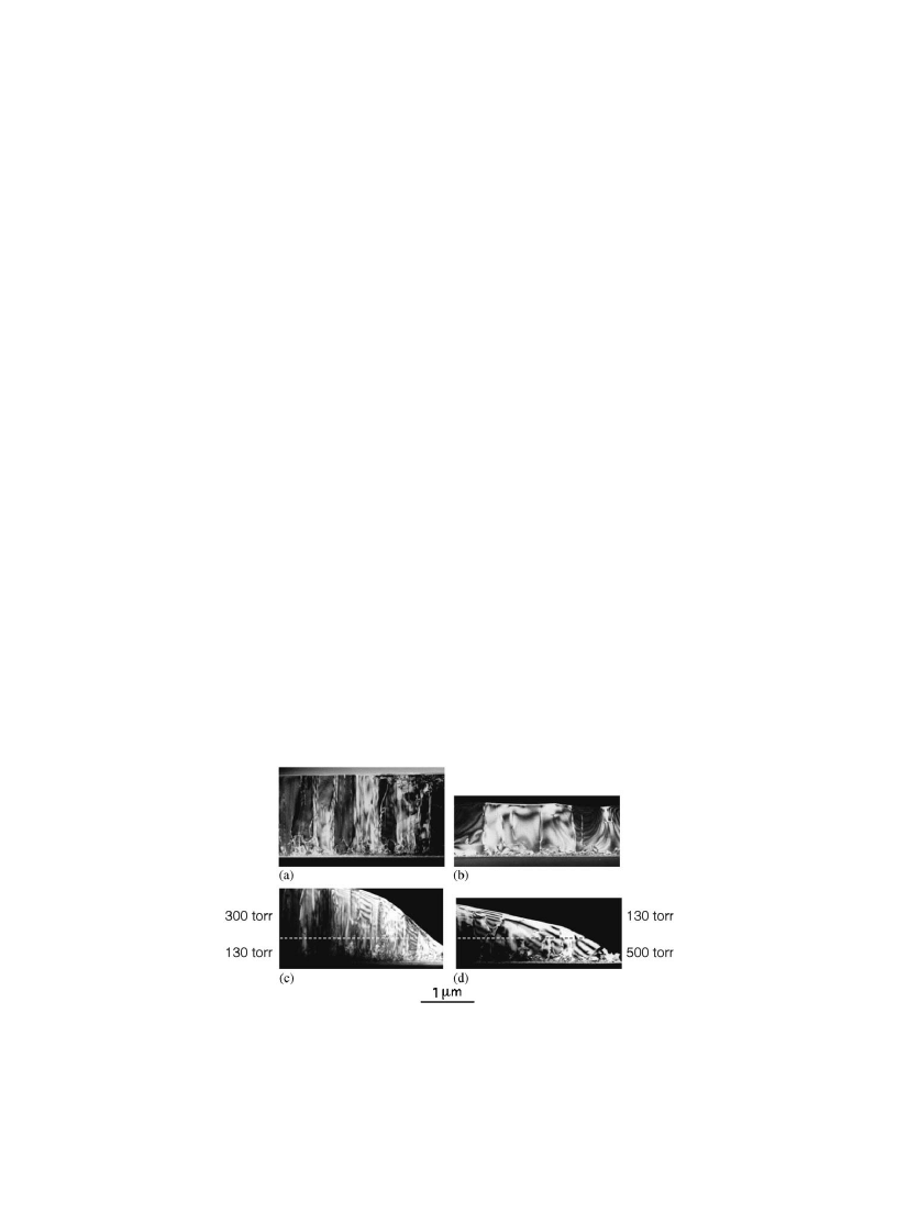
Fig. 1. Cross-sectional TEM images of UID-GaN films, grown at pressures of: (a) 130 Torr, (b) 500 Torr, (c) 130/300 Torr, and (d)
500/130 Torr. The grain size is determined from the change in diffraction contrast due to slight misorientation of adjacent grains. The
grain size of films (b) and (d), established at the higher pressure, is approximately 2 mm, and the total dislocation density measured
using plan-view TEM analysis is 1 10
9
cm
2
. The grain size of films (a) and (c), established at the lower pressure, is approximately
0.5 mm, and the dislocation densities from plan-view TEM analysis are 4 10
9
cm
2
for both (a) and (c).
A.E. Wickenden et al. / Journal of Crystal Growth 260 (2004) 54–62
56
grain size with increasing growth pressure (
), a trend observed in previous studies
Further inspection of the two-pressure films
illustrates that the microstructure of an overgrown
GaN layer is determined by that of the initial
growth (
). Plan-view TEM analysis
revealed a total (edge, screw, and mixed) TD
density of 4 10
9
cm
2
in the 130 Torr and 130/
300 Torr films, 2 10
9
cm
2
in the 300 Torr film,
and 1 10
9
cm
2
in the 500 Torr and 500/130 Torr
films. The plan-view TEM images showed correla-
tion between TDs and the grain boundaries
observed in
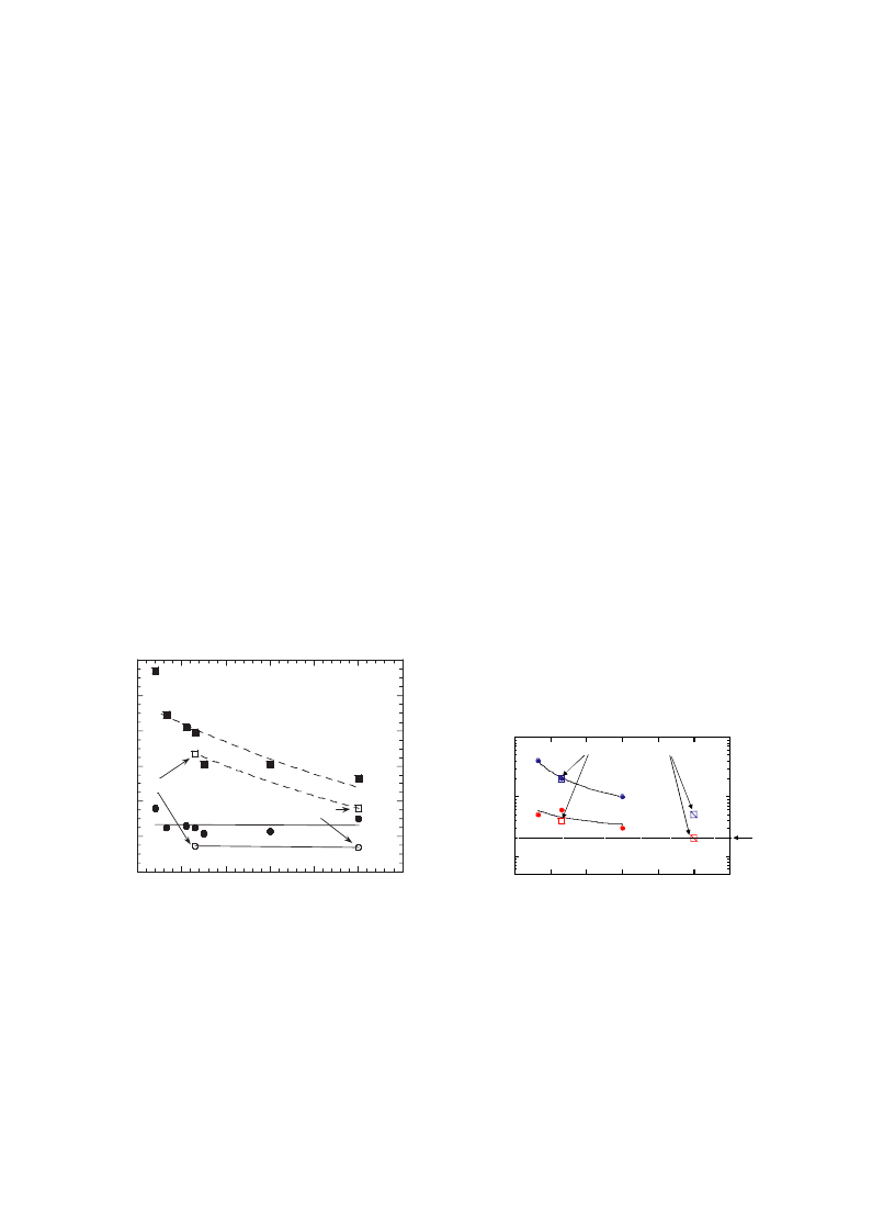
. X-ray diffraction data for the
films is shown in
. The general reduction of
FWHM values in the two-pressure films is
attributed to the fact that they are twice as thick
as the single-pressure films in the study. The X-ray
data for the thicker films is less subject to peak
broadening due to small sample volume, and less
influenced by the highly defective GaN interface
with the NL. The FWHM of the {0 0 0 2}
symmetric reflection, which is sensitive to screw-
type TDs
, appears to be insensitive to growth
pressure over a fairly broad pressure range. The
off-axis f1 0 %1 2g data, which is sensitive to screw
plus edge and mixed-character TDs, shows a
definite decreasing trend as a function of increas-
ing growth pressure. It is further observed from
the off-axis data that the two-pressure films appear
to follow the trend of the single-pressure films that
form the initial film growth. The X-ray diffraction
data is consistent with the plan-view TEM analysis
of TD density, and suggests that the ratio of edge-
type and mixed-character TDs to screw-type TDs
is decreasing with increasing growth pressure over
most of the pressure range investigated. Since
edge-type TDs are known to form at grain
boundaries to accommodate slight misorientation
between the grains
, the X-ray data is also
consistent with the increasing grain size observed
in the films grown with increasing growth pressure.
3.2. Background impurity analysis
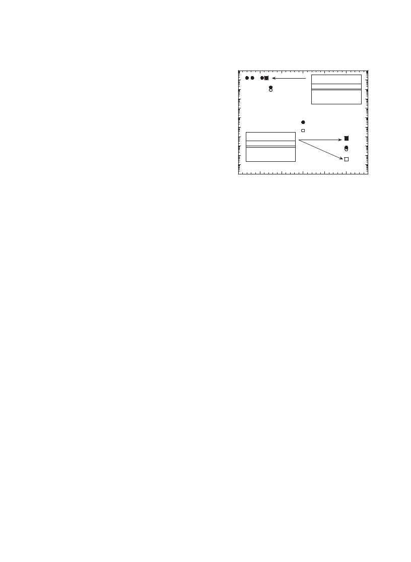
SIMS data demonstrates an order of magnitude
decrease in the UID carbon concentration with
increasing growth pressure, from 4 10
17
cm
3
at
65 Torr to 5 10
16
cm
3
in the 500/130 Torr film,
as illustrated in
. The concentration of UID
oxygen decreases with increasing pressure by less
than a factor of three over the same pressure
ARTICLE IN PRESS
200
400
600
800
X-ray FWHM (arc-sec)
1000
1200
1400
0
100
200
300
400
500
600
Growth Pressure (torr)
500/130 torr
130/300 torr
Fig. 2. X-ray diffraction data for the GaN films in this study,
plotted as a function of growth pressure. Circles represent data
for the /0 0 0 2S reflection (sensitive to screw-type TDs), and
squares represent data for the 1 0 %1 2
reflection (sensitive to
total dislocations, including edge and mixed-character TDs).
Closed symbols represent data for single pressure GaN films,
and open symbols are data for two-pressure films, which are
plotted relative to the pressure of the underlying film since the
TEM data shows that the microstructure was fixed by the initial
film growth. The lines through data points are provided as a
guide to the eye.
10
16
10
concentration (cm
-3
)
17
10
18
0
100
200
300
400
500
600
GaN growth pressure (torr)
SIMS
detection
limit for C, O
130/300 torr film
500/130 torr film
Closed circles:
single pressure
films
Open squares:
Two-pressure films
carbon
oxygen
Fig. 3. SIMS analysis of carbon and oxygen for UID-GaN
films grown at MOCVD pressures of 65, 130, and 300 Torr
(closed circles), demonstrates the trend of reduced carbon and
carbon:oxygen ratio with increasing pressure. SIMS data for
the 130/300 Torr and 500/130 Torr UID-GaN films (open
squares) is plotted relative to the pressure of the underlying
film since the TEM data shows that the microstructure was
fixed by the initial growth. This plot demonstrates that the
impurity incorporation for this pressure range is associated with
TDs in the films. The lines through data points are provided as
a guide to the eye.
A.E. Wickenden et al. / Journal of Crystal Growth 260 (2004) 54–62
57
range, decreasing from 5 10
16
to 2 10
16
cm
3
.
Unexpectedly, carbon and oxygen levels were
constant through the depth of the two-pressure
films, at levels that corresponded to those expected
for the pressure used to grow the initial portion of
the films. The significance of the impurity profiles
of the two-pressure films will be discussed below.
The concentration of silicon, a donor impurity,
was not measured in these films, but SIMS analysis
of GaN films grown in this reactor under similar
process conditions have repeatedly demonstrated
UID silicon impurity concentrations below the
SIMS detection limit of 2 10
16
cm
3
. Simi-
larly, the concentrations of the acceptor impurities
magnesium and zinc were not measured, since the
precursors for these impurities are not used in this
MOCVD reactor, and previous analyses of films
grown in this reactor have shown the concentra-
tions of these impurities to be below the SIMS
detection limit.
3.3. Resistivity analysis
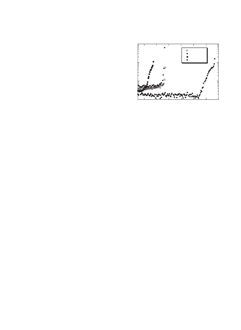
The resistivity of the single pressure UID-GaN
films is observed to decrease with increasing
growth pressure, varying over more than eight
orders of magnitude as illustrated in
. The
films in this series grown at pressures
p130 Torr
reached the experimental limit of measurable
resistance. The resistivity of films grown at
pressures >130 Torr decreases monotonically with
pressure, indicating an exponential relationship.
The measured resistivities of the 130/300 and 500/
130 Torr films are plotted relative to the growth
pressure of the underlying portion of these films,
which presents the most reasonable fit to data for
the single-pressure films. The significance of this
correlation will be discussed below. The difference
in light and dark resistivity measurements is
observed to become much more pronounced in
the films grown at higher pressures. The difference
in light and dark measured resistivity has been
associated with trapping states that are detrimen-
tal
to
device
performance
for
AlGaN/GaN
HEMTs. The discussion of this phenomenon is
beyond the scope of the current work, but is the
subject of ongoing investigation
4. Discussion
Carbon has been demonstrated to act as an
acceptor-type electron trapping center in GaN
, and substitutional oxygen impurities have
been predicted to act as donors
. Carbon and
oxygen are considered to be the primary back-
ground impurity acceptor and donor, respectively,
in the films in this study because of the low
concentrations of silicon donors and the absence
of zinc and magnesium acceptors in the growth
chamber. TDs have also been associated with
charge centers in GaN films, and must be
considered in the discussion of compensation
mechanisms governing the resistivity of UID
GaN films. Elsner and co-workers have modeled
both the open-core screw TD and the edge TD as
electrically inactive
, but predicted that the
stress fields surrounding the edge-type TD could
trap gallium vacancies, oxygen, and V
Ga
–O com-
plexes. These authors further suggest that the
Ga-vacancy and oxygen-related complexes act as
deep acceptors, with energy levels in the range of
0.3–0.8 eV above the valence band maximum
.
ARTICLE IN PRESS
10
0
10
2
10
4
10
6
10
8
10
resistivity (ohm-cm)
10
0
100
200
300
400
500
600
growth pressure (torr)
500/130 torr GaN
130/300 torr GaN
~1.5 µm GaN @ 300 torr
sapphire
~0.5 µm GaN @ 130
t
~2.0 µm GaN @ 130
sapphire
~0.5 µm GaN @ 500
t
Fig. 4. Resistivity of UID-GaN films as a function of epitaxial
growth pressure measured in the dark (closed symbols) and in
ambient room light (open symbols). The values were derived
from I=V characterization using indium stripe contacts on
squares patterned in the GaN films (see text). The experimental
limit of the resistivity analysis is reached at a level of 10
10
O-cm.
Data for the two-pressure films is again plotted relative to the
pressure of the underlying film. Inserts for the two-pressure
films illustrate the respective film structures.
A.E. Wickenden et al. / Journal of Crystal Growth 260 (2004) 54–62
58

Northrup has predicted the formation of Ga-filled-
core screw TDs under Ga-rich conditions, having
energy levels throughout the band gap and thus
being metallic, and predicted to serve as conduc-
tive pathways through the GaN film
. Recent
work by Krtschil and co-workers has suggested
decoration of TDs with impurities, contributing to
a charge on the dislocation core
.
Given substitutional incorporation of carbon
and oxygen on the GaN lattice, it may be
reasonable to assume that the reduction in the
C:O ratio observed with increasing growth pres-
sure (
) is related to reduced compensation in
the films in this study. In the case of the GaN film
grown at 40 Torr, impurity compensation and
scatter from crystalline disorder as evidenced by
high levels of both screw- and edge-type TDs
are also consistent with the measured high
resistivity. In separate multiple-pressure experi-
ments, we have observed carbon incorporation to
increase dramatically with decreasing growth
pressure for GaN films grown at pressures
o100 Torr, with carbon incorporation varying
over an order of magnitude in films where growth
rate varied by only 10%. In those experiments,
GaN films which were grown at very low pressures
(40–65 Torr) on films which had been grown at
higher pressures (130–300 Torr) exhibited sharp
distinctions in carbon impurity incorporation
corresponding to the interfaces between the GaN
films grown at the different pressures
. In the
present study, the two-pressure films were grown
using pressures >100 Torr, and no such distinc-
tions were observed in the SIMS data for either
sample. It is significant that the concentrations of
carbon and oxygen observed in
for the 130/
300 and 500/130 Torr films correspond to impurity
concentrations expected for the initial segment of
the GaN film growth (i.e., 130 and 500 Torr,
respectively) throughout the depth of the films,
rather than reflecting the levels for the respective
growth pressures of the single-pressure films. It is
also significant that the measured resistivity of the
two-pressure films corresponds to that of the
initial GaN growth that establishes the micro-
structure of the full film, rather than to that of the
film where the lower carbon level was anticipated
from the single-pressure film data. This unantici-
pated result demonstrates that compensation
effects are not related simply to a uniform
distribution of impurities in the bulk thin film as
a function of specific growth conditions, but that
under certain growth conditions may actually be
dominated by impurities that segregate on or near
TDs. The concentrations of TDs with an edge
component and carbon and oxygen impurities are
all observed to decrease as a function of increasing
growth pressure in this study. The carbon con-
centration varies exponentially with pressure for
growth pressures >100 Torr, and is higher than
expected from extrapolation of the plot in
for pressures
o100 Torr. This result is consistent
with the mechanism of carbon removal as a
function of hydrogen pressure
being dominant
except for carbon incorporation at sites near
dislocations with an edge component. The results
observed for the two-pressure films indicate that
for GaN films grown at MOCVD pressures
>100 Torr, the incorporation of C and O impu-
rities is dominated by the microstructure of the
GaN rather than by other kinetic growth mechan-
isms. A reduction of acceptor-type centers by
control of microstructure would be expected to
yield reduced compensation and thus decreasing
resistivity, consistent with the observed data of
. Our data would suggest that carbon
segregates at or near edge-type TDs in UID
GaN, and acts as a compensating acceptor. Our
data further suggests that carbon may incorporate
both in the lattice and near TDs with an edge
component in the pressure regime
o100 Torr, but
incorporates primarily near TDs with an edge
component for growth pressure >100 Torr.
The possibility of screw-type TDs having Ga-
filled cores as proposed by Northrup
, or
otherwise acting as sources of leakage current
must also be analyzed as a source of charge
reducing the resistivity of the UID GaN films. This
mechanism does not appear to be dominant in the
present study. The resistivity of the single-pressure
GaN films is observed to decrease dramatically
with increasing growth pressure, with almost no
variation in screw-type TD density over the range
of growth pressure investigated. Northrup’s model
suggests a crossover in the growth process where
Ga-filled-core screw-type TDs are energetically
ARTICLE IN PRESS
A.E. Wickenden et al. / Journal of Crystal Growth 260 (2004) 54–62
59
favored over open-core screw-type TDs as the
growth conditions become more Ga-rich. The
possibility of a change in character of the screw-
type TDs from open-core to Ga-filled core as
growth conditions are modified to yield a more
Ga-rich growth condition must be considered. In
earlier work
, we have demonstrated that for
pressures >100 Torr,
GaN decomposition
is
enhanced with increasing pressure, with nitrogen
removed from the GaN surface as NH
3
and
atomic or liquid Ga left behind. In both of the
two-pressure films in the present study, however,
the measured properties of the GaN films appear
to be related to the microstructure of the under-
lying GaN film, even though the local growth
environment of the film in direct contact with the
electrical probes had changed significantly. These
results are consistent with our analysis that the
TDs with an edge component, rather than
conductive screw dislocations, are the dominant
structural feature responsible for the resistivity
variation seen in the films.
Several groups have reported the presence of a
buried conductive layer (BCL) near the sapphire
substrate interface
. In all cases, the GaN
films under investigation were n-type conductive,
rather than resistive as are the films of the present
study. C=V analysis of the films in this study
observed evidence of a BCL in the film grown at
500 Torr, with an indicated electron concentration
of approximately 1 10
16
cm
3
at the interface,
which was determined to be near the detection
limit of the C=V analysis
and is close to the
UID concentration of oxygen in the film. No
evidence of BCL was observed in the 500/130 Torr
film or any of the other films grown at lower
pressures. The reduced data of
is the value
of the flat region of each SIMS profile, in the bulk
of the GaN thin film. A variation in the character
of the oxygen profiles near the sapphire substrate
interface is observed as a function of GaN growth
pressure, as illustrated in
. In lower pressure
growths (65 and 130 Torr), the oxygen concentra-
tion profile is flat with a sharp increase at the
substrate interface, but an oxygen shoulder is seen
in the data for the films where growth is initiated
at higher pressures (300 and 500 Torr). Under
higher pressure growth conditions, the GaN
growth rate is reduced and the coalescence time
is increased, possibly enhancing oxygen diffusion
from the sapphire substrate into the GaN film
until the film is fully coalesced. Upon coalescence
of the GaN film, however, an oxygen level due to
background impurities within the reaction cham-
ber is reached, which is the level plotted in
.
Oxygen impurities may be one of several sources
of interfacial conduction, but the presence of an
oxygen shoulder in the 300 Torr film, with no
observation of a BCL in the C=V analysis,
suggests that it may not be a dominant source of
conduction.
If a BCL is present, the resistance of the films
can be modeled with a simple parallel resistance
model, with the measured resistance, RðtotalÞ; is
given by
RðtotalÞ ¼ ½1=R
GaN; lateral
þ½1=ð2R
GaN; vertical
þ R
BCL
Þ
1
where R
GaN;lateral
is the resistance between the
indium contacts, R
GaN;vertical
is the resistance
through the GaN film between the indium contact
and the BCL, and R
BCL
is the resistance of the
ARTICLE IN PRESS
10
16
10
17
10
18
10
19
atomic concentration (cm
-3
)
1.0
0.80
1.2
1.4
1.6
1.8
2.0
O(65)
O( 130)
O( 300)
O(500 /1 30)
depth (micrometers)
Fig. 5. SIMS depth profiles of oxygen for four films in this
study, grown at pressures of 65 Torr (open circles), 130 Torr
(closed circles), 300 Torr (squares), and 500/130 Torr (dia-
monds). Note that the films grown at pressures of 130 Torr or
less show a sharp change in oxygen content at the GaN/
sapphire interface. In contrast, the films where growth was
initiated at 300 or 500 Torr exhibit an oxygen shoulder at the
interface, resulting in a nominally 200 nm thick layer with an
oxygen level between 2 10
16
and 8 10
17
cm
3
.
A.E. Wickenden et al. / Journal of Crystal Growth 260 (2004) 54–62
60

BCL. If we assume from the data of
a BCL
thickness of 2000 (
A, m
BCL
¼ 100 cm
2
/Vs, and an
electron concentration of 1.5 10
17
cm
3
, we
derive a reasonable value for r
BCL
¼ 0:42 O-cm.
If a constant BCL resistance is assumed to be
present for all the layers, the experimental results
of
can be fit only by allowing the resistivity
of the GaN film to vary from >10
10
O-cm at low
pressures to 10
3
O-cm at 500 Torr, still indicating a
broad range in compensation of the GaN films. If
oxygen impurities are indeed contributing to
interfacial conduction, a BCL should be present
only in the films grown at pressures >130 Torr in
this study. The observation of a BCL only in the
500 Torr film, with no BCL observed in the 500/
130 Torr film is significant. It suggests that the
BCL, if present, may not contribute significantly
to film conduction.
5. Conclusions
In this paper, we demonstrate that the resistivity
of UID GaN films may be controlled over more
than eight orders of magnitude by varying the
MOCVD growth pressure of the GaN film in a H
2
ambient. We show that with increasing growth
pressure, the GaN films exhibit increasing grain
size, decreasing density of TDs with an edge
component, decreasing carbon and oxygen con-
tent, and decreasing resistivity. The contribution
of a BCL to the measured total resistance is
analyzed and found to be too small to account for
the experimentally observed variations in resistiv-
ity. Our data demonstrates that TDs with an edge
component play a major role in the compensation
mechanisms of GaN, with carbon impurity segre-
gation at or near TDs with an edge component
resulting in compensating acceptor states. Carbon
acceptors are shown to incorporate both in the
lattice and near TDs with an edge component in
the pressure regime
o100 Torr, but incorporate
primarily near TDs with an edge component for
growth pressure >100 Torr. Substitutionally in-
corporated donors in the GaN lattice may
dominate carbon acceptors segregating at TDs
with an edge component as the concentration
of these TDs decreases, resulting in increased
conductivity consistent with the observed experi-
mental results.
Acknowledgements
The authors would like to thank L.T. Ardis for
expert TEM sample preparation and S.C. Binari
for C=V and I =V measurements. This work was
supported by the Office of Naval Research.
References
[1] R.N. Thomas, S. McGuigan, G.W. Eldridge, D.L. Barrett,
Proc. IEEE 76 (1988) 778.
[2] G. Beadie, W.S. Rabinovich, A.E. Wickenden, D.D.
Koleske, S.C. Binari, J.A. Freitas Jr., Appl. Phys. Lett.
71 (1997) 1092.
[3] S.C. Binari, K. Ikossi, J.A. Roussos, W. Kruppa, D. Park,
H.B. Dietrich, D.D. Koleske, A.E. Wickenden, R.L.
Henry, IEEE Trans. Electron. Dev. 48 (2001) 465.
[4] P.B. Klein, S.C. Binari, J.A. Freitas Jr., A.E. Wickenden,
J. Appl. Phys. 88 (2000) 2843.
[5] Z.C. Huang, J.C. Chen, D.K. Wickenden, J. Crystal
Growth 170 (1997) 362.
[6] K. Hiramatsu, S. Itoh, H. Amano, I. Akasaki, N. Kuwano,
T. Shiraishi, K. Oki, J. Crystal Growth 115 (1991) 628.
[7] I. Akasaki, H. Amano, Y. Koide, K. Hiramatsu, H.
Sawaki, J. Crystal Growth 98 (1989) 209.
[8] D.D. Koleske, A.E. Wickenden, R.L. Henry, M.E. Twigg,
J. Crystal Growth 242 (2002) 55.
[9] K. Saarinen, P. Seppala, J. Oila, P. Hautojarvi, C. Corbel,
Appl. Phys. Lett. 73 (1998) 3253.
[10] M.E. Twigg, D.D. Koleske, A.E. Wickenden, R.L. Henry,
M. Fatemi, J.C. Culbertson, Structural defects in nitride
heteroepitaxy, in: O. Manasreh (Ed.), III–V Nitride
Semiconductors: Electrical, Structural and Defect Proper-
ties, Gordon and Breach, London, 2000 (Chapter 15).
[11] D.D. Koleske, R.L. Henry, M.E. Twigg, J.C. Culbertson,
S.C. Binari, A.E. Wickenden, M. Fatemi, Appl. Phys. Lett.
80 (2002) 4372.
[12] A.E. Wickenden, D.D. Koleske, R.L. Henry, R.J. Gor-
man, M.E. Twigg, M. Fatemi, J.A. Freitas Jr., W.J.
Moore, J. Electron. Mater. 29 (2000) 21.
[13] D.D. Koleske, A.E. Wickenden, R.L. Henry, M.E. Twigg,
J.C. Culbertson, R.J. Gorman, Appl. Phys. Lett. 73 (1998)
2018;
D.D. Koleske, A.E. Wickenden, R.L. Henry, M.E. Twigg,
J.C. Culbertson, R.J. Gorman, Appl. Phys. Lett. 75 (1999)
1646.
[14] D.D. Koleske, A.E. Wickenden, R.L. Henry, J.C. Cul-
bertson, M.E. Twigg, J. Crystal Growth 223 (2001) 466.
[15] J.R. Creighton, W.G. Breiland, M.E. Coltrin, R.P.
Pawlowski, Appl. Phys. Lett. 81 (2002) 2626.
[16] SIMS analysis performed by Charles Evans West, Inc.
ARTICLE IN PRESS
A.E. Wickenden et al. / Journal of Crystal Growth 260 (2004) 54–62
61

[17] B. Heying, X.H. Wu, S. Keller, Y. Li, D. Kapolnek, B.P.
Keller, S.P. Denbaars, J.S. Speck, Appl. Phys. Lett. 68
(1996) 643.
[18] X.H. Wu, P. Fini, E.J. Tarsa, B. Heying, S. Keller, U.K.
Mishra, S.P. DenBaars, J.S. Speck, J. Crystal Growth 189/
90 (1998) 231.
[19] P.B. Klein, S.C. Binari, K. Ikossi, A.E. Wickenden, D.D.
Koleske, R.L. Henry, Electron. Lett. 37 (2001) 1550.
[20] H. Tang, J.B. Webb, J.A. Bardwell, S. Raymond, J.
Salzman, C. Uzan-Saguy, Appl. Phys. Lett. 78 (2001) 757.
[21] C.G. Van de Walle, J. Neugebauer, Mater. Sci. Forum 19
(1997) 258.
[22] J. Elsner, R. Jones, P.K. Sitch, V.D. Porezag, M. Elstner,
Th. Frauenheim, M.I. Heggie, S. .
Oberg, P.R. Briddon,
Phys. Rev. Lett. 79 (1997) 3672.
[23] J. Elsner, R. Jones, M.I. Heggie, P.K. Sitch, M. Haugk,
Th. Frauenheim, S. .
Oberg, P.R. Briddon, Phys. Rev. B 58
(1998) 12571.
[24] J.E. Northrup, Appl. Phys. Lett. 78 (2001) 2288.
[25] A. Krtschil, A. Dadgar, A. Krost, Appl. Phys. Lett. 82 (14)
(2003) 2263.
[26] N.G. Wiemann, L.F. Eastman, D. Doppalapudi, H.M.
Ng, T.D. Moustakas, J. Appl. Phys. 83 (1998) 3656.
[27] D.C. Look, J.R. Sizelove, Phys. Rev. Lett. 82 (1999) 1237
(and references therein).
[28] B.J. Ansell, L. Harrison, C.T. Foxon, J.J. Harris, T.S.
Cheng, Electron. Lett. 36 (2000) 1237.
[29] X.L. Xu, C.D. Beling, S. Fung, Y.W. Zhao, N.F. Sun,
T.N. Sun, Q.L. Zhang, H.H. Zhan, B.Q. Sun, J.N. Wang,
W.K. Ge, P.C. Wong, Appl. Phys. Lett. 76 (2000) 152.
[30] J.W.P. Hsu, D.V. Lang, S. Richter, R.N. Kleiman, A.M.
Sergent, R.J. Molnar, Appl. Phys. Lett. 77 (2000)
2873.
[31] M.G. Cheong, K.S. Kim, C.S. Oh, N.W. Namgung, G.M.
Yang, C.-H. Hong, K.Y. Lim, E.-K. Suh, K.S. Nahm, H.J.
Lee, D.H. Lim, A. Yoshikawa, Appl. Phys. Lett. 77 (2000)
2557.
[32] S.C. Binari, private communication.
ARTICLE IN PRESS
A.E. Wickenden et al. / Journal of Crystal Growth 260 (2004) 54–62
62
Document Outline
Wyszukiwarka
Podobne podstrony:
PHP Co nowego w PHP 5 (cz 3) 11 2004
1466205 2100SRM0735 (11 2004) UK EN
ogrody, Referat z antropologii-ogolny opis ogrodnictwa-25[1].11.2004, Referat z antropologii - 25
HTML hiperłącza 11 2004
11 2004 jak to dzialaid 12737 Nieznany (2)
1554636 8000SRM1080 (11 2004) UK EN
43 ROZ aprobaty techniczne [M I ] [8 11 2004][Dz U 2014
homework for 10 11 2004
W 12.11.2004. MNI, Studia, Pedagogika
MT 11 2004 Citroen Bucefał
W 05.11.2004 MNI, Studia, Pedagogika
1510469 2100SRM0986 (11 2004) UK EN
Bydgoszcz 11 5 2004 (1)
9 11 2004
argonauci zachodniego pacyfiku, antropologia referat-metoda badan-4[1].11.2004, REFERAT NA ĆWICZENIA
PHP Co nowego w PHP 5 (cz 3) 11 2004
Elementarz09 MI 11 2004
więcej podobnych podstron