
1
Podstawy techniki
mikroprocesorowej
ETEW006
Pamięci
ROM i RAM
Andrzej Stępień
Katedra Metrologii Elektronicznej i Fotonicznej
Pamięć ROM (R
ead
-O
nly
M
emory
)
tylko odczyt
, brak wpływu napi
ę
cia zasilania Vcc na zawarto
ść
pami
ę
ci
ROM
- programowane przez producenta pami
ę
ci w czasie produkcji (MROM -
Mask programmable ROM)
PROM
(
Programmable ROM
) - pami
ęć
1-krotnego zapisu (programowania);
programowane przez przepalenie poł
ą
cze
ń
struktury wewn
ę
trznej
EPROM
(
Electrically Programmable ROM
) - pami
ęć
, programowalna
elektrycznie, kasowana innymi metodami np. przez na
ś
wietlanie
ś
wiatłem
ultrafioletowym o wysokiej energii
OTP EPROM
(
One -Time Programmable EPROM
) - pami
ęć
EPROM
1-krotnie programowalna (brak okienka)
EEPROM
(
Erasable Electrically Programmable ROM
) - pami
ęć
wielokrotnego zapisu, kasowalna i programowalna elektrycznie
Flash EEPROM
– zapis / kasowanie wielu (bloków) komórek pami
ę
ci
podczas jednej operacji programowania
FRAM
(
Ferroelectric RAM
) – ferroelektryczna pami
ęć
RAM
Pamięć ulotna RAM
Pami
ęć
ulotna
RAM
(Volatile
R
andom
A
ccess
M
emory):
pami
ęć
o dost
ę
pie swobodnym,
utrata
zawarto
ś
ci w momencie
zaniku napi
ę
cia zasilania Vcc
SRAM
(Static RAM):
•
przerzutnik bistabilny jako element pami
ę
ciowy
•
brak cykli od
ś
wie
ż
ania
•
wi
ę
ksza (~4 razy) powierzchnia od pami
ę
ci DRAM o tej samej
pojemno
ś
ci
•
szybsza w stosunku do pami
ę
ci dynamicznej
DRAM
(Dynamic RAM)
•
kondensator jako element pami
ę
ciowy
•
od
ś
wie
ż
anie (refresh) ładunku (upływno
ść
) kondensatora
•
małe rozmiary
Types of RAM Memory
SRAM
(
Static Random Access Memory
) uses multiple transistors, typically
4 to 6, for each memory cell but doesn't have a capacitor in each cell
DRAM
(
Dynamic Random Access Memory
) has memory cells with
a paired transistor and capacitor requiring constant refreshing
FPM DRAM
(
Fast Page Mode Dynamic Random Access Memory
)
EDO DRAM
(
Extended Data-Out Dynamic Random Access Memory
)
SDRAM
(
Synchronous Dynamic Random Access Memory
)
DDR SDRAM
(
Double Data Rate Synchronous Dynamic RAM
)
RDRAM
(
Rambus Dynamic Random Access Memory
)
RIMM
(
Rambus in-line memory module
)
Credit Card Memory
,
CMOS RAM
VRAM
(
VideoRAM
,
known as
MPDRAM
-
Multiport Dynamic Random Access Memory
)
SGRAM
(
Synchronous Graphics RAM
)
Pamięć nieulotna NVRAM
Pami
ęć
nieulotna
NVRAM
(
N
on-
V
olatile
R
andom
A
ccess
M
emory)
pami
ęć
o dost
ę
pie swobodnym,
zachowanie
zawarto
ś
ci w momencie
zaniku napi
ę
cia zasilania Vcc
•
pami
ę
ci ferrytowe u
ż
ywane w latach 50. i 60. XX wieku
•
pami
ę
ci z podtrzymaniem bateryjnym
•
NRAM - technologia nanorurek w
ę
glowych
•
MRAM – magnetyczny efekt tunelowy magnetycznego
•
OUM - zmiany stanu stopów pierwiastków rudotwórczych
(analogia do płyt CD, DVD – zapis/kasowanie za pomoc
ą
lasera,
zmiana stanu z krystalicznego na amorficzny)
•
FRAM - wła
ś
ciwo
ś
ci ferromagnetyczne
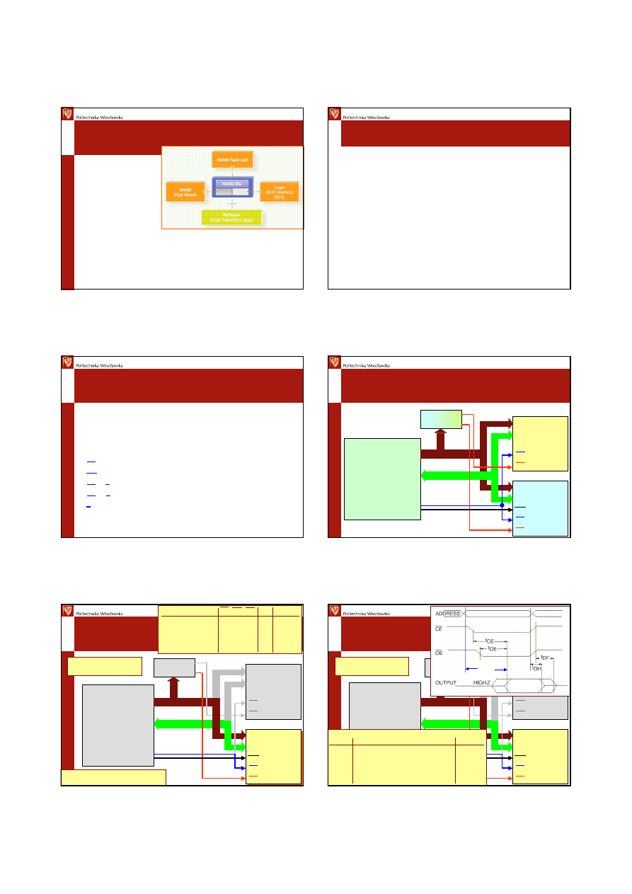
Fusion Memory
As
consumers continue their insatiable demand for higher-performance,
ever-smaller mobile devices
, Samsung’s fusion memory products are
increasingly chosen by handheld designers.
These
fusion semiconductors integrate different memory technologies
and can also include logic, software and other elements on a single
chip
. Samsung’s fusion products simplify device architecture, reduce power
consumption, increase performance and cut costs while enabling mobile
products to be smaller and deliver greater functionality than ever.
Samsung as the world memory
leader and a strong player in mobile logic
chips, Samsung has exploited its considerable expertise in technologies and
processes to create its fusion memory offerings.
These chips are optimal for
today’s fast-selling consumer products, from mobile phones, portable
media players and digital cameras to personal navigation devices and
multi-function handhelds
.
Samsung Fusion Memory. The Next-Generation Technology for High-Performance
Mobile Applications. Samsung Semiconductor, December 2007
2
OneNAND Flash
(NAND core + NOR interface logic + SRAM buffer)
Samsung Fusion Memory. The Next-Generation Technology for High-Performance
Mobile Applications. Samsung Semiconductor, December 2007
•
The highest-performance flash on the market
•
Included in dozens of different mobile products
•
Has program/erase performance of NAND with NOR’s read performance
•
Can improve booting speed of mobile phones by as much as 20 percent
•
uses up to 60 percent less energy than competing NOR memory
Memory Parameter
(www.st.com
→
→
→
→
Memories)
Memory Size
– [Storage Capacity] The amount of data that can be contained in a
storage device measured in binary characters, bytes, words, or other units of
data. IEEE Std. 610.10-1994.
Supply Voltage
(V
CC
) - the value as specified by level (minTypMax) of the direct
supply voltage, applied to an IC. IEC61360-AAE690 (V
CC
).
Memory Organization
- Shown as a text representation of the Memory
Organization (i.e. 512 x 8).
Access Time
(t
ACC
) - time of address to output delay.
Chip Enable
To Output Delay (t
CE
) - time of chip enable to output delay.
Output Enable
To Output Delay(t
OE
) - time of output enable to output delay.
Programming Voltage
(V
PP
) /
Current
(I
PP
) - Programming voltage or current by
the specified test condition
Standby Supply Voltage Current
CMOS(I
CC2
)-Operating supply current by the
specified test condition.
Operating Temperature
- The value as specified by level (minTypMax) of the
ambient temperature (in Cel) in which this item was designed to operate.
Memory
Signal Names
V
CC
– Supply Voltage
V
SS
– Ground
V
PP
– Program Supply
A
0
.. A
XX
(Addr) – Address Inputs
D
0
.. D
XX
or
Q
0
.. Q
XX
(Data) – Data Inputs / Outputs
RD
– Data Read
WR
– Data Write
CS
or
E
– Chip Select / Enable
OE
or
G
– Output Enable
P
– Program
NC
– Not Connected Internally
DU
– Don’t Use
Microprocessor
&
&
&
&
Memory
Address
Decoder
ROM
Memory
RAM
Memory
Addr
Data
OE
CS
Addr
Data
OE
CS
WE
Address Bus
Microprocessor
Microcontroller
Addr
Data
Data Bus
RD
WR
Single CS#
Memory
Select
Address
Decoder
Memory
Flash
Memory
Addr
Data
OE
CS
Addr (A
15..0
)
Data (IO
7..0
)
OE
CS
WE
Address Bus
Microprocessor
Microcontroller
Addr
Data
Data Bus
RD
WR
Single CS#
MODE
CE OE WE Ai
I/O
Standby/Write Inhibit H
X
X
X
High Z
Output disable
X
H
X
High Z
Read
L
L
H
Ai
D
OUT
Program
L
H
L
Ai
D
IN
I
SB1
V
CC
Standby Current < 50
µ
A
I
CC
V
CC
Active Current
< 15 mA
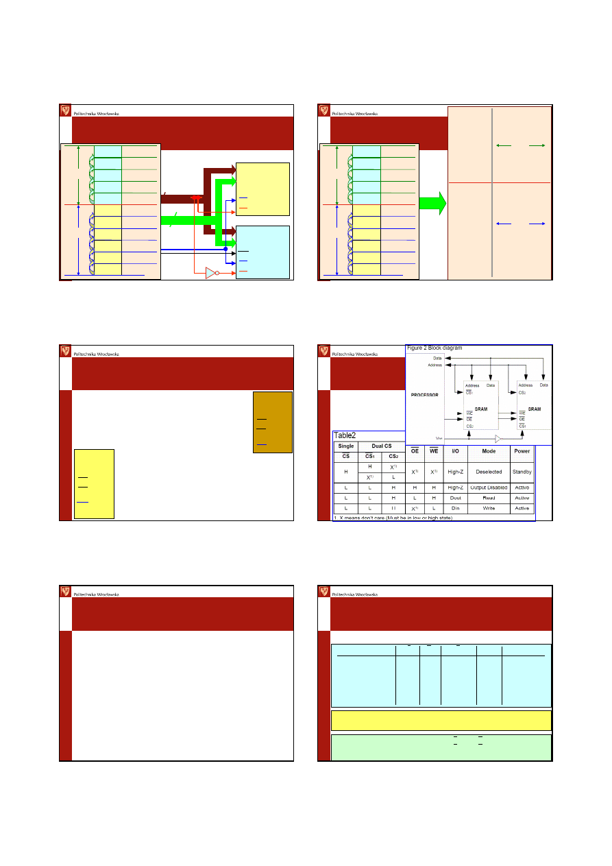
AT29LV512 . 512K (64Kx8)
3-volt Only Flash Memory.
Atmel, 0177O–FLASH–9/08
Memory
Read Waveforms
Address
Decoder
Memory
Flash
Memory
Addr
Data
OE
CS
Addr (A
15..0
)
Data (IO
7..0
)
OE
CS
WE
Address Bus
Microprocessor
Microcontroller
Addr
Data
Data Bus
RD
WR
Single CS#
AT29LV512 . 512K (64Kx8)
3-volt Only Flash Memory.
Atmel, 0177O–FLASH–9/08
AC Read Characteristics AT29LV512-
12
Symbol Parameter
Units
t
ACC
Address to Output Delay
.. 120 ns
t
CE
CE to Output Delay
.. 120 ns
t
OE
OE to Output Delay
0 .. 50 ns
t
DF
CE or OE to Output Float
0 .. 30 ns
t
OH
Output Hold from OE, CE
0 .. ns
or Address, whichever occurred first
Access Time
t
ACC
Address Valid
Output
Valid
3
Memory Address
Decoder
(1/2)
ROM
Memory
4Kx8
RAM
Memory
4Kx8
Addr
11..0
Data
7..0
OE
CS
Addr
11..0
Data
7..0
OE
CS
WE
Address Bus
Microprocessor
Microcontroller
Addr
Data
Data Bus
RD
WR
A
15
16
8
0000h
ROM (1)
ROM (2) 1000h
ROM (3) 2000h
6000h
ROM (8) 7000h
RAM (1) 8000h
RAM (2) 9000h
ROM (7)
.........
E000h
RAM (8) F000h
RAM (7)
.........
A
15
= 0
A
15
= 1
FFFFh
EFFFh
DFFFh
9FFFh
8FFFh
7FFFh
6FFFh
5FFFh
2FFFh
1FFFh
0FFFh
FFFFh=
1
111
1111 1111 1111b
F000h =
1
111
0000 0000 0000b
EFFFh=
1
110
1111 1111 1111b
E000h =
1
110
0000 0000 0000b
9FFFh=
1
001
1111 1111 1111b
9000h =
1
001
0000 0000 0000b
8FFFh=
1
000
1111 1111 1111b
8000h =
1
000
0000 0000 0000b
7FFFh=
0
111
1111 1111 1111b
7000h =
0
111
0000 0000 0000b
6FFFh=
0
110
1111 1111 1111b
6000h =
0
110
0000 0000 0000b
2FFFh=
0
010
1111 1111 1111b
2000h =
0
010
0000 0000 0000b
1FFFh=
0
001
1111 1111 1111b
1000h =
0
001
0000 0000 0000b
0FFFh=
0
000
1111 1111 1111b
0000h =
0
000
0000 0000 0000b
0000h
ROM (1)
ROM (2) 1000h
ROM (3) 2000h
6000h
ROM (8) 7000h
RAM (1) 8000h
RAM (2) 9000h
ROM (7)
.........
E000h
RAM (8) F000h
RAM (7)
.........
A
15
= 0
A
15
= 1
FFFFh
EFFFh
DFFFh
9FFFh
8FFFh
7FFFh
6FFFh
5FFFh
2FFFh
1FFFh
0FFFh
Memory Address
Decoder
(2/2)
A
15
A
15
A
11 .. 0
A
11 .. 0
Single CS SRAM
&
dual CS SRAM
if you take
dual CS
products, you can reduce
board area because
you do not need
additional component
dual CS
products represent frexibility of system
design, which
adopt battery backup mode
TNAL9803. BENEFIT OF DUAL CS. TECHNICAL NOTE
SAMSUNG Electronics CO., LTD. 1998
CS
WE
OE
Addr
Data
SRAM
CS1
WE
OE
CS2
Addr
Data
SRAM
if system has more than one SRAM or controller can
not drive CS to high at power down mode
,
you
need additional component
on PCB for Data
Retention mode
Dual CS
SRAM
If system has more than one SRAM or controller can not drive CS
to high at power down mode, you need additional component on
PCB for Data Retention mode
if you take dual CS products, you can reduce board area because
you do not need additional component
Dual CS products represent frexibility of system design, which
adopt battery backup mode
EPROM / OTP EPROM
EPROM
(
E
lectrically
P
rogrammable
R
ead
O
nly
M
emory) is a nonvolatile
memory which offers the ability to both program and erase the contents
of the memory multiple times.
An EPROM must be
programmed
using a
12.5 volt
(or higher) PROM
programmer, and then transferred into the system in which it is intended
to function.
EPROMs can be
erased
by shining
ultraviolet light
into the window in
the top of the IC package. The process of writing data into an EPROM
and then erasing it may be repeated almost indefinitely. EPROMs are
usually used for product development, and later replaced with less
expensive one–time programmable EPROMs.
OTP
EPROM:
O
ne–
T
ime
P
rogrammable EPROM. An EPROM which
can only be written with code/data once instead of multiple times.
Generally, OTP EPROMs are less expensive then erasable EPROMs.
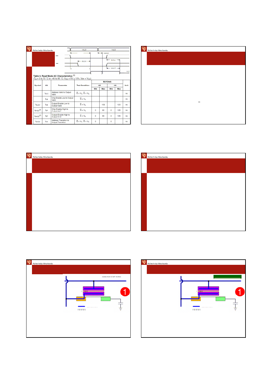
EPROM
Parameters
Mode
E
G
P
V
PP
Q Output
Read
V
IL
V
IL
V
IH
V
CC
Data Out
Output Disable
V
IL
V
IH
V
IH
V
CC
Hi-Z
Program
V
IL
X
V
IL
Pulse
V
PP
Data Input
Verify
V
IL
V
IL
V
IH
V
PP
Data Output
Standby
V
IH
X
X
V
CC
Hi-Z
M27C64A. 64 Kbit (8Kbit x 8) UV EPROM and OTP EPROM.
STMicroelectronics, October 2002
C
IN
Input Capacitance
V
IN
= 0V
6 pF
MAX
C
OUT
Output Capacitance
V
OUT
= 0V
12 pF
MAX
I
CC
Supply Current
E = V
IL
G = V
IL
30 mA
MAX
I
CC1
Supply Current (Standby) TTL
E = V
IH
G =
X
1 mA
MAX
I
CC2
Supply Current (Standby) CMOS
E > V
CC
– 0.2V
100
µ
A
MAX
4
EPROM
Timing
Q0-Q7
G
E
A0-Q12
250
250
300
300
t
AVQV
t
AVQV
t
ELQV
t
ELQV
EPROM
Erasure Operation
When delivered (and after each erasure for UV EPROM), all bits of the
M27C64A are in the "1” state.
Data is introduced by selectively programming "0"s into the desired bit
locations. Although only "0"s will be programmed, both "1"s and "0"s can
be present in the data word.
The only way to change a "0" to a "1" is by die exposition to ultraviolet
light (UV EPROM). The M27C64A is in the programming mode when
VPP input is at 12.5V, E is at V
IL
and P is pulsed to V
IL
.
The data to be programmed is applied to 8 bits in parallel to the data
output pins. The levels required for the address and data inputs are TTL.
V
CC
is specified to be 6V ± 0.25V.
erasure begins when the cells are exposed to
light with
wavelengths shorter
than approximately
4000 Å
; it should be noted that sunlight and some type of
fluorescent lamps
have wavelengths in the
3000-4000 Å
range
research shows that constant exposure to
room
level
fluorescent
lighting
could
erase
a typical M27C64A in about
3 years
, while it would take
approximately
1 week
to cause erasure when exposed to direct
sunlight
recommended
erasure procedure for the M27C64A is exposure to short
wave ultraviolet light which has a
wavelength
of
2537 Å
integrated dose (i.e. UV
intensity
x exposure time) for erasure should be a
minimum of
15 W-sec/cm
2
; erasure time with this dosage is approximately
15 to 20 minutes
using an ultraviolet lamp with
12000
µ
W/cm
2
power rating -
M27C64A should be placed within
2.5 cm
(1 inch) of the lamp tubes during
the erasure
EEPROM - Flash Memory
EEPROM
:
•
erase the entire device all at once
•
program or write
single bytes
at a time
Flash
is a high-speed EEPROM:
•
program and erase
BLOCKS
of data at a time
EEPROM
AT25128/AT25256. SPI Serial Automotive EEPROMs 128K (16,384 x 8) / 256K (32,768 x 8)
Atmel Corporation 2002, Rev. 3262A–SEEPR–02/02
Serial Peripheral Interface (SPI) Compatible
Medium-voltage and Standard-voltage Operation
– 5.0 (VCC = 4.5V to 5.5V)
– 2.7 (VCC = 2.7V to 5.5V)
3 MHz Clock Rate
64-byte Page Mode and Byte Write Operation
Block Write Protection – Protect 1/4, 1/2, or Entire Array
Write Protect (WP) Pin and Write Disable Instructions for both Hardware and
Software Data Protection
Self-timed Write Cycle (5 ms Typical)
High-reliability
– Endurance: 100,000 Write Cycles
– Data Retention: >200 Years
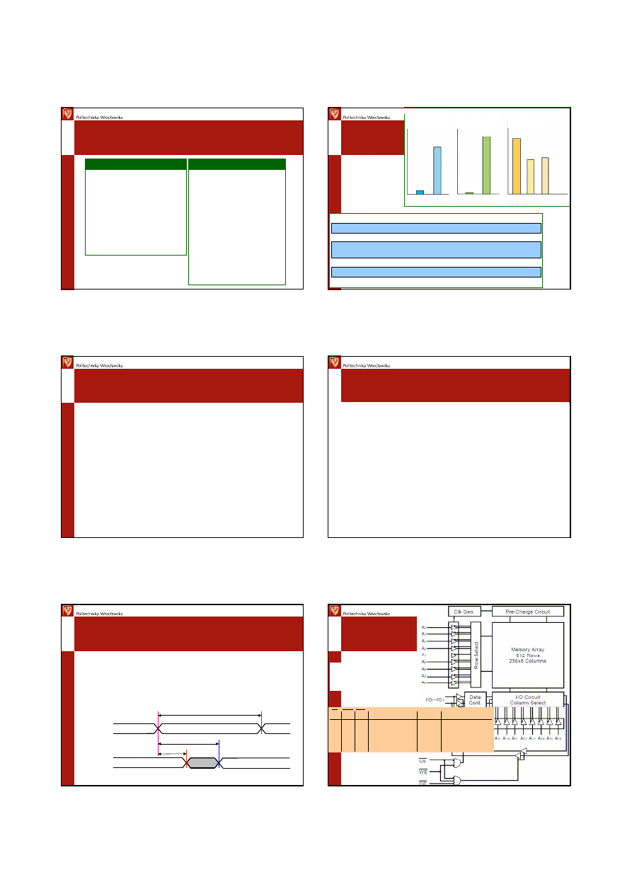
EEPROM
(Electronically Erasable Programmable Read Only Memory)
EEPROM
has a grid
of columns and rows
with a cell that has
two transistors at
each intersection
transistors are sepa-
rated from each other
by a thin
oxide layer
transistors is known
as a
Floating Gate
and
Control Gate
as long as this link is in place, the cell has a value of 1 – to change the value
to a 0 requires a curious process called
Fowler-Nordheim tunneling
tunneling
(and
erasing
) is used to alter the placement of electrons in the
floating gate (an electrical charge, usually 10 to 13 volts, is applied to the
floating gate) – the charge comes from the column, or
bitline
, enters the
floating gate and drains to a ground
Thin Oxide
Layer
Thin Oxide
Layer
Word Line
B
it
L
in
e
http://electronics.howstuffworks.com/flash-memory.htm
Control
Gate
Floating
Gate
Source
Drain
Current flow
Negatively charged
electrons
http://electronics.howstuffworks.com/flash-memory.htm
EEPROM
Tunneling
charge
causes the
floating-gate transistor to
act like an
electron gun
excited
electrons
are
pushed
through and
trapped on other side of
the thin oxide layer, giving
it a
negative charge
these
negatively
charged electrons
act as
a
barrier
between the control gate called a cell sensor monitors the level of
the charge passing through the floating gate
if the
flow
through the gate
is above the 50 percent
threshold, it has a value
of
1
– when the
charge
passing through
drops below the 50-percent
threshold, the value changes to
0
blank
EEPROM has all of the gates fully open, giving each cell a value of
1
Thin Oxide
Layer
Thin Oxide
Layer
Word Line
B
it
L
in
e
Control
Gate
Floating
Gate
Source
Drain
Current flow
Negatively charged
electrons
HOW STUFF WORKS
5
NAND / NOR Comparison
Jim Cooke: ESC-225 NAND 101. An Introduction to NAND Flash and How to Design
it into Your Next Product. Micron Technology, Inc.
April 4 2006
• Advantages:
– Fast writes
– Fast erases
• Disadvantages:
– Slow random access
– Byte writes difficult
• Applications:
– File (disk) applications
– Voice, data, video recorder
– Any large sequential data
• Advantages:
– Random access
– Byte writes possible
• Disadvantages:
– Slow writes
– Slow erase
• Applications
– Replacement of EPROM
– Execute directly from
nonvolatile memory
NOR
NAND
Figure 4: NAND/NOR comparison
NOR
vs
NAND
Programming
unit:
µµµµ
s/Byte
Erasing
unit:
µµµµ
s/Byte
Read
unit:
µµµµ
s/Byte
NAND NOR
NAND NOR
NAND
x8
NOR
NAND
x16
NAND
NOR
Capacity
1 Gbit x chip
128 Mbit per chip
Power Supply
2,7 – 3,6 V
2,3 – 3,6 V
Access Time
50 ns (serial access cycle) 70 ns (30pF; 2,3V)
25
µµµµ
s (random access)
65 ns (30pF, 2,7V)
Programm Speed (typ)
200
µµµµ
s / 512 Byte
8
µµµµ
s / Byte
Erase Speed (typ)
2 ms / Block (16 KB)
4,1 ms / 512 Byte
Prog + Erase (typ)
33,6 ms / 64 KB
700 ms / Block
6,0
0,4
0,12
15,2
69
44
45
SRAM
(
S
tatic
R
andom
A
ccess
M
emory)
is essentially a
stable DC flip–flop
requiring no clock timing or
refreshing
contents
of an
SRAM
memory are retained
as long as power is
supplied
SRAMs
support extremely
fast access times
SRAMs
also have relatively few strict timing requirements and a
parallel address structure,
making
them particularly suited
for
cache
and other low–density, frequent–access applications
NV SRAM
(
N
on
V
olatile
S
tatic
R
andom
A
ccess
M
emory)
NV SRAM
is a single package which contains a
low–power SRAM
, a
nonvolatile memory controller, and a
lithium type battery
when the
power supply
to this single modular package
falls
below the
minimum requirement to maintain the contents of the SRAM, the
memory
controller in the module switches the power supply from the external
source to the internal lithium battery
and write
protects
the
SRAM
these
transitions
to and from the external power source are
transparent
to
the SRAM, making it a true nonvolatile memory
this unique construction combines the strategic
advantages
of SRAM–
addressing structure, high–speed access, and timing requirements – with the
nonvolatility advantages of EEPROM technologies
Battery–backed SRAM modules from Dallas Semiconductor are
pin
–
compatible
with non–battery–backed SRAMs, making them ideal for any
application where a traditional SRAM would be suitable
SRAM
Single Access Read Cycle
t
RC
t
RC
Read Cycle Time
t
AA
Address Access Time
t
OH
Output
Hold from Address Change
t
OH
t
AA
Data Valid
Previous Data Valid
Data Out
Address
???
SRAM
K6R1008V1D (1/3)
K6R1008V1D.
1Mbit Asynchronous Fast SRAM
High-Speed CMOS Static RAM.
Samsung Electronics June 2003
A0 - A16
Address Inputs
WE
Write Enable
CS
Chip Select
OE
Output Enable
I/O1 ~ I/O8
Data Inputs/Outputs
VCC
Power(+3.3V)
VSS
Ground
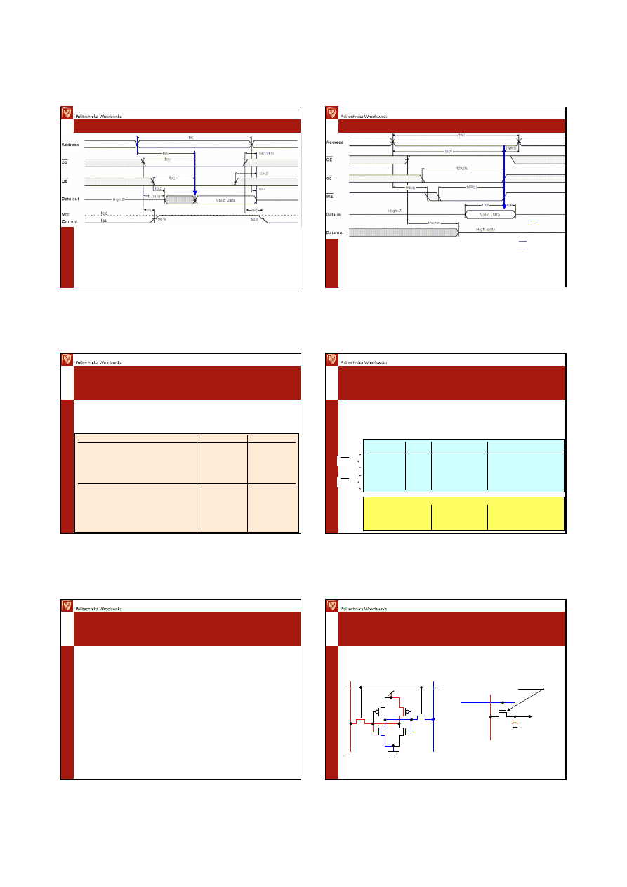
CS WE OE Mode
I/O Pin Supply Current
H
X
X* Not Select
High-Z ISB, ISB1
L
H H Output Disable High-Z ICC
L
H
L
Read
DOUT ICC
L
L
X
Write
DIN
ICC
6
SRAM - READ
K6R1008V1D-08 (2/3)
Read Cycle Time
t
RC
8 ns
MIN
Address Access Time
t
AA
8 ns
MAX
Chip Select to Output
t
CO
8 ns
MAX
Output Enable to Valid Output
t
OE
4 ns
MAX
Output Hold from Address Change
t
OH
3 ns
MIN
Chip Selection to Power Up Time
t
PU
0 ns
MIN
Chip Selection to Power DownTime
t
PD
8 ns
MAX
K6R1008V1D. 1Mbit Asynchronous Fast SRAM High-Speed CMOS Static RAM.
Samsung Electronics June 2003
SRAM - Write
K6R1008V1D-08 (3/3)
Write Cycle Time
t
WC
8 ns
MIN
Chip Select to End of Write
t
CW
6 ns
MIN
Address Set-up Time
t
AS
0 ns
MIN
Address Valid to End of Write
t
AW
6 ns
MIN
Write Pulse Width(OE High)
t
WP
6 ns
MIN
End of Write to Output Low-Z
t
OW
3 ns
MIN
(OE= Clock)
(OE=Low Fixed)
(CS = Controlled)
K6R1008V1D. 1Mbit Asynchronous Fast SRAM High-Speed CMOS Static RAM.
Samsung Electronics June 2003
Memory
&
&
&
&
Memory
Dynamic
K6R1008V1D-08
K6F1008V2C-55
Read Cycle Time
t
RC
8 ns
MIN
55 ns
MIN
Address Access Time
t
AA
8 ns
MAX
55 ns
MAX
Chip Select to Output
t
CO
8 ns
MAX
55 ns
MAX
Output Enable to Valid Output
t
OE
4 ns
MAX
25 ns
MAX
Output Hold from Address Change
t
OH
3 ns
MIN
10 ns
MIN
Write Cycle Time
t
WC
8 ns
MIN
55 ns
MIN
Chip Select to End of Write
t
CW
6 ns
MIN
45 ns
MIN
Address Set-up Time
t
AS
0 ns
MIN
0 ns
MIN
Address Valid to End of Write
t
AW
6 ns
MIN
45 ns
MIN
Write Pulse Width(OE High)
t
WP
6 ns
MIN
40 ns
MIN
End of Write to Output Low-Z
t
OW
3 ns
MIN
5 ns
MIN
K6R1008V1D. 1Mbit Asynchronous Fast SRAM High-Speed CMOS Static RAM.
Samsung Electronics June 2003
K6F1008V2C. 128Kx8 bit Super Low Power and Low Voltage CMOS Static RAM.
Samsung Electronics, March 2005
F
A
ST
SL
O
W
Memory
&
&
&
&
Memory
Static
Parameter Symbol
K6R1008V1D-08
K6F1008V2C-55
Operating
I
CC2
90 mA
35 mA
MAX
TTL
Current
I
CC1
3 mA
MAX
CMOS
Standby
I
SB
20 mA
TTL
Current
I
SB1
5 mA
5
µ
A
MAX
CMOS
Input/Output Capacitance
C
I/O
8 pF
MAX
10 pF
MAX
Input Capacitance
C
IN
6 pF
MAX
8 pF
MAX
CS=1
CS=0
K6R1008V1D. 1Mbit Asynchronous Fast SRAM High-Speed CMOS Static RAM.
Samsung Electronics June 2003
K6F1008V2C. 128Kx8 bit Super Low Power and Low Voltage CMOS Static RAM.
Samsung Electronics, March 2005
F
A
ST
SL
O
W
DRAM
(
D
ynamic
R
andom
A
ccess
M
emory)
in an
SRAM
, this information is stored in a
four to six transistor flip–
flop
which is easy to address, but requires a relatively large memory
cell
DRAM
, by comparison, stores its 1 or 0 as a charge on a
small
capacitor
, requir ing much more current then an SRAM to maintain the
stored data
net
memory cell size
is
smaller
for the
DRAM
than for the SRAM, so
the total cost per bit of memory is less
DRAM’s capacitors must be
constantly
refreshed
so that they retain
their charge
DRAMs require more sophisticated interface circuitry
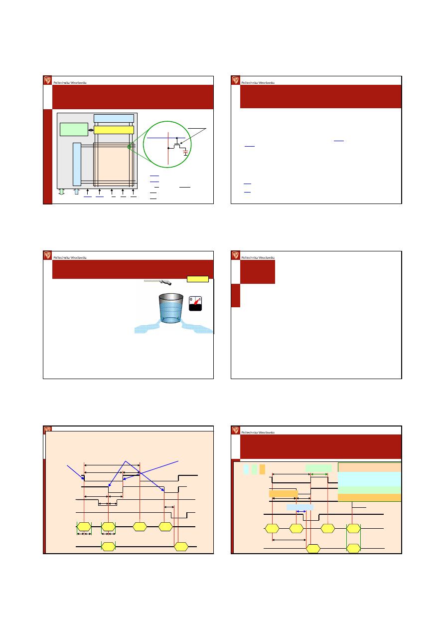
SRAM / DRAM Cell
bit = 1
bit = 0
Select = 1
On
Off
Off
On
N1
N2
P1
P2
On
On
Word Line
Bit
Line
Storage
element
(capacitor)
Switching
element
SRAM Cell
DRAM Cell
C = 0,020 – 0,040 pF
C
Sense
Amplifier
7
DRAM Architecture
Word Line
Bit
Line
Storage
element
(capacitor)
Switching
element
DRAM Cell
Memory
Array
.. Bit Lines ..
..
W
o
rd
L
in
e
s
.
.
R
o
w
D
e
c
o
d
e
r
Column Decoder
Data In/Out
Buffers
Sense Amps
RAS CAS
R/W
OE
Addr
Data
RAS – Row Access Select
CAS – Column Access Select
R/W – Read / Write
OE – Output Enable
CS – Chip Select
CS
DRAM
Memory Circuits
Memory Controller
include a series of tasks that include identifying the type,
speed and amount of memory and checking for errors
memory cells
have a whole support infrastructure of other specialized circuits
to perform functions:
–
address logic to select rows and columns
:
RAS
(Row Address Select) and
CAS
(Column Address Select)
–
internal
Refresh Counters
or registers to keep track of the refresh
sequence, or to initiate refresh cycles as needed
–
Sense Amplifier
to amplify the signal or charge detected on a memory
cell
–
WE
(Write Enable) telling a cell whether it should take a charge or not
–
OE
(Output Enable) logic to prevent data from appearing at the outputs
unless specifically desired.
Understanding DRAM Operation.
Applications Note. IBM, December 1996
DRAM
Refresh
milliseconds
a full bucket becomes
empty
CPU
or the
memory controller
has to come along and
recharge all
of the
capacitors holding
a
1
before they discharge – to do this, the memory
controller reads the memory and then writes it right back
refresh operation
happens automatically thousands of times per second
http://computer.howstuffworks.com/ram.htm
capacitor
is like a small bucket that is
able to store electrons
to
store
a
1
in the memory cell, the
bucket is
filled with electrons
to
store
a
0
, it is
emptied
problem with the
capacitor's
bucket is
that it has a
leak
, in a matter of a
few
Refresh
DRAM
Refresh
each cell unit consisting of a transistor and a very small
capacitor
of about
20-40 fF
(Femtofarad, 0.020-0.040 pF) - a charged capacitor has a logical 1,
a discharged capacitor a logical 0
DRAM
must
refresh
the row each time the spec t
REF
is elapsed
Micron Technology:
refresh period t
REF
= 32 / 64 ms (2,048 / 4,096 cycles)
Samsung Electronics (
Auto refresh
)
:
refresh period t
REF
= 64 ms (4K cycles)
3
different
refresh modes
are available:
RAS only Refresh, Hidden Refresh, CAS before RAS Refresh
Robert Hoffmann: Engineer To Engineer. Note EE-126.
European DSP Applications. Analog Devices, Rev1 (20-March-02)
TN-04-30. VARIOUS METHODS OF DRAM REFRESH
Micron Technology, Rev. 2/1999
AN987. DRAM Refresh Modes.
Motorola Semiconductors. REV 1. February 1994
MT4LC4M4E8, MT4LC4M4E9. 4 MEG x 4 EDO DRAM
.
Micron Technology Rev. 6/1998
K4S64xx32N Synchronous DRAM. 2M x 8Bit x 4Banks / 1M x 16Bit x
4Banks SDRAM
.
Samsung Electronics, Rev. 1.12 August 2008
DRAM
- timing
Engineer To Engineer. Note EE-126 Contributed by Robert Hoffmann,
European DSP Applications. Analog Devices, Rev1 (20-March-02)
1. Activation:
–
bias the row’s bit lines
–
sense the word lines’
capacitor cells
–
store sensed value
statically
2. Access Column:
–
select bit lines
–
WR: write to sense amp
–
RD: read stored value
3. Precharge:
–
write stored value back to
the cell
–
deselect row and columns
t
RC
t
RAS
t
RP
t
CAS
t
RCD
t
WCS
t
WCH
t
CAC
t
ARS
t
ARH
~RAS
~CAS
~WE
~OE
Address
Data
D
Q
Col
Row
Row
t
ACS
t
ACH
Col
Idle state
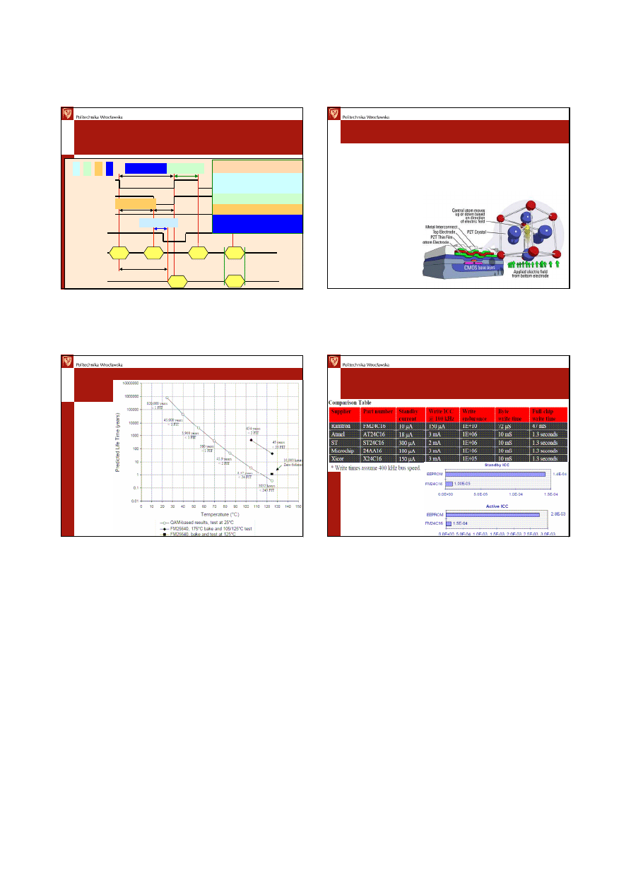
What does 4-3-3 SDRAM mean
t
RP
= 20 ns
t
CAS
~RAS
~CAS
~WE
~OE
Address
Data
D
Col
Row
Row
Col
Idle state
Q
t
RAS
4
–
3
–
3
t
RAC
t
CAC
= 25 ns
t
RCD
= 20 ns
t
CLK
= 7,5 ns (133 MHz Bus)
t
RCD
/ t
CLK
= 2,67
→
→
→
→
3
t
RP
/ t
CLK
= 2,67
→
→
→
→
3
CL = t
CAC
/ t
CLK
= 3,33
→
→
→
→
4
CL is CAS Latency
8
What does 2-3-3-6-1T DRAM mean
t
RP
= 20 ns
t
CAS
~RAS
~CAS
~WE
~OE
Address
Data
D
Col
Row
Row
Col
Idle state
Q
t
RAS
= 40 ns
t
RAC
t
CAC
= 15 ns
t
RCD
= 20 ns
t
CLK
= 7,5 ns (133 MHz Bus)
t
RCD
/ t
CLK
= 2,67
→
→
→
→
3
t
RP
/ t
CLK
= 2,67
→
→
→
→
3
CL = t
CAC
/ t
CLK
= 2
→
→
→
→
2
CL is CAS Latency
2
–
3
–
3
–
6
t
RAS
/ t
CLK
= 5,33
→
→
→
→
6
Bank cycle time
FRAM Operation
ferroelectric crystal has a mobile atom in the center of the crystal
,
applying an electric field across a face of the crystal causes this atom to move
in the direction of the field
reversing
the
field
causes the
atom to move
in the
opposite direction
atom positions at the top and bottom of the crystal are stable
removing
the
electric field
leaves
the
atom in a
stable position
, even in the
absence of power
as a memory element, the
ferroelectric crystal creates
an
ideal digital memory
- it
contains two stable data
states, it requires very little
time and energy to change
states, and is very stable
over a variety of
environmental conditions
FRAM
Sun S. Sommervold B. Culbreth T. Davenport T: Data Retention Performance of 0.5
µ
m
FRAM Products. Technical paper, Ramtron, Apr. 2006
Advantages of the FRAM Memory
AN-200. Advantages of the FM24C16 Serial 16Kb FRAM Memory.
Ramtron, Jan. 1999
Wyszukiwarka
Podobne podstrony:
6 Pamieci ROM RAM id 43808 Nieznany
Pamięci ROM i RAM w komputerze, wrzut na chomika listopad, Informatyka -all, INFORMATYKA-all, Inform
6 Pamieci ROM RAM 2015 www
Pamięci dynamiczne RAM, Szkoła, Systemy Operacyjnie i sieci komputerowe, utk, semestr I
TI temat 17 ROM RAM
ROM RAM
F2 65 Pamięci statyczne RAM 3
ROM i RAM
Pamięci dynamiczne RAM, Szkoła, Systemy Operacyjnie i sieci komputerowe, utk, semestr I
USB niekompatybilne z ReadyBoost Możliwość wykorzystania tanich przenośnych pamięci USB jako rozs
Pamięć ROM
Pamięć RAM ROM
Pamieci RAM ROM
co to jest pamięć ram, rom, hdd,?d, floppy, partycja, katalog, plik LHBD5E3LSXW26LJNUOWZ374VUUBOA5E
Pamięć RAM i ROM, Studia, Informatyka, Informatyka, Informatyka
więcej podobnych podstron