
© Motorola, Inc., 1988, 2000
AN1010
Order this document
by AN1010/D
Motorola Semiconductor Application Note
AN1010
MC68HC11 EEPROM Programming
from a Personal Computer
Introduction
This application note describes a simple and reliable method of
programming either the MC68HC11’s internal EEPROM or the
EEPROM connected to the MCU’s external bus.
The data to be programmed is downloaded from any standard personal
computer (PC) fitted with a serial communications port. In addition to the
programming procedure, the software incorporates the facility to verify
the contents of the MCU’s internal or external memory against code held
on a PC disc. Both program and verify options use data supplied in S
record format, which is downloaded from the PC to the MC68HC11
using the RS232 protocol supported by the MCU’s SCI port.
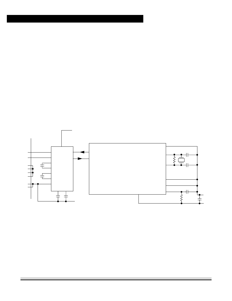
The minimum MCU configuration required to program the MC68HC11’s
internal EEPROM is shown in
. This consists only of the MCU,
an RS232 level-shifting circuit, plus an 8-MHz crystal and a few passive
components.
To initiate the download, the PC is connected to the MC68HC11 SCI
transmit and receive lines via a level shifter. The circuit in
uses
a Maxim MAX232 to eliminate the need for additional
±
12-volt supplies.
The MCU’s special bootstrap mode is invoked by applying a logic 0 to
the MODA and MODB pins, followed by a hardware reset.
Removing the reset condition causes the MCU to start execution of its
bootloader program, located in internal ROM, between addresses
$BF40 and $BFFF. In normal single-chip or expanded modes, the boot
Application Note
AN1010
2
MOTOROLA
ROM is not accessible, and reads from these memory locations will
result, respectively, in irrelevant data or external memory fetches.
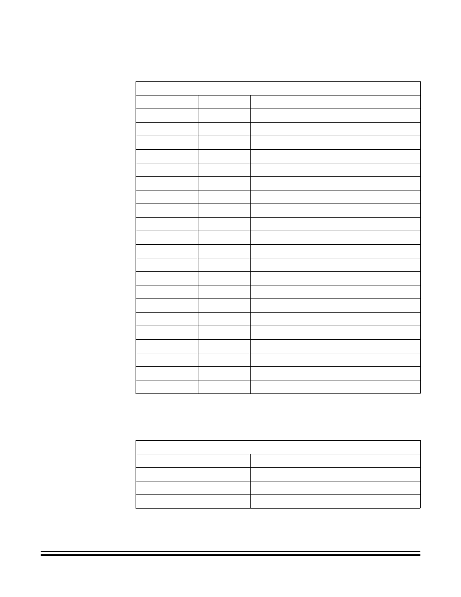
An additional consequence of bootstrap operation is that all vectors are
relocated to the boot ROM area. With the exception of the reset vector,
which points to the start of the boot ROM, the remaining interrupt vectors
all point to an uninitialized jump table in RAM. Three bytes are reserved
for each entry in the jump table to allow for an extended jump instruction.
and
detail the memory map of the bootstrap vectors and
an example RAM jump table.
Note that before any interrupts are enabled in bootstrap mode, it is the
software designer’s responsibility to initialize all appropriate entries in
the jump table.
As this application note does not make use of the MC68HC11’s interrupt
system, the jump table is not set up.
Figure 1. MC68HC11 Bootstrap Mode Connection to RS232 Line
MAX232
MC68HC11A1
52-PIN PLCC
+
+
0 V
C4
C3
2
6
RS232
CONNECTOR
RxD
TxD
0 V
+
+
C1
C2
CTS
DSR
DCD
DTR
GND
14
13
1
3
4
5
15
16
+5 V
11
21
12
20
PD1 (TX)
PD0 (RX)
+5 V
26
V
DD
1
7
8
3
2
17
V
SS
EXTAL
XTAL
MODA
MODB
RESET
10 M
22 pF
8 MHz
22 pF
4.7 k
1
µ
F
0 V
0.1
µ
F
CERAMIC
C1, C2, C3, C4 — 22 mF, 25-V aluminum or tantalum
Note: To improve reliability of the MCU, all its unused inputs should be connected to V
SS
or V
DD
.
Application Note
Introduction
AN1010
MOTOROLA
3
Table 1. Bootstrap Vector Assignments
Boot ROM
Address
Vector
Description
BFFE
BF40
Bootstrap reset
BFFC
00FD
Clock monitor
BFFA
00FA
COP fail
BFF8
00F7
Illegal opcode
BFF6
00F4
SWI
BFF4
00F1
XIRQ
BFF2
00EE
IRQ
BFF0
00EB
Real-time interrupt
BFEE
00E8
Timer output capture 1
BFEC
00E5
Timer output capture 2
BFEA
00E2
Timer output capture 3
BFE8
00DF
Timer output compare 1
BFE6
00DC
Timer output compare 2
BFE4
00D9
Timer output compare 3
BFE2
00D6
Timer output compare 4
BFE0
00D3
Timer output compare 5
BFDE
00D0
Timer overflow
BFDC
00CD
Pulse accumulator overflow
BFDA
00CA
Pulse accumulator input edge
BFD8
00C7
SPI
BFD6
00C4
SCI
Table 2. RAM Jump Table
Internal RAM
Address
Typical Instruction
00FD
JMP CLKMON
00FA
JMP COPFL
. . . etc.

Application Note
AN1010
4
MOTOROLA
The bootstrap program continues by initializing the SCI transmitter and
receiver to 7812 baud and proceeds to examine the state of the NOSEC
bit in the CONFIG register. If this is at logic 0 (security enabled), the
bootloader will erase the entire contents of internal EEPROM and also
the CONFIG register.
This feature is particularly useful for security-conscious applications,
where the internal EEPROM contains information of a proprietary or
confidential nature. If the NOSEC bit is at logic 1, then the erasing
sequence is not carried out.
Note also that erasing the CONFIG register disables the security feature.
The bootstrap program then issues a break condition on the SCI transmit
line and waits for the reception of the first byte. In this application, no use
is made of the break transmitted by the SCI.
At this point, it is necessary to initiate the PC S record downloader
program, called EELOAD.BAS (written in BASIC). It will display a header
message and prompt the user for the number of the COM channel
(either one or two) which is connected to the MC68HC11. A listing of
EELOAD.BAS is given at the end of this application note.
The PC-resident program will now configure the appropriate COM
channel to 1200 baud, one stop bit, no parity, and download the binary
file EEPROGIX.BOO from the PC to the MC68HC11.
The MC68HC11’s bootloader automatically will detect the fact that the
first incoming character is received at a different baud rate and change
its SCI rate to 1200 baud.
It will then proceed to load the binary file into all 256 RAM locations and
then jump to address $0000 (for instance, the first RAM location).
EEPROGIX.BOO consists of the MC68HC11 executable code shown in
the source listing at the end of this application note, with the addition of
$FF at the head of the file, and $00 appended up to the 256th byte. This
program is designed to receive S records from the PC and program the
data fields into the appropriate EEPROM memory locations.
Application Note
Introduction
AN1010
MOTOROLA
5
A point to note is that the initial $FF byte in EEPROGIX.BOO is only used
to detect the baud rate of the PC and is not echoed back, while the
remaining 256 bytes are echoed by the MC68HC11’s SCI transmitter.
However, during download of EEPROGIX.BOO, the PC does not detect
the echo, as this feature is unnecessary at this stage.
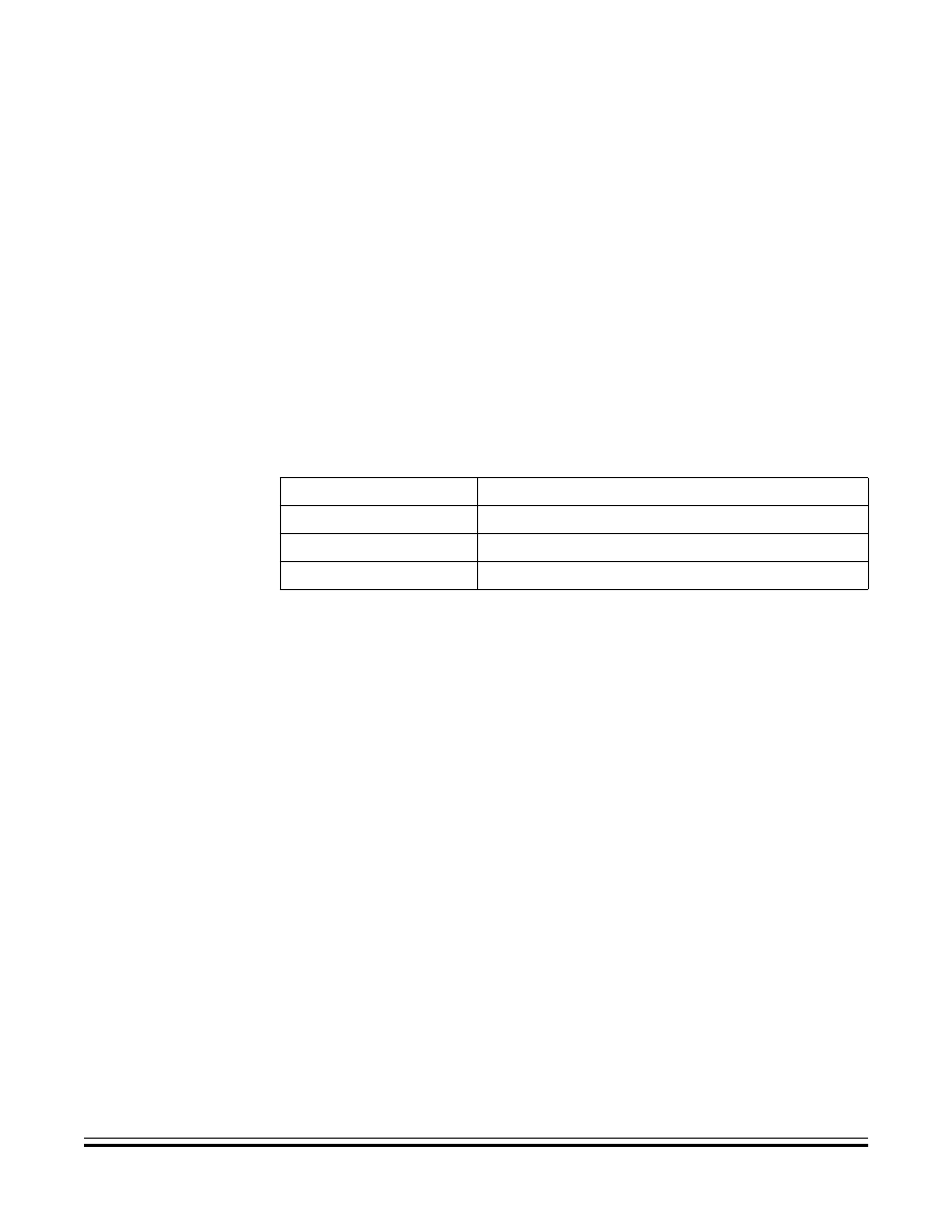
Once the newly downloaded S record programmer starts execution in
the MC68HC11, it configures the SCI to 9600 baud, then waits for a
control character from the PC. This character will determine the
operating mode of the S record programmer. The options available are
shown in
. Note that these programming utilities can be used to
load and verify external RAM as well as external EEPROM.
If the S record programmer has been downloaded successfully, the PC
resident program will now:
1. Request whether the downloaded data must be echoed to the
screen
2. Prompt the user for the required operating mode
3. Request the name of the S record file to be downloaded from
the PC
Once the download starts, every character in the S record file is
immediately echoed back to the PC. This ensures synchronism between
the PC and the MC68HC11, and at the same time it removes some of
the overhead associated with the EEPROM programming delay time. It
also removes the need for a hardware handshake.
Table 3. S Record Downloader Operating Mode Options
Control Character
Operating Mode
X
Program external EEPROM/RAM
I
Program internal EEPROM
V
Verify internal or external EEPROM/RAM

Application Note
AN1010
6
MOTOROLA
Verify Option
If a verify error occurs, the actual stored byte value is returned to the PC,
where it is displayed with a preceding colon delimiter. In this way,
EEPROM data and address faults can be quickly identified by
inspection.
At the end of the verify download, the total number of errors is displayed.
Internal or External Option
If a programming error occurs in either internal or external programming
mode, for instance, if the read back data after programming does not
correspond to the expected data, the MC68HC11-resident software will
hang up. This condition is detected by the PC-resident program, which
will then abort the download and display an error message. This same
error message is displayed if a fault or incorrect connection exists on the
serial link between the PC and MC68HC11.
The one exception to this operation stems from the fact that changes to
the MC68HC11’s CONFIG register can be detected only after a
subsequent hardware reset. If the CONFIG register address ($103F) is
detected, then the CONFIG register is not read directly after
programming. This prevents premature termination of the download.
To allow programming of the CONFIG register in all mask set versions
of the MC68HC11A series and to permit expanded mode operation, the
MCU resident program switches from bootstrap mode to special test
mode by setting the MDA bit (bit 5) in the HPRIO register (address
$103C).
If the user wishes to maintain operation in bootstrap mode (to verify
internal ROM code, for instance), then the BSET HPRIO,X,#MDA
instruction on the eighth line of program code in EEPROGIX.ASC should
be removed and the program reassembled.

Application Note
Programming Internal EEPROM
AN1010
MOTOROLA
7
Programming Internal EEPROM
The techniques for programming internal and external EEPROM are
quite different.
With internal EEPROM, it is first generally necessary to erase the
required byte (erased state is $FF) and follow with a write of data to the
same address.
The internal programming sequence involves accessing the PPROG
register (address $103B) to latch the EEPROM address and data buses
for the duration that the programming voltage is applied. Also, the
programming time delay must be implemented or initiated by software.
In this application, a software timing loop is used, but one of the internal
MC68HC11 timer functions could equally well be used to provide the
time delay.
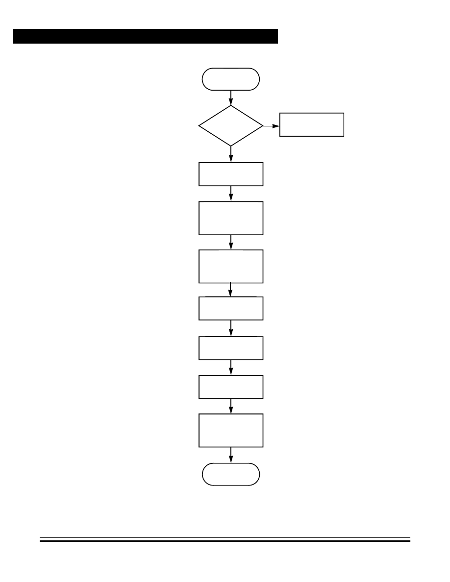
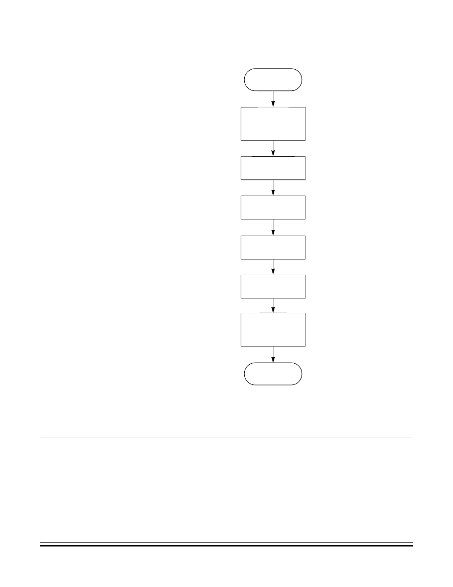
and
show the flowcharts of the internal EEPROM
erase and write sequences.
Application Note
AN1010
8
MOTOROLA
Figure 2. Internal EEPROM Erase Sequence
ENABLE ERASE MODE
ENABLE ADDRESS
AND DATA LATCHES
WRITE TO REQUIRED
MEMORY ADDRESS
(DATA IRRELEVANT)
SELECT BYTE
ERASE MODE
APPLY PROGRAMMING
VOLTAGE
WAIT 10 ms
REMOVE PROGRAMMING
VOLTAGE
DISABLE ERASE MODE
DISABLE ADDRESS
AND DATA LATCHES
END
BEGIN
ERASE CONFIG
REGISTER
?
SELECT BULK
ERASE MODE
Y
N
Application Note
Programming External EEPROM
AN1010
MOTOROLA
9
Figure 3. Internal EEPROM Write Sequence
Programming External EEPROM
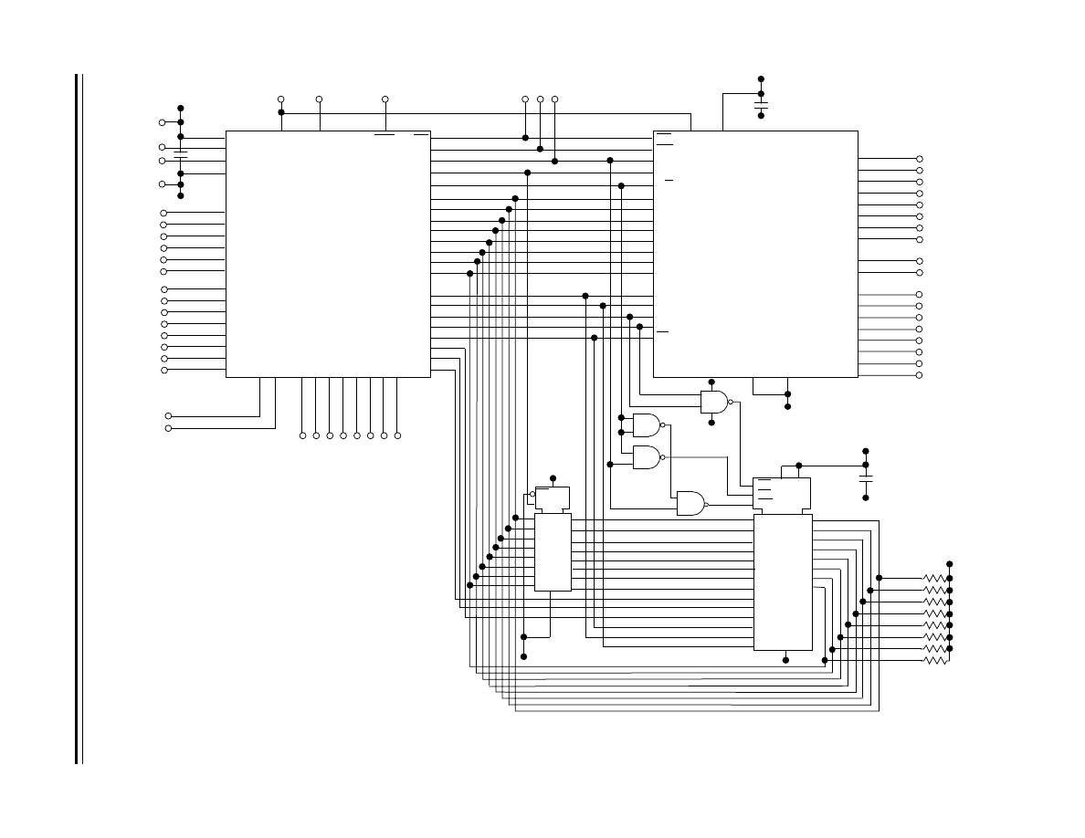
shows the hardware needed to interface the MC68HC11 to an
external 2864 EEPROM, which provides a total of 8 Kbytes of
reprogrammable memory. The addition of the MC68HC24 gives a
minimal component count implementation of a circuit which accurately
emulates the MC68HC11A8 single-chip MCU. The added benefit of
ENABLE BYTE WRITE
ENABLE ADDRESS
AND DATA LATCHES
WRITE REQUIRED DATA
TO REQUIRED ADDRESS
APPLY PROGRAMMING
VOLTAGE
WAIT 10 ms
REMOVE PROGRAMMING
VOLTAGE
DISABLE WRITE MODE
DISABLE ADDRESS
AND DATA LATCHES
END
BEGIN
MODE

Application Note
AN1010
10
MOTOROLA
using the 2864 is that the software designer’s program and/or data can
be modified without removing the emulator from the target system. This
can be particularly useful in applications where the emulator may be
enclosed in a confined space or in an environmental chamber.
To program the 2864 from the PC, the external operating mode option
(X) must be selected from the EELOAD menu.
Programming the 2864 involves fewer operations than are needed for
internal EEPROM, as the former has no equivalent of the PPROG
control register. In addition, the erase sequence and delay time are
handled automatically by the 2864 on-chip logic.
A data polling technique is used to determine the end of the
programming delay time. This involves examining the most significant bit
of the data programmed by reading from the address just written to until
the data becomes true. (During the programming delay time, the MS bit
will read as the complement of the expected data.)
This means that the same software algorithm can be used to download
code or data to external RAM as well as external EEPROM.
Emulator Address Decoding
The emulator circuit in
shows the MC68HC11’s address line
A13 connected to pin 26 of the 2864. Although this pin is actually unused
by the 2864, its inclusion permits the replacement of the 2864 with a
27128 16-Kbyte EEPROM memory.
An important outcome of this is that, when a 2864 is used, the memory
range $C000–$DFFF is mapped over the normally used 8-Kbyte range
of $E000–$FFFF. In practice, this should never pose a problem. When
a 27128 memory is used, its full 16-Kbyte address range of
$C000–$FFFF is available to the MCU.
Included in the S record programmer, irrespective of the selected
programming mode, is a feature to force program execution at the
address specified in the S9 S record address field, provided the address
is not $0000.
AN1010
MOTOROLA
11
Application Note
Emulator Address Decoding
Figure 4. MC68HC11A8 Emulator Using 2864 EEPROM
IRQ
RST
E
STRA
STRB
XIRQ
MODEA
MODEB
19
17
5
4
6
PB4
PB5
PB6
PB7
PB3
PB2
PB1
PB0
PB4
PB5
PB6
PB7
PB3
PB2
PB1
PB0
EXTAL XTAL E0 E1 E2 E3 E4 E5 E6 E7
43 45 47 49 44 46 48 50
PORT E
34
PORT A
33
32
31
30
29
28
27
PORT D
20
21
22
23
24
25
MODE
NC NC NC NC
V
DD
IRQ
RST
E
AS
R/W
AD0
AD1
AD2
AD3
AD4
AD5
AD6
AD7
A12
A13
A14
A15
CS
V
SS
17
43
1 12 23 34
IC1
MC68HC11A1FN
IC2
MC68HC24FN
3
2
18
9 A0/D0
10 A1/D1
11 A2/D2
12 A3/D3
13 A4/D4
14 A5/D5
15 A6/D6
16 A7/D7
38 A12
37 A13
36 A14
35 A15
39 A11
40 A10
41 A9
42 A8
V
DD
V
RL
V
RH
V
SS
26
V
DD
51
V
SS
52
1
C1
0.1 F
PD0
PD1
PD2
PD3
PD4
PD5
PA0
PA1
PA2
PA3
PA4
PA5
PA6
PA7
}
}
}
8
9
10
11
13
14
15
16
PC0
PC1
PC2
PC3
PC4
PC5
PC6
PC7
}
27
26
25
24
22
21
20
19
PB0
PB1
PB2
PB3
PB4
PB5
PB6
PB7
}
7
18
STRA
STRB
PORT C
PORT B
6
5
4
3
44
28
39
41
42
40
38
37
36
35
33
32
31
30
A0
A1
A2
A3
A4
A5
A6
A7
A8
A9
A10
A11
A12
A13
D0
D1
D2
D3
D4
D5
D6
D7
14
R2 10 k
R8 10 k
R7 10 k
R6 10 k
R5 10 k
R4 10 k
R3 10 k
R1 10 k
11
12
13
15
16
17
18
19
V
DD
D0
D1
D2
D3
D4
D5
D6
D7
00
01
02
03
04
05
06
07
CE
CE
WE
V
SS
IC5
2864A
V
SS
1C4
HC373
A0
A1
A2
A3
A4
A5
A6
A7
2
5
6
9
12
15
16
19
3
4
7
8
13
14
17
18
11
1
V
DD
V
SS
12
13
5
4
V
SS
V
SS
2
29
V
DD
14
7
1
2
20
22
27
6
11
9
10
8
IC3-B
10
9
8
7
6
5
4
3
25
24
21
23
2
26
20
1
V
DD
C2
0.1 F
V
DD
IOTEST
3
1C3-A
HC00
IC3-D
HC00
HC00
7
8
IC3-C
HC00
C3
0.1 F
OE
LE
V
SS
V
SS
V
DD
28
10

Application Note
AN1010
12
MOTOROLA
shows the general format of S record files.
Figure 5. S-Record Format
RECORD TYPE: S0, S1, OR S9
S0 — HEADER RECORD: LOAD ADDRESS FIELD = $0000. CODE/DATA FIELD CONTAINS OPTIONAL
DESCRIPTIVE INFORMATION.
S1 — CODE/DATA RECORD. CODE/DATA FIELD CONTAINS EXECUTABLE CODE OR DATA.
S9 — TERMINATION RECORD: LOAD ADDRESS FIELD CONTAINS OPTIONAL EXECUTION ADDRESS.
THERE IS NO CODE/DATA FIELD, JUST A CHECKSUM.
NUMBER OF HEX CHARACTERS FOLLOWING. (Len) = $14
MEMORY LOAD ADDRESS FIELD. (Ldhi, Ldlo) = $C01E
S1
14
C01E0B29BDC02A 18386A3B6F3B391 80926FC39 DE
}
APART FROM THE LETTER S AT THE START, ALL CHARACTERS IN THE RECORDS ARE HEXADECIMAL DIGITS
REPRESENTED IN ASCII FORMAT.
CHECKSUM ALGORITHM: LSB OF
Note: The S record programmer in this application ignores the checksum byte.
[
Len + Ldhi + Ldlo =
∑
byte
k
k = 0
n
]
CHECKSUM BYTE
CODE/DATA FIELD
0 TO N BYTES OF CODE/DATA
10 ’ ******* EELOAD.BAS 20/3/87 Version 1.0 *******/
20 ’ Written by R.Soja, Motorola East Kilbride’
30 ’ Motorola Copyright 1987’
40 ’ This program downloads S record file to the MC68HC11 through special’
50 ’ bootstrap program, designed to program either internal or external’
60 ’ EEPROM in the 68HC11’s memory map’
70 ’ The loader can also verify memory against an S record file.’
80 ’ Downloaded data is optionally echoed on terminal.’
90 ’ ===================================
100 CR$=CHR$(13)
110 MIN$=CHR$(32)
120 MAX$=CHR$(127)
130 ERM$="Can’t find "
140 LOADER$="EEPROGIX.BOO"
150 CLRLN$=SPACE$(80)
160 VER$="1.0": ’Version number of EELOAD’
170 ERRTOT%=0: ’Number of errors found by verify operation’
180 CLS
190 PRINT " <<<<<<<< EELOAD Version ";VER$;" >>>>>>>>"
200 PRINT " <<<<<<<< 68HC11 Internal/External EEPROM loader/verifier >>>>>>>>"
210 PRINT
220 PRINT "==> Before continuing, ensure 68HC11 is in bootstrap mode,"
230 PRINT " RESET is off, and COM1 or COM2 is connected to the SCI"
240 PRINT
250 ’ First make sure loader program is available’
260 ON ERROR GOTO 880
270 OPEN LOADER$ FOR INPUT AS #2

Application Note
Emulator Address Decoding
AN1010
MOTOROLA
13
280 CLOSE #2
290 ON ERROR GOTO 0
300 CHAN$="0"
310 ROW=CSRLIN: ’Store current line number’
320 WHILE CHAN$<>"1" AND CHAN$<>"2"
330 GOSUB 1070
340 LINE INPUT "Enter COM channel number (1/2):",CHAN$
350 WEND
360 CM$="COM"+CHAN$
370 ’ Now set baud rate to 1200 and load EEPROG through boot loader’
380 ’ by executing DOS MODE and COPY commands’
390 SHELL "MODE "+CM$+":1200,N,8,1"
400 SHELL "COPY "+LOADER$+" "+CM$
401 GOSUB 1070
402 FOR 1%=1 to 4:PRINT CLRLN$;:NEXT I%PRINT: ’Clear DOS commands from screen’
410 ECHO$=" "
420 WHILE ECHO$<>"Y" AND ECHO$<>"N"
430 GOSUB 1070
440 LINE INPUT "Do you want echo to screen (Y/N):",ECHO$
450 WEND
470 ROW=CSRLIN: ’Store current line number’
480 EEOPT$=" ": ’Initialise option char’
490 WHILE EEOPT$<>"X" AND EEOPT$<>"I" and EEOPT$<>"V"
500 GOSUB 1070
510 LINE INPUT "Select Internal, eXternal or Verify EEPROM option (I/X/V):",EEOPT$
520 WEND
530 OPT$="Verify"
540 IF EEOPT$="I" THEN OPT$="Internal"
550 IF EEOPT$="X" THEN OPT$="External"
560 ROW=CSRLIN: ’Store current line position in case of file error’
570 RXERR=0: ’Initialise number of RX errors allowed’
580 ON ERROR GOTO 910
590 GOSUB 1070
600 IF OPT$="Verify" THEN INPUT "Enter filename to verify: ",F$ ELSE INPUT "Enter filename to
download:",F$
610 CLOSE
620 OPEN F$ FOR INPUT as #2
630 ON ERROR GOTO 0
640 ’COM1 or 2 connected to SCI on HC11’
650 OPEN CM$+":9600,N,8,1" AS #1
660 ’Establish contact with HC11 by sending CR char & waiting for echo’
670 ON ERROR GOTO 860: ’Clear potential RX error’
680 PRINT #1,CR$;
690 GOSUB 990: ’Read char into B$’
700 ’Transmit Internal,External or Verify EEPROM option char to 68HC11’
710 PRINT #1,EEOPT$;:GOSUB 990: ’No echo to screen’
720 ON ERROR GOTO 930
730 PRINT "Starting download of <";F$;"> to: ";OPT$;" Eeprom"
732 IF ECHO$="Y" THEN E%=1 ELSE E%=0
734 IF EOPT$="V" THEN V%=1 ELSE V%=0
740 WHILE NOT EOF(2)
750 INPUT #2,S$
751 L%=LEN(S$)
752 FOR I%=1 to L%
760 PRINT #1,MID$(S$,I%,1);:GOSUB 990:IF E% THEN PRINT B$;
770 IF V% THEN GOSUB 1030:IF C$<>"" THEN PRINT ":";HEX$(ASC(C$));
785 NEXT I%
787 IF E% THEN PRINT
790 WEND
795 PRINT
800 PRINT "Download Complete"

Application Note
AN1010
14
MOTOROLA
810 IF V% THEN PRINT ERRTOT%;" error(s) found"
820 CLOSE #2
830 SYSTEM
840 END
850 ’ ------------------’
860 IF RXERR>5 THEN 940 ELSE RXERR=RXERR+1:RESUME 610
870 ’ ------------------’
880 PRINT:PRINT ERM$;LOADER$:PRINT "Program aborted"
890 GOTO 830
900 ’-------------------’
910 PRINT ERM$;F$;SPACE$(40)
920 RESUME 580
930 ’-------------------’
940 PRINT:PRINT "Communication breakdown: Download aborted"
950 GOTO 820
960 ’-------------------’
970 ’--SUB waits for received character, with time limit’
980 ’-- returns with char in B$, or aborts if time limit exceeded’
990 T0%=0:WHILE LOC(1)=0:IF T0%>100 THEN 940 ELSE T0%=T0%+1:WEND
1000 B$=INPUT$(1,#1):RETURN
1010 ’-------------------’
1020 ’--SUB waits for received character, with time limit’
1025 ’-- returns with char in C$, or null in C$ if time limit exceeded’
1030 T0%=0:C$="":WHILE LOC(1)=0 AND T0%<1:T0%=T0%+1:WEND
1040 IF LOC(1)>0 THEN C$=INPUT$(1,#1):ERRTOT%=ERRTOT%+1
1050 RETURN
1060 ’-------------------’
1070 ’--SUB Clear line ’
1080 LOCATE ROW,1,1:PRINT CLRLN$
1090 LOCATE ROW,1,1:RETURN
1100 ’-------------------’
1 A
************************************************************************************************************************
2 A
* EEPROGIX.ASC 19/3/87 Revision 1.0
3 A
*
*
4 A
* Written by R.Soja, Motorola, East Kilbride
*
5 A
* Motorola Copyright 1987.
*
6 A
*
*
7 A
* This program loads S records from the host to
*
8 A
* either a 2864 external EEPROM on the 68HC11 external bus,
*
9 A
* or to the 68HC11’s internal EEPROM. It can also be used
*
10 A
* verify memory contents against an S record file or just
*
11 A
* load RAM located on the 68HC11’s external bus.
*
12 A
* Each byte loaded is echoed back to the host.
*
13 A
* When programming a 2864, data polling is used to detect
*
14 A
* completion of the programming cycle.
*
15 A
* As the host software always waits for the echo before
*
16 A
* downloading the next byte, host transmission is suspended
*
17 A
* during the data polling period.
*
18 A
* Because the serial communication rate (~1mS/byte) is
*
19 A
* slower than the 2864 internal timer timeout rate (~300
µ
s)
*
20 A
* page write mode cannot be used. This means that data
*
21 A
* polling is active on each byte written to the EEPROM,
*
22 A
* after an initial delay of approx 500
µ
s.
*
23 A
*
*
24 A
* When the internal EEPROM is programmed, instead of data
*
25 A
* polling, each byte is verified after programming.
*
26 A
* In this case, the 500
µ
s delay is not required and is
*
27 A
* bypassed.
*
28 A
* If a failure occurs, the program effectively hangs up. It
*
29 A
* is the responsibility of the host downloader program to
*
30 A
* detect this condition and take remedial action.
*

Application Note
Emulator Address Decoding
AN1010
MOTOROLA
15
31 A
* The BASIC program EELOAD just displays a ’Communication
*
32 A
* breakdown’ message, and terminates the program.
*
33 A
*
*
34 A
* When used in the verify mode, apart from the normal echo
*
35 A
* back of each character, all differences between memory
*
36 A
* and S record data are also sent back to the host.
*
37 A
* The host software must be capable of detecting this, and
*
38 A
* perform the action required.
*
39 A
* The BASIC loader program EELOAD simply displays the
*
40 A
* returned erroneous byte adjacent to the expected byte,
*
41 A
* separated by a colon.
*
42 A
*
*
43 A
* Before receiving the S records, a code byte is received
*
44 A
* from the host. i.e.:
*
45 A
ASCII ’X’ for external EEPROM
*
46 A
ASCII ’I’ for internal EEPROM
*
47 A
ASCII ’V’ for verify EEPROM
*
48 A
*
*
49 A
* This program is designed to be used with the BASIC EELOAD
*
50 A
* program.
*
51 A
* Data transfer is through the SCI, configured for 8 data
*
52 A
* bits, 9600 baud.
*
53 A
*
*
54 A
PAGE
55 A
* Constants
56 A 0080
TDRE
EQU
$80
57 A 0020
RDRF
EQU
$20
58 A 0020
MDA
EQU
$20
59 A 0040
SMOD
EQU
$40
60 A 0D05
ms10
EQU
10000/3 10ms delay with 8MHz xtal.
61 A 00A6
us500
EQU
500/3 500us delay.
62 A
*
63 A
* Registers
64 A 002B
BAUD
EQU
$2B
65 A 002C
SCCR1
EQU
$2C
66 A 002D
SCCR2
EQU
$2D
67 A 002E
SCSR
EQU
$2E
68 A 002F
SCDR
EQU
$2F
69 A 003B
PPROG
EQU
$3B
70 A 003C
HPRIO
EQU
$3C
71 A 103F
CONFIG
EQU
$103F
72 A
*
73 A
* Variables. Note: They overwrite initialisation code!!!!
74 A 0000
ORG
$0
75 P 0000 0001
EEOPT
RMB
1
76 P 0001 0001
MASK
RMB
1
77 P 0002 0001
TEMP
RMB
1
78 P 0003 0001
LASTBYTE
RMB
1
79 A
*
80 A
* Program
81 A 0000
ORG
$0
82 A 0000 8E00FF
LDS
#$FF
83 A 0003 CE1000
LDX
#$1000
Offset for control registers.
84 A 0006 6F2C
CLR
SCCR1,X
Initialise SCI for 8 data bits, 9600 baud
85 A 0008 CC300C
LDD
#$300C
86 A 000B A72B
STAA
BAUD,X
87 A 000D E72D
STAB
SCCR2,X
88 A 000F 1C3C20
BSET
HPRIO,X,#MDA
Force Special Test mode first,
89 A
*=>> MAINTAIN SPECIAL TEST MODE TO ALLOW B96D CONFIG REGISTER PROGRAMMING <<==
90 A
*
BCLR HPRIO,X,#SMOD and then expanded mode. (From Bootstrap mode)

Application Note
AN1010
16
MOTOROLA
91 A 0012 9F00
ReadOpt
STS
<EEOPT
Default to internal EEPROM: EEOPT=0;
MASK=$FF;
92 A 0014 8D7C
BSR
READC
Then check control byte for external or
93 A 0016 C149
CMPB
#’I’
internal EEPROM selection.
94 A 0018 2714
BEQ
LOAD
95 A 001A C158
CMPB
#’X’
If external EEPROM requested
96 A 001C 2609
BNE
OptVerf
97 A 001E 7C0000
INC
EEOPT
then change option to 1
98 A 0021 8680
LDAA
#$80
99 A 0023 9701
STAA
<MASK
and select mask for data polling mode.
100 A 0025 2007
BRA
LOAD
101 A
*
102 A 0027 C156
OptVerf
CMPB
#’V’
If not verify then
103 A 0029 26E7
BNE
ReadOpt
get next character else
104 A 002B 7A0000
DEC
EEOPT
make EEOPT flag negative.
105 A
*
106 A 002E
LOAD
EQU
*
107 A 002E 8D62
BSR
READC
108 A 0030 C153
CMPB
#’S
Wait until S1 or S9 received,
109 A 0032 26FA
BNE
LOAD
discarding checksum of previous S1
record.
110 A 0034 8D5C
BSR
READC
111 A 0036 C131
CMPB
#’1
112 A 0038 2719
BEQ
LOAD1
113 A 003A C139
CMPB
#’9
114 A 003C 26F0
BNE
LOAD
115 A 003E 8D5F
BSR
RDBYTE
Complete reading S9 record before
terminating
116 A 0040 17
TBA
117 A 0041 8002
SUBA
#2
# of bytes to read including checksum.
118 A 0043 8D6B
BSR
GETAD
Get execution address in Y
119 A 0045 8D58
LOAD9
BSR
RDBYTE
Now discard remaining bytes,
120 A 0047 4A
DECA
including checksum.
121 A 0048 26FB
BNE
LOAD9
122 A 004A 188C0000
CPY
#0
If execution address =0 then
123 A 004E 27FE
BEQ
*
hang up else
124 A 0050 186E00
JMP
,Y
jump to it!
125 A
*
126 A 0053
LOAD1
EQU
*
127 A 0053 8D4A
BSR
RDBYTE
Read byte count of S1 record into ACCB
128 A 0055 17
TBA
and store in ACCA
129 A 0056 8003
SUBA
#3
Remove load address & checksum bytes
from count
130 A 0058 8D56
BSR
GETADR
Get load address into X register.
131 A 005A 1809
DEY
Adjust it for first time thru’ LOAD2
loop.
132 A 005C 2017
BRA
LOAD1B
133 A
*
134 A 005E D600
LOAD1A
LDAB
EEOPT
Update CC register
135 A 0060 2B25
BMI
VERIFY
If not verifying EEPROM then
136 A 0062 2705
BEQ
DATAPOLL
If programming external EEPROM
137 A 0064 C6A6
LDAB
#us500
138 A 0066 5A
WAIT1
DECB
then wait 500us max.
139 A 0067 26FD
BNE
WAIT1
140 A 0069 18E600
DATAPOLL
LDAB
,Y
Now either wait for completion of
programming
141 A 006C D803
EORB
<LASTBYTE
programming cycle by testing MS bit of
last data written to
142 A 006E D401
ANDB
<MASK
last data written to memory or just
143 A 0070 26F7
BNE
DATAPOLL
verify internal programmed data.

Application Note
Emulator Address Decoding
AN1010
MOTOROLA
17
144 A 0072 4A
LOAD1E
DECA
When all bytes done,
145 A 0073 27B9
BEQ
LOAD
get next S record (discarding checksum)
146 A 0075 8D28
LOAD1B
BSR
RDBYTE
else read next data byte into ACCB.
147 A 0077 1808
INY
Advance to next load address
148 A 0079 7D0000
TST
EEOPT
149 A 007C 2B05
BMI
LOAD1D
If verifying, then don’t program byte!
150 A 007E 2743
BEQ
PROG
If internal EEPROM option selected then
program
151 A 0080 18E700
STAB
,Y
else just store byte at address.
152 A 0083 D703
LOAD1D
STAB
<LASTBYTE
Save it for DATA POLLING operation.
153 A 0085 20D7
BRA
LOAD1A
154 A
*
155 A 0087 18E600
VERIFY
LDAB
,Y
If programmed byte
156 A 008A D103
CMP8
<LASTBYTE
is correct then
157 A 008C 27E4
BEQ
LOAD1E
read next byte
158 A 008E 8D08
BSR
WRITEC
else send bad byte back to host
159 A 0090 20E0
BRA
LOAD1E
before reading next byte.
160 A
*
161 A 0092
READC
EQU
*
ACCA, X, Y regs unchanged by this
routine.
162 A 0092 1F2E20FC
BRCLR
SCSR,X,#RDRF,*
163 A 0096 E62F
LDAB
SCDR,X
Read next char
164 A 0098 1F2E80FC
WRITEC
BRCLR
SCSR,X,#TDRE,*
165 A 009C E72F
STAB
SCDR,X
and echo it back to host.
166 A 009E 39
RTS
Return with char in ACCB.
167 A
*
168 A 009F 8DF1
RDBYTE
BSR
READAC
1st read MS nibble
169 A 00A1 8D17
BSR
HEXBIN
Convert to binary
170 A 00A3 58
LSLB
and move to upper nibble
171 A 00A4 58
LSLB
172 A 00A5 58
LSLB
173 A 00A6 58
LSLB
174 A 00A7 D702
STAB
<TEMP
175 A 00A9 8DE7
BSR
READC
Get ASCII char in ACCB
176 A 00AB 8D0D
BSR
HEXBIN
177 A 00AD DA02
ORAB
<TEMP
178 A 00AF 39
RTS
Return with byte in ACCB
179 A
*
180 A 00B0
GETADR
EQU
*
181 A 00B0 36
PSHA
Save byte counter
182 A 00B1 8DEC
BSR
RDBYTE
Read MS byte of address
183 A 00B3 17
TBA
and put it in MS byte of ACCD
184 A 00B4 8DE9
BSR
RDBYTE
Now read LS byte of address into LS byte
of ACCD
185 A 00B6 188F
XGDY
Put load address in Y
186 A 00B8 32
PULA
Restore byte counter
187 A 00B9 39
RTS
and return.
188 A
*
189 A 00BA
HEXBIN
EQU
*
190 A 00BA C139
CMP8
#’9
If ACCB>9 then assume its A-F
191 A 00BC 2302
BLS
HEXNUM
192 A 00BE CB09
ADDB
#9
193 A 00C0 C40F
HEXNUM
ANDB
#$F
194 A 00C2 39
RTS
195 A
*
196 A 00C3
PROG
EQU
*
197 A 00C3 36
PSHA
Save ACCA.
198 A 00C4 8616
LDAA
#$16
Default to byte erase mode
199 A 00C6 188C103F
CPY
#CONFIG
If byte’s address is CONFIG then use
200 A 00CA 2602
BNE
PROGA

Application Note
AN1010
18
MOTOROLA
201 A 00CC 8606
LDAA
#$06
bulk erase, to allow for A1 &A8 as well
as A2.
202 A 00CE 8D10
PROGA
BSR
PROGRAM
Now byte erase or entire memory + CONFIG.
203 A 00D0 8602
LDAA
#2
204 A 00D2 8D0C
BSR
PROGRAM
Now program byte.
205 A 00D4 188C103F
CPY
#CONFIG
If byte was CONFIG register then
206 A 00D8 2603
BNE
PROGX
207 A 00DA 18E600
LDAB
,Y
Load ACCB with old value, to prevent
hangup later.
208 A 00DD 32
PROGX
PULA
Restore ACCA
209 A 00DE 20A3
BRA
LOAD1D
and return to main bit.
210 A
*
211 A 00E0
PROGRAM
EQU
*
212 A 00E0 A73B
STAA
PPROG,X
Enable internal addr/data latches.
213 A 00E2 18E700
STAB
,Y
Write to required address
214 A 00E5 6C3B
INC
PPROG,X
Enable internal programming voltage
215 A 00E7 3C
PSHX
216 A 00E8 CE0D05
LDX
#mS10
and wait 10mS
217 A 00EB 09
WAIT2
DEX
218 A 00EC 26FD
BNE
WAIT2
219 A 00EE 38
PULX
220 A 00EF 6A3B
DEC
PPROG,X
Disable internal programming voltage
221 A 00F1 6F3B
CLR
PPROG,X
Release internal addr/data latches
222 A 00F3 39
RTS
and return
223 A
*
224 A
END
SYMBOL TABLE: Total Entries= 41
BAUD
002B
PROGA
00CE
CONFIG
103F
PROGRAM
00E0
DATAPOLL
0069
PROGX
00DD
EEOPT
0000
RDBYTE
009F
GETADR
00B0
RDRF
0020
HEXBIN
00BA
READC
0092
HEXNUM
00C0
ReadOpt
0012
HPRIO
003C
SCCR1
002C
LASTBYTE
0003
SCCR2
002D
LOAD
002E
SCDR
002F
LOAD1
0053
SCSR
002E
LOAD1A
005E
SMOD
0040
LOAD1B
0075
TDRE
0080
LOAD1D
0083
TEMP
0002
LOAD1E
0072
VERIFY
0087
LOAD9
0045
WAIT1
0066
MASK
0001
WAIT2
00EB
MDA
0020
WRITEC
0098
OptVerf
0027
mS10
0D05
PPROG
003B
uS500
00A6
PROG
003C

Application Note
Emulator Address Decoding
AN1010
MOTOROLA
19

NON-DISCLOSURE AGREEMENT REQUIRED
Application Note
AN1010/D
© Motorola, Inc. 1988, 2000
Motorola reserves the right to make changes without further notice to any products herein. Motorola makes no warranty, representation or guarantee regarding the suitability of its
products for any particular purpose, nor does Motorola assume any liability arising out of the application or use of any product or circuit, and specifically disclaims any and all liability,
including without limitation consequential or incidental damages. "Typical" parameters which may be provided in Motorola data sheets and/or specifications can and do vary in different
applications and actual performance may vary over time. All operating parameters, including "Typicals" must be validated for each customer application by customer's technical experts.
Motorola does not convey any license under its patent rights nor the rights of others. Motorola products are not designed, intended, or authorized for use as components in systems
intended for surgical implant into the body, or other applications intended to support or sustain life, or for any other application in which the failure of the Motorola product could create a
situation where personal injury or death may occur. Should Buyer purchase or use Motorola products for any such unintended or unauthorized application, Buyer shall indemnify and hold
Motorola and its officers, employees, subsidiaries, affiliates, and distributors harmless against all claims, costs, damages, and expenses, and reasonable attorney fees arising out of,
directly or indirectly, any claim of personal injury or death associated with such unintended or unauthorized use, even if such claim alleges that Motorola was negligent regarding the
design or manufacture of the part. Motorola and
are registered trademarks of Motorola, Inc. Motorola, Inc. is an Equal Opportunity/Affirmative Action Employer.
How to reach us:
USA/EUROPE/Locations Not Listed: Motorola Literature Distribution; P.O. Box 5405, Denver, Colorado 80217. 1-303-675-2140 or 1-800-441-2447
JAPAN: Motorola Japan Ltd.; SPS, Technical Information Center, 3-20-1, Minami-Azabu, Minato-ku, Tokyo 106-8573 Japan. 81-3-3440-3569
ASIA/PACIFIC: Motorola Semiconductors H.K. Ltd.; Silicon Harbour Centre, 2 Dai King Street, Tai Po Industrial Estate, Tai Po, N.T., Hong Kong.
852-26668334
Technical Information Center: 1-800-521-6274
HOME PAGE: http://www.motorola.com/semiconductors/
Document Outline
- Introduction
- Verify Option
- Internal or External Option
- Programming Internal EEPROM
- Programming External EEPROM
- Emulator Address Decoding
Wyszukiwarka
Podobne podstrony:
MC68HC705V8 MC68HC705V8 EEPROM Programming Tool ODESSA
EEPROM PROGRAMMIERUNG
Programator szeregowych pamięci EEPROM 93C46
Charakterystyka programu
1 treści programoweid 8801 ppt
Programowanie rehabilitacji 2
Rola rynku i instytucji finansowych INowy Prezentacja programu Microsoft PowerPoint
Nowy Prezentacja programu Microsoft PowerPoint ppt
więcej podobnych podstron