[
Microcontrollers & Embedded
•
Analogue
•
Audio
•
Digital
•
Test &
Measurement
]
www.elektor.com
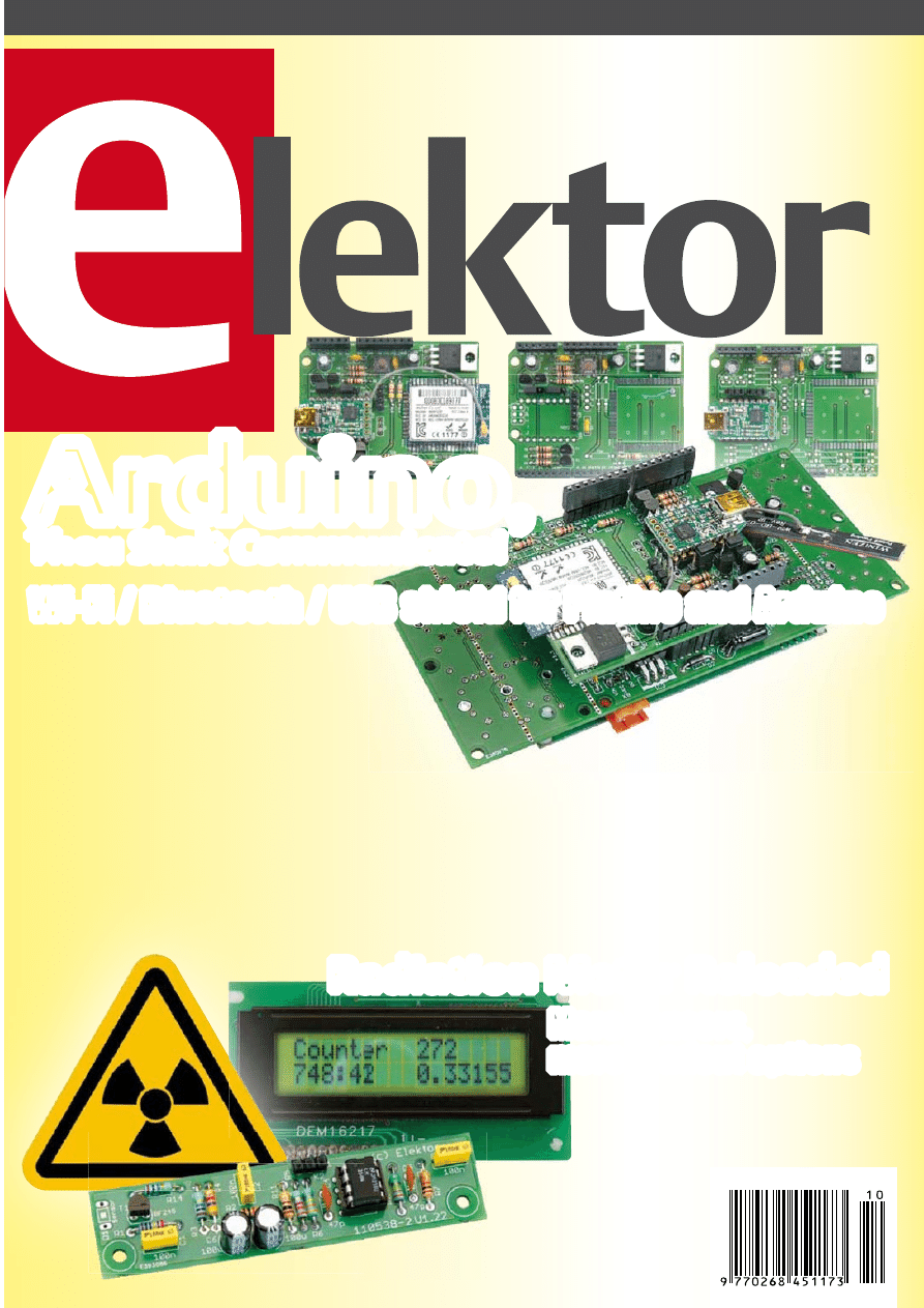
Wi-Fi / Bluetooth / USB shield for Platino and Arduino
More sensors,
more readout options
Thou Shalt Communicate!
Radiation Meter Reloaded
USB Isolator
Avoid interference and earth loops
Vocal Annunciator
How about making your next project speak?
Intelligent PC Fan Controller
Control, monitor & configure a maximum of six PWM fans
✚
✚
✚
Arduino
,
October 2012 AUS$ 14.90 - NZ$ 17.90 - SAR 105.95 - NOK 102 £ 4.90
2 29
www.pcb-pool.com
www.beta-eSTORE.com
FREE Stencil
with every PCB Prototype order
Develop, assemble, solder
Large Beta-Reflow-Kit
€
129
,
00
*
Reflow-Controller
€
129
,
00
*
€
6,
00
*
Arduino Mega (ATMega 1280-16AU)
compatible
€
36
,
50
*
LED Blinker 6 LEDs
* Incl. V
AT and e
xclusiv
e of shipping costs
Discount
Evaluate 5 orders and
get 10% off
€
279
,
00
UHF RFID Starterkit
Basic
PCB-POOL® is a r
egister
ed tr
ademark of Beta LA
YOUT GmbH
Free Phone UK: 0800 389 8560
sales@pcb-pool.com
PCB Prototypes
and small series
4
10-2012 elektor
Looking forward to being
inundated (again)
Here at Elektor we get the numbers all
wrong occasionally. Although we’re
perfectly able to calculate, say, bit time
offsets to less than a microsecond using C,
or Johnson noise levels in an NE553 opamp,
we were horribly wrong with our guess-
timate of the interest in our Embedded
Linux article series. But happy to be wide
off the mark! Let me explain.
On Friday August 17, while working from
my home on a new book called LabworX
2: Mastering Surface Mount Technology,
I wanted to correct a small bit of text
somewhere on the elektor.com website
using my administrator rights. Now I have
a pretty slow PC at home, but this time the
backoffice login procedure seemed to take
so long I decided to do a small inspec-
tion round of my garden. On returning to
my desk, I was greeted by error message
–392a on the screen basically saying some-
thing was overloaded. Then the telephone
rang (it hardly ever does that) and our
editorial secretary told me to sort-of-
instantly write and email a short message
telling customers that our webserver had
been on 404 due to a flood of requests for
an archive file that belongs with our recent
Embedded Linux series.
The problem was fixed almost instantly
by moving the archive file to another area
with capacity to spare. Apologies to all of
you Linux fans and all other Elektor readers
seeing 404s and having to wait a while
for the file to become available. We have
adapted the kernel (read all about it in
this edition!), and fitted a pressure release
valve on our webserver.
Happy reading,
Jan Buiting, Managing Editor
6
Colophon
Who’s who at Elektor.
8
News & New Products
A monthly roundup of all the latest in
electronics land.
14 USB Isolator
This little circuit provides electrical
isolation of data lines and supply lines
between the PC and the USB device.
18 Embedded Linux made Easy (4)
This month we delve deep into the
various commands and options offered by
the kernel.
28 Thou Shalt Communicate!
Here’s a Platino and Arduino compatible
shield that packs Wi-Fi, Bluetooth and
USB on a single board.
34 AVR Software Defined Radio (6)
In this instalment we discuss the time
encoding format applied on the BBC
Droitwich transmitter on 198 kHz.
40 Picoammeter
This little instrument was designed to
cover those infinitesimally small currents
between 0.1 pico-ampere to 1 micro-
ampere.
43 E-Labs Inside:
- Shifting RS485 Grounds
- AVR reset-out-of-the-blue issue
- E-pollution!
- Your all-time favourite component
46 Energy Harvesting
with the LTC3108 & LTC3588-1
Raymond’s pick of the month in terms of
components
5
elektor 10-2012
48 Arduino on Course (2)
No matter where your sensors are on the
globe, you will be able to read them using
Arduino functionality extended with GSM
/ GPRS.
54 Radiation Meter Reloaded
Elektor’s simple radiation meter keeps
evolving, both at the front end (the
sensors) and the user end (enter the PC!)
60 Electronics for Starters (8)
This series has met with great popularity
with young & old. This month we tackle
the basics of audio amplification.
64 Vocal Annunciator
Wouldn’t it be great to have a
measurement system read out values
aloud? Here’s how.
68 Intelligent PC Fan Controller
This circuit allows six (PC) fans to be
controlled, configured and monitored
with a good deal of intelligence.
76 Retronics: Marconi Instruments
TF801D/1 AM RF Signal Generator.
An RF signal generator built like rock and
still working great after 50 years. Series
Editor: Jan Buiting
78 Hexadoku
Elektor’s monthly puzzle with an
electronics touch.
84 Coming Attractions
Next month in Elektor magazine.
CONTENTS
Volume 38
October 2012
no. 430
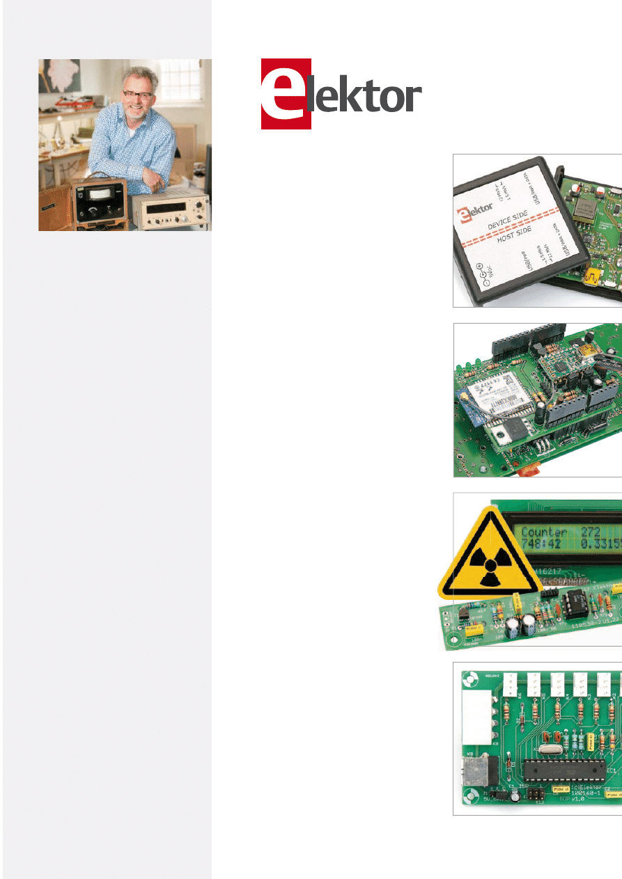
14 USB Isolator
If your USB device ever suffers from noise caused by an earth loop or if you want
to protect your PC against external voltages then you need a USB isolator. The
circuit described here offers an optimal electrical isolation of the data lines as
well as the supply lines between the PC and the USB device.
68 Intelligent PC Fan Controller
With the help of the circuit described here you can actively control up to six
fans, while the temperature can be measured in various places inside the PC
case using a number of sensors. A PC program is used to configure and monitor
the fans, which communicates with the fan control board via a USB link.
54 Radiation Meter Reloaded
Elektor’s Simple Radiation Meter is currently being used by many readers,
mainly in making long-term measurements and in investigating weakly radio-
active samples. There are several ways in which we can modify and improve the
design, and we look here at a few examples.
28 Thou Shalt Communicate!
You may have a Facebook account, but what about your oscilloscope? Does
your multimeter tweet enough? Is your soldering iron linked in? You may be
a non-communicative nerd but your bench power supply may be craving for
social interaction. With the add-on board described in this article you can hook
up anything to everything, with or without wires.
Our international teams
6
10-2012 elektor
elektor
The Network
The Team
Managing Editor:
Jan Buiting
(editor@elektor.com)
International Editorial Staff:
Harry Baggen, Thijs Beckers, Eduardo Corral, Wisse Hettinga, Denis Meyer, Jens Nickel, Clemens Valens
Design staff:
Thijs Beckers, Ton Giesberts, Luc Lemmens, Raymond Vermeulen, Jan Visser
Membership Manager:
Raoul Morreau
Graphic Design & Prepress:
Giel Dols, Mart Schroijen
Online Manager:
Daniëlle Mertens
Managing Director:
Don Akkermans
Volume 38, Number 430, October 2012 ISSN 1757-0875
Publishers:
Elektor International Media,
78 York Street, London W1H 1DP, United Kingdom.
Tel. +44 (0)20 7692 8344
www.elektor.com
the magazine is available from newsagents, bookshops and
electronics retail outlets, or on subscription.
elektor is published 11 times a year with a double issue for July & August.
Subscriptions:
Elektor International Media,
78 York Street, London W1H 1DP, United Kingdom.
Tel. +44 (0)20 7692 8344 , fax: +31 (0)46 43 70 161
Internet: www.elektor.com/subs
Email: subscriptions@elektor.com
Rates and terms are given on the Subscription Order Form.
Head Office:
Elektor International Media b.v.
P.O. Box 11 NL-6114-ZG Susteren The Netherlands.
Telephone: +31 (0)46 4389444, Fax: (+31) 46 4370161
Distribution:
Seymour, 2 East Poultry Street, London EC1A, England.
Telephone:+44 (0)20 7429 4073
UK Advertising:
Elektor International Media b.v.
P.O. Box 11 NL-6114-ZG Susteren The Netherlands.
Tech the Future explores the solutions for a
sustainable future provided by technology,
creativity and science.
United Kingdom
Wisse Hettinga
+31 (0)46 4389428
w.hettinga@elektor.com
USA
Hugo Vanhaecke
+1 860-875-2199
h.vanhaecke@elektor.com
Germany
Ferdinand te Walvaart
+31 46 4389417
f.tewalvaart@elektor.de
France
Denis Meyer
+31 46 4389435
d.meyer@elektor.fr
Netherlands
Harry Baggen
+31 46 4389429
h.baggen@elektor.nl
Spain
eduardo Corral
+34 91 101 93 95
e.corral@elektor.es
Italy
Maurizio del Corso
+39 2.66504755
m.delcorso@inware.it
Sweden
Wisse Hettinga
+31 46 4389428
w.hettinga@elektor.com
Brazil
João Martins
+55 11 4195 0363
joao.martins@editorialbolina.com
Portugal
João Martins
+351 21413-1600
joao.martins@editorialbolina.com
India
Sunil D. Malekar
+91 9833168815
ts@elektor.in
Russia
Nataliya Melnikova
+7 (965) 395 33 36
elektor.russia@gmail.com
Turkey
Zeynep köksal
+90 532 277 48 26
zkoksal@beti.com.tr
South Africa
Johan Dijk
+27 78 2330 694 / +31 6 109 31 926
j.dijk @elektor.com
China
Cees Baay
+86 21 6445 2811
CeesBaay@gmail.com

Membership Counter
Supporting Companies
AudioXpress
www.audioamateur.com . . . . . . . . . . . . . . . . 59
Beta Layout
www.pcb-pool.com . . . . . . . . . . . . . . . . . . . . 2
CES
www.cesweb.org . . . . . . . . . . . . . . . . . . . . . 47
Eurocircuits
www.elektorpcbservice.com . . . . . . . . . . . . . . 42
EzPCB
www.siliconray.com . . . . . . . . . . . . . . . . . . . 27
Jackaltac
www.jackaltac.com . . . . . . . . . . . . . . . . . . . . 9
Labcenter
www.labcenter.com . . . . . . . . . . . . . . . . . . . 88
MikroElektronika
www.mikroe.com. . . . . . . . . . . . . . . . . . . . . . 3
National Instruments
www.ni.com/daq . . . . . . . . . . . . . . . . . . . . . 13
Pico Technology
www.picotech.com/CM124 . . . . . . . . . . . . . . . 41
Reichelt
www.reichelt.co.uk . . . . . . . . . . . . . . . . . . . . 11
7
elektor 10-2012
elektor
Not a supporting company yet?
Contact Johan Dijk (j.dijk@elektor.com, +31 6 109 31 926) to reserve your own space for the next edition of our members' magazine
Not a member yet?
Sign up at www.elektor.com/member
Telephone: +31 (0)46 43 89 444, Fax: +31 (0)46 43 70 161
Email: j.dijk@elektor.com
Internet: www.elektor.com
Advertising rates and terms available on request.
Copyright Notice
the circuits described in this magazine are for domestic use
only. All drawings, photographs, printed circuit board layouts,
programmed integrated circuits, disks, CD-roMs, software
carriers and article texts published in our books and magazines
(other than third-party advertisements) are copyright elektor
International Media b.v. and may not be reproduced or transmit-
ted in any form or by any means, including photocopying, scan-
ning and recording, in whole or in part without prior written per-
mission from the Publisher. Such written permission must also be
obtained before any part of this publication is stored in a retrieval
system of any nature. Patent protection may exist in respect of
circuits, devices, components etc. described in this magazine.
the Publisher does not accept responsibility for failing to identify
such patent(s) or other protection. the submission of designs or
articles implies permission to the Publisher to alter the text and
design, and to use the contents in other elektor International
Media publications and activities. the Publishers cannot guaran-
tee to return any material submitted to them.
Disclaimer
Prices and descriptions of publication-related items subject to
change. errors and omissions excluded.
© Elektor International Media b.v. 2012
Printed in the Netherlands
We
now have
members
in
countries.
• The latest on electronics and
information technology
• Hints, tips and interesting offers
• In your own mailbox each Friday
Take out a FREE
membership to
Elektor Weekly
S
83
274932
8
10-2012 elektor
NEWS & NEW PRODUCTS
New digital advanced bus converter lowers power
consumption
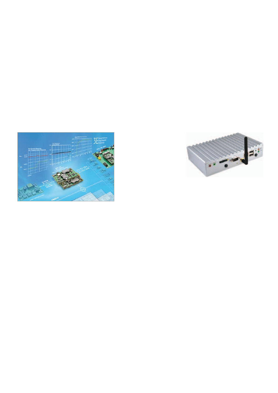
Ericsson has unveiled the first model in its second generation of digital Advanced Bus Con-
verter (ABC) products. Based upon the FRIDA II platform, which was announced earlier this
year, the Ericsson BMR456 3E Advanced Bus Converter delivers unprecedented performance
to system architects who are developing equipment for ICT (Information and Communica-
tion Technology) applications that require fast response time, tightly regulated intermedi-
ate bus voltages and high efficiency at any point of operation to reduce power consumption.
This new generation of fully regulated digital DC/DC converters is based on a 32-bit ARM
microcontroller that embeds the family’s most advanced firmware to date. The FRIDA II
firmware has been developed by Ericsson to guarantee the highest possible performance
at any point of operation from low load to high load, and to handle line transients, such as
those occurring in ATCA (Advanced Telecommunications Computing Architecture) applica-
tions when, for example, switching from Feed A to Feed B.
Designed to power telecom
and datacom applications, the
BRM456 is available in two
input voltages ranges: 36 V to
75 V, delivering output power of
420 W; and 40 V to 60 V, deliver-
ing output power up to 468 W.
Output voltage can be adjusted
across a range from 4.0 V to
13.2 V via PMBus commands,
making the BMR456 suitable
for Dynamic Bus Voltage opera-
tion resulting in the reduction of
energy consumption when com-
munication data traffic is low.
In addition, taking full advantage of a highly optimized layout and firmware-optimized
parameter switching to reduce power losses, the BMR456 delivers a typical efficiency of
96.5% and exhibits flat curve behavior from 14% to 100% load, positioning the product
as the most efficient Advanced Bus Converter in its category. Designed for flexibility and
high-power applications, when connected in parallel, the Droop Load Sharing (DLS) ver-
sion of the BMR456 telecom (36-75 V) and datacom (40–60 V) versions can deliver 756 W
and 842 W, respectively.
The BMR456 implements the FRIDA II firmware, called the ‘Ericsson DC/DC Energy Opti-
mizer’, which combines advanced Ericsson Intellectual Property (IP) together with a series
of industry-first functionalities to continually optimize switching parameters and reduce
energy consumption to an absolute minimum. The firmware is not just limited to energy
management, but includes an enviable number of features including the ability to han-
dle input voltage transients with slew-rates of up to 0.5 V/µs, while keeping the output
voltage within ±10% and ensuring that the output voltage does not trigger over-voltage
protection. It also offers the highly efficient management of pre-bias start-up operation
and a fully controlled shutdown process, avoiding voltage spikes that could cause an
avalanche condition in the secondary-side synchronous rectification MOSFET, thereby
contributing to improved reliability.
The BMR456 meets the insulation requirements of EN60950, sustains an I/O isolation volt-
age of 2250 VDC, and also offers an extensive set of capabilities and features such as: remote
sensing; PMBus-configurable protection (over-temperature, over-current and over-voltage);
configurable start/stop; precision delay ramp-up; voltage margining; configurable fault
response; power good; and extensive power management programmability.
The BRM456 is fully backward compatible with Ericsson’s previous generation of Advanced
Bus Converters. The device’s I/O connector has been designed to guarantee full alignment
and co-planarity using different soldering processes for both through-hole and surface-
mount assembly. In addition to the mechanical benefits, the Ericsson Advanced Bus Con-
verter footprint offers the necessary flexibility for further board design evolution and the
addition of new features currently under evaluation within the ICT industry.
www.ericsson.com/powermodules - (120487-IX)
JTAG development system
using WiFi
The Debug Store is proud to announce
the availability of the Macraigor Systems
WiFiDemon in Europe. Priced at just £1475,
the WiFiDemon is in stock and ready to ship.
The WiFiDemon is Macraigor’s fastest and
most versatile OCD interface device for use
in the design, debugging and programming
of microprocessor and microcontroller
based embedded systems.
The WiFiDemon can be connected to the
host PC via a 10/100 BaseT Ethernet or WiFi
connection allowing the developer to con-
trol the debugging operation some distance
from his desk — in fact he can be located
across the globe! The WiFiDemon supports
configurable JTAG/BDM clock rates from
4.5 kHz to 24 MHz, allowing very fast code
download and responsive debugging.
The WiFiDemon is fitted with a 40 GB hard
drive, two USB ports (to connect a mouse
and keyboard) and a VGA port to connect a
monitor. The development tools pre-loaded
onto the hard drive can be run on the system
allowing development work to be carried out
locally — this makes it ideal for use in the field.
www.thedebugstore.com - (120487-XI)
RFID SMT antenna
with comprehensive
protection for automotive
applications
PREMO launches a
new family of its TP0702
standard
, universally adopted by the indus-
try. This format provides up to 50 mV/
App/m (for 7.2 mH) sensitivity which gives
it the best sensitivity in this transponder
size. The new TP0702U and TP0702UCAP is
an SMD antenna for low frequency 20 kHz-
150 kHz receiver applications. TP0702UCAP
provide an upper and lateral side protection
with co-polyamide polyhexamethylene pol-
ymer walls, gamma radiated with high ther-
mal stability (supports up to 290 º C) and

9
elektor 10-2012
NEWS & NEW PRODUCTS
mechanical resistance (exceeds 150 Mpa of
mechanical strength).
This antenna features a NiZn ferrite core
with high surface resistivity (>10 MΩ/mm)
that provides a highly stable behavior (bet-
ter than ±3%) over a wide temperature
range (–40 ºC to 125 ºC).
The new TP0702UCAP is particularly suita-
ble for applications such as TPMS (Tire Pres-
sure Monitoring Systems) which requires an
excellent performance under extreme con-
ditions, according to AEC-Q200 and addi-
tional requirements as EU regulations.
PREMO offers four standard values, 2.38
mH, 4.91 mH, 7.2 mH and 9 mH at 125 kHz.
Other inductance values and frequencies,
from 340 µH to 18.5mH, are available upon
request.
A surface mount (SMT) device, the new
antenna allows easy use in the automated
process of mounting circuit boards, thus
eliminating any manual handling.
www.grupopremo.com - (120487-IV)
Rotary position sensor
ensures accurate
measurement at very
high rotation speeds
ams, a leading worldwide designer and man-
ufacturer of high performance analog ICs for
consumer & communications, industry &
medical and auto-motive applications, today
launched the AS5132, a magnetic rotary
position sensor IC offering accurate angu-
lar measurement even at very high rotation
speeds. ams is the new name of austriami-
Advertisement
crosystems, following the 2011 acquisition
of optical sensor company TAOS Inc.
The AS5132 is a system-on-chip, combin-
ing integrated Hall elements, an analog
front end and digital signal processing in
a single device. It is particularly well suited
to industrial and automotive brushless DC
(BLDC) motors, where it offers designers
a small, robust and easily assembled posi-
tion sensing solution. It is highly resistant
to interference from stray magnetic fields.
The new device improves on previous gen-
erations of magnetic encoder by dynami-
cally compensating for angle errors attrib-
utable to propagation delay, which are most
noticeable at high speeds.
Error compensation is achieved through
integrated pre-commutation functions.
These are very easy to configure in the
AS5132, and do not require external soft-
ware routines to be executed, therefore
unburdening host microcontrollers or elec-
tronic control units (ECUs). The configu-
ration can be changed while the device is
operating, in response to changes in oper-
ating conditions such as variations in rota-
tion speed.
In addition, the advanced signal-processing
circuitry in the AS5132 gives it an excellent
propagation delay figure of <22 µs, which
means that even before pre-commutation is
implemented the angle error is small.
In combination, the small propagation delay
and advanced pre-commutation deliver
extremely accurate angle measurement
even in motors rotating at speeds up to
80,000 rpm: angle measurements are accu-
rate to within ±3° (maximum). This enables
BLDC motor manufacturers to achieve high
and constant levels of torque even in high-
speed applications over the whole dynamic
range.
Other improvements introduced in the
AS5132 include:
•
increased sensitivity to allow opera-
tion in a magnetic field input as weak
as 20 mT. This enables the sensor to be
paired with a cheap ferrite magnet.
•
simplification of the interface for easier
integration.
•
inclusion of an external clock mode,
synchronizing sensor and controller
systems.
•
implementation of a 3 V interface mode
(in addition to a 5 V mode) eliminating
the need for a level shifter.
When paired with a simple two-pole mag-
net, the AS5132 provides absolute angle
measurement at a resolution of 8.5 bits, or
360 positions per revolution. This measure-
ment is available as a serial output and as a
pulse width modulated (PWM) signal.
An additional U,V,W output can be used for
block commutation in a BLDC motor; alter-
natively an incremental signal (ABI) is avail-
able. In addition to the angle information,
the strength of the magnetic field is repre-
sented as a 5-bit value.
The zero position can be set by software on
the production line. This simplifies assem-
bly, as the magnet does not need to be pre-
cisely aligned with a fixed starting position.
The AS5132 is suitable for contactless
rotary position sensing, rotary switches
(human machine interface), AC/DC motor
position control and BLDC motor position
control in automotive applications such as
pump BLDC motors (stop-start system) and
steering column BLDC motors. The AS5132
is also particularly well suited to position
sensing in double-clutch BLDC motors.
A demonstration board for the AS5132
rotary position sensor is available. Contact
ams for the price. For further information on
the AS5132 or to request samples, please
visit
www.ams.com/eng/Products/
Magnetic-Encoders/Rotary-Encoders/
AS5132
www.ams.com - (120487-X)
10
10-2012 elektor
NEWS & NEW PRODUCTS
Lossless Extended Range
Synchronized (LXRS™)
Wireless Sensor Networks
MicroStrain’s new “lossless” wireless com-
munication protocol (patent pending) sup-
ports scalable networks of high speed sen-
sor nodes without data loss due to tempo-
rary radio frequency (RF) fading, multipath,
or interference.
MicroStrain’s users have previously enjoyed
a typical RF packet success rate of 99% —
not bad. But now, with MicroStrain’s new
LXRS “lossless” protocol, wireless sen-
sor networks can deliver 100% reliable
data throughput under most operating
conditions.
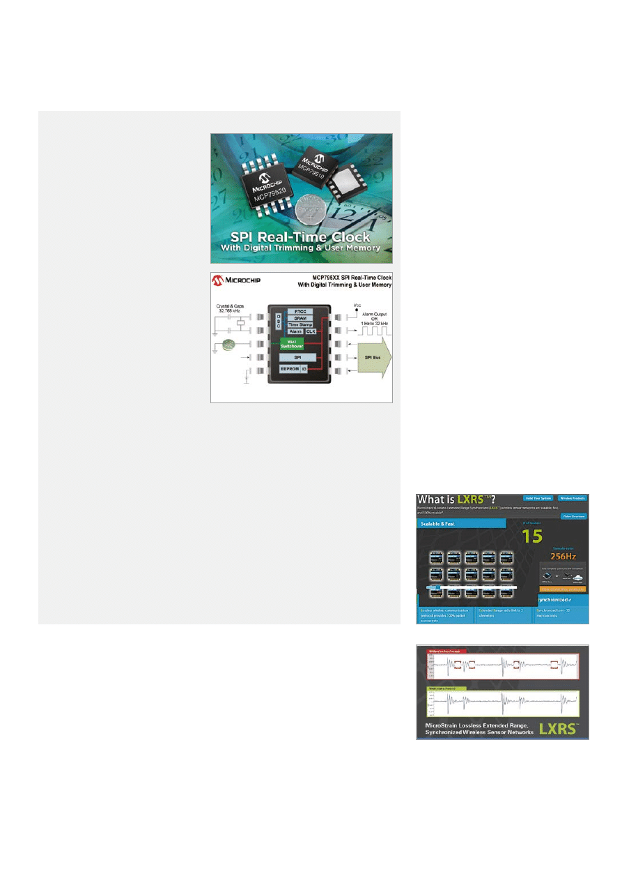
The new LXRS™ Wireless Sensing Sys-
tem (
microstrain.com/what-is-LXRS?
)
includes:
Lossless wireless communication protocol
providing 100% packet success rate under
most operating conditions
Extended Range radio link to 2 kilometers
Scalable wireless sensor networks support-
ing continuous, burst, and hybrid sampling
modes
Time Synchronized to ±32 microseconds
The LXRS™ Wireless Sensing System works
by leveraging an advanced bi-directional
radio communication protocol. When
data are received without errors by the
WSDA base station
, the WSDA sends an
acknowledgement that these packets were
received. Data that are not acknowledged
remain within each LXRS sensor node’s non-
volatile memory for scheduled re-transmis-
sion without reducing the overall system
bandwidth.
Each wireless node in the network has its
own precision timekeeper and maintains
time synchronization to within ±32 micro-
seconds. Data are time-stamped by each
node at the time of analog-to-digital (A/D)
conversion. Therefore, even when re-trans-
mitted, all data are accurately time stamped
and aggregated into a master file using time
as a unifying variable.
This enables highly reliable data collection
from scalable networks of wireless strain,
acceleration, torque, force, temperature,
etc. to be collected without loss of informa-
tion. This is particularly useful when work-
ing in harsh operating environments, when
the system may be subject to periodic RF
interference, and when the experiment or
test is very difficult to set-up or very expen-
sive to replicate.
Synchronized data collection, combined
with robust and reliable LXRS data acquisi-
tion, allows users to select lower sampling
rates and reduced RF power levels. This
leads to longer battery lifetimes and also
enables energy harvesters to be used in
place of primary batteries.
www.microstrain.com - (120532-II)
SPI real-time clock/calendars in smaller,
10-pin packages
Microchip recently announced the
expansion of its stand-alone Real-Time
Clock/Calendar (RTCC) portfolio with
the new 10-pin, SPI MCP795XX fam-
ily. These new devices offer many of
the same features as the larger 14-pin
MCP795WXX family, including supe-
rior timekeeping performance.
Reducing overall component count in
the system and eliminating the user
programming costs for a serial ID
make the MCP795XX RTCC family an
ideal choice for the handheld, wireless
and consumer markets. By including
64 bytes of SRAM, 2 Kbits of EEPROM
and a 128-bit Unique ID, which can be
ordered blank or preprogrammed with
a MAC address, extra memory devices
may not be needed. Utility power
meters, manufacturing equipment,
radios, GPS and hospital instrumenta-
tion applications that need accurate
time over a broad temperature range will also benefit from the very wide digital trim-
ming range, which can compensate up to 22 seconds per day for crystal frequency drift.
Digital trimming improves the timekeeping accuracy of RTCCs, and a wide digital trim-
ming range provides customers with high accuracy over a large temperature range.
Accurate timekeeping is also supported at a decreased power-consumption level,
because digital trimming is maintained when the MCP795XX is operating from backup
power on the VBAT input. Additionally, these devices join the industry’s only portfolio
to distinctively offer a battery-backed RTCC with both power-fail and power-restore
timestamps plus three types of non-volatile memory: EEPROM, SRAM and a Unique ID.
When the time and duration of power failures need to be logged, the MCP795XX fam-
ily can accomplish this without adding any circuitry by using the on-chip power-fail
timestamp feature, which is not offered by any other SPI RTCC on the market. With
long battery life at a premium, applications such as wireless, portable communications,
security and automotive can benefit from the 5 MHz SPI bus and millisecond alarm. This
high-resolution alarm output provides a greater degree of control over the duty cycle
needed to support longer MCU sleep and power-down modes.
http://www.microchip.com/get/0CX3 - (120532-I)

international payment via
+49 (0)4422 955-333
+49 (0)4422 955-360
Professional quality
@ discount prices!
more than 40 years experience
more than 40000 products in stock
no minimum order charge
fast 24 hour shipment
Daily rates! - Price level: 15.8.2012
Multi-talented ISP programmer
for three programming modes
Programs the popular AVR, STM32, NXP
and LPC microcontroller
Functions:
• FLASH • EEPROM • Fuse bits
• Write lock bits • read
• Read OSCCAL registry
• Chip erase
Workshop supplies
Power supply
Components
Network & PC Technology
Sat and TV Technology
Microcontroller
Measurement
technology
Plug connector
.co.uk
2-channel storage oscilloscope
Storage oscilloscope with excellent performance data, extra
large back-lit colour display and USB interface for the export
of he measuring results
to he PC/notebook.
• Bandwid h: 50 MHz • Rise time: <7 ns
• Sample Range: 1 GS/s
UTD 2052 CEL
Digital multimeter
22000-Count-Display
Measuring device with high
accuracy, analogue bar graph
and Low-Bat-Display.
UT 61E
D
2
2
M
M
a
a
UT 61E
• RMS measurement
• Diode test
• Through buzzer
• Data-Hold •MIN/MAX
• REL function
• Peak value function
• USB interface
• Safety: Cat II 600 V,
CAT III 300 V
AC voltage tester
90-1000 V AC
• Safety: EN 61010-1, CAT III 100
• acoustic/visual signal
• integr. torch
• incl. batteries
PEAKTECH 1030
Neutrik Speaker
• For professional stage / loudspeaker technology
• Easily lockable hrough Quick-Lock System
• Touch-proof contacts
Cable connector with screw connection
NEUTRIK NL-2FC
2-pole
NEUTRIK NL-4FC
4-pole
Chassis socket
• For 2 and 4 pole cable connectors
• Faston connection 4.8 mm
NEUTRIK NL-4MP
All HF connectors under:
http://rch.lt/4W
UG 88U-C59
RG 59
PFL 10
10-pole
All pin connectors
http://rch.lt/4X
10-pole
10 pole
All D-Sub connectors under:
http://rch.lt/4Y
D-SUB BU 09
D-SUB BU 25
KAPPE EMV 09
KAPPE EMV 25
All D-Sub solid metal hoods
http://rch.lt/4Z
for example
for example
for example
for example
DIAMEX PROG-S
DIAMEX ALL-AVR is a USB programming adapter
that can be used for programming the popular AVR-
Controllers by ATMEL.
• AT 90, AT Mega, AT Tiny, ATX Mega
DIAMEX ALL AVR
USB-ISP-Programmer
Extremely economical ISP Programmer for ATMEL
processors that can be programmed using the simple
SPI interface. Notewor hy is he designated on-board
processor with specifi cally developed fi rmware that
enable extremely fast programming cycles.
• AVR STK 500, AT Mega, AT Tiny, AT 90
DIAMEX USB ISP
Made in
Germany!
er:
61010-1, CAT III 1000 V
103
10300
yy: EN
stic/vi
r. torc
batter
61010-1, CAT III 1000 V
sual
al sig
sig
ignal
nal
hh
riiess
PE
PEA
PEA
PEA
PEA
PEA
K
KKKKT
KTE
KTE
KTECH
CH
CH
(~ £235,01)
(~ £16,90)
(~ £15,68)
(~ £23,19)
(~ £7,82)
(~ £2,48)
(~ £4,24)
(~ £1,41)
(~ £0,22)
(~ £0,06)
(~ £0,09)
(~ £0,20)
(~ £1,49)
(~ £1,53)
(~ £62,84)
For consumers: The statutory right of withdrawal for consumers shall apply. All stated prices in € include the legal value added tax, ex works Sande, plus forwarding charges for
the entire shopping cart. Our general terms and conditions shall apply exclusively (under www.reichelt.de/agb in the catalogue or on request). Subject to prior sale. All product
names and logos are property of the respective manufacturers. Images can be similar. Subject to misprint, errors and changes in prices.
reichelt elektronik GmbH & Co. KG, Elektronikring 1, 26452 Sande (HRA 200654 Oldenburg)
299,
00
79,
95
9,
95
3,15
5,40
1,80
0,28
0,08
0,12
0,26
1,90
1,95
21,
50
29,
50
19,
95
2 29
12
10-2012 elektor
NEWS & NEW PRODUCTS
Low-pressure-drop
digital flow meter
Swiss sensor manufacturer Sensirion is
launching the new digital SFM3000 mass
flow meter for high-volume applications in
medical devices, process automation and
burner control. The flow channel is designed
to achieve a very low pressure drop of less
than 3mbar through the sensor element.
The flow meter bi-directionally measures
the flow of air and other non-aggressive
gases at rates up to 200 slm with high accu-
racy and very high speed. It outputs a 14-bit
digital signal at a 2 kHz update rate. The sig-
nal is internally linearized and temperature
compensated. Furthermore, the new mass
flow meter operates from a 5 Vdc supply
voltage and features a digital 2-wire inter-
face, making it easy to connect directly to a
microcontroller.
The outstanding performance of the
SFM3000 gas flow sensor is based on Sen-
sirion’s patented CMOSens® Technology,
which combines the sensor element, signal
processing and digital calibration on a tiny
microchip. Gas flow is measured by a ther-
mal sensor element to provide an extended
dynamic range and enhanced long-term
stability compared to other flow measuring
technologies. Thanks to the proven CMOS-
ens® technology, the flow meter is suited
for high-quality mass production and is the
ideal choice for demanding and cost-sensi-
tive OEM applications in medical ventilation
and anesthesia, as well as process automa-
tion and burner control.
www.sensirion.com/en/sfm3000 - (120532-V)
In addition to the annual Jumbo edition of Hexadoku, Elektor’s
July & August 2012 edition also featured a rather different type
of puzzle: the Maze of the Lost Electronics Technician. Our readers
were faced with a maze consisting of passive components: diodes,
zener diodes, resistors, coils, capacitors and the odd pushbutton.
The challenge was to find the input to which 20 volts had to be
applied to make a current flow at the output.
Hundreds of readers entered the maze and managed to find the
way out successfully. The correct solution was: input 2.
The winner of the
Electronic Workstation – Desktop worth £800
and a
Protostation Advanced Breadboard worth £125,
both kindly sponsored by Matrix Multimedia, is:
Evan Wasserman
of Lakewood, New Jersey, USA.
Evan’s estimate of the total number of correct solutions received
was closest to the actual figure. Congratulations, your prizes are
on the way to you.
(120537)
The Electronics Maze Solved
www.elektor.com

From simple to complex applications, nothing can handle your measurements more
effectively than the National Instruments data acquisition platform. Whatever your
budget, channel count, or performance requirements, its unparalleled high-performance
I/O and ability to increase productivity through software measures up to the challenge.
This combination can help you balance performance and investment to deliver precision
accuracy that is scalable and always trustworthy.
Designed for Performance.
Learn more about NI LabVIEW or improve your
existing skills at 9 locations: uk.ni.com/devdays
JOIN THE CONVERSATION: Follow us on
Search
niukie
©2012 Na ional Instruments. All ights reserved. CompactRIO, LabVIEW, Na ional Inst uments, NI, and ni.com a e t ademarks of Na ional Inst uments.
O her product and company names listed are trademarks or trade names of heir respec ive companies. 1684
>> Download The Complete Guide to Building a Measurement System at ni.com/daq
01635 517300
uk.ni.com
info.uk@ni.com
NE
W
Lab
VI
EW
201
2
NO
W
RE
LE
AS
ED
Whatever you’re measuring,
we have the solution.
2 29
14
10-2012 elektor
Computers
USB Isolator
Avoid interference and earth loops
The project itself is a spin-off from an ear-
lier design for a portable oscilloscope for
Android. During the development of that
project we also encountered the problems
of earth loop noise when a charger or PC
was connected. But what was the best point
where to introduce isolation, the digital USB
connection or the analogue section? After
some serious analysis we came to the con-
clusion that it was better to isolate the USB
bus rather than the analogue part.
A popular chip from Analog Devices, the
ADuM3160, was chosen to provide the iso-
lation of the data lines. It supports both Low
and Full speed USB connections. A flyback
converter with a LT3575 as controller was
used to isolate the power supply.
Special IC
The ADuM3160 [1] used in this project, and
its bigger brother the ADuM4160, are, as far
as we know, the only dedicated USB isola-
tors currently available in the marketplace.
These chips can also be found inside most
commercially available USB isolators. The
chips support Low-speed (1.5 Mbit/s) and
Full-speed (12 Mbit/s) USB. According to
By Raymond Vermeulen (Elektor Labs)
If your USB device ever
suffers from noise caused
by an earth loop or if you
want to protect your PC
against external voltages
then you need a USB isolator.
The circuit described here offers
an optimal electrical isolation of
both the data lines as well as the
supply lines between the PC and the
USB device.
Specifications
•Electrically isolated data and power supply lines
•Configurable data rate of 1.5 Mbit/s or 12 Mbit/s
•Power for the device side can be taken from an extra USB host connection or an external
AC power adapter (5 V/min. 0.5 A)
•Transformer isolation = 1500 V
AC
for 1 min
•ADuM3160 isolation = 565 V
peak
for 50 years
•Maximum output current I
out
= 500 mA @ 5 V
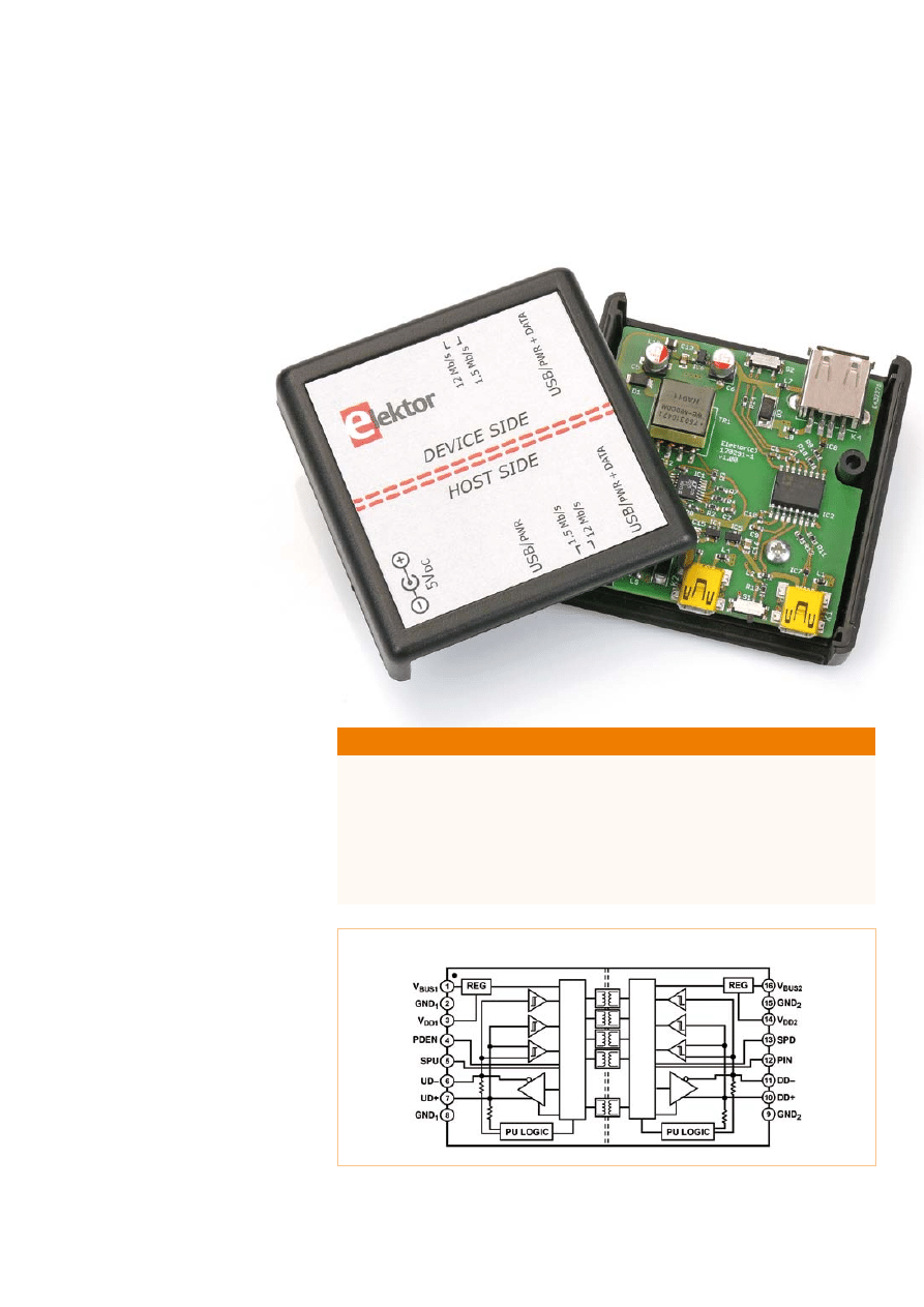
Figure 1. Internal block diagram of the ADuM3160. A number of monolithic transformers
provide the electrical isolation between the two sides of the device.
15
elektor 10-2012
usB isolAtor
Analog Devices the reason why High-speed
(480 Mbit/s) USB is not supported is due to
the fact that there are currently no digital
isolators available that can operate reliably
at these high data rates. There are currently
no plans to introduce a new IC for this.
In Figure 1 you can see the internal block
diagram for the IC. The combination of
high-speed CMOS technology with air core
transformers (the iCoupler technology
from AD) results in an outstanding isolation
between the primary and secondary sides.
To detect the direction of the data flow
over the USB lines (in order to turn on the
appropriate output buffers) the IC deter-
mines the direction based on the contents
of received data packets. The propagation
delay (the time taken for the received sig-
nal to appear at the output) is fairly small
despite the stringent isolation require-
ments, and is comparable to that found in
a standard USB hub.
Circuit diagram and power supply
You may wonder why the power supply is
specifically mentioned in the heading for
K3
2
3
1
L6
33R 100MHz
L5
33R 100MHz
D4
5V6
3SMAJ5919B
C14
10u
6V3
HSN10AAT1G
NCP380
IC3
FLAG
OUT
GND
IN
EN
2
3
1
5
4
K2
1
2
3
4
5
L3
33R 100MHz
L4
33R 100MHz
C15
10u
6V3
HSN05AAT1G
NCP380
IC4
FLAG
OUT
GND
IN
EN
2
3
1
5
4
K1
1
2
3
4
5
L2
33R 100MHz
L1
33R 100MHz
C16
10u
6V3
HSN05AAT1G
NCP380
IC5
FLAG
OUT
GND
IN
EN
2
3
1
5
4
R13
4k7
R14
4k7
S1
2
3
1
R12
24R
R11
24R
C9
100n 25V
C10
100n 25V
C7
100n 25V
S2
2
3
1
USB mini
USB mini
VBUS
K4
GND
D–
D+
1
2
3
4
USB-A
R10
24R
R9
24R
L7
33R 100MHz
L8
33R 100MHz
D3
5V6 3SMAJ5919B
C8
100n 25V
ADUM3160
GND1-1
GND1-0
GND2-1
GND2-0
VBUS1
VBUS2
IC2
PDEN
VDD1
VDD2
PIN
SPD
DD–
SPU
UD–
UD+
DD+
11
12
13
14
16
10
15
1
8
4
5
3
6
7
2
9
R7
28k7
R8
28k7
R4
6k04
R2
33k
R3
80k6
C2
10n
16V
C11
100n 25V
C12
100n 25V
SHDN/UVLO
EX PAD
LT3575
R_ILIM
R_REF
IC1
BIAS
SW_0
SW_1
R_FB
TEST
NC_0
NC_1
NC_2
GND
VIN
17
14
10
TC
12
SS
11
13
15
16
VC
5
3
6
2
4
8
7
1
9
C1
10n
16V
R6
90k9
R5
200k
C4
120u 6V3
L9
1uH
TR1
3 : 1
6
7
3
1
4
2
8
5
D2
PMEG6010CEH
C3
220n
50V
R1
1k
D1
PMEG3050BEP
C5
120u 6V3
L10
1uH
C13
10u
6V3
HSN05AAT1G
NCP380
IC6
FLAG
OUT
GND
IN
EN
2
3
1
5
4
C6
120u 6V3
TPD2EUSB30ADRTR
IC8
GND
D+
D–
1
2
3
TPD2EUSB30ADRTR
IC7
GND
D+
D–
1
2
3
120291 - 11
PRI
AUX
SEC
2
2
2
2
2
2
2
2
2
2
VBUS1
VBUS1
VBUS2
VBUS2
VBUS1
1
1
1
1
1
1
1
1
1
1
1
1
1
1
1
1
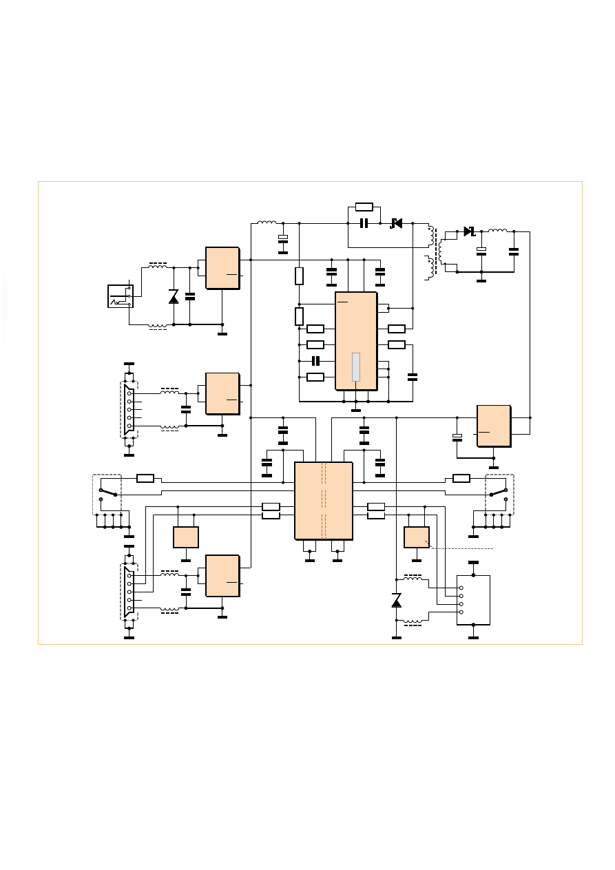
Figure 2. The circuit diagram for the USB isolator. At its heart is a special IC from Analog Devices (IC2),
which provides electrical isolation of the USB signals.
16
10-2012 elektor
Computers
this section. It’s because it plays such a sig-
nificant role in this design. The ADuM3160
can only provide isolation for the data lines
and not for the supply line. You could pro-
vide each side of the IC with its own, sepa-
rate power supply.
In this case (see Figure 2) we decided to
add an isolated switching power supply to
the board. This not only provides power for
the other half of the IC, but also provides
the maximum permitted current for the
USB device connected to it (which is also
completely isolated from the input!).
To obtain the required 500 mA at 5 V from
the output we have chosen a LT3575 fly-
back converter from Linear Technology [2].
Remarkably this IC doesn’t require an opto-
coupler for a feedback signal. The converter
operates in a so-called boundary mode,
where the information regarding the out-
put voltage of the secondary inductor is fed
back to the primary inductor. This works as
follows:
When the power switch in the converter
turns off, the voltage rises to a level that is
equal to:
V
FLBK
= (V
OUT
+ V
F
+ I
SEC
× ESR) × N
ps
where
•
V
F
= voltage across diode D1;
•
I
SEC
= current through the secondary
winding;
•
ESR = total impedance of the secondary
side;
COMPONENT LIST
Resistors
(1% 0.1W, SMD 0603, unless otherwise
shown)
R1 = 1kΩ 1% 0.5W (SMD 1206)
R2 = 33kΩ
R3 = 80.6kΩ
R4 = 6.04kΩ
R5 = 200kΩ
R6 = 90.9kΩ
R7,R8 = 28.7kΩ
R9,R10,R11,R12 = 24Ω
R13,R14 = 4.7kΩ
Capacitors
C1,C2 = 10nF 16V X7R (SMD 0603)
C3 = 220nF 50V X5R (SMD 0603)
C4,C5,C6 = 120µF 6.3V (Nichicon RFS-
0J121MCN1GS, type C)
C7,C8,C9,C10,C11,C12 = 100nF 25V X7R
(SMD 0603)
C13,C14,C15,C16 = 10µF 6.3V X5R (SMD
0805)
Inductors
L1,L2,L3,L4,L5,L6,L7,L8 = ferrite inductor
33Ω@100MHz (SMD 0603) e.g. Murata
BLM18PG330SN1D
L9,L10 = 1µH 1.2A (SMD 1007) e.g. Taiyo
Yuden CB2518T1R0M
Semiconductors
D1 = PMEG3050BEP (NXP) (SOD-128)
D2 = PMEG6010CEH (NXP) (SOD-123f)
D3,D4 = 5.6V 3W zener diode
IC1 = LT3575EFE#PBF (LT) (TTSOP-16)
IC2 = ADUM3160BRWZ (AD) (SOICW-16)
IC3 = NCP380HSN10AAT1G (On Semiconduc-
tor) (TSOP-5)
IC4,IC5,IC6 = NCP380HSN05AAT1G (On Semi-
conductor) (TSOP-5)
IC7,IC8 = TPD2EUSB30ADRTR (TI) (SOT-3)
Miscellaneous
S1,S2 = slide switch with changeover contact
(e.g. C&K Components PCM12SMTR)
K1,K2 = USB mini-B-connector, PCB mount
(e.g. On-Shore USB-M26FTR)
K3 = DC adapter connector, 1.35 mm (e.g. CUI
PJ-014DH-SMT)
K4 = USB-A connector, PCB mount (e.g. FCI
87583-2010BLF)
TR1 = transformer 3:1, 25 µH (e.g. Würth
750310471)
Case, Hammond type 1593KBK
2 self tapping screws, cross head, 4x6.4mm,
DIN7981
PCB # 120291-1 or
assembled and tested board and case, #
120291-91
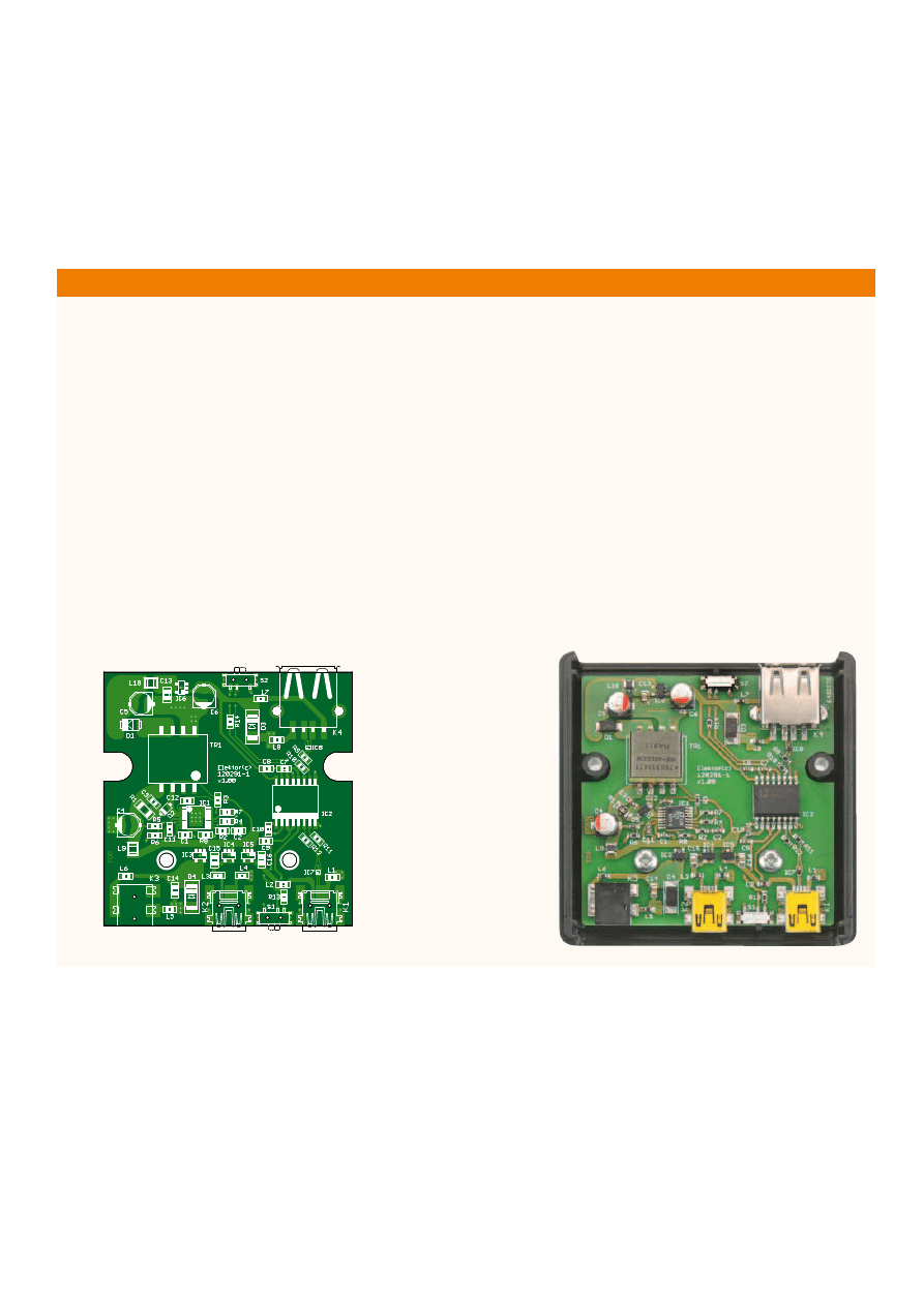
Figure 3.
The dimensions of the
board were chosen to fit
in a type 1593KBK case
from Hammond.
17
elektor 10-2012
usB isolAtor
•
N
PS
= turns ratio of the primary
and secondary windings of the
transformer.
In conjunction with the tempera-
ture compensation this provides
enough information to regulate the
output voltage. One consequence of
this method is that the switch has to
be turned off for a certain minimum
amount of time during each cycle, to
give the IC sufficient time to process
the feedback information.
An off the shelf transformer from
Würth was chosen, which is a small
potted type for SMD mounting.
The data lines are protected from high
input voltages by IC7 and IC8. These
are two-channel ESD protection ICs
(TPD2EUSB30A) from TI (this part
would also be suitable for USB3 data
lines). The dimensions of this IC are so
small (1 x 1 mm!) that it can easily be put
between the data lines on the PCB.
All power supply connections are pro-
tected against overloading with the help
of high-side power distribution switches
(NCP380) from ON Semiconductor. These
ICs include a detection and control circuit
with a P-channel MOSFET that limits the
output current when it exceeds a preset
value. Two different types of the NCP380
have been used in this circuit: IC4, 5 and 6
limit the current to 0.5 A, IC3 to 1 A. These
provide optimum protection to al inputs
and outputs (both USB and supply) against
(almost) all possible types of overload.
In this way, the USB ports are limited to
500 mA and the 5 V
DC
connection is limited
to 1000 mA. A connected USB device always
has 500 mA available to it, which doesn’t
quite conform to the official USB standards.
Initially, the limit should really be 100 mA.
It should be increased to 500 mA only after
the device has announced itself to the host
and requested the current increase. How-
ever, in practice it seems that you can nor-
mally get 500 mA from a USB port on your
PC without the need for any requests.
In order to keep ripple to a minimum at the
primary and secondary side of the switch-
ing power supply, we’ve added LC filters to
both sides (L9/C4 and L10/C13). The ripple
currents through capacitors C4 and C5 are
very large, which you have to keep in mind
when you select the types for these. It is
best to use capacitors with the lowest pos-
sible ESR. To keep the turn-off spike at the
primary side of the supply within manage-
able levels, an RCD snubber network has
been added, consisting of R1, C3 and D2.
Construction
For a circuit that has so many special ICs
(all SMD) it is a ‘must’ to have a thought-
fully designed board layout. In Figure 3
you can see the board that was designed
in the Elektor Labs. It is of course possible
to obtain this board separately and pop-
ulate it yourself. However, since several
components are very tricky to solder due
to their size, and some are also not easily
obtainable, Elektor has made a fully popu-
lated board available, including the case.
All you need to do is to add a few holes for
the connectors and slide switches in the
two side panels of the case. To be on the
safe side, the two tags of K4 that come
through the board should be soldered
using an ordinary soldering iron. The
board can then be fixed inside the case
using the two screws provided.
The drawing in Figure 4 can be copied and
stuck to the top of the case. The original
design for the drawing can also be down-
loaded from the Elektor website [3]
accompanying this project.
Usage
It is very easy to use the USB isola-
tor. First, set the required speed with
switches S1 and S2.
Both of these should always be set to
the same speed!
Normally a USB device can let the host
know at which speed it operates via
a pull-up resistor on one of its data
lines. This isn’t possible with this iso-
lator and the speed has to be set man-
ually via switches (this is also the case
for most commercially available USB
isolators).
Connect the ‘host’ (in most cases this
is your PC) to K1 (HOST SIDE: USB/
PWR+DATA) and the isolated USB device to
K4 (DEVICE SIDE: USB/PWR+DATA). If the
device needs more than 300 mA we sug-
gest that you connect an extra USB cable to
K2 (USB/PWR) or connect a regulated 5 V
power adapter (min. 500 mA) to power sup-
ply connector K3 (5 V
DC
).
We recommend that you don’t use this
project in situations where there may be
voltage differences between the host and
device side that are greater than the AC line
voltage. You should also not subject the
device to high voltage differences between
the host and device side for extended peri-
ods of time, because the isolation can
deteriorate over time if the components
are continuously exposed to high voltage
differentials.
(120291)
Internet Links
[1] www.analog.com/static/imported-files/
data_sheets/ADuM3160.pdf
[2] http://cds.linear.com/docs/
Datasheet/3575f.pdf
[3] www.elektor.com/120291
HOST SIDE
DEVICE SIDE
USB
/
PWR
12
Mb/s
1.5
Mb/s
5V
D
C
USB
/
PWR
+
D
AT
A
USB
/
PWR
+
D
AT
A
12
Mb/s
1.5
Mb/s
Figure 4. Print this out and stick it to the top of the
case for the professional look.

18
10-2012 elektor
Microcontrollers
Embedded Linux
Made Easy (4)
A look at the kernel
By Benedikt Sauter [1]
GNU/Linux provides interfaces and applications
for devices that we are used to seeing on desktop
computers and servers. Much of this transfers to
the embedded domain, where Linux relieves the
programmer of a lot of work by handling networking,
USB, Bluetooth and more without the need to write
complex dedicated C programs. And as we shall see,
using a modern operating system brings many other
benefits too.
In the previous instalments in the series we have looked at how the
toolchain, the kernel and bootloader, and a standard file system can
be got up and running. One aim of the series is to show developers
what is happening ‘under the bonnet’, for example in how devices
and processes are implemented. In this instalment we will first look
at what advantages there are in using an operating system when
compared to driving hardware at the ‘bare metal’ level.
What is the essence of an operating system? At its heart it consists
of a collection of all the software needed to run specially-written
applications in parallel with others. The distinction between ‘nor-
mal’ firmware and operating-system-based firmware is, however,
somewhat blurred. It is common enough for normal firmware to
include a clean interface to the hardware layer to provide com-
monly-wanted functions, for example in memory management;
and often there will be a small scheduler to divide the processor’s
attention between different programs. Together these already form
the beginnings of what might be called an ‘operating system’.
A typical operating system
There are of course many books on the subject of operating sys-
tems [2]. Here we shall only take a broad overview of the main
components:
•
Device management
•
Process management
•
Memory management
•
File management
•
User and permissions management
In the embedded world device management is usually a particularly
important aspect. The operating system must present peripherals
and hardware to applications in such a way as to simplify their use
as far as possible. This is done using device drivers. The operating
system is also responsible for handling all the details behind allow-
ing several programs to run simultaneously, all wanting access to
SD cards, network interfaces and so on.
In the simplest programming model, an application running under
an operating system is a single, independently executable process.
A process has its own virtual address space, ensuring that it cannot
disturb other processes. Processes are centrally managed via the
process table, and each has its own ‘process control block’ [3] which
typically includes space for temporary storage of processor register
contents and other important variables:
•
Program counter
•
CPU registers
•
Stack pointer
•
Status of open files
•
Process state
•
Other status information
When we launch our ‘hello world’ program the kernel loads the
application and creates a new process. A new process is always cre-
ated on the basis of the current one, and inherits the user permis-
sions associated with it. The command
ps -ejH
will display the current set of processes in the system in a tree struc-
ture. At the root of the tree is the first process launched by the ker-
19
elektor 10-2012
eMbedded linux MAde eAsy
nel, invariably called ‘/sbin/init’. Starting this process is one of the
first things the kernel does when booted.
As developers we are particularly interested in the following fea-
tures of an operating system:
•
The interface for device drivers
•
The file system for programs and data
•
Launching and executing programs
•
Shared use of libraries by different programs
•
Access to input and output ports
•
Transferring working memory to non-volatile memory
•
Memory management for applications and processes
•
Process management
Let us start with device management.
Configuring the kernel
Which interfaces and peripheral blocks of the embedded processor
we need will depend on the application. The Linux kernel is designed
in a modular fashion, which results in the developer having very
fine control over its settings and in particular over what drivers and
mechanisms will be included in the kernel. It is also subsequently
possible to load other components dynamically. The best way to
see how this is done is to look directly in the kernel source code. So,
switch to the kernel source code tree:
cd ElektorLinuxBoardDownload_20120509
cd linux-2.6.33-lpc3131x
and invoke the kernel configuration menu:
make menuconfig
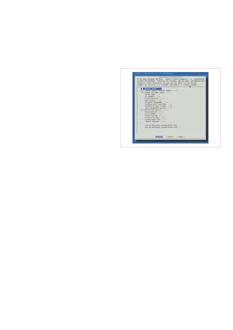
The main menu (Figure 1) should immediately appear. If it fails to
appear, one possible cause is that the libraries for displaying con-
sole-style menus are missing. They can be installed on our Ubuntu
system by typing:
sudo apt-get install libncurses5-dev
From the main kernel configuration menu it is possible to enable or
disable any of its features and device drivers at will. For the beginner
it will not always be immediately obvious where within the menu
structure a particular option might be hiding, but with a bit of prac-
tice it soon becomes familiar.
An alternative to using the menu is to go straight to the config-
uration file ‘.config’ in the kernel source directory (linux-2.6.33-
lpc3131x) and edit it by hand. (The full stop at the start of ‘.config’
indicates that it is normally a ‘hidden file’.) However, it is usually
more convenient to use the interactive menu. Before changing the
configuration it is a good idea to make a backup copy of the current
configuration file.
cp .config config_backup
Newcomers to Linux often ask where good documentation can be
found. The best documentation for the kernel is in the kernel source
itself. It is also possible to click on ‘help’ at any time in the menu to
find information on a particular item, or you can browse through
the ‘Documentation’ directory (at the top level of the kernel source
tree) to look for information on a particular topic.
As Figure 1 shows, the menu items are sorted into groups. At the
top are the general kernel settings, and then follow settings for the
device drivers and file systems, and finally items relating to cryp-
tography and security.
General setup
The menu item ‘General setup’ covers the basic characteristics of
the kernel, including, for example, whether there is any swap space,
how memory is managed and how internal communications are car-
ried out. There are also settings relating to the kernel image itself,
optimisations for small systems, statistics, tools and much more
besides. The more you find out about the Linux kernel, the more
handy features you discover: there are only a few people who can
lay claim to understanding it completely!
Enable loadable module support
Another good feature of Linux is that the kernel can be extended,
while it is running, by simply adding extra modules. The kernel
configuration menu lets you decide whether a particular feature
or driver should be permanently built into the kernel code or com-
piled as a module: an ‘M’ before a menu item means that the feature
will be compiled as a module, whereas an asterisk before an item
means that it will be built in permanently. If you want to be able
Figure 1. Main kernel configuration menu.
20
10-2012 elektor
Microcontrollers
to support a wide range of different devices, building all the driv-
ers into the kernel can make it unwieldy: it is better to compile the
drivers as modules and load them manually or let the kernel load
them automatically.
Enable the block layer
The kernel distinguishes between two types of device: character
devices and block devices. A character device sends and receives
messages and other data one character at a time; a block device
always does so in complete blocks. Typical character devices include
consoles and UART interfaces; block devices include hard disks and
memory cards such as MMC and SD cards. If no block devices are
needed (as is possible for some embedded systems) some memory
space can be saved by disabling the ‘block layer’.
System type
Some kernel features depend on the type of processor being used.
For example, it may be desirable to enable or disable caches or
memory management units. This menu item lets you specify (as
far as is possible) the processor type: if your particular processor is
not listed, you will need to find a patch or suitable ‘board support
package’ (or write it yourself).
Bus support
Here it is possible to enable support for typical PC-type buses. In our
case only the PCMCIA option is available.
Kernel features
This item is very kernel-specific: you can specify what binary inter-
face convention is to be presented to programs and other miscella-
neous features, such as displaying processor load via the blink fre-
quency of an attached LED.
Boot options
How the kernel is started up depends in the case of the Elektor Linux
board chiefly on the bootloader. The main interface between the
bootloader and the kernel is the so-called ‘kernel command line’.
This command allows the bootloader to pass various parameters to
the kernel that can subsequently be examined by it or by other pro-
grams. The menu item allows you to specify that a given different
command line should be used instead. Alternatively, it is possible to
compile the kernel so that it can be run directly from flash storage.
CPU Power Management
These days processors offer an ever wider range of features to sup-
port efficient power management. The kernel has to be properly
configured to allow applications to take full advantage of these
features.
Floating point emulation
This kernel configuration menu option allows you to configure it so
that it takes responsibility for floating-point calculations or so that
hardware support is used. At least one of these alternatives must be
selected to allow programs to be run.
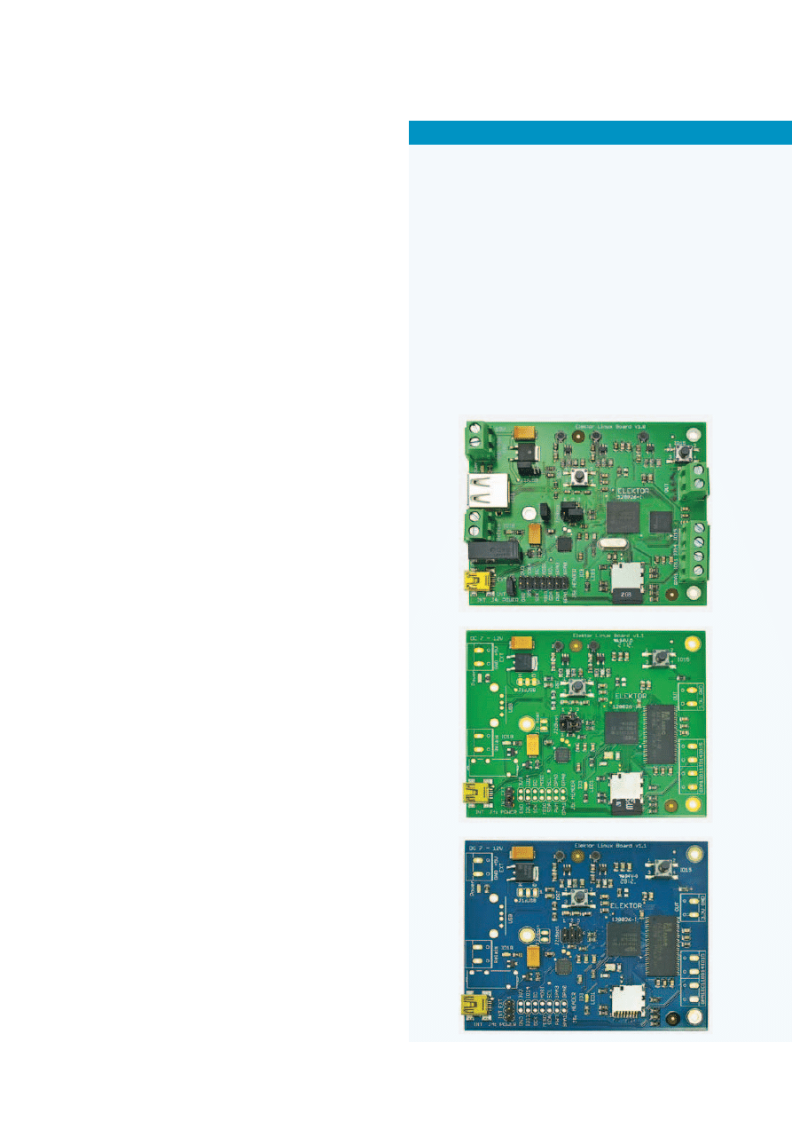
New version of the Elektor Linux board
Demand for the Elektor Linux board has been truly overwhelming!
Because of the large number of orders we have received the next
production batch has had to be made rather sooner than expected.
Unfortunately the DRAM chip in the BGA package has a lead time
of some 20 weeks, and so we decided to change the layout to ac-
cept a TSOP54 device. The new memory has the same capacity as
the old one but requires a supply voltage of 3.3 V instead of 1.8 V.
The upper picture shows the original version of the board with the
BGA memory chip, while the version in the middle picture has the
TSOP54 device fitted. Since the beginning of July we have been de-
livering version ‘1.1 blue’ of the board, in which the now redundant
1.8 V voltage regulator circuitry is removed. You can easily identify
the most recent version of the Elektor Linux board by its blue colour.
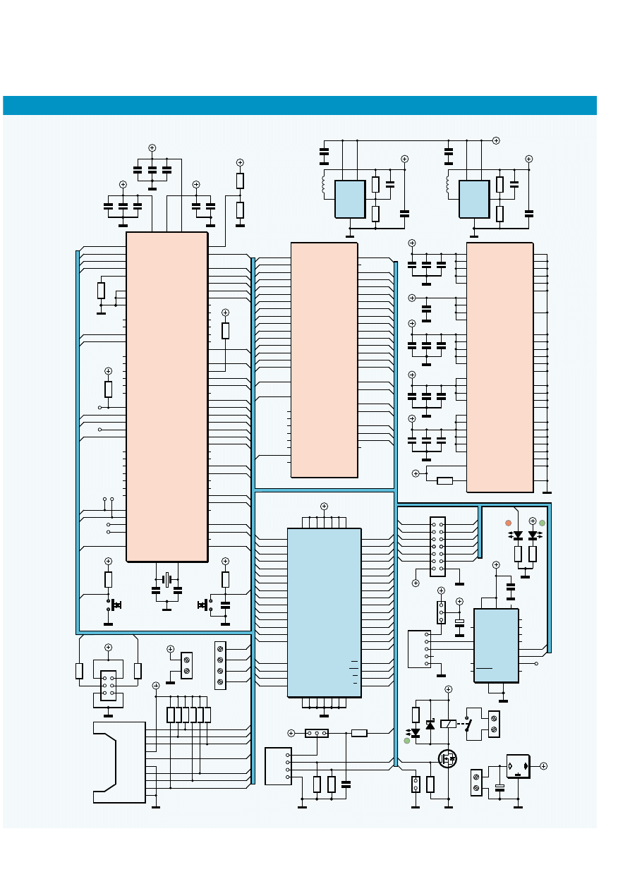
The corresponding circuit diagram is shown here.
21
elektor 10-2012
eMbedded linux MAde eAsy
A43E26161
VDDQ
VDD
VDDQ
VDDQ
VDDQ
VDD
VDD
VSS
VSSQ
VSSQ
VSSQ
VSSQ
VSS
VSS
IC5
DRAM
DQ10
DQ11
DQ12
DQ13
DQ14
DQ15
LDQM
UDQM
RAS1
DQ0
DQ1
DQ2
DQ3
DQ4
DQ5
DQ6
DQ7
A10/AP
NC
A11
BS0
BS1
DQ8
DQ9
CLK
CKE
CAS
23 A0
3
2
4
5
7
8
10
11
13
24 A1
25 A2
26 A3
29 A4
30 A5
31 A6
32 A7
33 A8
34 A9
22
36
35
20
21
42
44
45
47
48
50
51
53
1
9
49
43
14
27
15
39
38
37
17
18
WE 16
CS
19
28
6
12
46
52
41
54
EBI_NCAS_BLOUT_0
EBI_NRAS_BLOUT_1
LPC313XFET180
EBI_DQM_0_NOE
MNAND_RYBN2
MNAND_RYBN0
MNAND_RYBN1
MNAND_RYBN3
EBI_A_0_ALE
EBI_A_1_CLE
NAND_NCS_0
NAND_NCS_1
NAND_NCS_2
NAND_NCS_3
MLCD_DB_10
MLCD_DB_11
MLCD_DB_12
MLCD_DB_13
MLCD_DB_14
MLCD_DB_15
MLCD_RW_WR
MLCD_DB_0
MLCD_DB_1
MLCD_DB_2
MLCD_DB_3
MLCD_DB_4
MLCD_DB_5
MLCD_DB_6
MLCD_DB_7
MLCD_DB_8
MLCD_DB_9
MLCD_E_RD
EBI_D_10
EBI_D_11
EBI_D_12
EBI_D_13
EBI_D_14
EBI_D_15
MLCD_CSB
EBI_D_0
EBI_D_1
EBI_D_2
EBI_D_3
EBI_D_4
EBI_D_5
EBI_D_6
EBI_D_7
EBI_D_8
EBI_D_9
EBI_NWE
MLCD_RS
IC6.B
G2
F2
F1
E1
E2
D1
D2
C1
B1
A3
A1
C2
G3
D3
E3
F3
H1
J2
B4
J1
J3
K1
K2
E6
E7
D4
N8
P9
N6
P6
N7
P7
K6
P5
N5
L5
K7
N4
K5
P4
P3
N3
B3
A2
P8
N9
L8
K8
G1
H2
C19
10n
C18
100n
C21
10u
C38
100n
C31
10n
C33
100n
C32
10u
C25
10n
C26
100n
C27
10u
C17
10n
C22
100n
C23
10u
+3V3
Q2
12MHz
C30
22p
C29
22p
C15
47n
C16
100n
C14
10u
C13
10u
C12
3n3
+3V3
+3V3
C36
220p
C35
1n
C37
10u
+1V2
+1V2
+1V2
+3V3
+3V3
+3V3
R19
10R
+3V3
+3V3
X7
1
2
3.3V
GND
X4
1
2
3
4
LPC_D0
LPC_A1
LPC_D2
LPC_D3
LPC_D4
LPC_D5
LPC_D6
LPC_D7
LPC_D8
LPC_D9
LPC_D10
LPC_D11
LPC_D12
LPC_D13
LPC_D14
LPC_D15
LPC_CAS
LPC_RAS
LPC_WE
LPC_CS
LPC_A0
LPC_A1
LPC_A2
LPC_A3
LPC_A4
LPC_A5
LPC_A6
LPC_A7
LPC_A8
LPC_A9
LPC_A10
LPC_A11
LPC_A13
LPC_A14
LPC_A12
LPC_DQM0
LPC_DQM1
LPC_CLK
LPC_CKE
LPC_A0
LPC_A1
LPC_A2
LPC_A3
LPC_A4
LPC_A5
LPC_A6
LPC_A7
LPC_A8
LPC_A9
LPC_A10
LPC_A11
LPC_A12
LPC_A13
LPC_A14
LPC_A15
LPC_D0
LPC_D1
LPC_D2
LPC_D3
LPC_D4
LPC_D5
LPC_D6
LPC_D7
LPC_D8
LPC_D9
LPC_D10
LPC_D11
LPC_D12
LPC_D13
LPC_D14
LPC_D15
LPC_CLK
LPC_DQM0
LPC_WE
LPC_MC1_CD
LPC_CS
LPC_DQM1
LPC_CKE
LPC_CAS
LPC_RAS
DAT2
DAT3
DAT0
DAT1
SW_A
SW_B
U1
CMD
CLK
GND
V+
1
2
3
4
5
6
7
8
SD-CardSocket
DM3D-SF
LPC_MCI_DAT2
LPC_MCI_DAT3
LPC_MCI_CMD
LPC_MCI_CLK
LPC_MCI_DAT0
LPC_MCI_DAT1
LPC_MCI_CD
+3V3
R21
10k
R30
10k
R23
10k
R25
10k
R29
10k
TRST_N
TDI
TMS
TCK
TDO
SYSCLK_O
R13
DNP
R12
10k
+3V3
R17
10k
GPIO0
R2
10k
+3V3
GPIO2
LED1
LPC_MCI_CLK
LPC_MCI_CMD
LPC_MCI_DAT0
LPC_MCI_DAT1
LPC_MCI_DAT2
LPC_MCI_DAT3
GPIO11
GPIO14
GPIO15
GPIO18
GPIO19
PWM_DATA
GPA0
GPA1
GPA3
C11
100n
RESET
S3
RESET
+3V3
RESET
I2C_SDA
I2C_SCL
R11
12k
USB_ D
LPC_DM
LPC_DP
K1
VCC
GND
D–
D+
1
2
3
4
USB
R10
1M
R14
1M
LPC_DM
LPC_DP
1
2
3
J3
C10
100n
+5V
LPC_VBUS
1%
SPI_SCK
SPI_MISO
SPI_MOSI
LPC_RXD
LPC_TXD
TP1 TP2
TP5
TP6
R26
10k
+3V3
S1
GPIO15
USB_VDDA33-DRV
USB_VDDA12-PLL
LPC313XFET180
USB_VSSA_TERM
USB_VSSA_REF
MI2STX_DATA0
SPI_CS_OUTO
MUART_CTS_N
MUART_RTS_N
I2SRX_DATA1
I2SRX_DATA0
MI2STX_BCK0
MI2STX_CLK0
I2STX_DATA1
CLK_256FS_O
ADC10B-GPA0
ADC10B-GPA1
ADC10B-GPA2
ADC10B-GPA3
USB_VDDA33
I2SRX_BCK1
I2SRX_BCK0
MI2STX_WS0
I2STX_BCK1
BUF_TRST_N
I2SRX_WS0
FFAST_OUT
SPI_CS_IN
I2SRX_WS1
I2STX_WS1
CLOCK_OUT
FFAST_IN
USB_VBUS
USB_RREF
USB_GNDA
I2C_SDA0
I2C_SCL0
I2C_SDA1
I2C_SCL1
SPI_MISO
SPI_MOSI
UART_RXD
UART_TXD
SCAN_TDO
SYSCLK_O
PWM_DATA
SPI_SCK
ARM_TDO
BUF_TCK
BUF_TMS
JTAGSEL
RSTIN_N
MGP O10
USB_DM
USB_DP
USB_ID
TRST_N
MGPIO5
MGPIO6
MGPIO7
MGPIO8
MGPIO9
GPIO11
GPIO12
GPIO13
GPIO14
GPIO15
GPIO16
GPIO17
GPIO18
GPIO19
GPIO20
GPIO0
GPIO1
GPIO2
GPIO3
GPIO4
IC6.A
A10
B10
C10
D10
E12
E13
P12
N12
N13
P14
G14
F14
F13
M10
N10
P11
M13
M12
M11
N14
F12
E14
G10
P13
TDI
TMS
P10
TCK
M14
E11
F10
F11
D13
D14
N11
H12
G13
H14
K10
J10
L14
B11
C11
H13
H10
J12
J14
J13
J11
K12
K14
H11
K13
B14
A14
B13
C14
P1
M2
L1
L2
N2
P2
M1
J5
K4
L3
N1
A7
A8
C8
B8
B7
K9
J4
B6
A6
A5
B5
C5
A4
B9
R1
10k
+3V3
SV1
1
2
3
4
5
6
+3V3
R9
1k
LPC_VBUS
JP1
1
2
USB_ID
R15
10k
R16
10k
GP
O0
GP
O2
TP3
TP4
1
2
3
4
5
6
7
8
9
10
11
12
13
14
J5
+5V
C4
4u7
R6
66k5
R5
301k
C8
22p
+3V3
L3
4uH7
AS1324
VOUT/
IC3
GND
V N
VFB
EN
SW
2
1
5
4
3
C1
10u
C5
4u7
R4
301k
R3
301k
C7
22p
+1V2
L2
4uH7
AS1324
VOUT/
IC2
GND
VIN
VFB
EN
SW
2
1
5
4
3
C2
10u
GPA1
GPIO11
GPIO14
GPIO15
X1
1
2
Q4
BSS123
R18
10k
GPIO18
K4
13
11
7
5
G6D-1A-ASI5VDC
+5V
D4
BAT54
R22
270R
LED5
X6
1
2
MC78M05ABDT
IC8
C20
47u
+5V
EXT
GPA0
GPA3
I2C_SCL
SPI_MOSI
SYSCLK_O
GPIO14
GPA1
PWM_DATA
I2C_SDA
SPI_MISO
SPI_SCK
GPIO11
R20
10k
X2
+5V
GND
D–
D+
4
1
2
3
5
MINI-USB
LPC_RXD
LPC_TXD
TP7
1
2
3
J4
+3V3
+5V
EXT
C24
47u
CD2102
SUSPEND
SUSPEND
REGIN
IC7
VBUS
GND
VDD
EXP
RST
GND
DCD
DTR
DSR
TXD
RXD
RTS
CTS
D-
RI
D+
11
12
28
27
26
25
24
23
5
2
6
7
8
4
9
3
1
ADC10B_VDDA33
LPC313XFET180
ADC10B_GNDA
VDDE_IOA
VDDE_IOA
VDDE_IOA
VDDE_IOA
VDDE_IOA
VDDE_IOB
VDDE_IOB
VDDE_IOB
VDDE_IOB
VDDE_IOC
VDDE_IOC
VDDE_IOC
VDDE_IOC
VDDE_IOC
VDDE_IOC
VSSE_IOA
VSSE_IOA
VSSE_IOA
VSSE_IOA
VSSE_IOA
VSSE_IOA
VSSE_IOB
VSSE_IOB
VSSE_IOB
VSSE_IOB
VSSE_IOC
VSSE_IOC
VSSE_IOC
VSSE_IOC
VSSE_IOC
VSSE_IOC
VSSE_IOC
VDDE_ESD
VDDA12
VDDA12
VSSA12
VPP_A
VPP_B
IC6.C
VDDI
VSSI
VDDI
VDDI
VDDI
VDDI
VSSI
VSSI
VSSI
VSSI
VSSI
A11
A13
L12
C12
D11
E10
C13
G12
L10
D12
L11
B12
G11
L13
A12
K11
H3
L7
C6
A9
C9
B2
E5
F5
G5
H5
L4
M5
M7
M9
D5
D7
E8
C7
G4
L6
C3
C4
E4
F4
H4
K3
M3
M4
M6
M8
D6
D8
D9
L9
E9
+5V
+5V
Relay
C28
1u
DC 7 - 12V
GND
+5V
120181 - 13
LED2
R27
270R
LED1
R24
270R
+3V3
LED1

22
10-2012 elektor
Microcontrollers
User space binary formats
Programs and applications are compiled using the toolchain (see
the previous instalment in this series). Normally, for a Linux system,
the toolchain will produce either a .elf file (‘executable and linka-
ble format’, corresponding roughly to a .exe under Windows) or an
‘a.out file’. The kernel reads these formats and launches the com-
piled application appropriately.
A handy Linux command is
file
which lets you see what format a
given file has. Switch to the appropriate directory using
cd
and then
type
file
followed by the name of the file of interest. For example, in
the Linux directory there is a file called ‘vmlinux’. Typing
file vmlinux
produces the answer
vmlinux: ELF 32-bit LSB executable, ARM, version 1
(SYSV), statically linked, not stripped
The file is an executable file for ARM processors that is statically
linked.
Power management options
It is not just the processor that offers power management features:
many peripherals and other devices have the ability to go into a
sleep mode. The operating system can take a copy of important
data and send the peripheral to sleep. When the time comes to
wake the peripheral up again, the data are copied back from mem-
ory and its state is restored. The exact behaviour of the kernel in
these situations can be configured here.
Networking support
Finally we come to one of the most interesting points for develop-
ers. Under ‘networking support’ we can enable, disable and config-
ure all the software stacks (protocol libraries) for the various com-
munication interfaces, including Ethernet, TCP/IP, CAN, infra-red,
amateur radio, Bluetooth and wireless.
Device Drivers
We are also especially interested in device drivers. This menu item
includes everything you might wish for, from the simplest I/O port
to the most up-to-the-minute high speed server bus. The kernel
source code (see download at [4]) includes drivers for a wide range
of USB, I
2
C and SPI devices which we now have at our disposal.
File systems
File systems are important to us for two reasons. First, the operat-
ing system itself must reside in a file system (on the SD card), so
that the kernel can read the files it needs from it. And second, the
operating system has to use a file system to allow application files
and directories to be stored on a hard disk.
Kernel hacking
This menu item is chiefly aimed at kernel developers.
Security options
Linux includes a range of different security features. The most famil-
iar of these is the system of user and group permissions and the
existence of a ‘root’ user. Applications can be further protected
using techniques such as trusted platform modules and internal
security models.
Cryptographic API
This menu item covers cryptographic functions in the kernel.
Library routines
This menu item includes functions for calculating checksums along-
side many other things.
If you want to save your new kernel configuration, use the last menu
item ‘Save an alternate configuration file’. After entering a name for
the new kernel configuration it will be stored locally in the kernel
source tree.
We described in the previous instalment in this series [4] how to
go about compiling the kernel (
make zImage
) and copying it to an
SD card. If new modules are to be included in the kernel, they have
to be separately compiled and installed. Compile the modules by
typing:
make modules
and to copy them to the SD card, either give the path to the des-
tination SD card directly in the following command, or install the
modules into ‘/tmp’ and then copy the new directory that is created
there to the SD card, either as user ‘root’ or using the ‘sudo’ com-
mand. (It is not that root privileges are required for the copy opera-
tion itself, but rather that we must ensure that the files are copied
to the file system on the SD card in such a way that the kernel can
subsequently use them as the root user.)
make INSTALL_MOD_PATH=/tmp modules_install
Now we switch the the ‘/tmp’ directory and copy the directory lib
to the SD card:
cd /tmp
sudo cp -R lib /
media/86b3be7-00f3-45e0-832e-1f48c2c3065e
with the appropriate change to the long hex string.
Interfaces
Linux has its roots in the PC world. There we are faced with inter-
faces such as IDE, SATA, PCI, AGP and the like. In the embedded
world the focus is more on the traditional microcontroller interfaces
and, of course, USB.

23
elektor 10-2012
eMbedded linux MAde eAsy
To summarise, our board has the following interfaces:
•
USB (as host and device)
•
UART (in its current form as the system console, but can also be
used as an interface to external devices)
•
I
2
C (as master)
•
SPI (as master)
Also, the processor has other hardware functions such as:
•
GPIO
•
A/D converter
•
PWM output
As we proceed we will look more closely at these interfaces.
Device files
In order to allow applications to talk to devices, we need an inter-
face to the device driver. The way that drivers are accessed varies
greatly from one operating system to another. Linux is based on
a UNIX file system, and under UNIX things are particularly simple:
each device is treated as a file. The idea is that no special tools are
required to drive a device; instead, we can just use small, simple
programs (from the console), operating on devices exactly as if they
were files. We showed an example of how this works in the case of
GPIO pins in the second instalment of this series [5], where we dem-
onstrated how to flash an LED.
There are two important commands with which surprisingly much
can be achieved:
cat
and
echo
. The command
cat
displays the con-
tents of a file;
echo
, conversely, lets us write any desired text to a
file. To put it more precisely, the output of
echo
can be redirected
to any desired file.
So, for example, if we want to write some data directly to a hard disk
(that is, not via a file system) or send data to a serial port, we can use
echo
in commands of the form
echo “Data for the hard disk” > /dev/sda
or
echo “Hello there, world” > /dev/ttyS0
But be careful: if you wish to experiment with writing data directly
to a hard disk or memory card, make sure you use one without any
important information stored on it!
Some device files correspond to block devices and some to char-
acter devices. A hard disk, for example, is always treated as a block
device, whereas an RS-232 interface is treated as a character device
like a normal terminal, receiving and processing characters one at a
time. Table 1 gives a list of example device files that might be found
in a typical UNIX or Linux system.
Readers may be wondering exactly what mechanism is hiding
behind the commands
echo
and
cat
. How exactly does a driver send
or receive data? Now, since everything is a file, we can access the
device by simply reading from or writing to it as we would a file. This
means that each driver simply has to provide three functions:
Read
,
Write
and
Ioctl
(which allows the device’s settings to be changed).
Read
and
Write
are the standard functions for reading and writing
files, the process in the case of a device being exactly analogous to
that for a normal file. The first step is to open the device or file and
obtain a ‘handle’ (a number which identifies the opened device or
file). The handle is then passed to subsequent
Read
or
Write
opera-
tions on the device or file.
Kernel space and user space
Classical operating systems (in which category we include Linux) are
generally constructed with a clear separation between the mem-
ory area that is used by the kernel and the memory area available
for applications. An application is not permitted to access the ker-
nel’s memory. This is another important fact for developers work-
ing close to the system level to bear in mind. In Linux, the memory
areas are called ‘kernel space’ and ‘user space’. Usually in the case
of a device driver, all the software will be in kernel space. So how
does a user application program get its hands on the data received
over an interface?
The answer lies in the kernel functions such as
copy_to_user
[6],
which copies a block of data from kernel space into user space. So,
when an application reads a device file the driver must use this func-
tion to make the information available to the application.
Integrating a device driver
We now know the basic principles of operation of a kernel device driver.
The question remains, however, of how the kernel knows to associate
Table 1. Device files typically found in the /dev directory
Device type
File in /dev
Character or block device
IDE hard disk
/dev/hda, /dev/hdb, ...
Block
SCSI hard disk
/dev/sda, /dev/sdb, ...
Block
RS-232 interface
/dev/ttyS0, /dev/ttyS1, ...
Character
Printer
/dev/lp0, /dev/lp1
Character
Camera
/dev/video0, /dev/video1
Block
Mouse
/dev/input/mice
Character
RAM
/dev/ram
Block
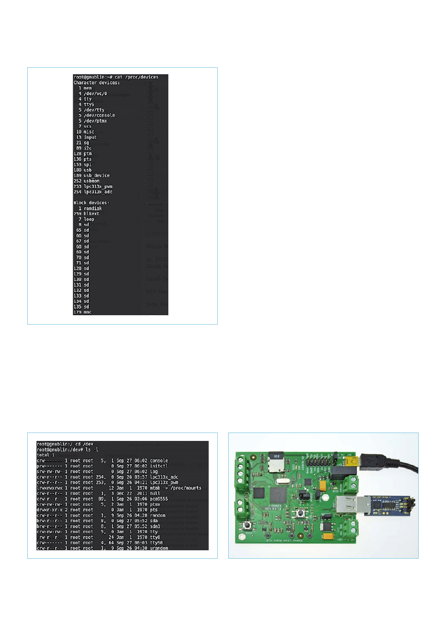
24
10-2012 elektor
Microcontrollers
a file such as
/dev/ttyS0
with the correct driver for the serial port.
To this end so-called ‘major’ and ‘minor’ device numbers are used.
These are unique identifying numbers that are defined in the kernel
documentation. The numbers are also present inside the drivers for
each type of device.
The following command can be used to display which drivers with
which major numbers are currently available.
cat /proc/devices
The result is a list of device drivers, sorted into character devices and
block devices (Figure 2).
Now we can look in the ‘/dev’ directory using
ls -l
to display its
contents (Figure 3). There will be a large number of files in the direc-
tory representing our various devices. Let us look at the information
provided alongside each device. At the beginning is the letter ‘c’
or ‘b’ which indicates whether this is a character device or a block
device. Then there are the permissions as usual: we will look at these
in more detail in a later article in this series. Then the user who is
the ‘owner’ of the file. Shortly after that there are two numbers
separated by a comma, and these are the major and minor device
numbers. In this example the major numbers are 1, 4, 5, 8, 89, 253
and 254; the minor numbers are 0, 1, 2, 3, 9, 12, 24 and 64.
If we access one of these device files from user space, the operating
system will be able to determine from these numbers and from the
entries in ‘/proc/devices’ exactly which driver is needed.
It is easy to create device files using the tool ‘mknod’ [7]. We will see
an example of this below.
Integrating a USB-to-serial converter
It’s now time to turn theory into practice. Let us drive a simple USB-
to-serial converter from our Linux board (from the USB end!): see
Figure 4. The basic steps in the process are as follows.
•
Enable the driver in the kernel.
•
Compile the kernel.
•
Copy the new kernel to the SD card.
•
Check the driver is available in the new kernel.
•
Create a device file.
Figure 2. List of available drivers.
Figure 3. These files represent our devices.
Figure 4. A CP2102-based USB-to-serial converter
connected to the Elektor Linux board.
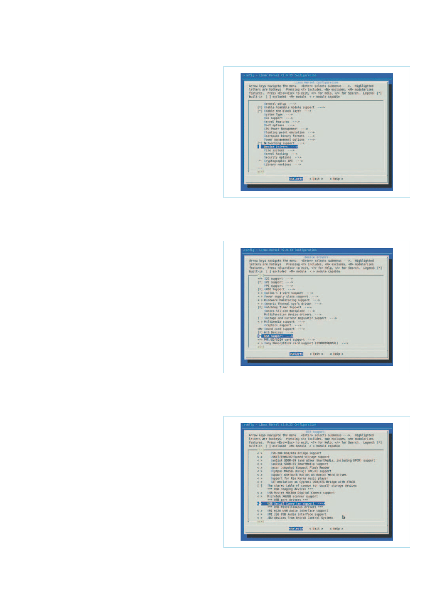
25
elektor 10-2012
eMbedded linux MAde eAsy
•
Test the device.
Enable the driver in the kernel
First switch to the Linux source tree:
cd ElektorLinuxBoardDownload_20120509/
cd linux-2.6.33-lpc313x/
. ./set.h
make menuconfig
In the first step (Figure 5) select the menu item ‘Device drivers’.
Then select ‘USB support’ (Figure 6). With the default configuration
there will be an ‘M’ here instead of the ‘*’ shown in the screenshot.
Use the space bar to cycle through the three options ‘M’ (compile as
module), ‘*’ (compile into kernel), or neither. We select ‘*’ to avoid
the complexity of having to hunt down the module later. The next
menu item is ‘USB serial converter support’ and here also we must
turn the ‘M’ into a ‘*’ (see Figure 7 and Figure 8). Pressing the Enter
key brings up a submenu to select the right driver (Figure 9). Most
readers will probably want to use the FTDI devices or the Silicon
Labs CP210x controllers, and so we set both of these drivers to ‘*’.
To apply these changes, go repeatedly to ‘Exit’ and then, on the last
page, confirm that you want to save a new configuration file.
Compiling the kernel
We can now set off the kernel compilation process.
make zImage
Typical resulting output is shown in Figure 10.
Copy the kernel to the SD card
Put the SD card from the board into an SD card reader and then
connect the reader to the PC. Now copy the kernel to the SD card
as follows
sudo cp arch/arm/boot/zImage /
media/386b3be7-00f3-45e0-832e-1f48c2c3065e/
with, as before, the appropriate change to the long hex string.
When the copy operation is complete unmount the file system
manually in order to ensure that all the blocks are safely written to
the SD card [4]:
umount /media/386b3be7-00f3-45e0-832e-1f48c2c3065e
Check that the driver is available
Now we can boot up the Elektor Linux board as usual. It is impor-
tant to check that JP1 is fitted, so that we force the USB interface to
start up in host mode. We must also make sure that the device is
provided with power over the USB connector from the Linux board.
This is done by fitting J3 in position 3-2.
Figure 5. The 'Device drivers' menu item.
Figure 6. The 'USB support' menu item.
Figure 7. Selecting 'USB serial converter support'
to be built in to the kernel.
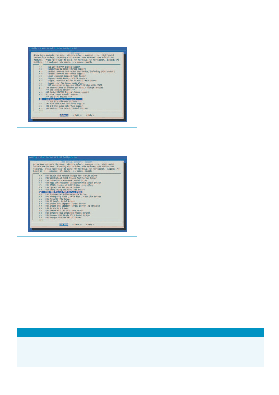
26
10-2012 elektor
Microcontrollers
We can see the first differences during the boot process itself. The
two new drivers make their appearance as follows.
cp210x: v0.09:Silicon Labs CP210x RS232 serial
adaptor driver
USB Serial support registered for FTDI USB Serial
Device
Creating a device file
The command
cat /proc/devices
reveals a new entry ‘188 tty-
USB’. We create a device file with this major number as follows.
mknod /dev/ttyUSB0 c 188 0
Testing the device
If we now plug the USB-to-serial adaptor into the board we get the
following output.
usb 1-1: New USB device found, idVendor=10c4,
idProduct=ea60
usb 1-1: New USB device strings: Mfr=1, Product=2,
SerialNumber=3
usb 1-1: Product: CP2102 USB to UART Bridge
Controller
usb 1-1: Manufacturer: Silicon Labs
usb 1-1: SerialNumber: 0001
cp210x 1-1:1.0: cp210x converter detected
usb 1-1: reset full speed USB device using lpc-ehci
and address 2
usb 1-1: cp210x converter now attached to ttyUSB0
The last line shows that the device file has been correctly created,
and that the kernel has associated the newly-recognised device with
the right device file.
Our Linux operating system includes a small terminal emulator pro-
gram called ‘microcom’. By adding a jumper to bridge the RXD and
TXD lines of the serial port on the USB-to-serial adaptor we can use
this to test the driver. Start up the terminal program using the fol-
lowing parameters.
microcom -s 9600 /dev/ttyUSB0
If you now type characters at the keyboard they will be sent to the
adaptor and then returned to the board. If the driver is working
properly these characters should then be echoed to the screen.
Break the connection between RXD and TXD on the USB-to-serial
adaptor and the characters should no longer be echoed, demon-
strating that the device driver is working. Press control-X to close
Figure 8. Selecting 'USB serial converter support' to be built
as a dynamically-loadable module.
Figure 9. Here we select the USB-to-serial adapter(s)
that will be supported.
Internet Links
[1] sauter@embedded-projects.net
[2] http://en.wikipedia.org/wiki/
Operating_Systems:_Design_and_Implementation
[3] http://en.wikipedia.org/wiki/Process_control_block
[4] www.elektor.com/120180
[5] www.elektor.com/120146
[6] www.gnugeneration.com/mirrors/kernel-api/r4299.html
[7] http://wiki.linuxquestions.org/wiki/Mknod
27
elektor 10-2012
eMbedded linux MAde eAsy
microcom.
In the same way we can modify the kernel to use USB adaptors for
LAN and WLAN, USB sound cards and many other USB devices.
In the next instalment in this series we will look at more devices and
interfaces and test them out with a few simple experiments.
(120181)
Figure 10. Output when compiling the (newly extended) kernel.
Further information at
www.elektor.co
-app
m/
/
//
rf
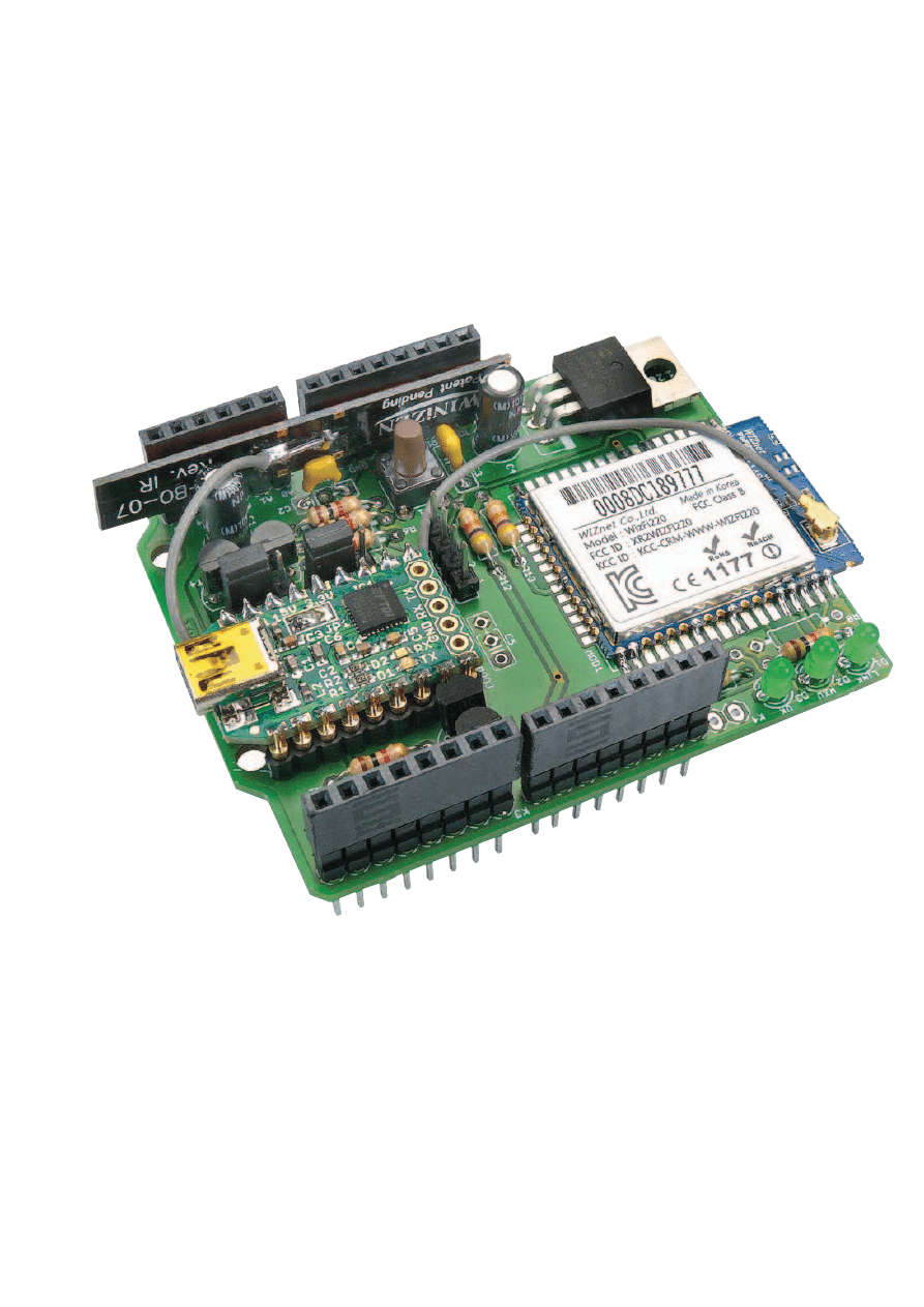
28
10-2012 elektor
MicrocoNTroLLErs
Thou Shalt Communicate!
Wi-Fi/Bluetooth/USB shield
for Platino and Arduino
Today all &
sundry, devices
included, have to
be “connected”, 24/7, all
year round. You may have
a Facebook account, but
what about your oscilloscope?
Does your multimeter tweet
enough? Is your soldering iron
linked in? You may be a non-
communicative nerd but your
bench power supply may be
craving for social interaction.
With the add-on board described
in this article you can hook up
anything to everything, with or
without wires.
Okay, I can’t deny it; I
have a reputation for exagger-
ating. Connecting anything to, errm,
everything is probably a bit over the top. On
the other hand, the board I’m about to pre-
sent in this article is quite versatile. It can
be equipped with a Wi-Fi module allowing
you to connect an electronic device to the
Internet; or with a serial Bluetooth module
it offers wireless connectivity to other serial
Bluetooth capable devices, and a serial-to-
USB bridge enables old-skool wired serial
connectivity.
The board can be used as an add-on board
for microcontroller systems with Arduino-
style extension connectors (Figure 1), like
Elektor’s own Platino [1] (Figure 2), but it
can
also be used
stand-alone as a wire-
less connectivity module for
a PC. Note that you can’t have both
Wi-Fi and Bluetooth modules mounted on
the same board.
About the Wi-Fi module
Wi-Fi modules have been inexpensive, plen-
tiful and easy to find these past few years.
The problem with many of them however
is their manufacturer who refuses to tell
you how to use the module unless you
agree to transfer a substantial amount of
money to the manufacturer’s bank account
in exchange for a few thousand modules
or a customised software library for your
host hardware. Luckily the Korean embed-
ded Internet liberators from WIZnet have
decided to be less secretive about their
products, and sell Wi-Fi modules you can
actually use. I managed to get my hands
on two of their WizFi220 modules, and this
article is the result.
By Clemens Valens
(Elektor UK/INT Editorial)
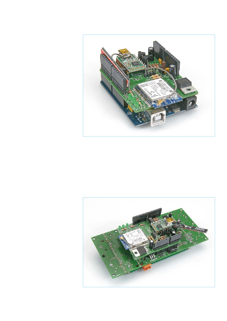
29
elektor 10-2012
Wi-Fi/BLuETooTh/usB shiELd For PLaTiNo aNd arduiNo
The WizFi2x0 modules (there is also a
WizFi210 module) operates with standard
802.11 b/g/n access points at speeds up
to 11 Mbit/s (802.11b), and they support
WEP, WPA, WPA2-PSK and Enterprise secu-
rity standards (802.11i). The modules have
some really cool possibilities. One of them
is the Wi-Fi serial port that’s remarkably
easy to use. Another nice feature is its lim-
ited access point (AP) capability that allows
direct connection to smartphones and tab-
lets like Android-based devices and Apple
gadgets.
T h e W i z F i 2 2 0 m o d u l e m eas u r e s
32 x 23.5 x 3 mm, has an on-board chip
antenna and a Hirose U.FL connector for an
external antenna. The module’s compatible
little brother, the WizFi210, consumes less
power, but cannot provide as much out-
put power and hence has “less range”. 49
connection pads provide enough soldering
points to fix the module on a PCB in such a
way that it will not easily come off. Most of
these pads are probably not useful for unas-
suming users like us, being pitched at high-
volume customers. For the others a simple
two-wire serial connection is available to
transmit and receive data and to configure
the module.
As is often the case with such wireless mod-
ules, the WizFi2x0 can be controlled over a
serial link using AT modem commands (or
Hayes commands). Such commands con-
sist of human-readable strings a few charac-
ters long and starting with ‘AT’. The module
powers on in Command mode so you can
configure it. Once the setup is complete the
module can be switched into Data mode
with the O(nline) command (“ATO”). To
get it out of Data mode back to Command
mode three consecutive ‘+’ characters have
to be send (“+++”).
Design considerations
Some of the configuration commands, like
setting the baud rate of its serial port, are
more or less one-time only, and the mod-
ule remembers these settings. Since the
AT commands are human-readable it may
therefore be practical for the initial setup,
but also for experimenting, to be able to
communicate with the module using a PC
and a serial terminal program. That’s why
I decided to throw in a serial-to-USB con-
verter. Since many Elektor readers may
already have a so-called FTDI serial USB
cable [2], I wanted to be able to use it
with this module. On the other hand, hav-
ing such a converter directly on the board
would also be useful, especially if the host
system does not have a USB serial port,
like Platino. In the September 2011 edition
we presented BOB [3], a very convenient
USB/serial bridge module, and I thought
it was a good idea to add it to my design
too. Now if I could add some clever wiring
it should be possible to connect the USB
converter to either the Wi-Fi module, the
Figure 1. Fully built up Wi-Fi shield on top of an Arduino Uno.
Note the absence of R8 and R10.
Figure 2. Fully built-up Wi-Fi shield on top of Platino,
also equipped with a 20x4 alphanumerical LCD.
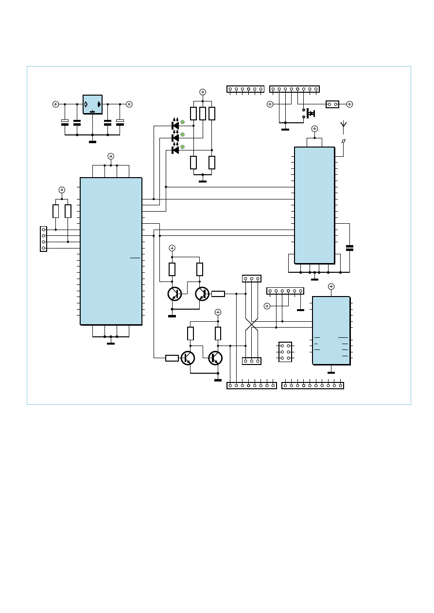
30
10-2012 elektor
MicrocoNTroLLErs
host system or even disconnect it. Flexibil-
ity started creeping into the design.
The Wi-Fi module has to be powered from a
3.3 V rail and it is not 5 V tolerant. The main
objective is to connect the Wi-Fi module’s
serial port to a microcontroller. Such a sys-
tem may run from 3.3 V, but if it is Arduino
or Platino, then the microcontroller runs
from 5 V. Level converters on the serial port
would therefore be necessary. The FTDI
serial USB cable comes in two flavours, 5 V
and 3.3 V, and with level converters both
types would be usable. The BOB was not an
issue because it can handle both levels.
Although the host system may have a 3.3 V
rail, like Arduino, I thought it wise to add
a voltage regulator to the system because
the WizFi220 can consume up to 250 mA in
active mode. As an example, the LP2985-33
voltage regulator on an Arduino Uno board
is specified for 150 mA, which is clearly not
enough. Platino does not have a 3.3 V rail
so this shield could provide it too. A jumper
should allow connection of the 3.3 V as pro-
duced by the shield to the host system.
In this section you can replace all instances
of “Wi-Fi” by “Bluetooth” without having to
change anything else and still have a coher-
ent text. Indeed, many Bluetooth modules
are very similar to the WizFi module: they
can be controlled with AT commands over
a serial link; they run from 3.3 V; they have
similar dimensions and similar require-
ments. It is therefore not very difficult to
add Bluetooth capabilities to the system,
all you have to do is wire a usable Bluetooth
module in parallel with the Wi-Fi module
and that is what I did. I chose the Rayson
BTM220 module because I am at ease with
it [4] and it is very cheap. We have used it
several times in Elektor too. [5][6]
This completes the reasoning that deter-
mined my design. Let’s now have a closer
look at the circuit diagram (Figure 3). If you
SPI_MISO
PCM_SYNC
UART_RTS
UART_CTS
SPI_MOSI
BTM-222
SPI_CLK
SPI_CSB
PCM_OUT
PCM_CLK
UART_RX
UART_TX
USB_DP
USB_DN
PCM_IN
RF_IO
RESET
PIO10
PIO11
AIO0
PVCC
AIO1
PIO0
PIO1
PIO2
PIO3
PIO4
PIO5
PIO6
PIO7
PIO8
PIO9
MOD2
GND
GND GND
VCC
GND GND
GND
17
10
18
37
19
29
38
11
12
13
14
15
16
36
35
34
33
32
20
21
22
23
24
25
26
27
28
30
31
3
1
2
4
5
6
7
8
9
MCP1825S-3302E/AB
IC1
C2
100n
C3
100n
C1
10u
10V
C4
10u
10V
+5V
+3V3
+3V3
UART1_RTS/GPIO27
GPIO21/CLK_11MHZ
GPIO19/CLK_44MHZ
GPIO20/CLK_22MHZ
UART1_CTS/GPIO26
UART0_RTS/GPIO25
UART0_CTS/GPIO24
MSPI_MISO/GPIO6
MSPI_MOSI/GPIO7
MSPI_CLKI/GPIO5
MSPI_CS1/GPIO13
MSPI_CS0/GPIO4
I2C_DATA/GPIO8
UART1_RX/GPIO3
UART1_TX/GPIO2
UART0_TX/GPIO1
UART0_RX/GPIO0
I2C_CLK/GPIO9
PWM0/GPIO10
JTAG_NTRST
DC_DC_CNTL
SSPI_MISO
SSPI_MOSI
EXT_RESET
WizFi220
JTAG_TCK
JTAG_TDO
JTAG_TDI
JTAG_TMS
RTC_OUT1
VOUT_1V8
SSPI_CLK
EXT ANT
VIN_3V3 VIN_1V8
SSPI_CS
ALARM1
GPIO29
ALARM2
GPIO31
GPIO30
GPIO28
VDDIO
MOD1
VBAT
ADC1
ADC2
GND
GND
GND
GND
32
18
31
48
33
34
37
25
46
10
11
12
13
14
15
16
17
19
20
21
22
23
24
26
27
28
29
30
35
36
38
39
40
41
42
43
44
45
47
1
9
2
3
4
5
6
7
8
+3V3
JP4
4
3
2
1
R12
47k
R13
47k
C5
220n
D1
D2
D3
R7
1k
R8
1k
R11
1k
R9
1k
R10
1k
+3V3
T2
BC547B
T1
R2
1k
R1
1k
R3
1k
+3V3
T3
BC547B
T4
R5
1k
R4
1k
R6
1k
+3V3
2x
2x
BOB-FT232R
CBUS4
CBUS3
CBUS2
CBUS1
CBUS0
RESET
MOD3
VCIO
+3V3
TXD
GND
+5V
RXD
CTS
RTS
DCD
DSR
DTR
RI
JP1
1
2 3
JP2
1
2
3
+5V
JP3
1
2
3
4
5
6
K3
1 2 3 4 5 6 7 8
K4
10
1 2 3 4 5 6 7 8 9
K1
1
2
3
4
5
6
7
8
K2
1
2
3
4
5
6
K5
1
2
3
4
5
6
ICSP
120306 - 11
+3V3
S1
+3V3
+5V
+3V3
IOL
IOH
POWER
LINK
RXD
OK
RX_RADIO
TX_RADIO
ASSOCIATED
RX
TX_MCU
RX_MCU
RX_MCU
TX_MCU
TX_FTDI
RX_FTDI
0
2
4
#3
#5
7
#6
8 #9 #10 #11 12 13
GND
AREF
GND
VIN
5V 3V3 RST IOREF
A0
A1
AD
A5 A4 A3 A2
DTR
GND
RXI
CTS
VCC
TXO
SDA
SCL
1
ANT_BT
*
*
*
*
*
JP5
1
2
Figure 3. Complete circuit diagram of the Wi-Fi/Bluetooth/USB shield.
Refer to the text to find out which parts you need for each configuration.
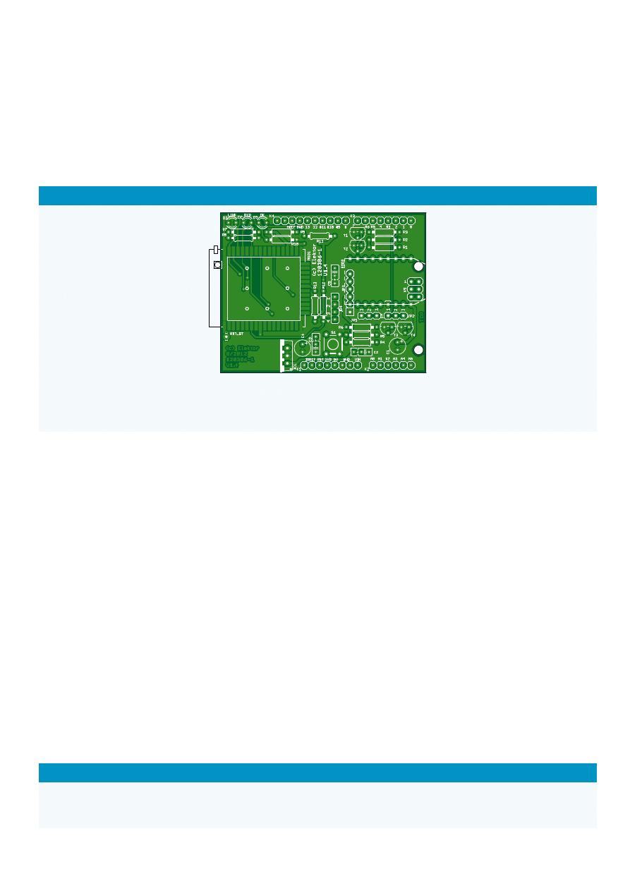
31
elektor 10-2012
Wi-Fi/BLuETooTh/usB shiELd For PLaTiNo aNd arduiNo
have grasped my prose up to here, then the
schematic will have only a few surprises.
Putting it all together
On the left side of figure 3 we have the Wi-Fi
module; on the right side we see the Blue-
tooth module. As you can see they share
the serial RX and TX lines, meaning that
you should not mount both. It is either
Wi-Fi or Bluetooth, never both. The mod-
ules also share two LEDs (D1 and D2); D3
is only used by the Wi-Fi module. A surprise
here may be R8 and R10. Maybe I could have
drawn a better schematic, but I didn’t, so
I have to explain this in writing. It is actu-
ally very simple. The Wi-Fi module sinks the
current for the LEDs whereas the Bluetooth
sources the current. As a result the LEDs
have to be mounted the other way around
as drawn if you use the Bluetooth module.
In that case you should mount R8 and R10
and not mount R7 and R9 (mounting R11
and D3 is useless unless you connect the
LED to a free I/O pin on one of the connec-
tors). For the Wi-Fi module the position of
the LEDs is drawn correctly and you should
not mount R8 and R10 (although nothing
breaks or blows if you do), only R7 and R9
are needed now.
The WizFi module has some pins with spe-
cial functions that you may want to use.
Since I didn’t use them I wired them to a
separate connector JP4. To enable you all
to stack many shields on top of each other
I decided not to wire these signals to the
Arduino extension connectors K1 to K4. If
you need them you can wire them your-
self. Pin 25 (GPIO 21) allows you to restore
the module’s factory defaults. Pulsing it
Low twice will restore the module to Lim-
ited Access Point mode, three pulses will
restore it to Ad-hoc mode. Pin 46 (GPIO 29)
provides a hardware way of switching
between Command (High) and Data
mode (Low). Pin 37 (GPIO 27) is needed
when you want to upgrade the firmware
of the module (probably never). To do so
you have to pull it High. Finally, a low level
on pin 7 (Alarm1) will wake up the module
from deep sleep mode.
The level converters (R1-3, T1-2 and R4-6,
T3-4) are straightforward and have been
used before in Elektor. Transistors T1 and T4
do the level conversion, but invert the sig-
nal at the same time. T2 and T3 correct this.
The resistor values are not critical. I chose to
use as many 1 kΩ resistors as possible.
The RX and TX lines connect to JP1 and JP2.
These 3-pin jumpers may be a bit difficult
to understand at first sight, but when you
follow the lines you should be able to fig-
ure them out. With a jumper on JP1’s pins
1 and 2 the USB serial converter TX pin
is connected to the Wi-Fi (or Bluetooth)
module’s RX input. A jumper on JP2’s pins
2 and 3 connects the USB serial converter
RX pin to the Wi-Fi (or Bluetooth) module’s
TX output. This is the Configure-Module-
With-PC mode. In these positions the USB
serial converter cannot talk to the host MCU
system and it may be better to disconnect
COMPONENT LIST
Resistors
R1–R11 = 1kΩ 5% 0.25W
R12,R13 = 47kΩ 5% 0.25W
Capacitors
C2, C3 = 100nF 50V, 5mm pitch
C5 = 220nF 50V, 5mm pitch
C1, C4 = 10µF 35V, 2.5mm pitch
Semiconductors
D1,D2,D3 = LED, green, 3mm diam.
T1–T4 = BC547C, TO-92 case
IC1 = MCP1825S-3302E/AB, 3.3 V volt-
age regulator, TO-220 case
Miscellaneous
JP1 = 6-pin pinheader, 0.1” pitch,
straight
JP3,JP4 = 3-pin pinheader, 0.1” pitch, straight,
w. 2 jumpers
JP2 = 4-pin pinheader, 0.1” pitch, straight
K1,K3, K4 = 8-pin stackable header, 0.1” pitch,
vertical
K2 = 6-pin stackable header, 0.1” pitch,
vertical
K5 = 6-pin (2x3) stackable header, 0.1”
pitch, vertical
S1 = pushbutton, SPNO, through-hole,
6x6mm
Mod3 = BOB-FT232R USB-to-Serial
Bridge, Elektor Shop # 110553-91, or
USB-to-Serial cable, Elektor Shop #
080213-71 (5 V) or # 080213-71 (3.3 V)
Mod2 = Rayson BTM22x Bluetooth
module
Mod1 = WIZnet WizFi2x0 Wi-Fi module
PCB # 120306-1 [1]
Elektor Projects & Products
•Platino, a versatile board for AVR microcontroller circuits (October 2011); PCB # 100892-1 from Elektor Shop
•BOB-FT232R USB-to-Serial Bridge (September 2011); module, Elektor Shop # 110553-91
•USB-to-TTL Serial Cable (June 2008); cable, Elektor Shop # 080213-71 (5 V) or # 080213-71 (3.3 V)

32
10-2012 elektor
MicrocoNTroLLErs
the board from the host system. The board
will be powered from the USB port.
If you put a jumper on JP1’s pins 2 and 3
and on JP2’s pins 1 and 2 the USB serial con-
verter can be used to talk to the host sys-
tem. In this case you should not mount the
wireless module (or the level converters) as
this kind of communication may disturb it.
This is the USB-Shield mode.
Not installing any jumpers will put the
board in Wireless mode and the USB serial
converter has no use. However, you could
leave it on and wire it to other pins on the
extension connectors. This is for instance
useful in an Arduino-with-software-UART
configuration or in a host system with more
than one UART.
Finally some remarks on details. The Reset
button is mainly intended for Platino which
doesn’t have one. It is also useful when the
Arduino reset button becomes inaccessible
because of the shield mounted on top of
it. This depends on the Arduino board and
its revision.
K5 is not connected. I only put it on the
board to provide access to its signals if the
host is Arduino.
Turning practical
To turn a circuit diagram into a real shield
or extension board a printed circuit board
(PCB) is needed. I designed one and you can
download the Eagle CAD files from the web
page that accompanies this article [7]. The
PCB is the size of an Arduino Uno except that
it is a rectangle without the funny-shaped
short side of an Arduino Uno. All the compo-
nents are through-hole types; only the Wi-Fi
and Bluetooth modules have surface mount
footprints. JP5 and the Bluetooth module are
located on the solder side of the board; the
other components should go on the compo-
nent side. Note that if you use non-stackable
connectors for K1 to K4 you should mount
them on the solder side if you want to stick
the board on an Arduino or Platino.
JP1 and JP2 are positioned in such a way that
the jumpers should always be in the same
position, i.e. both to the left, both to the
right or both absent. Actually, you could
leave a jumper on JP2 in case you wanted to
listen in on the MCU wireless module com-
munications. This can be useful for debug-
ging purposes.
JP3 has a few contacts in common with the
BOB serial-to-USB bridge, the idea being
that you use either a BOB or an FTDI cable,
not both.
For full 3.3 V systems the level converters
and voltage regulator can be left off. In this
case you have to place two bypasses (wire
bridges) from R3-JP1 to R2-T2 and from
R6-MOD1 to R5-T3. Resistors R3 & R2 and
R5 & R6 are positioned in such a way that
the wire bridges are very easy to install and
Listing 1.
Example of setting up the WizFi2x0 module as a serial server using AT commands. The commands are in boldface, the module’s responses
are in italic. Comments appear in brackets (). See the WizFi2x0 user manual for more commands.
AT (wake up)
[OK]
AT+NSTAT=? (what is your status?)
MAC=00:08:dc:18:97:76
WSTATE=NOT CONNECTED MODE=NONE
BSSID=00:00:00:00:00:00 SSID=”” CHANNEL=NONE SECURITY=NONE RSSI=0
IP addr=0.0.0.0 SubNet=0.0.0.0 Gateway=0.0.0.0 DNS1=0.0.0.0 DNS2=0.0.0.0
RxCount=0 TxCount=0
[OK]
AT+WPAPSK=germaine,”Philippe Noirette” (set SSID & pass phrase)
Computing PSK from SSID and PassPhrase...
[OK]
AT+NDHCP=1 (request IP number from DHCP server)
[OK]
AT+WAUTO=0,germaine (automatically connect to germaine)
[OK]
AT+NAUTO=1,1,,8011 (setup for auto connect: server, TCP, port 8011)
[OK]
ATA (start auto connect)
IP SubNet Gateway
192.168.2.7: 255.255.255.0: 192.168.2.1
[OK]
(now you can connect (telnet) to the module over Wi-Fi)
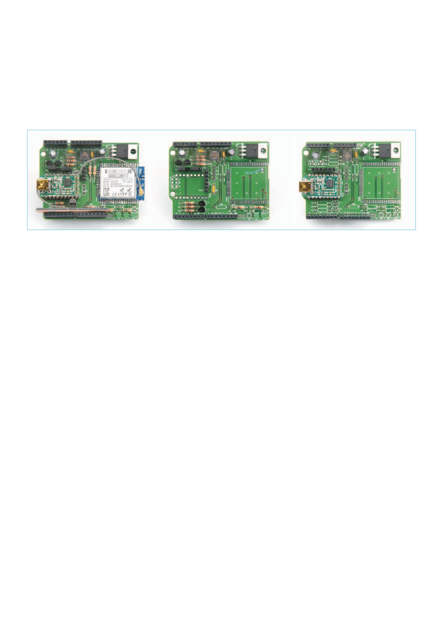
33
elektor 10-2012
Wi-Fi/BLuETooTh/usB shiELd For PLaTiNo aNd arduiNo
span only minimum distance. You will also
have to short JP5 on the solder side of the
board.
As mentioned before, the orientation of the
LEDs depends on the wireless module. The
component print on the PCB corresponds
to the Wi-Fi module. If you mount a Blue-
tooth module you should mount the LEDs
D1 and D2 ‘the wrong way around’. Also,
only mount R7 or R8 and R9 or R10.
The 3.3 V voltage regulator can be installed
lying on his back or standing up.
Three main configurations are possible (Fig-
ure 4), but you may have a need for other
variants:
•
Wi-Fi shield — no need for the BOB if
you own an FTDI cable, although you
can always install one. JP3 is available
for connecting the FTDI cable. Mount all
LEDs as indicated on the PCB and do not
mount R8 nor R10. Level converters will
be needed and the 3.3 V voltage regu-
lator probably too, depending on your
host system.
•
Bluetooth shield — similar as the Wi-Fi
shield except for the LEDs. D3 has no
function and you should not mount R7
and R9 but mount R8 and R10 instead.
As an antenna you can use a piece of
(insulated) wire of 31 mm long.
•
Serial-to-USB bridge shield — just the
BOB without level converters. Do not
forget to put a drop of solder on JP1 of
the BOB to configure it for 5 V or 3.3 V
operation. Add 3.3 V voltage regula-
tor and reset push button to taste. The
LEDs can be useful too, but you will have
to wire them to a connector pin. You
should short pins 2 and 3 of JP1 and pins
1 and 2 of JP2 with a jumper or a wire
bridge.
Testing
In case of the Wi-Fi or Bluetooth configura-
tions connect the board to a USB port on the
PC using an FTDI serial converter cable or the
BOB serial-to-USB bridge. Figure out which
COM port was created by the operating sys-
tem (OS) of your PC (make sure you have the
appropriate drivers for your OS installed. If
you haven’t you can get them, including the
necessary documentation, at
www.ftdi-
chip.com
) and start a serial terminal pro-
gram. The WizFi220 module has a default
baud rate of 115 200 bits/s, for the BTM220
module this value is 19 200. Both modules
use 8 bits, no parity and no hardware flow
control. In the terminal type ‘AT’ followed
by the Enter key. If you set up everything the
right way the module should respond with
‘[OK]’ or ‘OK’. If this test succeeds you’re
in business. Refer to Listing 1 for a working
Wi-Fi example (don’t forget to adapt the
SSID and pass phrase to your network).
For a BOB serial-to-USB bridge configura-
tion the steps are more or less the same
except that there is no point in punching in
AT commands in the terminal unless your
host system responds to these. It is up to
you to provide a host that can communicate
over a serial link.
Thanks go out to Joachim Wulbeck of WIZnet
Europe GmbH (www.wiznet.eu) for providing
the WizFi220 modules and the Wi-Fi antennas.
(120306-i)
Internet Links and References
[1] Platino: www.elektor.com/100892
[2] USB-to-TTL serial cable:
www.elektor.com/080213
[3] BOB serial-to-USB bridge:
www.elektor.com/110553
[4] Experiments with Rayson Bluetooth
modules:
http://elektorembedded.blogspot.
com/2010/08/rayson-btm222-btm112-
bluetooth-modules.html
[5] Bluetooth with the ATM18:
www.elektor.com/080948
[6] Bluetooth for OBD-2:
www.elektor.com/090918
[7] Wi-Fi shield: www.elektor.com/120306
[8] Wi-Fi shield on Elektor Projects:
http://www.elektor-projects.com/pro-
ject/wi-fi-bluetooth-usb-shield-for-ardui-
no-platino.12252.html
Figure 4. The three main configurations next to each other. The Bluetooth module is not visible (middle board) because it is mounted on
the other side of the PCB. Note that this is an early revision of the PCB that has the same shape as an Arduino Uno board. The final PCB is
rectangular.
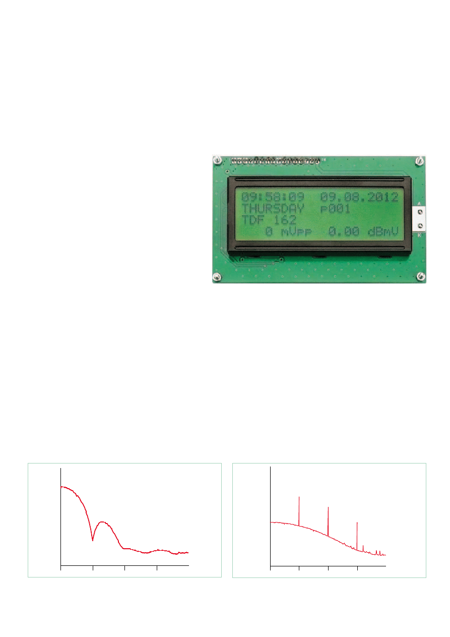
34
10-2012 elektor
radio
AVR Software Defined Radio (6)
decoding options for
BBC 198 kHz data signals
By Martin Ossmann (Germany)
This series has demonstrated that the ever-
popular AVR controllers are also useful for
signal processing. In this final instalment we
take a closer look at a few more decoding
methods. As usual we like to back up the
theory with some practice: This instalment
shows how to extract time-of-day information
from BBC AM broadcasts.
In the last instalment of this series [5] we demonstrated the decod-
ing of time-signal transmissions. Using the described digital IIR and
matched CIC filter it is possible to receive and decode time signals
sent by the German DCF77, the UK MSF and French TDF162 stations.
In this instalment we go on to decode the digital information trans-
mitted by the BBC on long wave at 198 KHz (Droitwich) and also the
recently discontinued medium wave 648 KHz service. To this aim we
look at alternative decoding strategies and demonstrate how they
can be implemented.
Bit-clock synchronisation
In the world of communications technology there are many meth-
ods by which synchronous data can be sent through the ether. Here
a digital data stream runs continuously through the communication
system at a defined clock rate. At the receiver the signal often first
undergoes demodulation. The resultant signal is then a sequence
of data bits which contain the transmitted information.
For this experiment to achieve bit-clock synchronisation with the
receive data it will be necessary to use a simple radio front-end (or
the receiver board available from the Elektor shop), the receiver
software ‘EXP-RX-FM-125kHz-RDSlike-BitSync-V01.c’, a signal gen-
erator with a 125 kHz series resonant circuit and the transmitter
software ‘EXP-TX-FM-125kHz-RDSlike-V01.c’. This last program
generates frequency modulated digital data at 125 kHz with a data
rate of 31.25 bit/s. The data stream and bit clock are output from
the D/A converter outputs.
At the receiver site the signal is sampled at a frequency of
31.25 Hz x 16 = 500 Hz
to recover the clock. Each bit is therefore sampled 16 times. You
could try to reconstruct the 31.25 KHz bit clock from the received
31.25Hz
Figure 1. Frequency spectrum of the 31.25 Hz data signal.
31.25 Hz
Figure 2. The spectrum of the rectified data signal.
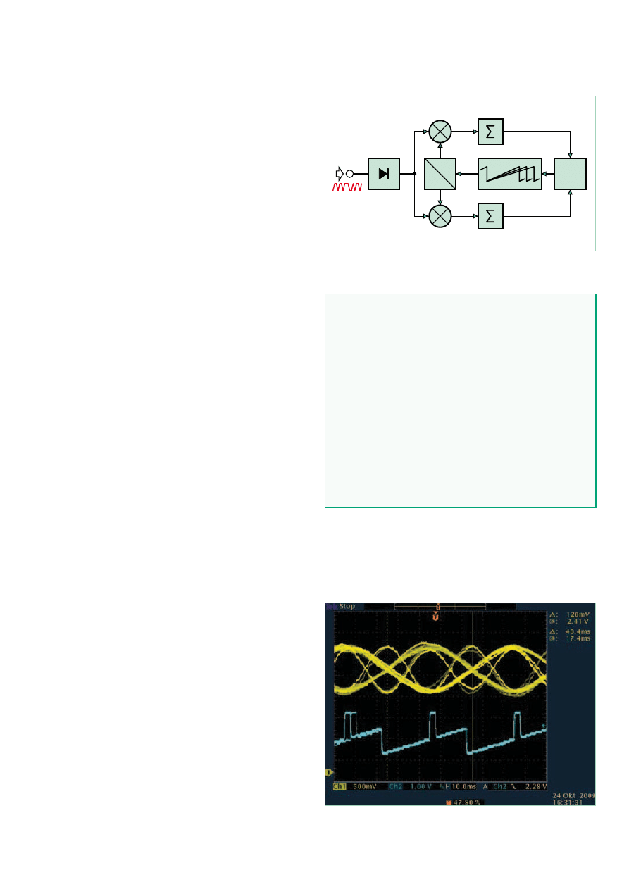
35
elektor 10-2012
aVr Software defined radio
data signal by using a PLL (phase locked loop). Unfortunately it is
not quite so simple. The reason becomes clear when you look at the
received signal spectrum given in Figure 1. There is in fact no signal
component at 31.25 Hz for a PLL to lock onto.
Once the data signal has been rectified however, its spectrum (Fig-
ure 2) now shows a component at 31.25 Hz. A PLL will now be able
to lock onto the signal. The principle of the data recovery PLL is out-
lined in Figure 3.
This PLL is in fact similar to the design used in an earlier instalment
of this series to recover the carrier frequency (see Figure 7 in the
fourth instalment of this series [4]). With reference to the ‘EXP-RX-
FM-125kHz-RDSlike-BitSync-V01.c’ program the bit-clock frequency
is controlled in the following manner: The do-Signal-Sample() rou-
tine in Listing 1 is called at 16 times the bit clock rate. In this routine
the variable Clk16 is incremented or reset to zero when it reaches
16. The phase of the saw-tooth signal is regulated so that the centre
of the ramp (Clk16 = 8) is coincident with the centre of the transmit-
ted bit. The bit value is evaluated and processed in the routine doBit-
Sample(). Phase adjustment is performed in the following manner;
in the normal case Clk16 is incremented to 16 and then reset by the
digital signal clock. Now depending on the sign of the output from
the phase comparator this value can be changed to either 15 or 17
to provide some phase adjustment.
In order to correctly control the clock PLL it is necessary to output
the demodulated signal at the output of DAC1. Clk16 with Peak
at Clk16 = 8 (i.e. at the sampling instant) is output from DAC2.
Figure 4 shows the reception of BBC Radio 4 at 198 KHz LW (see
Figure 5).
Early-Late Synchroniser
In addition to the conventional PLL a so-called ‘Early-Late’ synchron-
iser can be used to recover the clock signal. The eye-diagram shown
in Figure 6 helps explain how this technique works.
Again it is necessary for the Clk16 signal to synchronise with the
bit clock so that the data signal is sampled in the centre of the bit.
In order for this to be achieved the signal is sampled at the early
time E and the late time L. This can be performed, for example on
the third (E) and twelfth (L) clock of the Clk16 clock. When both
of these measured values are the same amplitude then we can be
confident that E and L are centred about the mid point. When on
average one set of the values is greater than the other it indicates
that the eye has shifted from its optimal point and phase of Clk16
requires some correction.
The program code corresponding to this process in given in List-
ing 2. Ten samples of the E (early) and L (late) values are summed to
produce the value ‘earlyLateDelta’. This value is then used to correct
the Clk16 period. The code for this synchroniser can be tested with
the ‘EXP-RX-FM-125kHz-RDSlike-BitSync-V01.c’ program.
Decoding the phase modulated BBC198 signal
Now we come to a practical application of bit synchronisation when
we program the receiver to recover the phase-modulated data sent
out by the BBC as part of its Radio 4 LW broadcast on 198 kHz.
Details of the transmitted signal are given in the BBC publication
[7]. Data is sent by modulating the 198 KHz carrier phase by ±22.5°.
The data rate achieved is 25 bit/s using Manchester coding (also
known as bi-phase coding) with filtering. Using this type of modula-
tion ensures that the average phase deviation always sums to zero
U
Data
I channel
V
Q channel
cos
sin
Cordic
CLOCK oscillator
Figure 3. The clock-PLL principle.
Figure 4. Eye diagram of the BBC198 signal.
Listing 1: Phase adjustment
void advanceCLK16() {
Clk16++ ;
if ( Clk16 >= ClockPeriod ) { Clk16=0 ; }
}
void doSignalSample(){
int16_t Signal ;
ATOMIC_BLOCK(ATOMIC_FORCEON) {
Signal=FRQcicout ;
}
ClockPLL16(Signal) ;
doBitSample(Signal) ;
advanceCLK16() ;
}
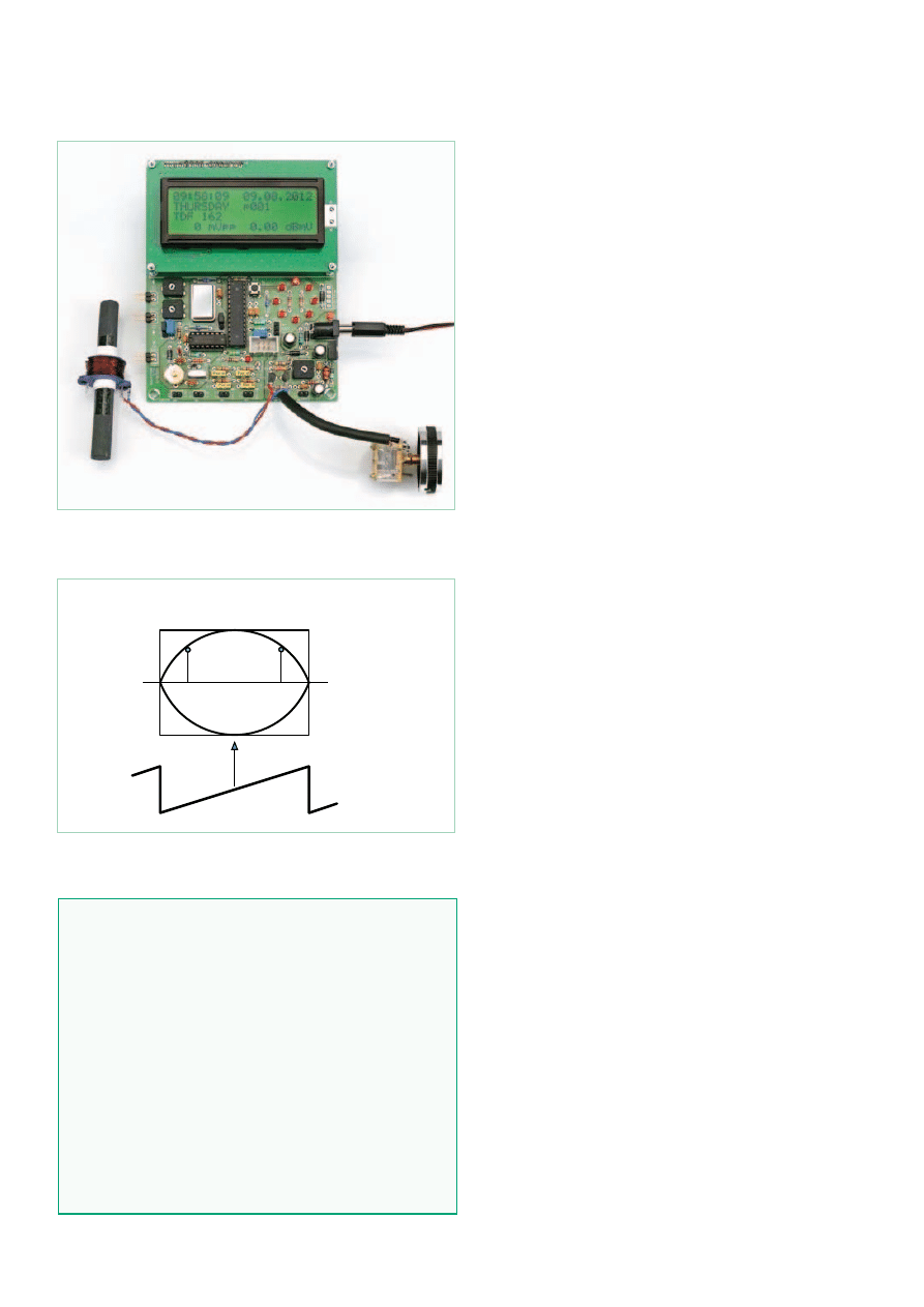
36
10-2012 elektor
radio
so (as before the modulation was introduced) the carrier can still be
used as a highly stable frequency reference.
The A/D converter uses a clock equal to
20 MHz / 2,500 = 8 kHz.
At this sampling rate the 198 kHz carrier is mixed down to
198 kHz – (25 x 8 kHz) = –2kHz.
The ‘intermediate frequency’ is therefore –2 kHz and is sampled at
four samples per period in the same way as in the IQ sampling mixer
earlier. The negative sign indicates that the mirrored sideband is
used. After separation into the I and Q components both are first
passed through second-order CIC filters and downsampled with an
M
d
factor = 16. Next in line is another low-pass CIC but this time
without downsampling. Instantaneous values of amplitude and
phase values are now produced from these filtered I and Q signals
processed using the CORDIC process.
One possibility for signal demodulation is to use a PLL to recover the
carrier and then decode the NRZ (Non Return to Zero) signal. Here
it refers to the original data signal which has been used to phase
modulate a carrier and which will be recovered in the receiver. For
decoding however the use of a PLL control loop which interprets a
phase modulation as a frequency modulation is not necessary. The
conversion is shown in Figure 7.
The theoretical NRZ-phase response is represented as a signal
response p(t). To reduce the signal bandwidth phase changes occur
only slowly. The actual phase response is more like the signal q(t).
The sampling rate for the demodulated signal is 400 Hz so each bit
is sampled 16 times. Now according to communication theory fre-
quency is the rate of change of phase. The frequency response f(t) is
given by the derivative of q(t) with time. When the phase increases
linearly with time there is a constant positive frequency. When the
phase decreases linearly with time there will be a constant nega-
tive frequency.
Using additional low pass filtering the signal g(t) is recovered from
f(t) and can now be readily evaluated. The data stream is sampled
mid-bit to determine its value. When the value is positive it is inter-
preted as a ‘1’ and when negative as a ‘0’. Application of the CORDIC
algorithm produces phase samples to give the instantaneous fre-
quency. These are again low-pass filtered with a CIC filter to produce
the signal g(t). This signal in turn supplies the bit-clock recovery.
This results in the waveform shown in Figure 8 in the second instal-
ment of this series [2].
With more processing the blocks of data are identified and decoded.
How this functions will be explained later on. For now Listing 3
shows a data sample received from the BBC 198 kHz signal.
Block Synchronisation
Once the data bit stream has been recovered from the receive signal
the final task is to identify the beginning and end of the data packet.
This process is known as block synchronisation.
The majority of radio traffic systems use blocks of data of fixed
Signal
Eyepattern
CLK16
E
L
Figure 5. The complete receiver for reception of BBC198.
Figure 6. Eye diagram of the early-late synchroniser.
Listing 2: Early-Late Synchroniser
void earlyLateSynchronizer(int16_t Signal){
if ( Clk16==3 ) { earlyValue=abs(Signal) ; }
if ( Clk16==12 ) { lateValue=abs(Signal) ; }
if ( Clk16==8 ) {
earlyLateDelta += lateValue-earlyValue;
ClkCnt++ ;
ClockPeriod=16 ;
if (ClkCnt==10){
ClockPeriod += earlyLateDelta/16 ;
earlyLateDelta=0 ;
ClkCnt=0 ;
}
}
}
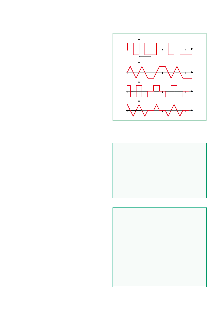
37
elektor 10-2012
aVr Software defined radio
length. When the receiver is first switched on it is necessary to
determine where the beginning of each block occurs in the data
stream. There are several commonly used techniques to identify
data start; one method is to use a unique sequence of bits to form a
preamble. This sequence is never allowed to occur in the data field.
RFID tags of the type EM4102 use this method. This preamble occu-
pies space in the data stream and therefore, to some extent reduces
the available channel data bandwidth. Many communication sys-
tems use the information contained in the data for error correction
field as the block boundary marker.
Error detection
Many data communication systems use a checksum added to the
end of each block of data which allows the receiver to detect data
corruption and also to correct the error. It can be shown that this
additional information can also be used to perform block synchro-
nisation. First we will describe how the checksum is calculated using
the 125 KHz test transmitter together the ‘EXP-TX-FM-125kHz-
RDSlike-V01.c’ program. The calculation software is given in List-
ing 4 and the CRC hardware generator block diagram is shown in
Figure 8.
Ten CRC check bits are calculated using a shift register with XOR
gated feedback taps. The 16 data bits are clocked through a shift
register and control the new bits which end up in the syndrome shift
register. The CRC checksum is produced after 16 clock periods cor-
responding to the 16 data bits. A hex value of 198H is added to the
checksum using the XOR function which simplifies the synchroni-
sation process at the receiver site. The 10 check bits are sent after
the 16 data bits. This technique is very similar to the standard RDS
system described in [8].
When the receiver knows where a new block starts it computes the
syndrome (in exactly the same way as the transmitter) of the fol-
lowing 16 data bits and compares it with the 10 CRC bits follow-
ing the data. In order to find the start of the block it is necessary
to check each time a new bit is received whether the previous 26
bits produced an error-free combination of 16 data bits and 10
checksum bits. This test produces an ‘OK’ at a spacing of 26 bits
while receiving a continuous data stream. Occasionally an ‘OK’ will
occur in an incorrect position. The block synchronisation algorithm
looks for a pattern with three ‘OK’ signals spaced by 26 bits. When
this is detected it assumes that the block start has been correctly
identified.
Figure 9 shows schematically how the check bits are continuously
calculated. The syndrome calculator can be looked on as a type of
filtering. The feedback shift register is configured in the same way
as the one used in the transmitter path. The continuous stream of
bits are processed and as each bit emerges from the 10+16 bit shift
register it is taken into account in the syndrome shift register. The
software need only check if the syndrome shift register contains
the value 198H which was the value added during encoding at the
transmitter end. When this value is found the software responds
with an ‘OK’. A counter called ‘localTime’ is incremented from zero
to 25. A value of zero indicates that a complete block together with
the check bits have been processed.
Periode T
q(t)
p(t)
f(t)
g(t)
0
0
1
0
0
0
0
1
0
0
Figure 7. Phase modulation as frequency modulation.
Listing 3: BBC 198 kHz signal: receive Data
+E EB11 0391
+0 AAAA AAAA
+E E8F1 0391
+E EB09 0391
+E EB49 0391
+0 AAAA AAAA
+E EB31 0391
+E EB41 0391
+0 5475 2980 time= 18:38 week=07 day=02 tuesday
+E EB29 0391
Listing 4: Transmitter CRC calculation
SendBits(w,16) ;
Syndrom=0 ;
for (j=0 ; j<16 ; j++) {
Syndrom=Syndrom<<1 ; // outgoing bit is at mask
0x0400
if (w & 0x8000) {
Syndrom ^= 0x0400 ; // xor into outgoing bit
}
w=w<<1 ;
if ( Syndrom & 0x0400 ) {
Syndrom ^= 0x1B9 ;
}
} ;
Syndrom=(Syndrom^ofs)<<6 ;
SendBits(Syndrom,10) ;
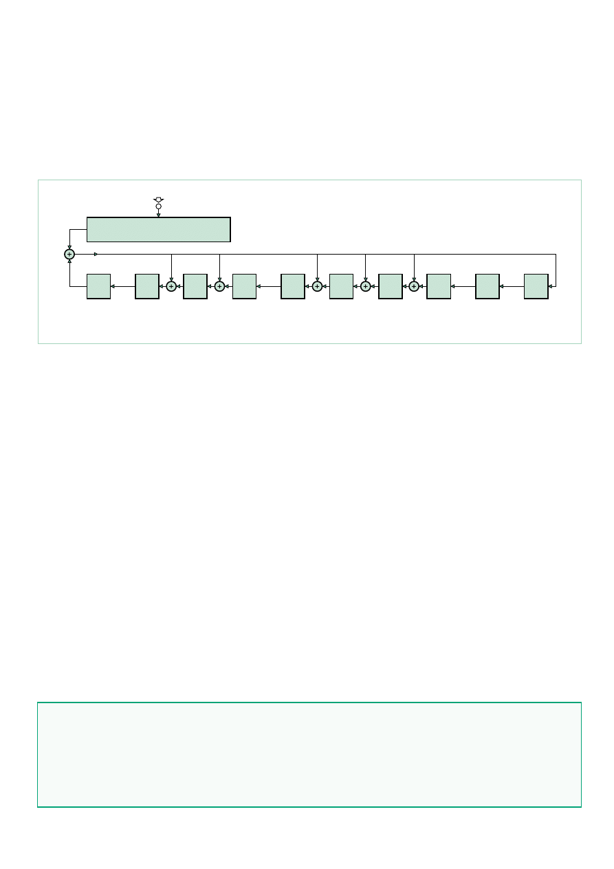
38
10-2012 elektor
radio
To demonstrate this behaviour, a variant of the receiver was pro-
grammed so that the actual time (localTime) is output as a saw-
tooth waveform from the PWM-DAC output. The second PWM
DAC output will be high when the synchronisation circuit detects
an ‘OK’. The repetitive waveform can be seen in Figure 10. Also vis-
ible is a position where a false ‘OK’ is detected. It is may be neces-
sary to wait a little before this random event happens.
After synchronisation when the ‘OK’ occurs at the time interval zero
it indicates that error-free block has been received and the data can
be output. With this the data reception process is complete.
This description of synchronisation applies for the BBC long wave
transmission on 198 kHz. The data sent by the BBC does not how-
ever contain RDS parameters but uses blocks of data containing 47
data bits with a 13-bit checksum. The data is described in detail in
the documentation [7] and is relatively easy to extract. In particu-
lar, for simplicity the time-of-day information is simply coded in one
complete block.
BBC648 AMSS reception and decoding
This last exercise was intended to demonstrate data reception
from the European World Service signal which the BBC transmits
on 648 KHz. In the mean time due to budget cuts transmission on
this frequency has sadly been discontinued. It is however instruc-
tional to demonstrate how the AMSS data is decoded in this case.
Up until recently the BBC sent low frequency AMSS data as part of
its 648 kHz AM transmission (see the associated literature [10]). The
front end of our receiver samples at 20 MHz / 1,875 = 10,666... kHz.
This results in an intermediate frequency of:
648 kHz – 61 x 10,666... kHz = -2,666... kHz = 0.25 x 10,666... kHz.
Bi-phase signalling is used with a phase modulation of ±20°.
With regard to the modulation and bit-coding method used by the
data traffic it is (almost) identical to 198 KHz system described ear-
lier. The difference here is that each block consists of 36 message
bits and 11 CRC check bits. Two blocks form a group and a defined
number of groups form a DRM-SDC block. A complete description
of all the features is available in the DRM specification. Our simple
receiver only extracts and displays the name of the transmitter sta-
tion but is, never the less, a fully functioning data receiver.
Listing 5 shows the receive data. The output ‘2/7+’ indicates that
the second group from seven has been received with no detected
errors. The data is decoded when all seven groups have been
received.
And finally…
This now brings to a close the six-part series on signal processing
and ‘Software Defined Radio’ using AVR microcontrollers. It has
powerfully demonstrated just what can be achieved with even rel-
atively modest microcontrollers. Commercial SDR receivers employ
X
9
16-bit data register parallel-in, serial-out
Data (16 bits)
X
8
0x01B9 = 0b000110111001
= 9876543210
g(x) = x
^
10 + x
^
8 + x
^
7 + x
^
5 + x
^
4 + x
^
3 + x
^
0
X
7
X
6
X
5
X
4
X
3
X
2
X
1
X
0
__
Figure 8. CRC1.
Listing 5: BBC 648 kHz signal: AMSS SDC data
[6 1]BBC WS [C B] [6 B] 0/7+ 1/7+ 2/7+ 3/7+ 4/7+ 5/7+ 6/7+ 7/7+!0007 ;
[6 1]BBC WS [C B] [6 B] 0/7+ 1/7+ 2/7+ 3/7+ 4/7+ 5/7+ 6/7+ 7/7+!0007 ;
[6 1]BBC WS [C B] [6 B] 0/7+ 1/7+ 2/7+ 3/7+ 4/7+ 5/7+ 6/7+ 7/7+!0007 ;
[6 1]BBC WS [C B] [6 B] 0/7+ 1/7+ 2/7+ 3/7+ 4/7+ 5/7+ 6/7+ 7/7+!0007 ;
[6 1]BBC WS [C B] [6 B] 0/7+ 1/7+ 2/7+ 3/7+ 4/7+ 5/7+ 6/7+ 7/7+!0007 ;
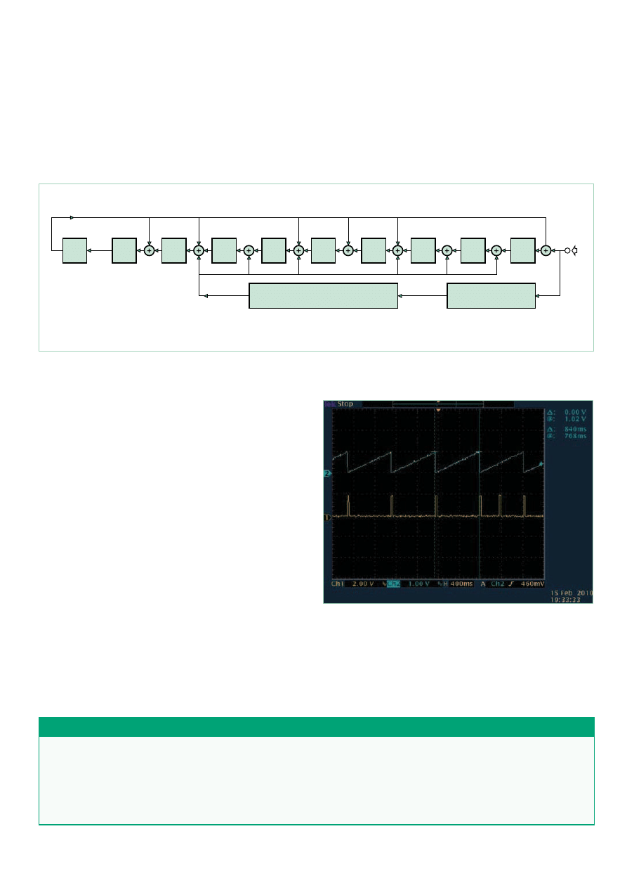
39
elektor 10-2012
aVr Software defined radio
exactly the same techniques as detailed here; the only difference
is that they use more powerful DSPs and radio front-ends which of
course also makes them correspondingly more expensive!
(120392)
Internet Links
[1]
www.elektor.com/100180
[2]
www.elektor.com/100181
[3]
www.elektor.com/100182
[4]
www.elektor.com/120088
[5]
www.elektor.com/120089
[6]
www.elektor.com/120392
[7]
http://downloads.bbc.co.uk/rd/pubs/reports/1984-19.pdf
[8]
ftp://ftp.rds.org.uk/pub/acrobat/rbds1998.pdf
[9]
www.drm.org/
[10]
www.ebu.ch/fr/technical/trev/trev_305-murphy.pdf
www.broadcastpapers.com/whitepa-
pers/ABUBBCamss2006.pdf?CFID=1
6508900&CFTOKEN=dac28b1a87e5
4d77-47F9A337-9A30-F5E3-667FAB2A9EA27223
X
9
16 data bits
10 check bits
Serial
Data In
X
8
0x01B9 = 0b000110111001
= 9876543210
g(x) = x
^
10 + x
^
8 + x
^
7 + x
^
5 + x
^
4 + x
^
3 + x
^
0
X
7
X
6
X
5
X
4
X
3
X
2
X
1
X
0
__
X
^
26 = 0b000110111001
= 9876543210
__
Figure 9. CRC2.
Figure 10. The OK signal.
Elektor products and support
•Signal generator (Kit with PCB and all components, # 100180-71)
•Universal receiver (Kit with PCB and all components, # 100181-71)
•Active ferrite antenna (Kit with PCB and all components, #
100182-71)
•Combi-kit with all three components plus USB/TTL converter BOB
FT232: # 100182-72
•USB/TTL converter BOB FT232, fully populated and tested, #
110553-91
•Free software downloads (hex files and source code)
All of these products and downloads are available through the web
page: www.elektor.com/120392
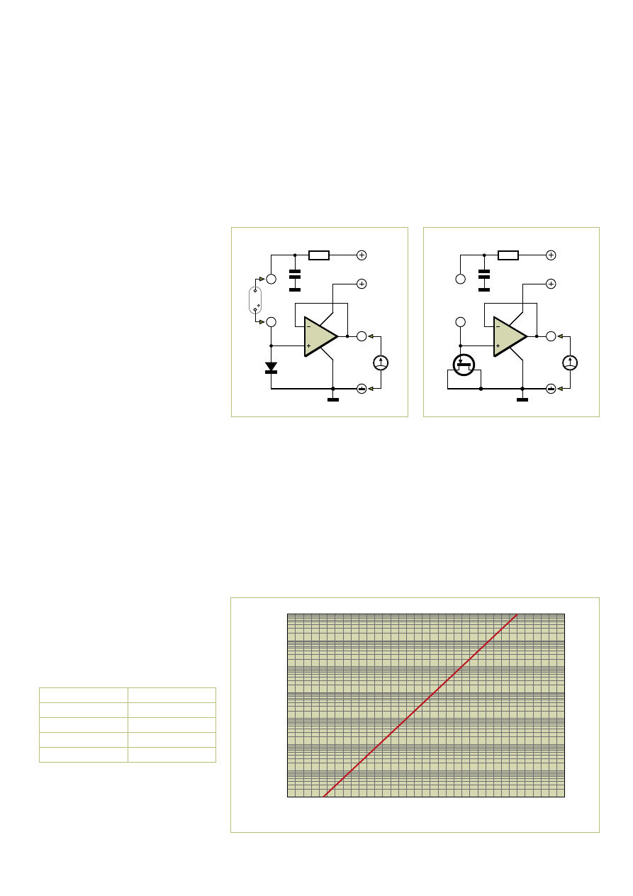
40
10-2012 elektor
test & measurement
Picoammeter
The instrument described here can be used
to measure currents from around 0.1 pA to
1 µA, without the need to change range.
One approach is to exploit the logarithmic
characteristic curve of a silicon diode, with
the diode voltage buffered by a type TLC272
CMOS opamp. For the first experiment we
used a 1N4148 silicon diode (see l/h circuit).
However, the lowest current measurable
using this arrangement was over 10 pA, as
below that value the diode’s characteristics
deviate from the logarithmic curve.
A particularly good diode with a very low
reverse current is the gate-source diode
inside a BF245 JFET (see lower circuit).
Using this we can measure currents of less
than 1 pA. To calibrate the circuit we use
known currents at the input and measure
the output voltage:
1 µA
580 mV
100 nA
510 mV
10 nA
440 mV
1 nA
370 mV
100 pA
300 mV
The above values closely follow a
logarithmic curve: each increase in current
by a factor of ten gives an output voltage
increment of 70 mV. We have already
covered four decades: the graph shows how
the curve can be extended to even lower
currents.
Experiments show that it is even possible to
get useful results with currents of less than
1 pA. In this case, however, it is essential to
carefully screen the whole circuit, including
the item under test, against the effects of
external fields. For the prototype a metal tin
was used with feed-throughs.
Some results obtained with the prototype:
•ionisation chamber with a sample of
pitchblende: about 1 pA;
•BPW34 photodiode used as a radiation
detector (in complete darkness): about
10 pA;
•burnt-out filament lamp: about 100 pA;
•burnt-out halogen lamp: about 0.1 pA.
From these last two results we can see
that quartz glass is a considerably better
insulator than ordinary glass.
(120322)
By Burkhard Kainka (Germany)
IC1.A
TLC272
+ 9V
R1
1M
0...+ 40V
C1
100n
D1
1N4148
M1
V
120322 - 11
IC1.A
TLC272
+ 9V
R1
1M
0...+ 40V
C1
100n
M1
V
0,1pA...1uA
100...600mV
T1
BF245
120322 - 12
1000000
100000
10000
1000
100
10
1
0
100
200
300
400
500
600
700
120322 - 13
0.1
I
[pA]
U
[mV]
It is often necessary to deal with
tiny currents in the picoamp to
microamp range when making
measurements in ionisation
chambers and other radiation
sensors, as well as when testing
insulation.

the world needs
innovative
electronics.
they are
on display here.
Tickets & Registration:
www.
e
lectronica.de/en/2012
25th International Trade Fair
for Electronic Components,
Systems and Applications
Messe München
November 13–16, 2012
www.
e
lectronica.de
PicoScope 3406B
200 MHz bandwidth
128 MS deep memory
1 GS/s real-time sampling
Advanced digital triggering
200 MHz spectrum analyzer
Function generator and AWG
Spectrum analyzer.
Full SDK and advanced triggers
Serial decoding
(CAN, FlexRay, LIN, SPI, I
2
C, UART)
Mask limit testing,
measurements and math channels
Colour persistence modes,
all as standard and free updates
ENTER
ONLINE
AT
www.picotech.com/CM124
CLOSING DATE 30.11.2012
ALL MODELS INCLUDE PROBES, FULL SOFTWARE AND 5 YEAR WARRANTY.
PC Oscilloscope
PicoScope
®
4-CHANNEL

Brought to you by Eurocircuits
Easy-access online pooling services cut your board costs
• No tooling charges
• No minimum order charge - order from 1 PCB
• Instant online ordering without pre-payment
New added-value PCB services get your designs into production faster
• PCB Visualizer immediate online data check
• Online advice and tips on design for manufacture
PCB proto
– dedicated engineering prototype service, fast and low-cost
• 1 or 2 PCBs in 2, 3, 5 or 7 working days
• DRC-checked and fully fi nished with 2 soldermasks and 1 legend, 150µm technology
• 1 x 100 x 80mm in 7WD
- 2 layer 47,03 €
- 4 layer 95,52 €
• 2 x 100 x 80mm in 7WD
- 2 layer 36,89 € each
- 4 layer 74,76 € each
STANDARD pool
– the widest range of pooling options in Europe
• 1-8 layers 150µm technology PCBs
• from 2 working days
TECH pool
– all the benefi ts of pooling for high-density PCBs
• 2-8 layers 100µm technology PCBs
• from 4 working days
IMS pool
– aluminium-backed PCBs for high heat-dissipation (LED) applications
• Single layer Insulated Metal Substrate PCBs
• from 3 working days
On demand
– multi-option non-pooling service for specialist needs
• 1-16 layers down to 90µm technology
• from 2 working days
www.elektorPCBservice.com
Prices quoted include 21% Belgian VAT but exclude transport costs
The European reference for PCB
prototypes and small series
2 29
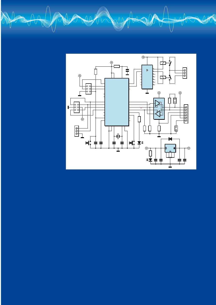
43
elektor 10-2012
E-LABS INSIDE
By Jens Nickel
(Elektor Germany Editor)
Good news for all automation
enthusiasts in general and Elek-
torBus friends in particular: more
bus hardware is in the pipeline,
including a larger Xmega board
with display and web server
module that you can use as a
control centre. The C firmware
library is on the way. More at
www.elektor-projects.com
!
Meanwhile, here’s a small E-Labs
Inside instalment, hopefully with
yet more educational value.
When we designed our RS485
relay Board [1] an extra access
point was provided to the RS485
driver’s signal ground (SIG_GND
= signal ground). The idea was to
pass on the RS485-driver ground
via an additional line run from
node to node, in parallel with
the ElektorBus ground for the
supply of each node (GND). This
was explained in the article:
“When loads are switched it is pos-
sible that there will be local inter-
ference generated on the bus ground; and if the ground poten-
tials at the drivers differ too widely this can result in spurious bits
being detected on the bus. One solution might be to connect signal
ground directly to bus ground at only one point on the bus, while in
the other bus nodes the two signals are linked via (for example) a
100 Ω resistor. … We have not yet tested this possibility…”
We received an email on this subject from Elektor reader
Andreas Schoenberg, who has been professionally engaged
with RS485 bus systems (among others) for about 25 years.
Our desire to have a “reference ground” that’s always at the
same level for all the bus drivers, appeared reasonable. However
with the LT1785 the common-mode voltage at A/B is allowed
to be in the range of –7 to +12 V (w.r.t. ground). Even when the
ground potentials of two bus nodes differ by 7 V, all bus levels
would still be interpreted correctly. Andreas Schoenberg con-
tinued, “Statically this cannot occur in the circuit. If 7 V appears
to drop on the GND line to some high-current bus node, then
an equal amount applies to the supply line, meaning a total of
14 V would be lost.” Surely that’s not possible, because the bus
supply voltage is only 12 V. He continued: “Dynamically, it cer-
tainly looks different — if a relay is energized in a module, this
can cause a short voltage dip. If so, this should be counteracted
with local capacitances at the supply pins of IC3. Provided suffi-
cient local buffering is available, I believe that ground shift prob-
lems cannot occur in your system or in the transceivers used, to
the extent of disrupting the communication.”
However, if you actually have a bus node that draws so
much power and/or is connected using long, thin wires,
that GND is at 3 V above SIG_GND due to a voltage drop,
other problems can be expected. The LT1785 at its V
CC
pin invariably ‘sees’ a voltage that’s 5 V above the local
GND potential — hence in this case it is powered at 8 V.
However the DE pin is pulled to GND via R3, and DE cannot be
pulled lower by the CPU because that too is referred to this
ground potential only. For the transceiver however, that’s still 3
V above its own ground connection (SIG_GND), i.e. always High.
The Driver Enable pin is then out of control by the software!
So much for theory. It would be interesting now to know how
you got along with the wiring of the ElektorBus hardware and
if you ran in to any problems. Here at Elektor we already estab-
lished that the communication is very robust, even with long,
el-cheapo cables and four lines [2]. Which cables did you use?
Tell us on editor@elektor.com
(120501)
[1] www.elektor.com/110727
[2] www.elektor.com/120198
Shifting
RS485 Grounds
X1
16MHz
C1
22p
C2
22p
C6
4u7
PC5/ADC5/SCL
PC4/ADC4/SDA
ATMEGA88A
PC6/RESET
PB3 MOSI
PB2/OC1B
PD7/AIN1
PD6/AIN0
PD2/INT0
PD3/INT1
PC3/ADC3
PC2/ADC2
PC1/ADC1
PC0/ADC0
PB4 MISO
PB1/OC1A
PB0/ICP1
PD1/TXD
PD0/RXD
PB5 SCK
PD4/T0
PD5/T1
XTAL1 XTAL2
IC1
ADC7
AVCC
ADC6
AREF
-AU
PB7
PB6
GND
VCC VCC
GND
GND
22
18
11
10
32
31
30
19
20
29
28
27
26
25
24
23
17
16
15
14
13
12
21
3
2
9
1
8
7
6 4
5
R8
10R
V
CC
C7
4u7
K2
1
2
3
4
5
6
C4
100n
R1
10k
S1
RESET
TEST
TEST
V
CC
ISP
MOSI
MISO
SCK
RESET
K1
1
2
3
4
5
6
V
CC
K5
3
1
2
S2
R7
1k5
LED2
DS2003
IC3
GND
DS
10
11
12
13
14
15
16
I1
I2
I3
I4
I5
I6
I7
O1
O2
O3
O4
O5
O6
O7
9
1
2
3
6
7
4
5
8
+12V
R2
10k
R3
10k
V
CC
LT1785
IC4
VCC
GND
5
8
7
6
4
1
3
2
D
R
K4
3
1
2
RE1
5
1
2
3
G5Q
RE2
5
1
2
3
G5Q
K3
1
3
2
4
6
5
R4
0R
+12V
JP1
1
2
R5
120R
JP2
1
2
110727 - 11
B
A
SIG_GND
GND
+12V
SHIELD
PHASE
S1
S2
B
A
SIG_GND
SHIELD
PC1
PC0
GND
PC1
PC0
RO
DI
DE
RE
AP78L05SG
IC2
8
1
2 3 6 7
D1
S1M
-13
R6
4k7
LED1
C5
100n
C9
4u7
C3
100n
C8
4u7
+12V
V
CC
2 29
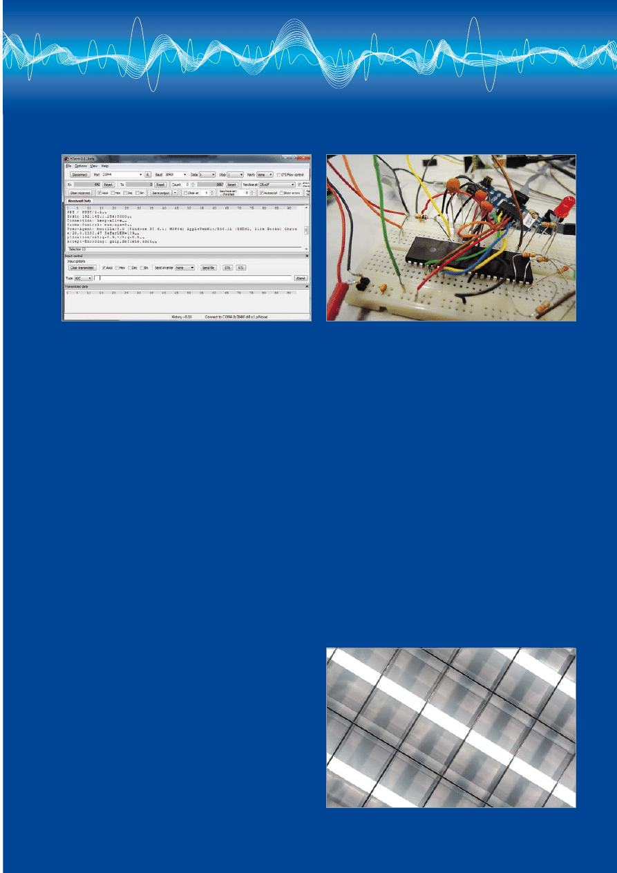
E-LABs INSIDE
45
elektor 10-2012
batten held out through a window so the antenna was well
outside the castle walls, there was still zero signal.
Suspecting the WiFi routers, PCs, laptops, fluorescent lighting,
switching wall warts and DECT telephones could be interfering
with the signal, Ton brought an old portable AM radio with long
wave band reception from home and started walking around in
the building, trying to receive the old faithful BBC4, the purpose
of this being to find the most ‘silent’ place in the castle. This
radio station transmits on long wave at 198 kHz. But nowhere
in the castle did he find a sign of the signal. It was all dirt and
noise — e-smog (Hey, didn’t we have a handily e-smog tester
shortly? Yes, we had. It’s the TAPIR. Go check it out [2]!). Only
after taking the radio more than 5 m (15 ft) outside of the castle
walls, a weak signal of the station could be heard.
When entering the building again — with the radio switched
on — Ton noticed quite some interference signals when he held
it next to the fluorescent lighting. Turns out they generate
quite some noise exactly in the 198 kHz range. So one (very)
early Monday morning, when there were very few staff present
and all the lights were still off, he tested again. But still there
was far too much noise coming from PCs, WiFi-routers, DECT
telephones, printers and other electronics that never goes
silent.
By Thijs Beckers (Elektor Editorial & Labs)
As an electronics engineer you often get to deal with electronic
as well as electrical components. Some are new and just hit the
market, others are old and have been here for ages.
Like with so many things, you probably have your own preferred
voltage regulator, Schottky diode, microcontroller, capacitor
type or even vacuum tube. But with vast numbers of Elektor
readers out there, there are bound to be differences. So here’s
a call to explain to us why this Gunn Diode you always refer to
So much for testing sensitive equipment inside the castle. A
proper worst case scenario test though; when a circuit passes
testing inside our labs, it sure is interference-proof...
Fellow lab worker Luc Lemmens experienced the same problems
with a design soon to be released. He decided to take his
testing matters elsewhere: home. As soon as he powered up
his prototype (also with a DCF77 receiver) everything came to
life and functioned as it should — right out of the box!
Ton ended up sending the prototype to an esteemed external
author for testing. And it worked instantly when he tested it. So
the lesson to be learned is: Do you want to test a prototype with
radio receiving capabilities? Don’t be too disappointed when it
doesn’t work when testing it in your lab environment. Chances
are your circuit works a treat, but e-smog from your electrical
devices is interfering with the reception of the signal.
(120504)
Internet Links
[1] www.elektor.com/100180
[2] www.elektor.com/120354
is your favourite. Tell us your experiences with that BRY39 and
elaborate on your favourite IC. Does the LM729 hold any secrets
for you? And why do you still use that 6502 for almost every job?
We look forward to a flood of emails in our inbox (myfa-
voritepart@elektor.com) and hope to be surprised by strik-
ing stories and notable narrations on your preferred electronic
component.
(120503)
Your
all-time favourite
component
2 29
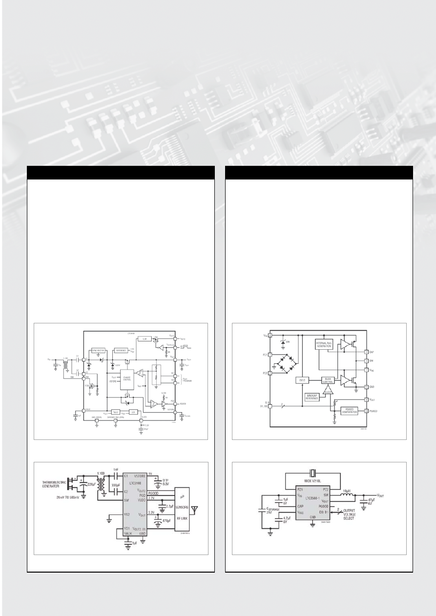
46
10-2012 elektor
Component tIpS
Energy Harvesting with the LTC3108 & LTC3588-1
By Raymond Vermeulen (Elektor Labs)
Imagine you have a sensor, which only has to report its results very infrequently and is located far away. A direct power supply is not practical be-
cause of the distance, a battery does not last forever and will eventually have to be replaced. Now what? Energy harvesting! Modern sensors can
be very frugal and just like small microcontrollers they often have a power-saving mode of operation. If the average energy requirement in this
power-saving mode is very small, then it would be possible to charge a capacitor during this long interval. This capacitor can then power the sen-
sor for a brief moment, after which it returns to a sleep state. During this sleep state the capacitor is charged once again. Below I describe two ICs
capable of deriving energy from various ambient sources. The LTC3108 is specifically intended to operate in combination with a Peltier element.
The LTC3588-1 is more suited for piezo elements. A circuit idea could be to power the ams lightning detector from last month, together with a mi-
crocontroller and RF module, using energy harvesting.
LTC3108
The LTC3108 can obtain energy from voltage sources that supply
very small voltages, starting from about 20 mV(!). This enables
the use of a small Peltier element with only a very small tempera-
ture differential. The manufacturer’s datasheet lists a number of
other potential sources. The operation is the same as that of a
boost/step-up converter with an adjustable output voltage.
An LDO with an output of 2.2 V is also present. There is an ad-
ditional Vout output that can be switched on and off and can
be used, for example, to power a small circuit that needs to be
turned on only very briefly and does not have to be placed in
some kind of power-down mode. An alternative to this chip is pos-
sibly the bq25504.
LTC3108 Datasheet
http://cds.linear.com/docs/Datasheet/3108fb.pdf
LTC3588-1
The LTC3588-a can obtain energy from a piezo element, but also,
for example, from two metal plates positioned close to a fluores-
cent light tube. The datasheet offers additional options. A piezo
element can generate a relatively high voltage, this is internally
limited by the IC to 20 V. This voltage is then reduced to an ad-
justable voltage by a buck/step-down converter.
The prescribed piezo-element in the datasheet is very expensive,
but perhaps the IC will also work in combination with a piezo
buzzer? If so, is it possible to obtain sufficient energy? This is an
invitation for some experimenting!
LTC3588-1 Datasheet
http://cds.linear.com/docs/Datasheet/35881fa.pdf
Figure 1. LTC3108 block diagram.
Figure 3. LTC3588-1 block diagram.
Figure 2. Application example using a Peltier element.
Figure 4. Application example using a piezo element.
2 29

2 29
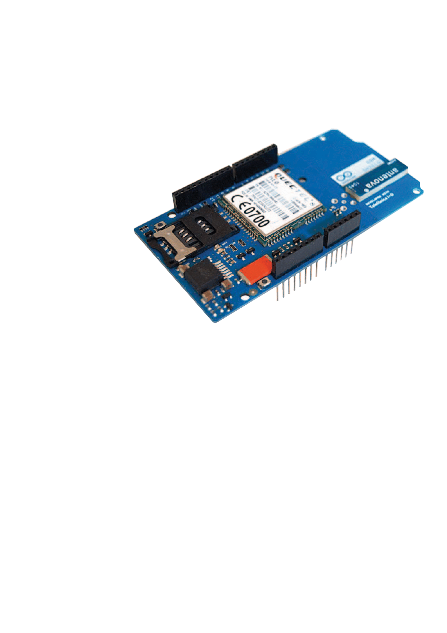
48
10-2012 elektor
Microprocessors
Arduino on Course (2)
part 2: read (awfully) remote sensors
using GsM / Gprs
By David Cuartielles (Spain)
Shopping list
In terms of hardware, here’s what you need to be able to replicate
the experiment discussed in this instalment:
•
Arduino Uno board;
•
Arduino GSM shield (made in collaboration with Telefonica I+D);
•
a SIM card for the GSM/GPRS network;
•
a cellphone (‘mobile’) with its own SIM card;
•
TinkerKit shield;
•
TinkerKit LED module (x3);
•
TinkerKit Slider module.
The last three items in the list can be substituted by a breadboard
and a combination of various components. However, to keep the
focus on the operation of the GSM library for Arduino, I have opted
to use pre-assembled parts.
Now, before you read on, I strongly recommend you download all
the code used this month. Due to the length of the example pro-
grams, only excerpts are printed here.
Introduction to M2M and IoT
Putting it in easy terms, IoT is a computing paradigm that is being
explored lately by many research laboratories and universities
around the world. It tries to bring to life the idea that everything can
be connected to the Internet: your microwave and your car, passing
by your door lock and your bike at the gym. All those objects should
be able of talking to each other in some way and exchange data to
offer people better ways to handle different situations.
Ericsson, the Swedish communication giant, presented a memo
[1] last year where
they envisioned that
by 2020 there would be 50
billion connected devices. That
would mean that most of our home
appliances are connected to the Internet:
fridges and microwaves, alarm clocks and TVs,
the elevator and the stove. But also all the other devices that
surround us like cars, streetlights, or shopping carts (the push-
able type, not the icon or applet).
M2M (machine-to-machine) is concerned with the connectivity
between devices using wireless, wired or hybrid communication.
In a sense, M2M makes IoT (Internet-of-things) possible as it offers
the infrastructure for devices to gather data and transmit it through
a network to a remote location. For some people M2M is a synonym
of telemetry in whatever form, but in recent years the concept has
mutated to refer mostly to wireless communication and to be more
specific it is mostly referring to the use of cellular (mobile) commu-
nication for remotely controlling devices.
For the sake of simplicity, when talking about the IoT I mean the
connection of devices to the Internet, while M2M will be a way to
make this possible through the cellular telephony network. You
will find many articles and videos on the Internet that follow the
same approach, the reason being that the most extended net-
work right now is the one called GSM (global system for mobile
communications).
I assume that you are reading this article because you plan on mak-
ing a connected device. Imagine that you create an object that’s
going to connect to the Internet and send data back to you from
anywhere in the world — what, do you think, is the best way to do
so? The answer is obvious: cellular telephony. GSM is a great alter-
native as it allows you contact your device almost anywhere in the
world knowing that it will work, basically like at home.
The Arduino - GSM/GPRS Shield
From Arduino we want to simplify as much as possible the way
you build prototypes and learn about technology. Therefore we
have spent quite some time thinking about how to help you get-
This month we’ll explore the
possibilities offered by GSM
and GPRS communication for
your projects. We will
link concepts like the
Internet of Things (IoT)
or the Machine To Machine
(M2M) business in order to
understand what you can achieve
all by yourself in a short time.

49
elektor 10-2012
Arduino on course
ting hooked to this trend of IoT in many ways. One of them is
through M2M and for that we teamed up with Telefonica’s Physi-
cal Internet Laboratory.
We have been collaborating in making an official Arduino shield that
easily handles GSM/GPRS (also known as 1G and 2G) communication.
We also wrote a library that simplifies the process of texting (SMS
transmission), setting up calls or publishing some data on a website.
The design is open source and the software can easily be ported
to support other shields (with potentially other series of AT-Com-
mands; more about this later). Finally, the shield comes with a SIM
card, courtesy of Telefonica, that will offer you the possibility to
hook up to send/receive text (SMS), set/get voice calls, and con-
nect to the Internet through the GPRS network.
Note: This shield is not locked to the accompanying SIM; you could
use any other GSM/GPRS SIM card available in your country. The
SIM is optimised for data communication; if you wanted to make
something controlled over Text (SMS), you should consider a SIM
card operating on your preferred network. If you were about to use
the card coming with the board, you should follow the online acti-
vation instructions that come with it.
Controlling a modem - AT commands
Modems are the devices behind the expansion of the Internet. In
order to automate the way they would operate, a company called
Hayes [2] invented in 1981 what would later be called the AT-Com-
mand Set. The idea behind it all is for modems to change between
Command and Data operation modes. The Command mode would
allow performing operations on the modem itself like calling a cer-
tain number, changing the baud rate (the speed at which the data
would be transferred), etc.
The Hayes Command Set became a de-facto standard for the way
devices should communicate over a serial port. That standard is still
operating inside many devices. When in Command mode, devices
start the communication sending the string “AT” which stands for
“attention”. That would be followed by other strings that would
translate in different operations to be performed at the other side.
On the other hand, when in Data mode, the data will just be proxied
to/from the Internet through the modem.
The GSM/GPRS shield has a radio modem manufactured by Quec-
tel [3] that can be operated using a series of AT commands. Most of
those commands are specific to the modem on the board, but the
library that controls the shield has been written in a way that makes
very easy to port it for other modems made by any manufacturer.
Also, the library hides all the complexity behind this mode of opera-
tion. Therefore, we are not going to refer to them in the rest of the
article. However, if you happened to use the GSM library in debug
mode, you would be prompted with many of those commands.
Installing the GSM Library for Arduino
At the time of writing this article the Arduino IDE had reached revi-
sion 1.0.1 and did not include the GSM library we’re about to dis-
cuss. Thus, when checking the menu ‘Sketch / Import Library’ if you
don’t see the library named ‘GSM3’ in the list, you will have to down-
load it from the official Arduino website hosting this project [4] and
install it as explained under the ‘Library’ link. Essentially, adding a
new library to the IDE is done by creating a folder called ‘libraries’
inside your sketchbook and uncompressing the file you got from the
website [4] directly there. After that, you should restart the Arduino
IDE and the library will then show up in the above mentioned menu.
With the library you will be installing not only the code to execute
different commands on the modem, but also a series of examples
that will allow you to:
•
test whether the modem is working properly;
•
text, i.e. send/receive SMS;
•
place/get phonecalls (voice);
•
open a TCP/IP connection and exchange data over the Internet,
using GPRS;
•
post/collect sensor information to/from Cosm (an online data
service);
•
collect and show twitter messages.
The way to access the examples is simple: just use the menu to navi-
gate through “File / Examples / GSM3”.
Checking your status
Likely, the first thing you want to do is checking whether your board
is working properly and whether your SIM card can be used by the
shield for you to experiment with. To do so, open the example under
// libraries
#include <GSM3ShieldV1ModemVerification.h>
// modem verification object
GSM3ShieldV1ModemVerification modemTest;
// IMEI variable
String IMEI = “”;
// serial monitor result messages
String oktext = “OK”;
String errortext = “ERROR”;
void setup()
{
// initialize serial communications
Serial.begin(9600);
// start modem test (reset and check response)
Serial.print(“Starting modem test...”);
modemTest.begin();
Serial.println(oktext);
}
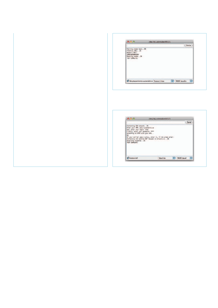
50
10-2012 elektor
Microprocessors
the menu: “File / Examples / GSM3 / Tools / TestModem”.
This code example allows you to check whether Arduino can detect
your radio modem. It also opens a connection to the radio modem
on your GSM shield and attempts to read the IMEI (International
Mobile Equipment Identity) from it — that’s a unique number for
every device capable of connecting to the GSM/GPRS/3G/4G net-
work. For example, your cell phone identifies itself via the IMEI.
Every device on the GSM network has a unique ID. If everything goes
fine, after uploading the example on your Arduino Uno, and opening
the Serial Port Monitor, you should see something like in Figure 1.
If your modem was working correctly, the next thing is to check
whether you can connect to the GPRS network. To do so, we will
open the example: File / Examples / GSM3 / Tools / TestGPRS. I will not
show the code here, as it is very similar to the previous one. This
example is used for testing that your SIM card allows connecting to
the GPRS network (the one provided with the shield does), but also
to test your settings.
Note: this shield is using GSM/GPRS technology and not 3G. 3G and
GSM SIM cards look the same, but remember that some of the mod-
ern operators do not offer 2G (the way we call GPRS) services.
Connecting to the GPRS network calls for a tad more configuring
than just texting (sending an SMS) or placing a call. There are four
parameters that need to be configured:
•
APN: acronym for Access Point Name or the name of the
domain the shield will connect through to reach the Internet.
It is specific for the operator providing you with connectivity
through the shield;
•
login: some operators require a login;
•
password: some operators require a password;
•
proxy: this is the address to a server that will channel all your
communication inside the operator’s network. Most likely it
won’t be used.
The way this example works is by asking you for the information the
shield needs to connect to the network.
Tip: remember activating the option ‘Newline’ in the dropdown
menu at the bottom of your Serial Port monitor. In this way, when
clicking on ‘Send’ on the monitor, the system will add an end-of-line
(EOL) character that is needed for the modem to know the informa-
tion package came to an end.
I everything goes fine, you will see a window like in Figure 2. Those
messages mean that your shield can connect to the Internet using
your SIM. Please note that even if you couldn’t connect to the Inter-
net, it may still be possible for you to text-out, get text (send/receive
SMS) and set up calls.
Texting (sending an SMS)
Texting or receiving text (sending or receiving SMS) with the GSM
void loop()
{
// get modem IMEI
Serial.print(“Checking IMEI...”);
IMEI = modemTest.getIMEI();
// check IMEI responsed
if(IMEI != NULL)
{
Serial.println(oktext);
// show IMEI in serial monitor
Serial.println(“Modem’s IMEI: “ + IMEI);
// reset modem for check booting
Serial.print(“Reseting modem...”);
modemTest.begin();
// get and check IMEI one more time
if(modemTest.getIMEI() != NULL)
{
Serial.println(oktext);
Serial.println(“TEST COMPLETE!”);
}
else
{
Serial.println(errortext);
}
}
else
{
Serial.println(errortext);
}
while(true);
}
Figure 1. Positive answer from the TestModem example using the
Serial Monitor.
Figure 2. Configure your GPRS connection using the Serial Monitor.
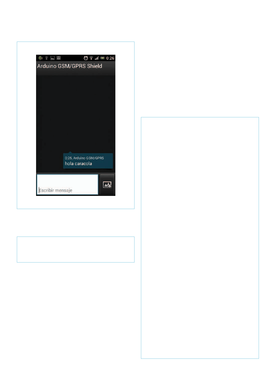
51
elektor 10-2012
shield couldn’t be any easier. The following lines of code could be
part of a program sending a string to a certain number.
Note that I am using a fictitious cell phone number! And the result
on the screen of my phone would be like shown in Figure 3.
The library comes with examples covering both sending and receiv-
ing. For example, the code at File / Examples / GSM3 / Tools / SendSMS
will be sending an SMS (texting out) from the board to a phone via
interaction through the Serial Port Monitor. It will first ask you for
the phone number to text to (SMS) and then for the string to send.
Try it out!
Remotely controlling a device via Text (SMS)
Controlling a device remotely implies receiving messages, parsing
the data, and operating actuators depending on the different com-
mands. In this case we are going to build a quick prototype includ-
ing three LEDs: one red, one green and one blue. You can imag-
ine that instead of using LEDs we could be attaching relays, and we
could be controlling any kind of device on distance. The program
is going to read the first character sent in the SMS and turn on the
corresponding light: R for red, G for Green and B for blue. This pro-
gram is, as you can see, very simple. It doesn’t execute huge parsing
operations; it simply reads the first character in the text message
(SMS) and decides what to do. After that, the text message (SMS)
will be erased from the memory using the command sms.flush().
// send the message
sms.beginSMS(“0755442200”);
sms.print(“hola caracola”);
sms.endSMS();
// If there are any SMSs available()
if (sms.available())
{
Serial.println(“Message received from:”);
// Get remote number
sms.remoteNumber(remoteNumber, 20);
Serial.println(remoteNumber);
// This is just an example of message disposal
// Messages starting with # should be discarded
if(sms.peek()==’#’)
{
Serial.println(“Discarded SMS”);
sms.flush();
}
// Read message bytes and print them
int count = 0;
while(c=sms.read()) {
if(!count) {
digitalWrite(pinR, LOW);
digitalWrite(pinG, LOW);
digitalWrite(pinB, LOW);
switch(c) {
case ‘R’:
digitalWrite(pinR, HIGH);
break;
case ‘G’:
digitalWrite(pinG, HIGH);
break;
case ‘B’:
digitalWrite(pinB, HIGH);
break;
}
}
count++;
}
Serial.println(“\nEND OF MESSAGE”);
// delete message from modem memory
sms.flush();
Serial.println(“MESSAGE DELETED”);
}
Figure 3. Screenshot of my phone after I was texted.
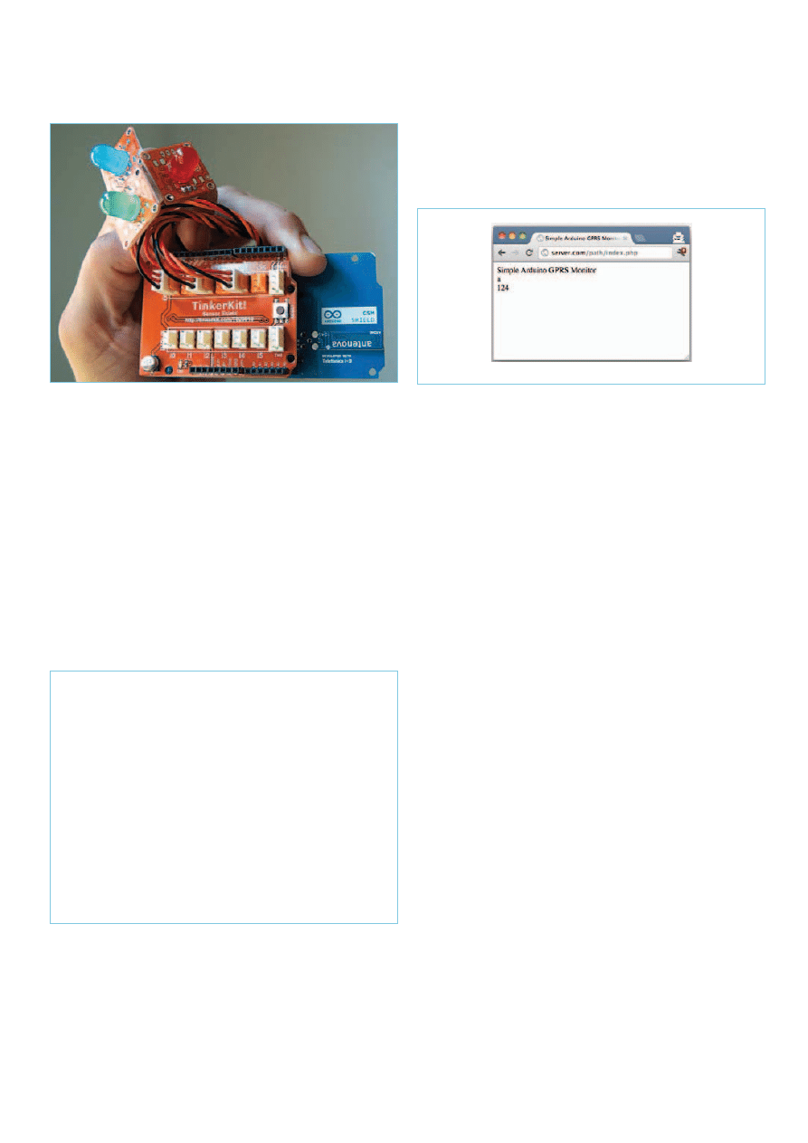
52
10-2012 elektor
Microprocessors
The following is a part of the example DecodeSMS you can find at
the download link [5] for this article.
The actual circuit boards are shown in Figure 4.
Device working over GPRS
Let’s now see how to use an analogue sensor (a slider in this case) and
send data from it to a website. On the server side I am using Apache
and a very simple PHP script that will be taking the data sent by the
board and will update a part of the script containing plain HTML. This
is what I like to call a simple ‘online memory cell’. It is a PHP script
that can take the data and display it. It will be possible to access that
same page using a browser to see the data changing over time. You
will need to use the same APN/login/pass combination you used in
the previous GPRS example for this code to work properly. Here’s how
to send an analogue value to a server every 10 seconds:
You need to have a server to run the php code that will be reading
from your Arduino board. The server needs to be publicly accessible
as you want your Arduino board to post information to it and to read
that data using a browser, a phone or any other web-enabled device.
Important: keep in mind that this code is just a proof of concept, it is
not safe in any way and you should probably disable the PHP script
once you are done trying out the example.
The only thing left to do is uncompress the code of the PHP mem-
ory cell in the given file [5] at the root folder, to your http server.
Make sure the file has read-write-execute permissions to allow it to
rewrite itself. You can then type the URL to your server (for example:
http://server.com/path/index.php) in a browser to see the informa-
tion update every 10 seconds. Like in Figure 5.
Closing words
I hope you found this brief introduction to the use of GSM/GPRS
technology in your projects both educational and fun. I want to
highlight how relevant it is that we, as makers, can benefit from
the existence of an omnipresent wireless network. If you don’t need
very data-hungry devices, you could start controlling lots of things
over the cellphone network. As long as there is a way to power up
your board, you can gather and process data from almost anywhere.
(120506)
Internet Links
[1] Ericsson’s memo on 50 billion connected devices:
www.ericsson.com/res/docs/whitepapers/wp-50-billions.pdf
[2] on the AT-Command set:
http://en.wikipedia.org/wiki/Hayes_command_set
[3] Quectel AT-Command description:
http://datasphere.eu/en?t=/documentManager/sfdoc.file.
supply&fileID=1285079825955
[4] Arduino website hosting information about the GSM shield:
http://labs.arduino.cc/GPRS/Index
[5] Compressed file with all the examples and images:
www.elektor.com/120506
Acknowledgements
My sincere thanks are due to the whole Physical Internet Laboratory
team at Telefonica Research and Development, for their support in
making this new Arduino shield possible. Special thanks go out to F. J.
Zorzano for being there debugging code until late many nights.
Figure 4. All in hand: Arduino Uno + GSM/GPRS shield +
TinkerKit shield + TinkerKit LED.
Figure 5. Information being displayed on a browser as sent from
the GSM shield.
void loop()
{
client.connect(server, 80);
Serial.println(“sending data...”);
client.print(“GET “);
client.print(path);
client.print(query);
client.print(analogRead(A0)); // take the value
// on A0 and send it
client.println(“ HTTP/1.1”);
client.print(“HOST: “);
client.println(server);
client.println();
client.stop();
delay(10000);
}

53
elektor 10-2012
· Coast Electronics · CS Technology · Easysync · Elnec · FTDI Chip · Robot Electronics ·
Surf to www.elektor.com
365 days per year preferred suppliers online with up to date and relevant information.
To become a preferred supplier contact Johan Dijk by j.dijk@elektor.com
FIRST TECHNOLOGY TRANSFER
LTD.
http://www.ftt.co.uk
• Training and Consulting
for IT, Embedded and
Real Time Systems
• Assembler, C, C++ (all levels)
• 8, 16 and 32 bit microcontrollers
• Microchip, ARM, Renesas, TI, Freescale
• CMX, uCOSII, FreeRTOS, Linux operating
systems
• Ethernet, CAN, USB, TCP/IP, Zigbee, Bluetooth
programming
ROBOTIQ
http://www.robotiq.co.uk
Build your own Robot!
Fun for the whole family!
Now, available in time for X-mas
• Arduino Starter Kits *NEW!!*
• Lego NXT Mindstorms
• Affordable Embedded Linux Boards
• Vex Robotics (kits and components)
• POB Robots (kits and components)
email: sales@robotiq.co.uk Tel: 020 8669 0769
SCOPES
and more
Great Value in
TEST & MEASUREMENT
www.hameg.com
www.elektor.com
www.elektor.com
www.elektor.com
www.elektor.com
www.elektor.com
www.elektor.com
The HRLV - MaxSonar Sensors
$PD]LQJ 2QH0LOOLPHWHU 5HVROXWLRQ
6LPXOWDQHRXV 0XOWLSOH 6HQVRU 2SHUDWLRQ
6XSHULRU 1RLVH 5HMHFWLRQ
7DUJHW 6L]H &RPSHQVDWLRQ IRU $FFXUDF\
7HPSHUDWXUH &RPSHQVDWLRQ
2XWSXWV QRZ LQFOXGH 77/ 6HULDO
$
34.
95 (MSRP)
www.MaxBotix.com
TYDER
http://www.tyder.com
• ONEoverT Digital Filter Design Software (Full
version for only £30)
• Design FIRs, IIRs, NCOs, FFTs for DSPs and
FPGAs
• VHDL Code Generators
• Makes DSP design
simple
• Download demos from
website
T ON ELECTRONICS AND
ON TECHNOLOGY
S AND INTERESTING OFFERS
WN MAILBOX EACH &RIDAY
Take out a FREE
membership to
Elektor Weekly
2EGISTER TODAY AT WWWELEKTORCOMNEWSLETTER
JOIN THE WORLD’S LEADING PLATFORM FOR ELECTRONICS ENGINEER
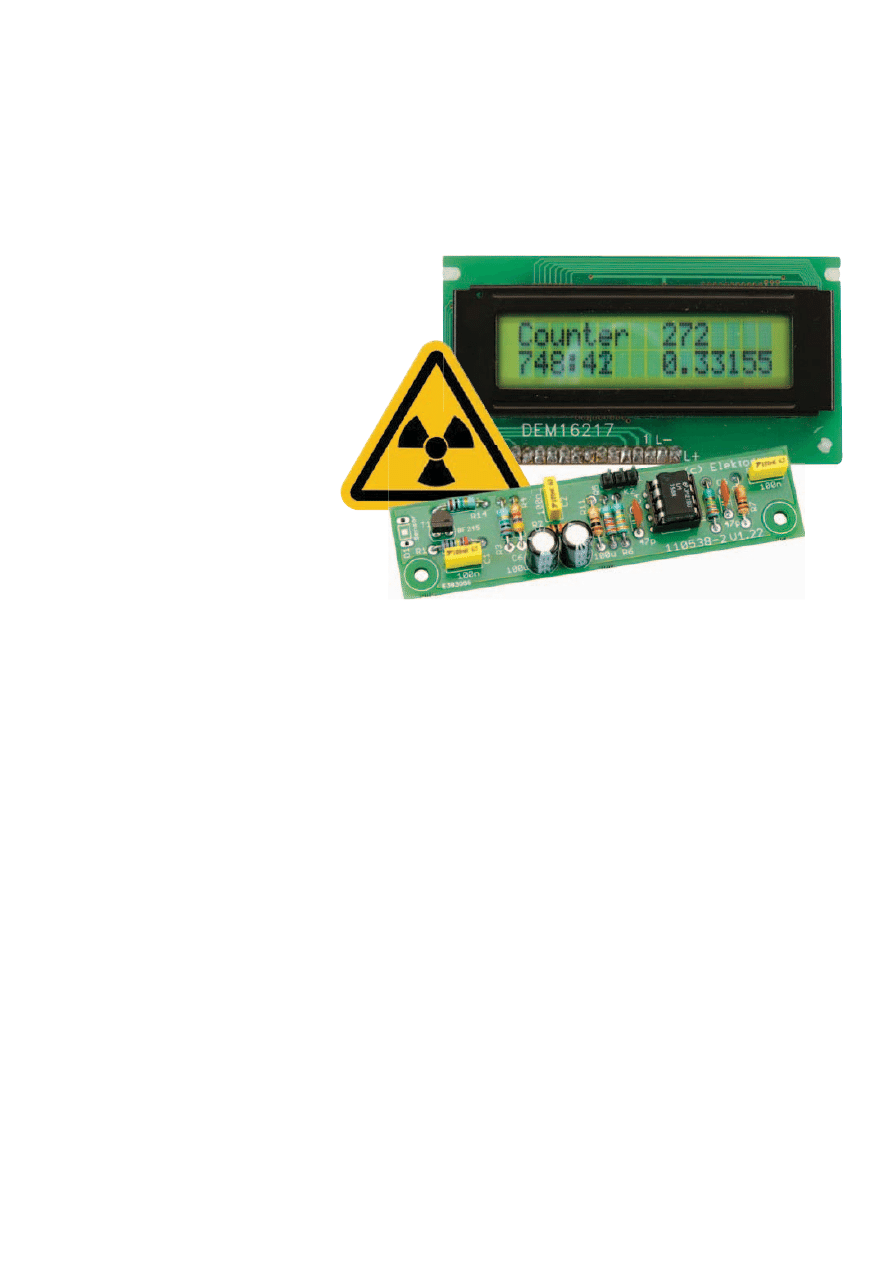
54
10-2012 elektor
TesT & MeasureMenT
Radiation Meter Reloaded
simple modifications open up
new possibilities
The ‘Improved Radiation Meter’ was pub-
lished in Elektor in November 2011 [3]. The
device is available as a kit of parts [2], the
ATmega88 microcontroller being equipped
with a bootloader that makes it easy to pro-
gram your own code into it. Some applica-
tions will require just a small change to the
code in the basic program, and below we
will look at a couple of examples of this.
Other applications will require firing up the
soldering iron to make more permanent
changes: we will look at some of the pos-
sible hardware modifications first.
Calibration
The following question often crops up in our
readers’ forum: can the radiation meter be
calibrated in standard units such as micro-
sievert per hour (µSv/h)? This turns out not
to be so easy, as several variables enter into
the equation. The most significant of these
is the screening used.
Experience with the radiation meter shows
that it is not easy to screen the sensor com-
pletely from light without simultaneously
also blocking the radiation we are inter-
ested in to a significant extent. Two options
are open to us: we could put the sensor and
the sample being studied together in a
metal can connected to ground, or we could
wrap the whole sensor board in aluminium
foil, which again must be grounded. Some
readers have experienced problems with
the latter approach arising from a microph-
ony effect: the sensor forms a kind of con-
denser microphone with the foil shield. The
effect can be mitigated by gluing the foil
directly to the sensor. Self-adhesive copper
foil, 0.035 mm thick, has also been found to
work well in practice: it also has the advan-
tage that it is easier to solder the ground
connection to it.
We tried an experiment using a BPW34
sensor with a copper foil shield. The radi-
ation source was a thorium gas lantern
mantle in its paper envelope. Because
this source has a large area the radiation
level at close quarters is approximately
uniform, which means that the readings
obtained are largely independent of the
distance between source and sensor. The
Elektor radiation meter gave approximately
40 pulses per minute at a distance of 1 cm.
For comparison we used a professional Gei-
ger counter with a tube sensitive to beta
and gamma radiation, again at a distance
of 1 cm. This gave a reading of 800 pulses
per minute, corresponding to 20 µSv/h.
This gives us our first unofficial calibration
result:
1 pulse/min = 0.5 µSv/h
In principle the unit is capable of measuring
the level of background radiation if readings
are taken over a sufficiently long period.
Over very long periods it is possible to see a
clear change in readings with variations in
solar activity. The somewhat longer meas-
urement period required than with a Geiger
counter does of course make some applica-
tions less practical: for example, if you try
to measure the radiation from a salad you
may well be lucky enough to discover that
it is safe to eat, but by the time you know
that your rocket will probably have wilted!
The device is better suited to investigat-
ing small, weakly radioactive, samples
than to analysing the background radia-
tion. Here the small sensor sizes gives the
device an advantage over the Geiger coun-
ter, as it makes it easier to discriminate
between radiation from the sample and the
background.
AC coupling
There is a further technique we can use to
reduce the sensitivity to ambient light: we
By Burkhard Kainka (Germany)
The radiation meter published in the
November 2011 edition of Elektor is
currently being used by many readers,
mainly in making long-term
measurements and in investigating
weakly radioactive samples. There
are several ways in which we can
modify and improve the design, and we
look here at a few examples.
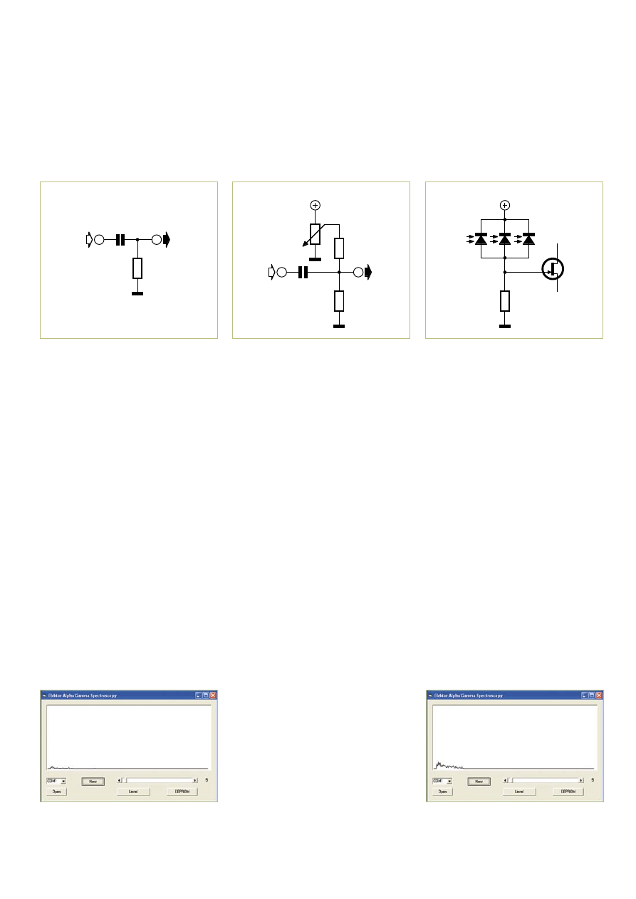
55
elektor 10-2012
radiaTion MeTer reloaded
can add AC coupling between the sensor
board and the counter. A 100 nF capacitor
and a 10 kΩ resistor will do the job (Fig-
ure 1). The circuit operates as a high-pass
filter with a corner frequency of 160 Hz. It
now does much less harm if light should fall
on the sensor and shift its operating point.
Flickering from artificial incandescent light-
ing at a frequency of 100 Hz is also some-
what attenuated. However, it does little to
reduce the effect of fluorescent lights as
these produce sharper flashes of light. Nev-
ertheless, the filter modification does make
the circuit more stable generally and con-
siderably less sensitive to light.
If desired, a potentiometer can be added to
the circuit to allow adjustment of the coun-
ter trigger threshold (Figure 2). Although
this facility was already available in the PC
software accompanying the design, some
readers use the unit to make measure-
ments ‘in the field’ without a PC attached:
if you are taking readings while scrambling
around in a quarry, you will probably pre-
fer not to risk lugging an expensive laptop
about as well. The suggested circuit shifts
the average threshold by up to 50 mV.
By default the software sets the trigger
threshold to 10, which corresponds to
approximately 50 mV. At start-up the micro-
controller measures the average voltage at
its input and adds this value to the thresh-
old: any pulse with amplitude exceeding
this value will be counted. With the new
AC coupling circuit the microcontroller
will measure the average noise level on the
input, obtaining, for example, a value of 5.
The trigger threshold will then be 15. With
the addition of the potentiometer the qui-
escent level can be increased to as much
as 50 mV. At start-up the potentiometer
should be set to its lowest point. Then the
threshold can be adjusted carefully towards
the noise floor to determine the point
where sensitivity is greatest. A press of the
‘Zero’ button will then start a fresh series of
readings with the new threshold setting.
Sensors and results
In its standard configuration the device uses
a single type BPW34 PIN diode as its sen-
sor. However, it is possible to wire several
BPW34s in parallel (see Figure 3). The effect
of this is to produce meaningful readings in
a shorter time. It is possible either simply to
count the pulses or to use the more sophis-
ticated program that analyses the energy
spectrum.
Before carrying out a measurement it is
a good idea to do a calibration measure-
ment to estimate the background radia-
tion level. Figure 4 shows such a calibra-
tion measurement with three BPW34s
wired in parallel. The trigger threshold
used was 5. Forty pulses of varying ener-
gies were detected over the course of
one hour. These results can be subtracted
from the subsequent measurement to
improve accuracy when using weakly
radioactive samples.
Potassium chloride (or more accurately the
potassium-40 in it) exhibits weak beta activ-
ity. Perhaps easier to obtain is potassium
carbonate (or ‘carbonate of potash’), which
is sometimes used in baking. A sample of
this substance was placed in a small plastic
bag next to the sensor. Figure 5 shows the
results, taken over one hour. A total of 251
pulses were counted, some six times the
background level.
10k
100n
Sensor
Counter
10k
100n
Sensor
Counter
10k
1M
+5V
Figure 1. AC coupling.
Figure 2. Setting the trigger threshold.
+9V
20M
3x BPW34
Figure 3. Three BPW34s in parallel.
Figure 4. Calibration measurement using
three BPW34s in parallel.
Figure 5. Radiation from
potassium carbonate.
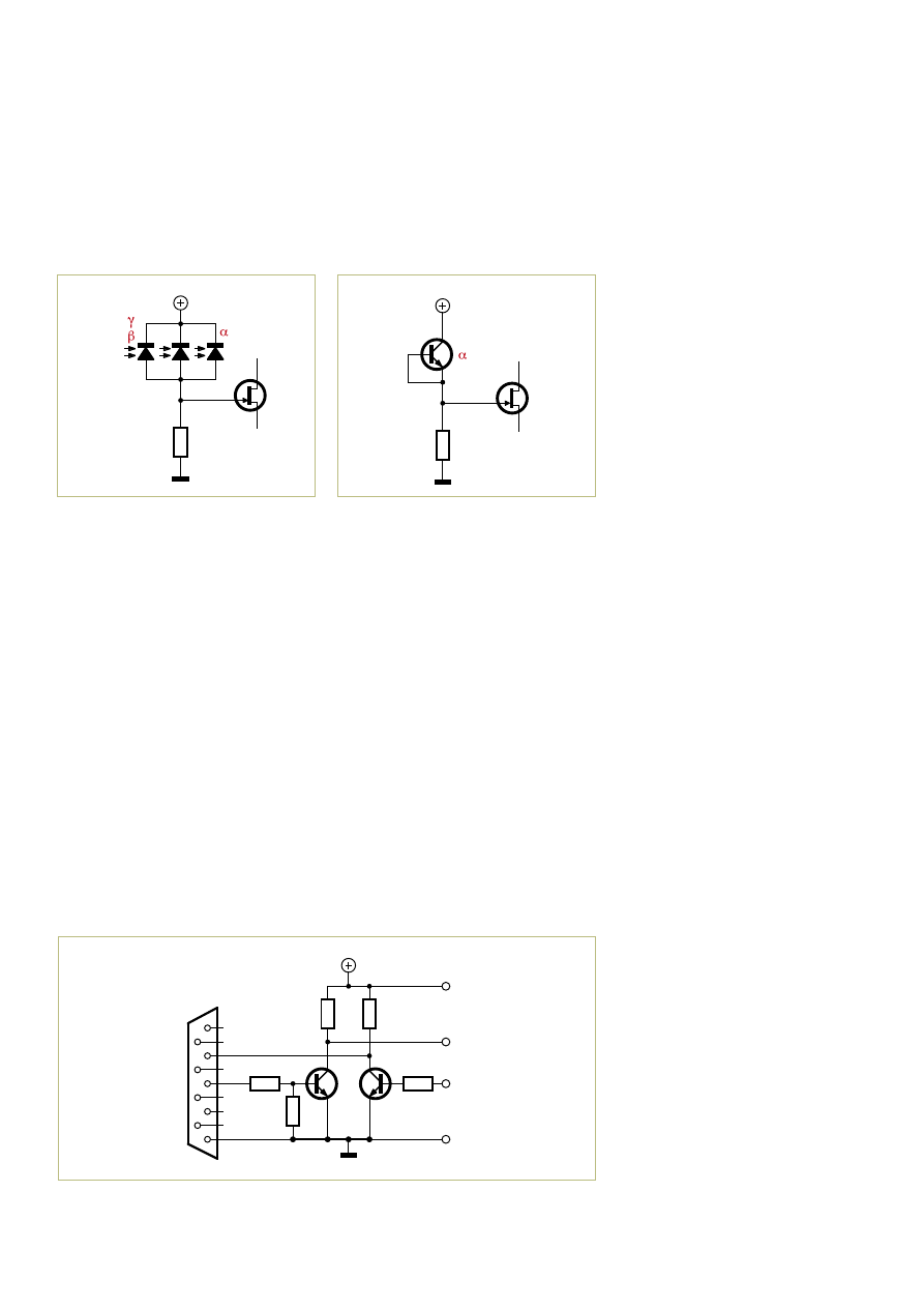
56
10-2012 elektor
TesT & MeasureMenT
Alkaline batteries do not normally leak;
however, when they do, the concentrated
potassium hydroxide in them reacts with
the CO
2
in the atmosphere to form potas-
sium carbonate. This is seen as a white resi-
due where the leak has occurred. This res-
idue should be a weak radioactive source,
and indeed this can be confirmed using the
radiation meter.
With the sensor set up for maximum sensi-
tivity, including for low-energy pulses, we
can use the radiation meter with samples
of even lower activity. This can be seen in
an experiment with charcoal ash from the
barbecue, which contains potassium car-
bonate. We measured a radiation level of
approximately 150 pulses per hour from
a sample. We can even find radioactiv-
ity in cigarette ash: in one experiment we
obtained 80 pulses per hour, double the
background level. Again, the main source
of the radiation is probably potassium,
although polonium, a product of uranium
decay, may also play a part as it is accumu-
lated in tobacco plants.
Alpha decay
Using an exposed BPX61 photodiode lets us
also detect alpha particles. In fact, we can
use both types of diode together: a BPW34
to detect beta and gamma radiation, and a
BPX61 for alpha particles (see Figure 6).
To test this combination we first measure
the weak radiation from a sample of potash
or potassium carbonate and set the trig-
ger threshold appropriately. Once this has
been done successfully, we can move on to
making the more difficult measurements,
including on various building materials
whose level of activity may be of interest.
Alpha particles are distinguished by their
higher energy: we can often find noticeable
levels of radiation in plasterboard, because
the gypsum used in its manufacture is made
by the desulphurisation of flue gases from
coal-fired power stations and, in turn, the
coal contains a small amount of uranium
and its various decay products.
The 2N3055 as an alpha particle
detector
When alpha particles hit a silicon junction
a relatively strong signal is produced. That
is true not just for photodiodes, but for any
type of diode or transistor. Under normal
circumstances alpha particles do not get as
far as the junction as they are absorbed by
the devices package or shielding. However,
we can get around this in the case of certain
power transistors in a TO-3 package: if we
remove the metal cap the silicon chip itself
is revealed, with its relatively large surface
are exposed to the elements.
This is usually the case for the famous
2N3055; for other devices there is some-
times an additional protective layer, and
so sometimes a little luck is needed to find
one that is suitable. A fairly recently-pro-
duced transistor from ST was found to work
well (see Figure 7). The chip is completely
exposed and makes an excellent alpha par-
ticle sensor. Beta and gamma radiation,
however, go completely undetected. Fig-
ure 8 shows the result with a sample of
pitchblende (uranite). When tested with
an americium-241 source from a smoke
detector more pulses were produced than
the counter could cope with.
Serial interface
The counter board includes a three-pin con-
nector which gives access to the serial port
on the microcontroller, the RXD and TXD
signals being at TTL levels. The connector is
compatible with the Elektor breakout board
(‘BOB’) [1], based on the FT232R, and so
allows connection to a PC over USB using a
virtual serial port.
A very simple extension allows the device
to be connected to a standard RS-232 inter-
+9V
20M
2x BPW34
BPX61
+9V
20M
2N3055
RS232
1
2
3
4
5
6
7
8
9
47k
100k
+5V
10k
10k
BC547B
2x
PC
100k
RXD
TXD
GND
GND
PD1,TXD
PDO, RXD
+5V
Figure 6. A combination
of different sensors.
Figure 7. Using a power transistor as an
alpha particle sensor.
Figure 9. RS-232 level shifter.
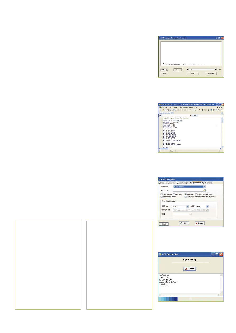
57
elektor 10-2012
radiaTion MeTer reloaded
face. Two NPN transistors do the job of shift-
ing the voltage levels and inverting the sig-
nals (see Figure 9). With this circuit you can
connect the radiation meter to a PC with an
ordinary serial port or to a USB-to-RS-232
adaptor.
The PC-based program can be installed to
provide the ability to plot energy spectra
and to adjust the trigger threshold. It also
provides the additional useful function of
uploading program updates (or even com-
pletely new programs) into the microcon-
troller over the serial port.
Program upload
Suppose we would like to make a change
to the way the counter works. The boot-
loader facility in the microcontroller makes
this easy, and it even works with the ‘Demo’
version of BASCOM (Figure 10). First open
the BASIC source code and then, after mak-
ing any changes to it, compile it.
Select the programmer to be used in BAS-
COM. In this case it is ‘MCS Bootloader’. The
COM port and baud rate (19200) also have
to be set correctly (see Figure 11).
Now start the programmer, for example by
using the small green circuit board icon. The
MCS Bootloader will now try to establish a
connection with the microcontroller.
The connection can only be established
shortly after the microcontroller is powered
up or reset. So, switch the device off and
then on again, and programming should
commence (Figure 12).
When all the code has been uploaded the
microcontroller immediately starts to exe-
cute the new program.
Software variants
In-depth BASIC programming skills are
not needed to make small changes to the
program and to upload the new code to
the microcontroller. Here are a couple of
examples.
1. Constant trigger threshold (Listing 1).
Suppose we always wanted to have the trig-
ger threshold equal to 5. All that’s required
is to add the line ‘L = 5’ at the right point
in the program. We can also get rid of the
‘Counter’ message at start-up by simply
commenting out the relevant lines by add-
ing a single quotation mark at the begin-
ning. A further change is also shown in List-
ing 1, but commented out for now so it has
no effect: the line ‘Um = 0’ sets the aver-
age level to zero, which is better suited to
use with the AC coupling circuit shown in
Figure 1.
2. Measuring the energy distribution
(Listing 2)
Our second example shows how to count
Listing 1: Changes in Counter_1
‘Print “Counter”
Locate 1 , 1
‘Lcd “Counter”
‘Waitms 500
Readeeprom L , 1
If L = 255 Then L = 5
U = 0
For N = 1 To 1000
D = Getadc(0)
U = U + D
Next N
U = U / 1000
Um = U
‘Um = 0
U0 = Um + L
N = 0
Listing 2: Changes in Counter_2
Do
D = Getadc(0)
If D > Maxi Then Maxi = D
Loop Until D < U0
Maxi = Maxi Um
If Maxi > 255 Then Maxi = 255
N = N + 1
If Maxi > 40 Then N2 = N2 + 1
If Maxi > 80 Then N3 = N3 + 1
Locate 1 , 1
Lcd N
Lcd “ “
Locate 1 , 8
Lcd N2
Locate 1 , 14
Lcd N3
Figure 8. Measurement using an old faithful
called 2N3055.
Figure 12. Programming is successful!
Figure 11. Selecting the programmer.
Figure 10. The BASCOM development
environment.
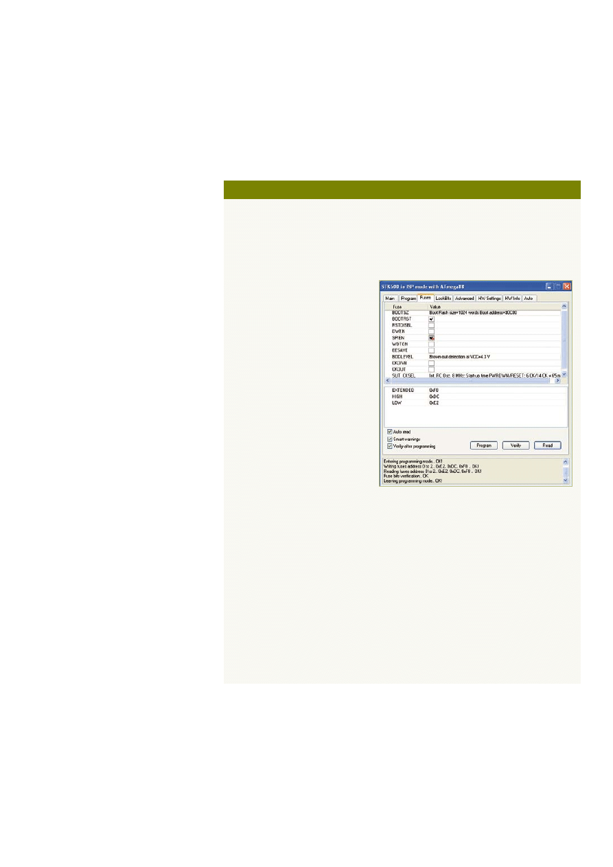
58
10-2012 elektor
TesT & MeasureMenT
pulses separately according to their
energy. We will have three counters, one
for all results (N), one for pulses with a level
exceeding 40 (N2), and one for the highest-
amplitude pulses, with a level exceeding 80
(N3). All three counts will be displayed on
the top line of the display. The values give
a broad indication of the energy distribu-
tion without the need to connect a PC to
plot a graph. The fact that we can discrimi-
nate energy levels in this way is a significant
advantage of the semiconductor sensor
over a conventional Geiger counter.
Other substances to examine
The question often arises of what sub-
stances can be used to test the operation
of the device. In the original article we sug-
gested using a sample of uranite, a lumi-
nous watch, and potassium chloride. Below
we give a few more ideas.
Uranium glass is still made. It is used in dec-
orative fluorescent glass beads.
Type WT20 tungsten inert gas (TIG) weld-
ing electrodes are made of tungsten with
the addition of a 2% thorium oxide compo-
nent. The electrodes are weak alpha, beta
and gamma sources.
Tungsten with added thorium is also used in
the directly-heated cathodes of large radio
transmitter valves, although admittedly
such devices are not exactly found on every
street corner. However, the same material is
used in the magnetron in a domestic micro-
wave oven: a salvaged magnetron cathode
makes an effective test source.
Thorium salts were used in the mantles for
gas and paraffin lamps in the past, although
modern mantles use different substances. If
you can manage to get hold of an old man-
tle, you will find it makes a particularly pow-
erful test source, including of high-energy
gamma rays.
Ionisation smoke detectors use a strong
(perhaps 33 kBq) alpha source. Such detec-
tors are common in the USA and in the UK
but much less popular in mainland Europe.
The gamma rays produced by the substance
are relatively weak, and so a BPW34 only
produces about 30 pulses per minute. How-
ever, the alpha particles also produced are
easily detected by an exposed BPX61, giv-
ing many thousands of pulses per minute.
As you can see, a couple of simple modifi-
cations to the radiation meter circuit open
up a range of new possibilities. The kit [3]
is easy to build as only leaded components
are used. The Elektor BOB [1][2] is also rec-
ommended to simplify connection to a PC.
(120381)
Internet Links
[1] http://www.elektor.com/BOB
[2] http://www.elektor.com/120381
[3] http://www.elektor.com/110538
Program the bootloader yourself
If you programmed the microcontroller yourself you probably did it without the help of
the bootloader. It is, however, possible to switch to using the bootloader. The program
can be found along with the BASCOM development system examples, and requires a little
adjustment to make it compatible with the ATmega88. The modified version is provided
with the download files accompanying this article [2]. The compiled file BootLoader88.hex
needs to be programmed into the
microcontroller using (for example)
the STK500 programmer, which
will overwrite the counter program
already stored in the device. (We
will reload it later using the new-
ly-programmed bootloader.) It is
important not to use the hardware
programmer from this point on, as
otherwise the bootloader code will
be overwritten. Note also that the
configuration fuses have to be cor-
rectly set (see Figure): in particular
the boot area must be enabled and
its size set to 1024 words. When eve-
rything has been programmed cor-
rectly, the counter program can be
reloaded over the serial interface.
Let us look in a bit more detail at the bootstrap process. When the bootloader is called up
from within the development environment, the PC sends a continuous stream of bytes with
value 123 and waits for the microcontroller to reply with the same byte value. Once com-
munication is established all the programming data are transferred over the serial port and
then programmed into the microcontroller’s flash memory.
The microcontroller sees things as follows: upon reset or when power is applied it first
branches into the boot area, an action enabled by the fuse settings mentioned above. The
program stored in this area is responsible for determining whether a bootloader operation
is required. If not, it branches to address zero and starts the program stored there. If, on
the other hand, it detects the byte value 123 on the serial port, it echoes the byte and then
waits to receive further data, which it writes into program memory. When programming is
complete the new program is executed from address zero.

2 29
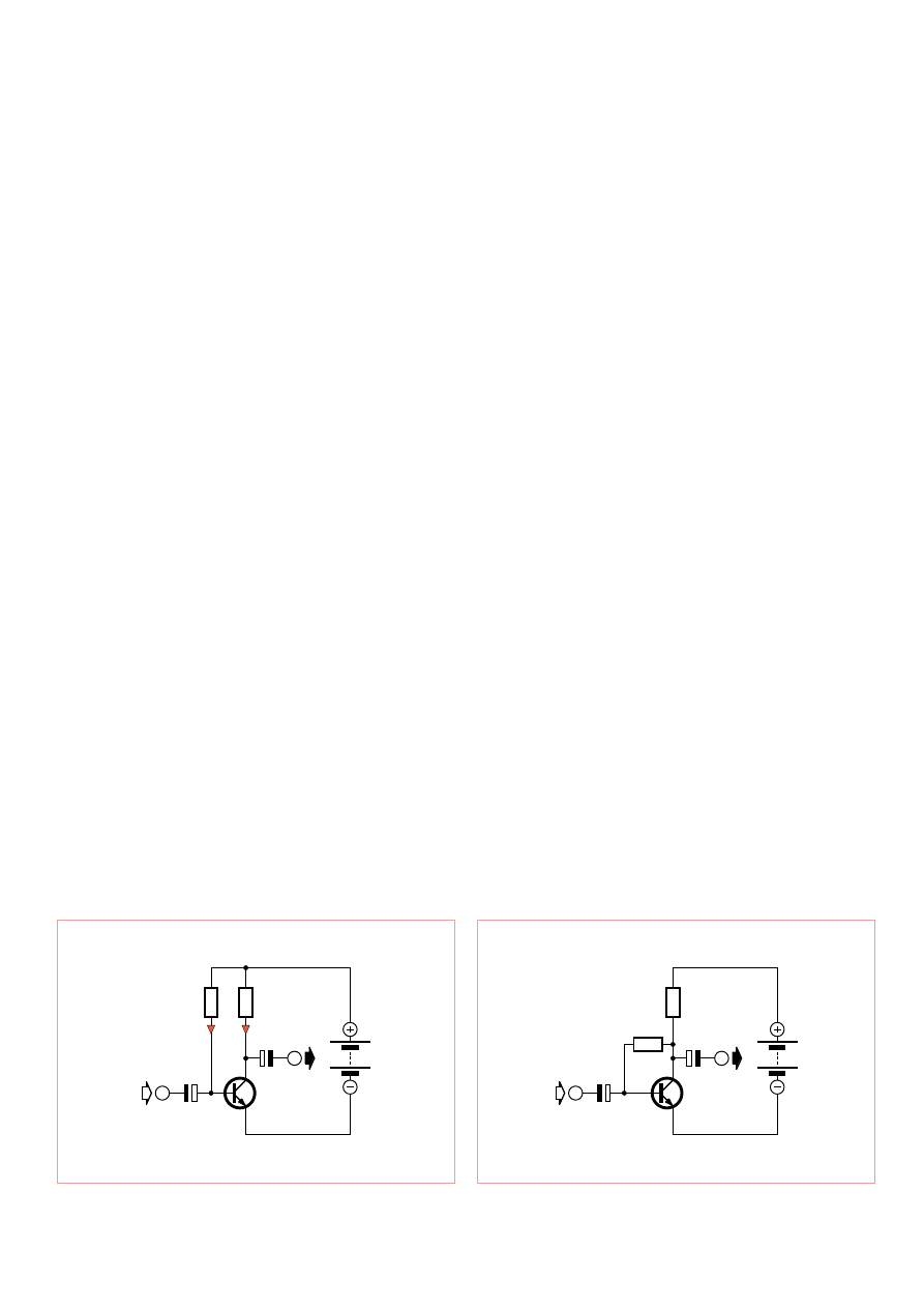
60
10-2012 elektor
BASICS
Electronics for Starters (8)
Audio Preamplifier
The principle of a (preferably) linear ampli-
fier is straightforward: an audio signal mod-
ulates (varies in volume and frequency) the
small base current of a transistor, so that the
amplified collector current produces cor-
responding audio signals of greater inten-
sity. The most commonly employed ampli-
fier circuit is the emitter circuit, the name
implying that the emitter is connected to
the common ground potential of the cir-
cuit. Whilst the base voltage and collec-
tor voltage can vary, the emitter voltage
always remains constant, namely 0 V. In cir-
cuit diagrams we sometimes draw compo-
nents with individual ground symbols and
at other times a continuous ground connec-
tion, but the meaning is the same. Gener-
ally the ground connection is joined to the
minus (negative) pole of the current source.
Our goal for an amplifier of this kind is to
provide the greatest possible dynamic
range before distortion occurs and under-
mines the satisfyingly faithful amplification
achieved up till then. For this reason the qui-
escent collector current should be capped
at just half the maximum possible current,
with the collector resistor and supply volt-
age selected carefully to achieve this. In this
way the current can be varied significantly
in either direction to an equal extent with-
out hitting limitations. All the same, achiev-
ing the correct quiescent current with a
suitable base resistor is not entirely simple.
If we take a look at Figure 1, we see here
some optimal values for the components,
assuming that the BC547B transistor hap-
pens to exhibit current amplification of
exactly 300-fold. The base current amounts
to
I
B
= U / R = (9 V – 0.6 V) / 560 kΩ = 15 µA.
The collector current is then I
C
= I
B
× V =
15 µA × 300 = 4.5 mA. The voltage dropped
across the collector resistor is U = I × R =
4.5 mA × 1 kΩ = 4.5 V. The remainder of
the 9 V, also 4.5 V as it happens, is devel-
oped between the emitter and collector.
This is the ideal case, in which the output
can now be driven an equal extent in both
directions. The voltage on the collector
can therefore vary between 0 V and 9 V,
meaning for example that a pure sinewave
tone will be amplified at maximum output
voltage without distortion. The voltage
amplification is in this situation more than
100-fold.
However, if you build this circuit using a
variety of transistors you will get a differ-
ent result each time, because their current
gain varies wildly. In the åworst-case sce-
nario, a transistor might have an amplifica-
tion factor of 600, which is so great that the
transistor is already switched hard-on
to full
saturation
. Then you can forget about get-
ting low-distortion output signals. Fortu-
nately there is a perfect remedy: negative
feedback.
Negative feedback
The simplest form of negative feedback
occurs when the base resistor is connected
not to the supply voltage but to the collec-
by Burkhard Kainka (Germany)
One of the most important applications for transistors is the amplification of audio signals. The
device providing this function is the audio amplifier or audio frequency (AF) amplifier. This might be a
microphone preamplifier or perhaps part of a radio circuit but the result is the same: something quiet
is made louder!
9V
1k
BC547B
10u
560k
10u
15uA
4mA5
V = 300
9V
1k
BC547B
10u
270k
10u
Figure 1. Setting the bias point for exactly 300-fold gain.
Figure 2. Setting the bias point with negative feedback.
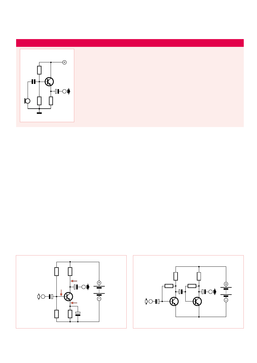
61
elektor 10-2012
ElECtronICS for StArtErS
tor (Figure 2). The rule of thumb is this: R
B
= R
C
× V, where V is selected for the middle
range of current amplification expected. For
300-fold current amplification and a collec-
tor resistance of 1 kΩ we need to use a base
resistor of around 300 kΩ.
This time our circuit reacts in a more meas-
ured manner to differing current gain situ-
ations. Greater gain leads to larger collec-
tor current and therefore to greater voltage
drop across the collector resistor. The col-
lector-emitter voltage falls at the same time
and with it the voltage on the base resistor
too, which in turn leads to a reduction in
base current. The nett result is higher gain
offset in part by smaller base current, so
that the collector current rises less. We call
this negative feedback because the increase
in collector current is counteracted. In this
situation the negative feedback leads to
reduced amplification but with correspond-
ingly less distortion. Most importantly, you
can use absolutely any NPN transistor in
your junk box to build this circuit and it will
work each and every time. Or expressed
more scientifically, the circuit can tolerate
a wide variation of samples.
Achieving a still more accurate setting of
the bias point calls for more effort. For this
purpose we provide the transistor with an
emitter resistor (Figure 3). By providing the
base with a voltage divider we can ensure a
fixed voltage on the base, in which the cur-
rent flowing through the voltage divider is
around 10 times larger than the base cur-
rent, thus avoiding any reaction arising
from variations in base current. The emitter
voltage stabilises itself at a value in which
the base-emitter voltage is below the base
voltage. This means the emitter current
remains stable and consequently the col-
lector current too.
In the sample circuit a base voltage of 3 V
is given. This determines the emitter volt-
age of 2.4 V. An emitter resistor of 1 kΩ
produces an emitter current of 2.4 mA. A
collector resistor of 1 kΩ causes a voltage
drop of 2.4 V. The resulting collector volt-
age is 6.6 V, along with a collector-emitter
voltage of 4.2 V.
The circuit displays a strong relationship
between voltage and negative feedback.
A small variation in the emitter voltage has
a direct effect on the base-emitter voltage
and, on account of the steep characteris-
tic curve of the base, leads to a significant
change in the collector and emitter cur-
rents. Since only very small variations in
base-emitter voltage are desired, the emit-
ter voltage is set at a value that is always
about 0.6 V below the base voltage. The
function resembles that of the so-called
emitter follower (see panel).
9V
1k
BC547B
10u
22k
10u
6V6
1k
3V
11k
100u
2V4
9V
1k
BC547B
47u
10k
1u
270k
10u
2M2
BC547B
Figure 3. Stabilising the bias point.
Figure 4. A two-stage audio amplifier.
The Emitter Follower
The emitter follower is also
known as the common col-
lector circuit, as the transis-
tor operates with a constant
collector voltage. The output
of the amplifier is at the emit-
ter. Every change of volt-
age on the input is reflected
automatically at the output
because even a very small
variation in the base-emitter
voltage is sufficient to alter
the emitter current signifi-
cantly. The emitter voltage
lies always around 0.6 V below the base voltage.
A change in the base voltage of 1 V is therefore reflected in one of
almost 1 V in the emitter voltage as well. The precise value might be
0.99 V if a change in collector current required a variation in base-
emitter voltage of 10 mV. The voltage amplification is thus almost
unity (1), meaning the input voltage is not amplified even though
the input current certainly is. The advantage of the emitter follower
is its high input resistance or impedance. Wåhilst the input resist-
ance of an emitter follower circuit is about 1 kΩ (according to its bias
point), the collector circuit achieves 100 kΩ and more. For example,
you can connect a crystal microphone or a crystal pick-up cartridge
direct. This circuit also lets you use a simple piezo-ceramic transduc-
er as a microphone (or for picking up sound waves in solid objects). It
can be used like this for monitoring pulse beats for instance.
4k7
BC547B
10u
470k
+9V
470k
100n
R
i
= 100k
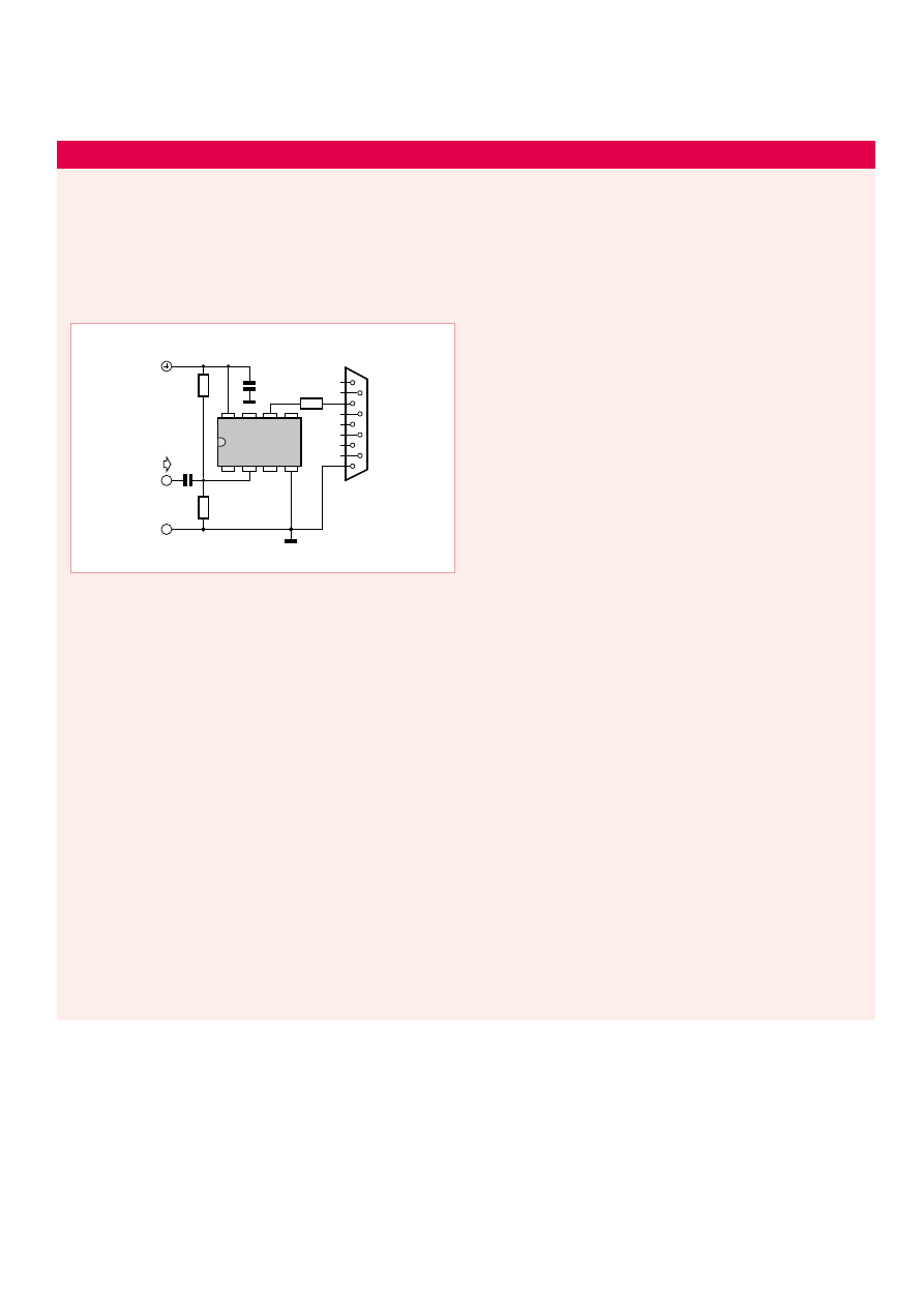
62
10-2012 elektor
BASICS
In principle a harsh level of negative feed-
back has the disadvantage of much reduced
voltage amplification. To achieve adequate
amplification of audio signals we need to
boost the negative feedback for AC cur-
rents, specifically by using an emitter capac-
itor. Its value is determined by the lowest
frequency being handled, without skimping
(avoid using too small a value).
Two stages
If the level of amplification provided by a
single transistor is insufficient, a multi-stage
amplifier will be required. Figure 4 shows a
version with two stages and R-C coupling.
In most situations the simple form of neg-
ative feedback, with one resistor between
base and collector, will be entirely adequate
for obtaining an appropriate bias point. The
circuit also demonstrates a further prin-
ciple of amplifier development: from left
to right, the circuit becomes successively
lower in impedance. In this way we achieve
high input resistance and low output resist-
ance. The latter would not be up to connect-
ing a loudspeaker but with headphones
on the output, it would be fine for many
applications.
An audio millivoltmeter
An audio millivoltmeter would be very handy for investigating the
amplifiers described here. The A-D converter in the ATtiny13 can in
fact measure only DC voltages. All the same, by elevating the mean
voltage to 2.5 V and making rapid measurements, AC voltages can
be investigated as well. The result is sent serially to the PC and can
then be displayed using a terminal program.
The principle of the measurement program is straightforward. First
we determine the mean voltage by averaging. There then follows
a rapid series of multiple individual measurements, from which the
mean voltage is subtracted, creating an absolute value for each in-
stance. The smallest measurable voltage step for the A-D converter
is actually 5 mV. Even so, by averaging many separate readings we
can get down to 1 mV. In the actual measurement loop process we
carry out, process and add up 2,780 readings. Incidentally, the read-
ing points are entirely asynchronous with regard to the test signal.
However, the large number of test measurements made and the ran-
dom factor combine to produce an adequate result, so long as the
input signal remains between roughly 50 Hz and 50 kHz.
How do we arrive at this ominous figure of 2,780? This figure is
based on a reference voltage of 5 V and takes into account the dif-
ference between arithmetic averaging and true RMS measurement,
so that the result in the case of a sinusoidal signal is displayed as
actual effective values in mV
eff
. In order to determine accurate rms
(root-mean-square) values, you would have to actually add up the
square of the voltage and afterwards calculate the mean value from
the square root. This would overwhelm the ATtiny13, however. For
this reason we derive the arithmetic mean from the absolute volt-
age. This is around 10% too low, or more precisely by a factor of the
root of 2 divided by pi / 2, i.e. 0.9003. One A-D step is 5000 mV /
1023 = 4.8876 mV. In addition the measured value is multiplied by 8
and then divided by 4096, thus effectively dividing by 512. In order
to display everything correctly in mV, we need to multiply by 512 ×
4.8876 / 0.9003 = 2780, and this is simplified when 2,780 measure-
ments are totalled.
The result is remarkably accurate. Even values like 1 or 2 mV
eff
are
displayed stably!
‘Millivoltmeter 1 mVeff ... 2000 mVeff
$regfile = “attiny13.dat”
$crystal = 1200000
$hwstack = 8
$swstack = 4
$framesize = 4
Dim U1 As Integer
Dim U2 As Integer
Dim U3 As Long
Dim N As Integer
Config Adc = Single , Prescaler = Auto
Start Adc
Open “comb.1:9600,8,n,1,INVERTED” For Output As #1
Do
U2 = 0
For N = 1 To 64
U1 = Getadc(3)
U2 = U2 + U1
Next N
Shift U2 , Right , 3 ‘ /8
U3 = 0 ‘ zero point
For N = 1 To 2780
U1 = Getadc(3)
Shift U1 , Left , 3 ‘ *8
U1 = U1 - U2
U1 = Abs(U1)
U3 = U3 + U1
Next N ‘ * 2780
Shift U3 , Right , 12 ‘ / 4096
Print #1 , U3
Loop
End
100n
100n
1mV...2V
+5V
ATtiny13
VCC
PB2
PB1
PB0
RES
PB3
PB4
GND
470k
1k
470k
1
2
3
4
5
6
7
8
9
RxD
GND
RS232/
PC
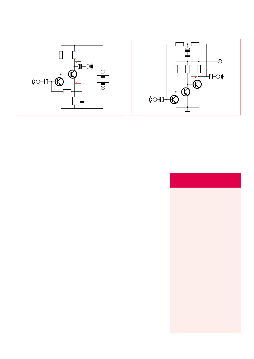
63
elektor 10-2012
ElECtronICS for StArtErS
DC-coupled stages
Multi-stage audio amplifiers can be created
at reduced cost if you forego capacitor cou-
pling between the individual stages and
employ DC coupling instead. The collector
resistor of the first transistor is now simul-
taneously the base resistor of the second
one (Figure 5). Frequently this also simpli-
fies setting the bias point, with the base cur-
rent being appropriate for both transistors.
Figure 5 shows a two-stage, directly cou-
pled amplifier. The base current of the first
transistor is branched off from the emitter
of the second stage. This provides negative
feedback and stabilisation of the bias point.
The voltage drop across the relatively small
base resistor of 100 kΩ can be disregarded
and consequently the emitter voltage at the
second transistor amounts to around 0.6 V.
In the process the emitter resistor of 330 Ω
determines the emitter and collector cur-
rents of the second stage, which are largely
independent of the supply voltage.
The negative feedback should not lead to
any reduction in AC voltage amplification.
An additional emitter capacitor takes care
of ensuring that only DC current is fed back.
In practice the amplifier has a low frequency
limit that can be set even lower with a larger
emitter capacitor.
Three stages
The position is even simpler with a three-
stage amplifier because negative feedback
can be applied direct from the output to the
input (Figure 6). Each stage reverses the
signal phase by 180 degrees. With a two-
stage amplifier we needed a flip-flop to
achieve feedback. On the other hand, one
or three stages produce negative feedback,
which stabilises the bias point.
Figure 6 shows a circuit optimised for small
supply voltages from 1 V upwards. Here, as
in Figure 2, we see how greater amplifica-
tion in the transistors leads to increased
collector current flow in the third transis-
tor and hence to larger voltage drop across
its collector resistor. The collector-emitter
voltage falls and consequently also the volt-
age dropped across the two 100 kΩ nega-
tive feedback resistors. This results finally
in reduced base current, as explained pre-
viously above.
The collector-emitter voltage here amounts
consistently to merely 0.6 V or so, ena-
bling each stage to deliver relatively mod-
est amounts of audio amplification. All the
same, this is more than compensated by the
high number of amplifier stages.
The negative feedback element of the cir-
cuit includes a low-pass filter with a capaci-
tor to ground (bypass capacitor), which
boosts the negative feedback for higher
frequencies. It is essential for achieving high
levels of audio amplification. The circuit is,
for example, ideal as a sensitive microphone
preamplifier or as audio amplifier in simple
radio receivers. A headset can be connected
directly in place of the collector resistor in
the third stage. Incidentally the circuit was
used in the ‘Tapir’ RF Sniffer described in the
Elektor July & August 2012 edition (www.
elektor.com/120354).
(120008)
9V
1k
10u
47k
1u
330R
100k
100u
7V2
BC547B
0V6
2x
1k
47u
100k
1u
BC547B
0V6
10k
+1V5
100k
100k
3x
1u
Figure 5. A two-stage audio amplifier with DC coupling.
Figure 6. A three-stage, direct-coupled amplifier.
Quiz solution from
the June 2012 edition
The correct solution code is ‘CDG’. Here
is how it is worked:
Solution 1:
The LED drops around 1.8 V, with U
CE
at the
transistor about 0.1 V. This leaves 7.1 V
over. 1 kΩ and 470 Ω form a voltage di-
vider of around 3.1:1. 7.1 V / 3.1 = 2.3 V
(Solution C).
Solution 2:
For the left-hand transistor to start conduct-
ing its base voltage must be around 0.6 V
above the emitter voltage, hence 2.3 V +
0.6 V = 2.9 V. The correct solution is D.
Solution 3:
If the right-hand transistor is fully cut off
and the left-hand one is hard on, we will
find approx. 9 V / 11 = 0.8 V at the emitter
resistor. This gives a base-emitter voltage
of 0.6 V, which the left-hand transistor
requires to conduct. Therefore the lower
switching point lies around 1.4 V (G).
64
10-2012 elektor
test & measurement
Vocal Annunciator
How about making
your next project speak?
By Christian Picard (France)
When your attention is occupied elsewhere, it’s sometimes impossible to
watch a display — to keep an eye on a changing value, for example. Here’s just
one example: you’re keenly watching your favourite R/C model, on the ground
or in the air, which just happens to be fitted with telemetry. Now wouldn’t it
would be a great idea if you could keep track of its speed or altitude, or the
drive battery voltage, just by listening. What do you say to that?
Module description
The voice of the whole thing comes from a module by 4D Systems,
the SOMO-14D [1], which is capable of reading files from a micro SD
memory card of 2 GB maximum. The module’s audio output can be
to a speaker or headset.
As for the brain of this project, that’s an Atmega8AU microcon-
troller, clocked by an 8 MHz crystal, whose mission is to drive the
sound module that is going to perform the voice playback of the
number or message analysed. The sound module is driven via a
2-wire (data and clock) serial connection, managed by the micro-
controller which receives its own orders as a slave on the I²C bus.
This circuit will be connected to the I²C bus of an application
and will make it possible, for example, to read out loud a string
of ASCII characters representing a whole or floating-point num-
ber, positive or negative, resulting from a calculation and stored
in a ‘string’ variable.
It is possible to use the SOMO module directly within an application
by using the 2-wire bus —– for example, just for playing sound files —
but this would tie up the main program and memory space, which
may be at a premium in any case if the microcontroller is being used
in ‘lean’ mode! A further advantage of the unit described here is its
transportability to another application.
Firmware
The microcontroller’s main program consists of little more than a
wait loop that analyses the string received as soon as the whole of
the I²C data frame has been decoded. Within this loop, the received
characters trigger an interrupt per character. The program will
leave the loop at the end of the string, indicated by the ‘null’ char-
acter $00, followed by two hex characters representing the num-
ber (name) of the file in the micro SD card containing the units of
the measurement value that has just been read out (or any other
message).
Some clarification may be in order here. Let’s suppose that the num-
ber to be read out is –235.12 V. The ASCII data string to be transmit-
ted is assembled as follows (hexadecimal): $2d $32 $33 $35 $2c $31
$32 $00 $00 $69. Now you’ll have recognized the minus sign in the
character $2d and the comma, $2c. I’m sure you’ve followed the
rest, except perhaps for the last two. Remember, there’s a unit to
be read now: ‘volt’. In point of fact, $00 $69 (= 105 in decimal) is the
number of the file “volt” on the micro SD card. Note that this applies
to the author’s own files — it may well have a different number in
your system, since it’s up to you to record your own sound files.
Returning to the analysis, the first check is to determine if the
received string corresponds to a number or a direct address to the
SOMO-14D module. If the first character received is the null charac-
ter ($00), the program treats the next two hex bytes as a file num-
ber and this file is read. If the first character is not the null charac-
ter, the string is taken as an ASCII representation of a number. In
this case, the programme looks to see if it is a whole number, a
decimal, positive or negative, how many digits before the decimal
point, how many after it (1, 2, or 3 digits maximum), etc. These lat-
ter elements will determine which of the various subroutines will be
called. Among the bytes received that are neither numbers nor file
numbers, there may be direct commands to the sound module, for
example adjusting the volume ($FF $F0 to $FF $F7).
A minor adaptation will be necessary for using English (or other lan-
guages), just for the numbers. For example, the specific differences
between the French and English language way of expressing “hun-
dreds” (FR: cent, EN: one hundred) and “thousands” (FR: mille, EN:
one thousand). Also, the decimal point should replace the comma.
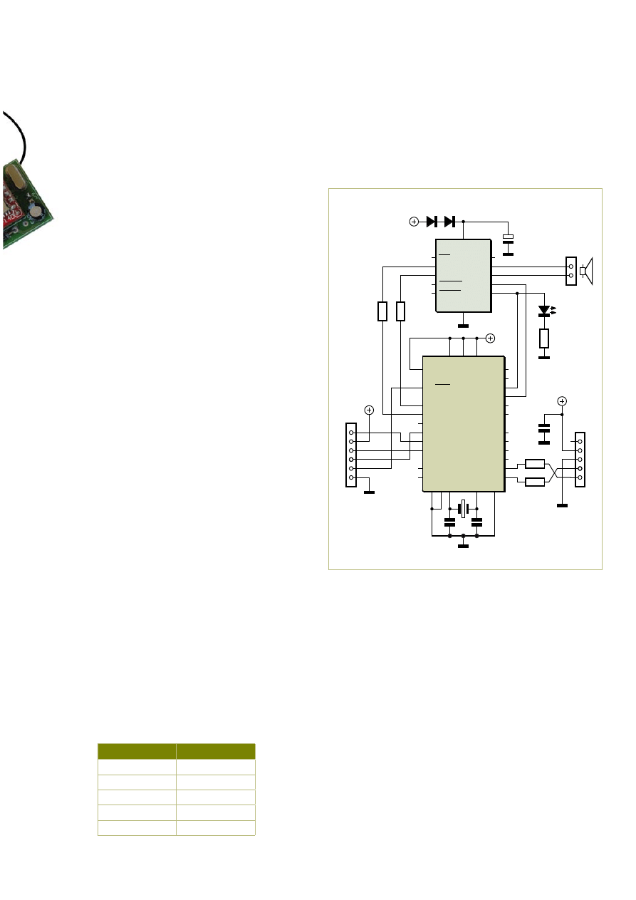
65
elektor 10-2012
Vocal annunciator
It’s a subtle point, but does justify a slight modification in the
structure of the software.
To note…
– Leading non-significant zeroes in the string will be suppressed.
– If the string starts with a zero (ASCII $30), the number will be
interpreted as being less than one and a maximum of three digits
after the decimal point will be read.
– When a number is zero, the string will be $30 $00.
– For a number with no units, the null character at the end of the
string will be followed by $C0, so no unit will be spoken and the
sound display will be stopped.
A few examples (after adaptation to English)
12 will be read out as “twelve”.
527 will be read out as “five hundred twenty-seven”.
13,689,222 will be read out as “thirteen million six hundred eighty-
nine thousand two hundred twenty-two”.
0.155 will be read out as “zero point one hundred fifty-five”
−0.155 will be read out as “minus zero point one hundred fifty-five”
Circuit
The project circuit diagram is shown in Figure 1. The module is rela-
tively compact (25 × 40 mm) and should be easy to fit into applica-
tions. Constructing the board takes a bit of dexterity, but not too
much. Manual soldering of the ATmega8AU (SMD type in a TQFP32
package) is made easier by using solder paste, the same as is used
for reflow soldering. Here’s the method I use: the IC is positioned
accurately and held in place using a spring clip, then a moderate
amount of paste is applied to the IC pins. A fine-tipped soldering
iron will do the job with no risk of bridging between pins.
There’s space for an HE6 socket to allow the microcontroller to be
programmed.
A few resistors and capacitors in SMD packages are required. The two
1N4001 diodes (D2 and D3) are recommended by the manufacturer
to allow the sound module to be powered from 5 V (rated at 3.3 V).
The module can be soldered directly into the board, or mounted by
means of IDC socket strips.
The output at J9 is intended to drive a speaker or headset of 8, 16,
or 32 Ω; the sound module is capable of supplying up to 250 mW.
D4, a 3 mm LED, shows when the SOMO module is busy.
Communication with the I²C bus can be achieved by hard-wiring or
SIL strip connectors.
The pin assignments for J11 are as follows:
Pin
Function
1
not connected
2
+5 V
3
0 V
4
SCL
5
SDA
Everything’s stored in the micro SD card
The memory contains the files required for making up numbers and
messages. The relatively high capacity of the micro SD memory,
2 GB maximum, means it can be used in various different fields.
Around 105 files are needed to produce numbers in French. So
that leaves the user with 407 files that can contain various units,
words, phrases, music, alarm messages for the widest range of
applications.
I²C commands
The module’s address is $58. The access protocol is standard, a
START followed by the module address, then the data representing
the characters of the string to be processed, ending with a STOP
command.
I haven’t tested all the direct commands. The command for setting
the volume has been validated, along with the direct addressing of
the sound files.
X2
8MHz
C16
22p
C17
22p
+5V
J10
1
2
3
4
5
6
+5V
J11
1
2
3
4
5
+5V
R6
470R
R7
470R
R8
300R
R9
300R
C18
100n
PB3/MOSI/OC2
PC4/ADC4/SDA
PC5/ADC5/SCL
PB2/SS/OC1B
PC6(RESET)
PD4/T0/XCK
PB0/ICP1
PB1/OC1A
PB4/MISO
PC0/ADC0
PC1/ADC1
PC2/ADC2
PC3/ADC3
PD2/INT0
PD3/INT1
PD6/AIN0
PD7/AIN1
PB5/SCK
PD0/RXD
PD1/TXD
ATMEGA8
PD5/T1
32 PIN
XTAL1 XTAL2
AREF
U4
AGND
AVCC
GND
VCC
GND
VCC
PB6
PB7
20
21
18
12
29
13
14
15
16
17
23
24
25
26
27
28
30
31
32
10
11
8
7
3
4
5
6
1
2
9
J9
1
2
D3
1N4001
D2
C15
220u
STOP/PLAY
SOMO-14D
PREVIOUS
AUDIO
RESET
U3
DATA
BUSY
NEXT
SPK–
SPK+
GND
VCC
CLK
14
12
11
10
9
8
3
4
5
6
7
1
D4
R10
470R
2x
+5V
110465 - 11
MISO
VCC
SCK
MOSI
RST
GND
ISP
NC
+5V
0V
SCL
SDA
Figure 1. Circuit diagram for the Vocal Annunciator.
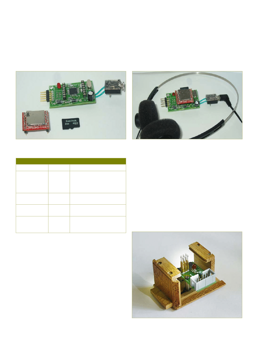
66
10-2012 elektor
test & measurement
SOMO-14D commands according to the manufacturer’s data.
Command code
Function
Description
0000h – 01FFh
Audio file
number
Addresses one of the pre-
recorded audio/sound/voice files
in the micro SD memory card
(from 0 to 512 files max.)
FFF0h – FFF7h
Volume
Code for setting the volume, 8
levels in all.
FFFEh
Play/pause
Plays or pauses the current audio
file.
FFFFh
Stop
Stops playing of the current audio
file and puts the module into idle
mode.
File details
The elementary files in French used by the analysis program may be
downloaded from [2] – they are all ready for loading into a micro
SD card. However, users can create their own messages and the ele-
mentary files can be replaced by these user files.
The elementary files represent the figures from “zero” to “hundred”,
“thousand” (0101d), “mega” (0144d), “comma” (0129d), “point”
(0130d) and “minus” (0102d). Because of the requirements of the
software, the figures from 0 to 99 will occupy files 0 to 99, which
will be converted into hex characters by the software in order to
address the sound module. This behaviour only applies to the part
involving the reading of the numbers, since as explained above, the
direct message commands will be sent in hex.
The voices used can be synthesized or recorded live. The only vital
point is that recordings must have a minimum length in order for
them to be recognized, as the SOMO module will simply ignore files
that are too short.
You can download a free utility (SOMO Tool) [3] from the manufac-
turer’s website, which lets you convert .wav or .mp3 sound files into
.ad4, the only format the SOMO module can recognize.
The manufacturer warns that certain micro SD cards are not suita-
ble. The author uses SanDisk cards, which up till now I’ve found per-
fectly satisfactory, as long as you respect the minimum file length.
(110465)
Internet links
[1] SOMO module: www.4dsystems.com.au/prod.php?id=73
[2] Software and author’s sound files (in French):
www.elektor.com/110465
[3] SOMO audio converter utility:
www.4dsystems.com.au/prod.php?id=74
The main components of the Vocal Annunciator.
For small circuits, fitting a programming connector can be
awkward. To get round this problem, the author has created this
programming device.
The assembled circuit.

Design Simulate Download
Create complex electronic systems
in minutes using Flowcode 5
Convince yourself.
Demo version, further
information and ordering at
www.elektor.com/fl owcode
Flowcode is one of the World’s most advanced
graphical programming languages for micro-
controllers (PIC, AVR, ARM and dsPIC/PIC24).
The great advantage of Flowcode is that it allows
those with little experience to create complex elec-
tronic systems in minutes. Flowcode’s graphical
development interface allows users to construct a
complete electronic system on-screen, develop a
program based on standard fl ow charts, simulate
the system and then produce hex code for PIC
AVR, ARM and dsPIC/PIC24 microcontrollers.
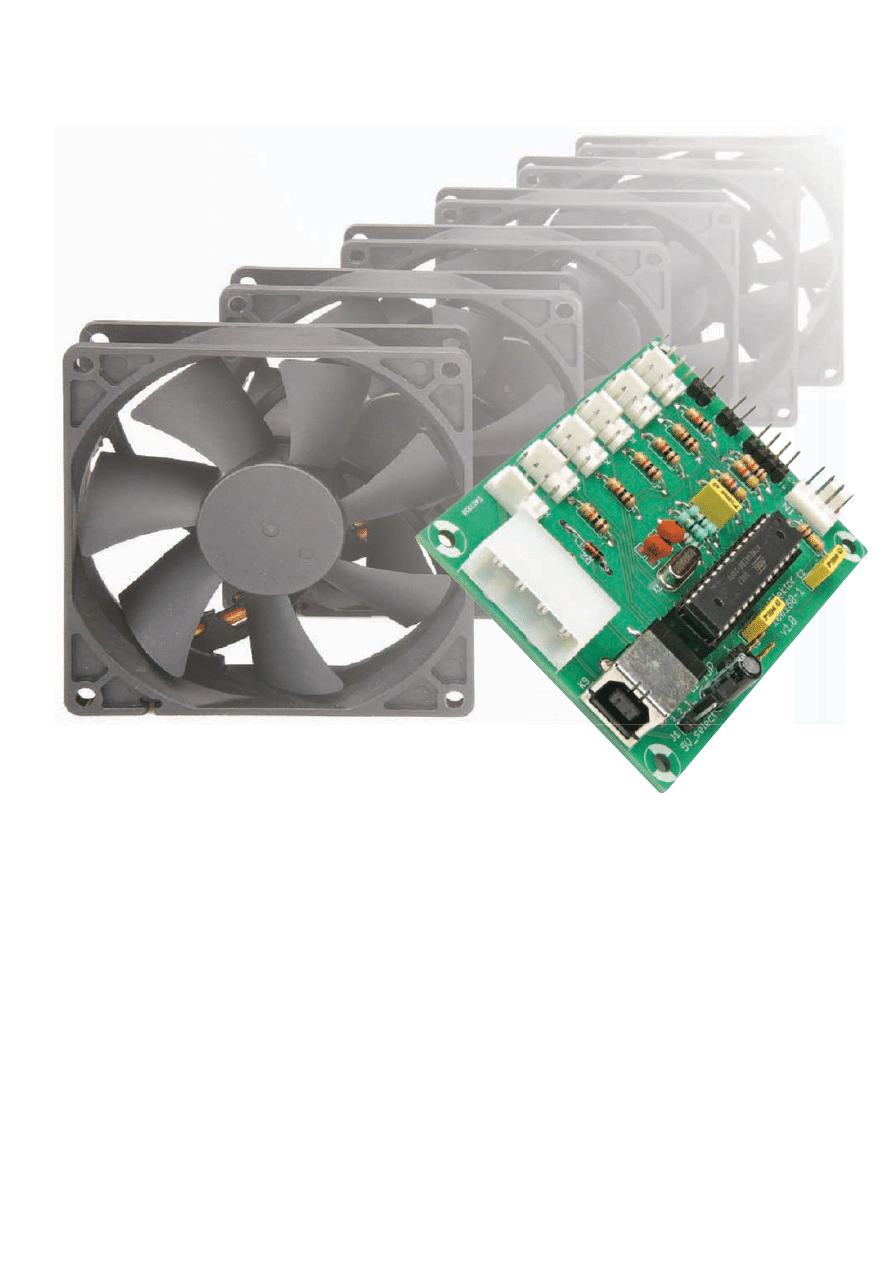
68
10-2012 elektor
Computers
Intelligent
PC Fan Controller
A number of years ago Intel created a spec-
ification for 4-wire PWM driven PC fans
(see [1]). These fans are hardly more expen-
sive than the well-known 2-pin and 3-pin
varieties, although they have the advantage
that their rotational speed can be controlled
using a PWM signal. The 3-pin and 4-pin
connectors also include a tachometer signal
that can be used to feed the instantaneous
speed of the fan back to the motherboard.
A PC motherboard often has only a single
fan connector that includes a PWM signal,
although a PC usually contains several fans.
There is no choice but to run these other
fans at a fixed speed. And even if there is a
facility to connect several PWM fans, it usu-
ally isn’t possible to control them individu-
ally from the motherboard.
By Ivo Pullens (The Netherlands)
In a modern PC you will find a number of fans for removing the heat that is generated. These can’t always
be controlled individually by the PC motherboard. With the help of the circuit described here you can
actively control up to six fans, while the temperature can be measured in various places inside the PC case
using a number of sensors. A PC program is used to configure and monitor the fans, which communicates
with the fan control board via a USB link.
Controls a maximum
of 6 pWm fans
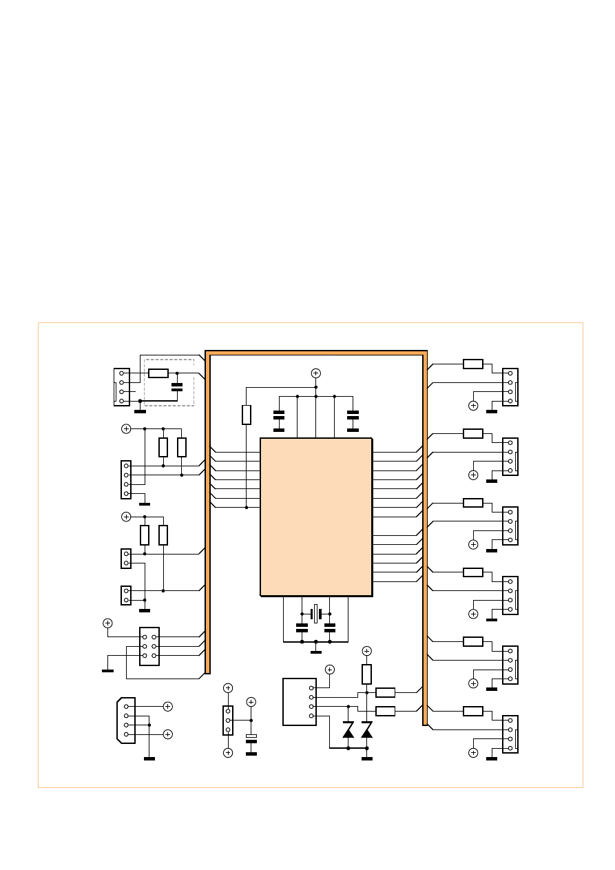
69
elektor 10-2012
Computers
The circuit described here is capable of con-
trolling the speed of up to six fans in a PC
in a safe and flexible manner, so that they
will run at their minimum required speed
and hence keep the noise level as low as
possible.
The circuit
It can be seen from the circuit diagram
in Figure 1 that the circuit itself is very
straightforward. It consists of not much
more than an Atmega microcontroller and
a number of connectors for connecting the
fans, sensors, USB and power supply. The
4-wire fans are connected directly to the
microcontroller, since they are able to cope
with the generated PWM signals without
any further processing. The internal pull-
ups of the microcontroller make sure that
the open-collector tachometer signals from
the fans are pulled towards the positive sup-
ply voltage.
R3/C2 is a low-pass filter that smoothes
(integrates) the incoming PWM signal
from the motherboard, so that an ana-
logue input of the microcontroller can be
used to read the PWM control signal from
the motherboard.
For the analogue temperature sensors you
can use two 10 kΩ NTC sensors, which are
connected to K11 and K12. Together with
the NTCs, R8 and R9 form two potential
PD3(INT1/OC2B/PCINT19)
PD6(AIN0/OC0A/PCINT22)
PB0(ICP1/CLKO/PCINT0)
PB3(MOSI/OC2A/PCINT3)
PD5(T1/OC0B/PCINT21)
PD4(T0/XCK/PCINT20)
PB2(SS/OC1B/PCINT2)
PC6(RESET/PCINT14)
PC2(ADC2/PCINT10)
PC3(ADC3/PCINT11)
PC4(ADC4/PCINT12)
PC5(ADC5/PCINT13)
PD2(INT0/PCINT18)
PD7(AIN1/PCINT23)
PC0(ADC0/PCINT8)
PD0(RXD/PCINT16)
PC1(ADC1/PCINT9)
PD1(TXD/PCINT17)
PB1(OC1A/PCINT1)
PB4(MISO/PCINT4)
PB4(SCK/PCINT5)
ATMEGA168PA-PU
XTAL1
XTAL2
IC1
AREF
AVCC
AGND
GND
VCC
PB6
PB7
23
21
20
22
10
24
25
26
27
28
11
12
13
14
15
16
17
18
19
2
8
7
9
1
3
4
5
6
X1
16MHz
C3
22p
C4
22p
C6
100n
C5
100n
+5V
R4
10k
R6
4k7
R7
4k7
+5V
DUTY_AN_IN
SENSE_IN
TEMP_AN0
TEMP_AN1
SDA
SCL
RESET
SDA
SCL
K10
1
2
3
4
K11
2
1
K12
2
1
TEMP_AN0
TEMP_AN1
R8
10k
R9
10k
+5V
K7
1
2
3
4
R3
100k
C2
100n
SENSE_IN
DUTY_AN_IN
K1
1
2
3
4
R10
1k
K9
+5V
GND
D–
D+
1
2
3
4
Mini-USB
R2
68R
R5
1k5
D2
3V6
D1
3V6
+5V
+5V
USB
+12V
K2
1
2
3
4
R11
1k
+12V
K3
1
2
3
4
R12
1k
+12V
K4
1
2
3
4
R13
1k
+12V
K5
1
2
3
4
R14
1k
+12V
K6
1
2
3
4
R15
1k
+12V
R1
68R
TACHO0
TACHO1
TACHO2
TACHO3
TACHO4/MISO
TACHO5/SCK
K8
1
2
3
4
+12V
+5V
PWR
1
2
3
J1
+5V
PWR
+5V
USB
C1
10u
+5V
USB_D+
PWM0
USB_D-
PWM1
PWM2
PWM3
PWM4
PWM5/MOSI
100160 - 11
PWM0
TACHO0
PWM1
TACHO1
PWM2
TACHO2
PWM3
TACHO3
PWM4
TACHO4/MISO
PWM5/MOSI
TACHO5/SCK
USB_D-
USB_D+
K13
1
2
3
4
5
6
TACHO4/MISO
TACHO5/SCK
RESET
PWM5/MOSI
+5V
LOW PASS, 16Hz
FAN IN
I
2
C TEMP SENSOR
10k NTC CONNECTORS
ISP
PSU
CONNECTOR
5V
SELECT
Figure 1. The circuit consists mainly of an Atmega microcontroller and a large number of connectors.
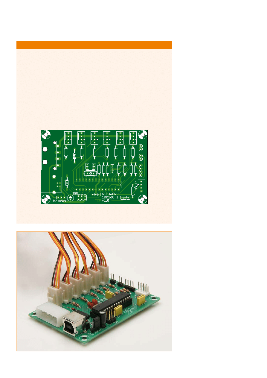
70
10-2012 elektor
Computers
dividers that are connected to ADC2 and
ADC3 of the microcontroller.
If you wish, you can connect a maximum of
eight I
2
C temperature sensors to K10. R6
and R7 are the required pull-ups on the bus.
The firmware has been tested with Micro-
chip MCP980x sensors, but similar sen-
sors such as the TCN75 should work either
directly or with a small modification. When
the firmware starts it figures out itself how
many sensors are connected to the I
2
C bus.
Jumper J1 is used to select either the USB
bus or the PC as the source of the power
supply for the microcontroller. During
firmware development, when no fans are
connected, it can be convenient to power
the circuit via the USB bus, but normally
the PC supply would be used (jumper on
pins 2 and 3).
Construction
Since the circuit doesn’t have any SMDs the
construction is quite easy, especially if you
use the PCB designed for this project (Fig-
ure 2). The large connector (K8) is the male
version of the well-known PC hard drive
connector, made by Molex. If required, the
power supply cable could also be soldered
directly to the board.
The official 4-pin fan headers (K1 to K7) may
be difficult to get hold of in small quantities.
The 3-pin version, however, is much more
widely available. The form and connec-
tions of both connectors are identical, so
that 3-wire fans can be connected to 4-pin
headers. Conversely, if you mount a 3-pin
fan header and in the space for the fourth
pin mount a single header pin you end up
with the equivalent of a 4-pin header (see
Figure 3). This makes it easy to connect
PWM fans without the risk of connecting
them the wrong way.
Firmware
The software for the microcontroller is writ-
ten in C and makes use of a software-based
USB stack V-Usb (see [2]) to communicate
with a PC. The software was initially devel-
oped for an ATmega88, but this was soon
found to be too small to accommodate al
the functions it was required to perform.
For this reason we changed over to the
ATmega168, which has double the amount
of flash memory. However, it is still possible
COMPONENT LIST
Resistors
R1,R2 = 68Ω
R3 = 100kΩ
R4,R8,R9 = 10kΩ
R5 = 1.5kΩ
R6,R7 = 4.7kΩ
R10-R15 = 1kΩ
Capacitors
C1 = 10µF 16V radial, lead pitch 2.5mm
C2,C5,C6 = 100nF, lead pitch 5mm
C3,C4 = 22pF
Semiconductors
D1,D2 = 3.6V zener diode, 400mW
IC1 = ATmega168PA-PU, programmed,
Elektor # 100160-41
Miscellaneous
X1 = 16MHz quartz crystal
J1 = 3-pin pinheader with jumper
K1-K6,K7 = 4-pin fan header
K8 = 4-pin PC supply plug, PCB mount
K9 = Mini USB-B connector, PCB mount
K10 = 4-pin pinheader
K11,K12 = 2-pin pinheader
K13 = 6-pin (2x3) boxheader
PCB # 100160-1 [3]
Figure 2. With this PCB the construction of the circuit becomes child’s play!
1
4
1
2
3
1
6
K9
R
2
R
1
R
5
D
1
D
2
IC1
X1
C
3
C
4
C
5
C6
K8
C1
K1
0
R
6
R
7
K1
1
K1
2
R
8
R
9
R
10
R
11
R
12
R
13
R
14
R
15
R
3
C2
R
4
J1
K1
K2
K3
K4
K5
K6
K7
K13

71
elektor 10-2012
Computers
to compile the software for the ATmega88,
although with a reduced functionality (refer
to the file config.h in the download available
from the Elektor website [3]).
As mentioned in the Intel specification for
4-wire fans, they should be controlled with
a PWM signal with a frequency of about
25 kHz, where the rotational speed should
follow the duty cycle linearly from 20%
upwards (at lower duty cycles the speed is
undefined). The ATmega contains six PWM
outputs, but only two of these (which are
driven by the 16-bit Timer1) can be set to
exactly 25 kHz. The other PWM outputs
are driven by 8-bit timers and can be set to
either 7.8 kHz or 62.5 kHz. A little trick is
used to make them operate at the required
frequency. They are set to operate at the
lower frequency of 7.8 kHz, but then the
overflow interrupt of Timer1 is used to
restart the 8-bit timers, which causes all
PWM outputs to operate at 25 kHz.
The pulses from the tachometers, which
are used to measure the rotational speed of
the fans, are counted using the pin-change
interrupt. In practice the fans rarely went
faster than 6000 revolutions per minute,
where the tachometer outputs two pulses
per revolution. When all fans run at full
speed this means that the software has
to deal with about 1200 pin-change inter-
rupts per second. This may seem like a lot,
but the main loop is quite simple which
leaves plenty of time for calculating the
duty cycles.
This main loop checks every second if any of
the fans has stopped, for example because
of a fault or obstruction. Depending on the
settings, a stalled fan can cause the simu-
lated tachometer signal to stop, thereby
signalling to the motherboard that a fan
has stopped. Any function on the mother-
board that raises an alarm when a fan fails
will therefore continue to work.
Next, the current sensor values are read, all
the calculations are carried out and the val-
ues for the duty-cycles are written into the
output-compare registers for the timers.
The interval of one second for calculating
the new duty cycles may seem like quite a
long time in the world of microcontrollers,
but it is quite suitable for controlling a slow-
changing process such as the temperature
inside a PC.
The simulated tachometer signal for the
motherboard has to be able to provide a
maximum of about 1200 pulses per sec-
ond, where the timing doesn’t have to be
that accurate. For this reason the pulses are
generated from the main loop, where the
tachometer pin is made to go alternately in
a low state and a high-impedance state in
order to reproduce the required open-col-
lector output.
With the help of the PC software the cur-
rent configuration for the controller can
be stored in the EEPROM, so that it can be
automatically loaded when the circuit is
turned on again.
A large part of the software consists of the
USB stack and the routines for exchanging
messages with the PC. The ‘realtime’ com-
munication with the PC is taken care of by
the INT0 handler, which has the highest
priority.
Software
The PC software has been written in C++
and was developed using the free Micro-
soft Visual C++ 2010 Express. The graphi-
cal interface makes use of wxWidgets,
which means that it can be used both
under Windows as well as Linux (and OS
X too, but this has not been tested in prac-
tice by the author).
LibUsb has been used to communicate
with the circuit via a USB link. A sepa-
rate library has been used for the creation
and exchange of messages. This hides the
details of the communication between the
PC and the circuit and promotes the re-use
of the routines. From here you can directly
set the rotational speed of fans or read the
sensor values.
The graphical interface consists of the fol-
lowing tabs:
• Admin
Here you can manage the EEPROM, such
as reading or writing the configuration.
Remember to store a good configuration
into the EEPROM at the first opportunity,
otherwise the circuit will have a blank con-
figuration when it restarts!
Specifications
•Autonomous individual control of up to six 4-wire PWM fans.
•Measurement of the rotational speed of these fans and detection
of stalled fans.
•Support for a maximum of 8 sensors to control the fan speed:
- 2 NTCs
- I
2
C temperature sensors, MCP980x/TCN75 compatible
- Rotational speed of fans can also be used as a ‘sensor’ signal
- External ‘sensors’, where the value can be set via USB
- The duty-cycle of an external fan control signal, such as
emanating from a motherboard
•The rotational speed can be set in three ways:
- Constant
- Linear control where the rotational speed
depends on a sensor signal
- PI-controlled that uses a sensor signal and
a required sensor value to calculate the rotational speed
•Configuration and monitoring via USB.
•Software library for use in PC applications to let you
communicate with the circuit and a PC application to configure
and drive the circuit, for Windows as well as Linux.
Figure 3. With the addition of an extra pin
you can use a 3-pin fan header
to make up a 4-pin connector for a
PWM controlled fan.
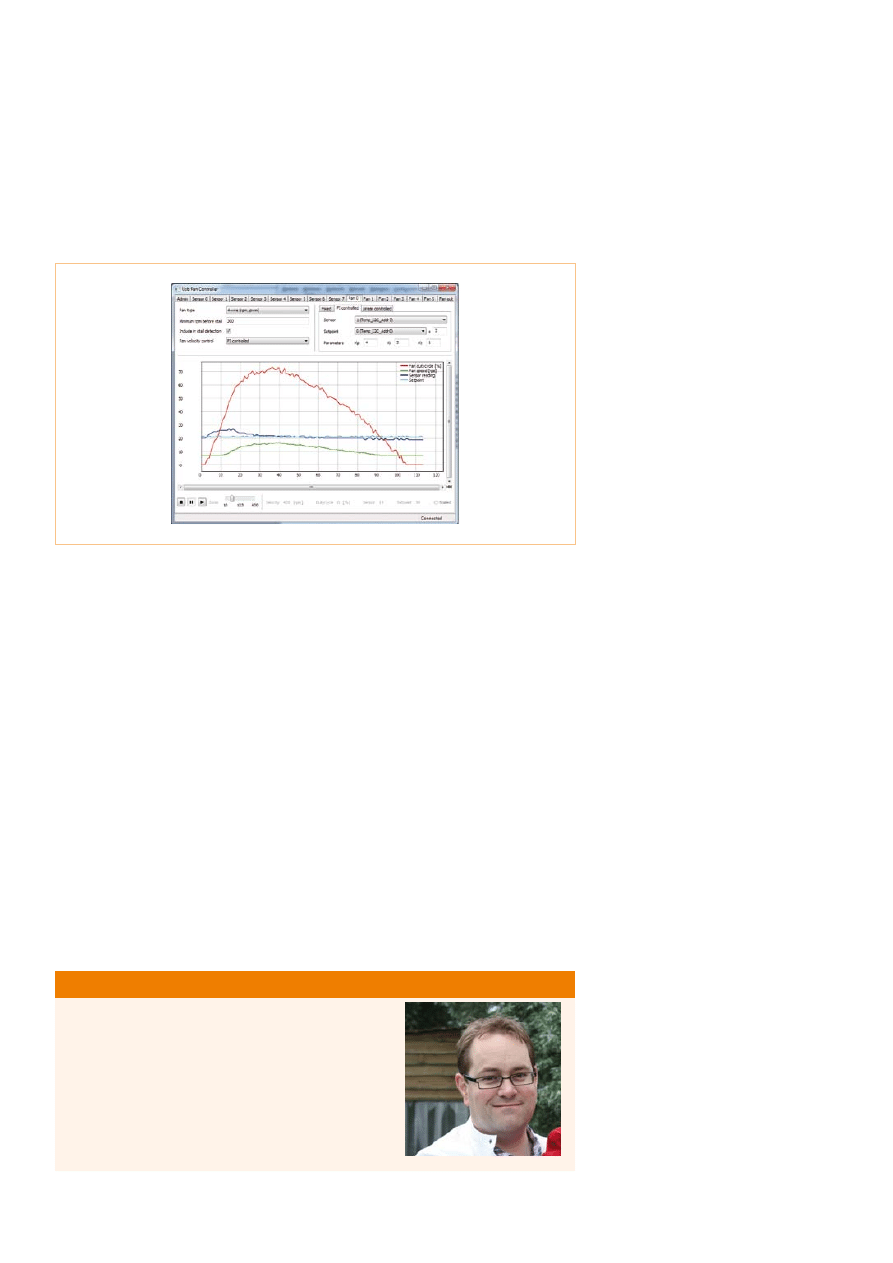
72
10-2012 elektor
Computers
• Sensor0 to 7
The sensor tabs let you assign the con-
nected sensors to a sensor input and inspect
their value graphically over time.
• Fan0 to 5
Here you can configure the individual fans.
• Fan out
This is used to configure the simulated
tachometer signal to the motherboard.
Before a sensor can be used as a controller in
the circuit it needs to be assigned to a sen-
sor input.
Figure 4 shows an example of the configu-
ration for Fan 0, which is connected to K1.
At the top-left the type of fan (so the soft-
ware knows if a tachometer and/or PWM
signal can be used) and the type of con-
trol can be selected. In this example the I
2
C
sensor with address 0 (Temp_I2C_Addr0)
measures the temperature of the outside
air that is sucked into the PC case and the
sensor with address 7 (Temp_I2C_Addr7)
measures the temperature inside the case
itself. Since the PC generates heat itself, it
would be unrealistic to expect to get the
inside temperature the same as the out-
side temperature. The controller will there-
fore be configured such that the inside tem-
perature will be at most 2 °C higher than the
outside temperature (the setting +2 after
the setpoint). The PI (Proportional-Integral)
control selected here continuously calcu-
lates the difference between the required
temperature (outside temperature +2 °C)
and the measured inside temperature. The
controller will increase the rotational speed
of the fan proportionally (using factor Kp)
and also take account of integrating errors
over time (factor Ki).
In the figure you can see that the fan starts
of slowly at a duty-cycle of 0%. When the
inside temperature increases (the dark blue
line) above the required temperature (the
light blue line), the controller ensures that
the rotational speed of the fan increases
(the green line, in revolutions per second).
When the required temperature has been
reached again after some time the rota-
tional speed gradually decreases.
Another possible application for this circuit
is to synchronise the speed of several fans
in order to keep vibrations in the PC case to
a minimum. To do this, use a PI controller
with the rotational speed of one fan as the
sensor for all other fans and negative factors
for Kp and Ki.
On the final tab you can configure the
source for the simulated tachometer sig-
nal to the motherboard, such as the fan
with the lowest rotational speed or a copy
of one of the connected fans. For each fan
a minimum required rotational speed can
be specified. If it falls below this limit the
software considers that the fan has stalled
and the simulated tachometer signal to the
motherboard will be stopped.
In the Elektor download [3] you will find
both the firmware for the microcontroller
as well as the PC software.
(100160)
Internet Links
[1] www.formfactors.org/developer/
specs/4_Wire_PWM_Spec.pdf
[2] www.obdev.at/products/vusb/
index.html
[3] www.elektor.com/100160
About the author
Ivo Pullens is a freelancer who has specialised in embedded
software development.
He recently worked on a large industrial assignment for the
production of semi-conductors and the industrial fieldbus.
In his infrequent spare time he develops solutions to every-
day problems, usually based on microcontrollers.
More information can be found on his website
(in Dutch only):
www.emmission.nl
Figure 4. A screendump of the associated PC program that is used for the
configuration and monitoring of the fans.

If you’ve ever wanted to design and program with the ADuC841
microcontroller, or other microcontrollers in the 8051 family, this is the book
for you. With introductory and advanced labs, you’ll soon master the
many ways to use a microcontroller. Perfect for academics!
Now
Just
$35.00
ADuC841 Microcontroller Design Manual:
From Microcontroller Theory to Design Projects
www.cc-webshop.com
Buy it today!
2 29
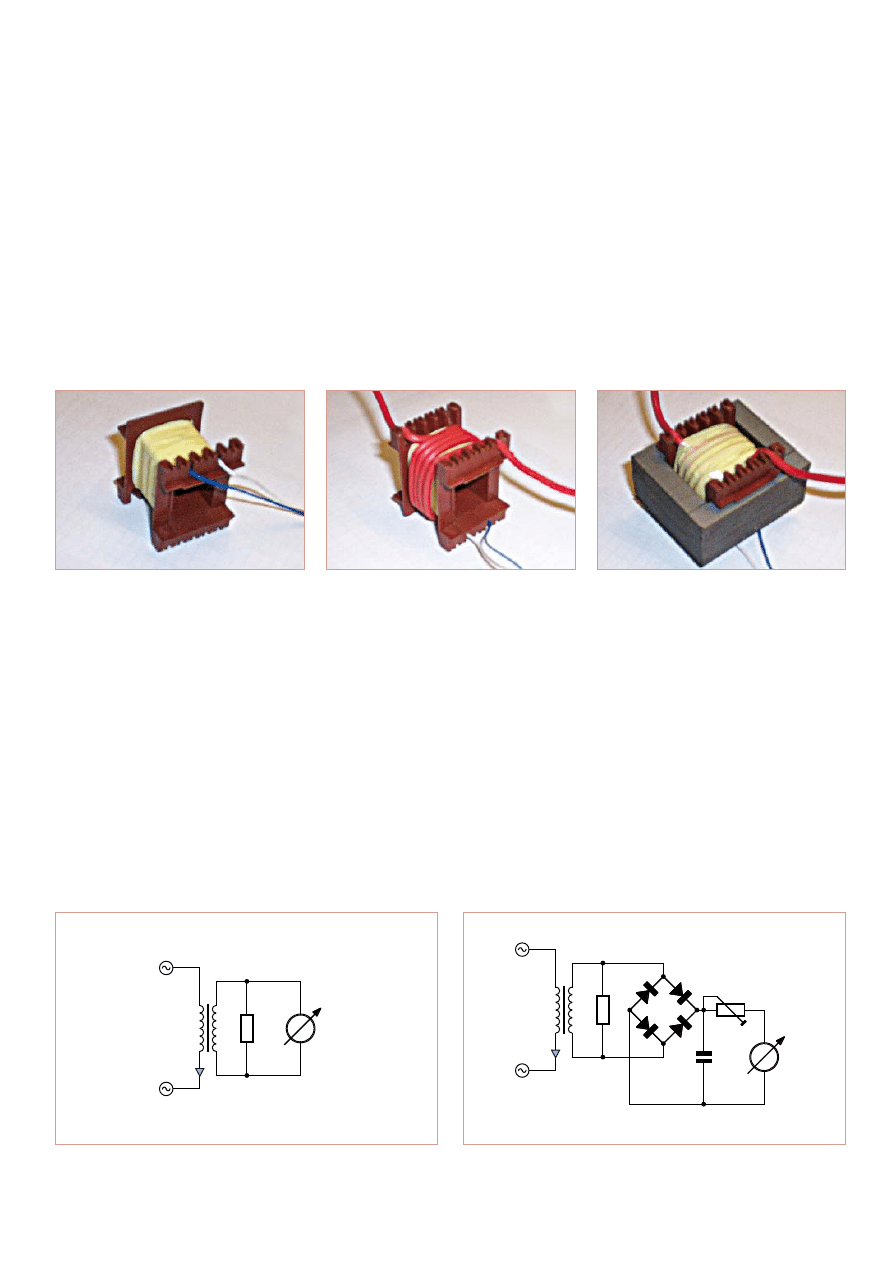
74
10-2012 elektor
Design tip
Current Transformers
Current transformers (CTs), as their name
implies, transform a high current to a
smaller one (usually) for metering and con-
trol purposes. They also provide isolation
between primary and secondary windings;
as such they are used extensively in the
power infrastructure. Their great advan-
tage over more modern devices such as
Hall effect and Rogowski coils is that they
are self powered and will operate meters
and protective relays without additional
supplies.
Setting up parameters
As with all transformer designs, it is cus-
tomary to define the load, or burden, as
it is mostly also known. For most profes-
sional CTs this is usually no greater than
10 VA (loads are often expressed in VA
rather than watts due to phase shifts
being involved; this is not really a con-
cern in the simple designs we introduce
in this article).
For the purposes of this design we will be
driving a meter or feeding a comparator
as part of a protective circuit and a load of
0.5 VA will be sufficient.
We will assume that we wish to monitor the
current in a circuit with a maximum value
of 10 A, and that we want to lower this to
50 mA, i.e. a 200:1 ratio.
With a 0.5 VA load and 50 mA of current we
calculate a voltage of 10 V (U = P / I) and a
resistive load value of 200 ohms (R = U / I).
By Ed Dinning (United Kingdom)
Professional current transformers often use toroidal cores and are wound to high precision. The purpose
of this article is to demonstrate how to make your own current transformers for projects, using readily
available parts. This will allow safe, isolated measurements of current in power supply conductors.
R
L
50mA
AC
10A
max
110323 - 11
R
L
1mA
AC
10A
max
R
C
100n
110323 - 12
Figure 3. Completed and laminated current
transformer.
Figure 4. Test circuit for our self wound transformer.
Figure 5. A CT in a circuit with a moving coil meter.
Figure 2. Current transformer with primary
winding added.
Figure 1. Current transformer with
secondary winding on bobbin.

75
elektor 10-2012
Current transformers
We need to calculate the secondary turns
required to go on the transformer. For this
application we will use a small transformer
that has a core area of, say 300 to 400 mm
2
.
These can be obtained cheaply and even
recovered from old equipment. The larger
the core area, the fewer turns that will be
required.
Many commercial transformer laminations
are classified with an EI number. We are
using an EI48 (long dimension of lamina-
tions equals 48 mm) by a 20 mm stack. The
centre leg of the lamination is 16 mm wide,
and with a stack of 20 mm of these the area
works out at:
0.016 × 0.02 = 0.00032 m
2
.
We then use the transformer equation:
N = E / (4.44 f B A
e
)
where N is the number of turns, E the
applied voltage, f the system frequency, B
the flux density in Tesla and A
e
the cross-
sectional area of the core in square metres.
The AC line frequency is 50 Hz (US: 60 Hz).
It is common to operate at the relatively low
flux density of 0.2 Tesla (unlike a voltage/
power transformer operating at >1 Tesla,
depending on lamination material). Enter-
ing these values into the equation gives:
N = 10 / (4.44 × 50 × 0.2 × 0.00032)
N = 704 turns (US: N = 586 turns)
We’re rounding this of to 700 turns. We
know we need a turns ratio of 200 to 1,
so we would need to use a 3.5 turn pri-
mary (US: 2.93). This is not practical, so we
increase secondary turns to 800 (US: 600)
(giving a lower flux density and greater
accuracy) and use a 4 turn primary (US: 3
turns). Now we have the theory sorted. On
to the practicalities of winding.
Winding the core
The secondary is to carry 50 mA. It is nor-
mal to work at 3 A/mm
2
with copper wire.
Working backwards this gives a 0.15 mm
diameter wire (approx.), i.e. 0.16 mm
(#34 AWG) including its enamel coating.
The transformer bobbin winding area is
20 mm wide and 6 mm deep. This will allow
125 turns per layer and 6.4 layers (rounded
to 7); or a winding depth of 1.2 mm, leav-
ing a space of 4.8 mm for the primary. See
Figure 1.
Note that the primary is made from one
core of 10 A rated mains cable, either flex-
ible or solid core, see Figure 2. The primary
insulation is provided by the insulation on
this wire. Four turns are added on top of
the secondary and the windings are held
in place with an insulating tape (polyester
transformer tape is best suited for this). The
transformer is then laminated with alter-
nate ‘E’ & ‘I’ laminations, so that there is
virtually no air gap, see Figure 3.
The unit can now be tested using the cir-
cuit shown in Figure 4. Note that the load
resistor (R
L
) must always be connected, or
the windings can go short-circuit, as current
transformers develop very high voltages
when run into an open circuit. A DVM in its
AC current range can be used to measure
the secondary voltage. Its internal imped-
ance relative to the load determines the
deviation: the lower the internal imped-
ance, the better.
Example #2
A more practical use of a CT is to drive a
moving coil meter through a rectifier, like
in the circuit shown in Figure 5. A moving
coil meter typically has a full-scale deflec-
tion of 1 mA; if this is used in parallel with
the load (carrying 50 mA), it will make lit-
tle difference to the accuracy of the system.
As can be seen from the circuit, the trans-
former develops a maximum of 10 volts
across the load resistor when 10 A are flow-
ing in the primary. If this voltage is fed into
a bridge rectifier, we can read a DC voltage
across the output of the bridge.
When the 1 mA meter is connected across
this DC output, it can be calibrated to read
AC amps when a series resistor (R
C
) is used.
Ohms law tells us that the resistor should
have a value of 10 kΩ minus the internal
resistance of the meter (typically 100 Ω or
less). If the 10 kΩ resistor is made variable,
the meter can be accurately calibrated.
Any vibration of the meter pointer can be
dampened with a small capacitor across the
bridge output. 0.1 µF should be sufficient.
Higher values will cause the meter to ‘peak
read’ and have a longer response time.
If the meter is accurately calibrated, it will
be found to be non-linear near the bottom
of the scale. To some extent this is due to
the forward voltage loss of the bridge recti-
fier diodes. The use of Schottky or Ge (ger-
manium) diodes here will reduce this effect.
The design can also be extended to switch
mode and audio circuits to measure cur-
rent; the use of a ferrite transformer is rec-
ommended where the frequency is above
about 1 kHz to reduce losses. With a ferrite
the flux density should be reduced to about
25 mT to maintain accuracy.
(110323)
advertisement

76
10-2012 elektor
Marconi Instruments
TF801D/1 AM RF Signal Generator
“They don’t make ‘m like that anymore”
By Stephan Germann (Switzerland)
Manufactured by UK-based Marconi Instruments, the type
TF801D/1 is an RF generator covering frequencies from 10 MHz
to 470 MHz. Built at around 1960, the instrument is likely to have
been pretty expensive if only for its highly complicated mechanical
assembly. I got this generator ‘thrown in’ when I bought a second-
spectrum analyser about 15 years ago. Since then, it has provided
steady service in my workshop set up for the construction or repair
of amateur radio transceivers. The electrical data are also very good
by today’s standards, the only weak point being the frequency sta-
bility, which of course cannot compete with a DDS Generator. With
some patience and skills though, even an SSB receiver for the 2 m
band can be checked.
I am using this equipment for adjusting and checking amateur
radio equipment, as well as for troubleshooting, not forgetting
tuning checks on homemade antennas, filters and matching
networks. Thanks to the continuous frequency range, amateur
bands from 30 m to 70 cms are catered for, as well as all the regu-
lar intermediate frequencies (IFs). The very large output voltage
range from 100 nV to 1 V enables both sensitive receivers to be
checked, and driver stages of transmitters or passive impedance
measuring bridges to be driven. Thanks to vacuum tube tech-
nology, the equipment is electrically very robust. The precision
of the output voltage and the total absence of RF leakage never
cease to amaze me. The operation too is very convenient when
compared with today’s devices. In fact, it beats many of today’s
menu-driven controls, or jog-style rotary controls with multiple
functions, mainly because each function has its own button, and
superfluous functions are absent.
Barring one defective electrolytic capacitor, no repairs were nec-
essary, clearly pointing to the use of superb quality components.
The pots for example are wound from resistance wire and sealed
tightly. The modulation depth and RF output voltage each have their
own moving coil meter on the front panel. The controls are spa-
ciously arranged over the front panel, and all controls and knobs are
of ‘comfortable’ size. The frequency scale is so large and accurate
that tuning to less than 100 kHz error is possible up in the UHF fre-
quency range without additional measuring equipment. The drive
assembly is accurate, and fine-tuning is also provided.
The construction of the TF801D is marked by extreme stability,
which becomes manifest if you lift all 30 kgs (66 lbs) of it. UK-made,
the unit has imperial screws and bolts only. The internal structure
consists of a sturdy chassis, on which the modulator, the control
circuit and the power supply are constructed. Attached to it is the
RF section in a RF sealed double casing made of silver plated copper
sheet. The external RF housing only contains the tuning mechanism
as well as the RF filters for passing the control voltage. The RF cir-
cuitry itself is located in an internal RF-proof housing that’s divided
into two parts for the oscillator and the final stage. Thanks to this
method of construction RF voltage appears at the output jack only;
in other places it is simply not detectable, which is a feat when con-
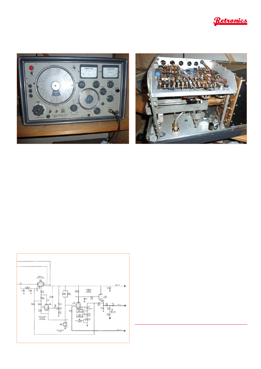
77
elektor 10-2012
sidering both the oscillator and the RF power amplifier have an RF
power capability of the order of 100 mW.
The circuit itself consists of ten tubes, a couple of semiconductor
diodes and a single Germanium transistor (OC71), and is not terribly
exciting from today’s perspective. Sections of the circuit diagram
are reproduced here, due to their size they cannot be printed in full.
The power supply consists of a transformer, a 5R4GY full-wave recti-
fier tube and a voltage stabiliser comprising a 5651 reference tube,
an EF95 (6AK5W) control amp and a KT66 audio output tube as the
regulating element. The filament voltage for the oscillator tube is
stabilised with a transductor (current-controlled inductance).
The RF signal is generated ‘straight off’, i.e. the oscillator oscillates
at the desired frequency (= sig gen output frequency) and its output
signal is buffered by an RF tetrode. The oscillator employs a TD03-
100 UHF triode with five switchable coils around it for the frequency
ranges. It is tuned with a variable capacitor. Unusually a heat sink is
found attached to the anode terminal of the triode.
The oscillator signal directly drives the symmetrical push-pull out-
put stage built around a QQV02-6 UHF dual tetrode. The tube oper-
ates in class A, resulting in maximum gain and low distortion (hence,
low harmonics). The DC level at the control grids allows the gain to
be controlled, or amplitude modulated if required. Thanks to the
gain control, the output voltage is independent of load as well as
frequency, making the measuring and matching of filters very con-
venient indeed.
The anode circuit of the amplifier also comprises five switchable
coils. Together with a second variable capacitor, the coils act as
tuneable resonant circuits tuned in synchronism with the oscillator.
To prevent tracking errors, the variable capacitor of the output cir-
cuit can be slightly detuned with respect to the oscillator — mechan-
ically, a not so simple design. The linear amplification afforded by
the push-pull output stage keeps harmonics generation down to a
minimum. The output signal is inductively coupled out through the
attenuator having a single calibrated range of 135 dB, and providing
a resistor network for a frequency-independent, rock steady output
impedance of 50 ohms.
The 5-position frequency range selection switch is also worth men-
tioning. Remarkably, the switch does not work as expected from
one marker to the next (to get to the next frequency range), but
requires an additional full turn. The switch itself is contactless, the
connection with the coils being capacitive. This has the advantage
of avoiding contact problems, which is highly relevant in view of the
tuned circuits’ Q (quality) factors.
Besides the everyday use of the instrument, the manual describes
maintenance and common repair steps in great detail, both
mechanical (like Bowden cable replacement) and electrical. I espe-
cially liked one tip for faultfinding: “Initially, look for burnt resistors
to locate a faulty circuit section”.
(120169)
Retronics is a monthly section in Elektor magazine covering
vintage electronics including legendary Elektor projects.
Contributions, suggestions and requests are welcomed; please send an
email to Jan Buiting (editor@elektor.com).
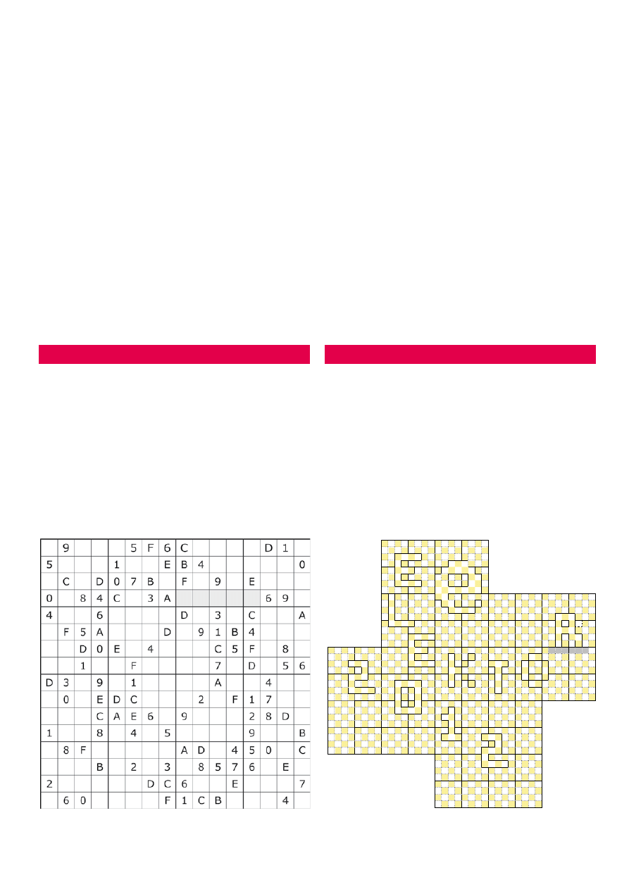
78
10-2012 elektor
INFOTAINMENT
Hexadoku
Puzzle with an electronics touch
Past page 75 or thereabouts and fed up with all that designing, programming and soldering? Then take a
break deservedly and give this puzzle a go. Enter the right numbers or letters A-F in the open boxes, find
the solution in the grey boxes, send it to us and you automatically enter the prize draw for one of four
Elektor Shop vouchers.
The instructions for this puzzle are straightforward. Fully geared to
electronics fans and programmers, the Hexadoku puzzle employs
the hexadecimal range 0 through F. In the diagram composed of
16 × 16 boxes, enter numbers such that all hexadecimal numbers
0 through F (that’s 0-9 and A-F) occur once only in each row, once
in each column and in each of the 4×4 boxes (marked by the thicker
black lines). A number of clues are given in the puzzle and these
determine the start situation. Correct entries received enter a draw
for a main prize and three lesser prizes. All you need to do is send us
the numbers in the grey boxes.
Solve Hexadoku and win!
Correct solutions received from the entire Elektor readership automati-
cally enter a prize draw for one Elektor Shop voucher worth £80.00 and
three Elektor Shop Vouchers worth £40.00 each, which should encour-
age all Elektor readers to participate.
Participate!
Before November 1, 2012,
send your solution (the numbers in the grey boxes) by email to:
hexadoku@elektor.com
Prize winners
The solution of the July & August 2012 Penta-Hexadoku is: D89276.
The Elektor £80.00 voucher has been awarded to Norbert Breuker (Germany).
The Elektor £40.00 vouchers have been awarded to Donald Hoogendorp (Netherlands),
Jean-Marie Bellet (France), and Mike Parker (United Kingdom).
Congratulations everyone!
The competition is not open to employees of Elektor International Media, its business partners and/or associated publishing houses.
C F 4 9 E 7 0 D 6 3 A B 2 1 8 5
B E 5 A 3 C F 2 1 4 D 8 9 0 7 6
0 1 6 7 A B 8 9 2 5 E F C 3 4 D
D 2 3 8 1 4 5 6 7 C 9 0 F E B A
E B 0 1 8 9 2 5 4 D C 3 A F 6 7
3 A F 4 B E 7 0 9 8 1 6 5 C D 2
2 7 C D 6 1 4 F A B 0 5 8 9 E 3
5 8 9 6 D A 3 C F E 7 2 B 4 1 0
A 5 8 3 2 F 6 7 E 1 4 9 0 D C B 4 9 0 1 8 5 6 7 2 B A 3 E F C D
7 0 D C 9 8 1 4 B 6 5 A 3 2 F E D 2 5 E F A 3 C 1 8 9 6 B 0 7 4
4 9 2 B C D E 3 0 F 8 7 6 5 A 1 6 B C 7 0 1 2 9 4 F E D 8 5 A 3
F 6 1 E 5 0 B A D 2 3 C 7 8 9 4 F 8 3 A B E D 4 7 0 5 C 1 2 9 6
6 D A 5 4 3 C B 8 9 2 1 E 7 0 F A 5 6 D 4 9 8 F E 3 0 7 C B 2 1
9 4 7 2 F 6 D 8 5 0 B E 1 A 3 C 9 4 7 2 1 0 B E 5 C F 8 3 6 D A
8 3 E F 0 5 A 1 C 7 6 D 4 B 2 9 E F 8 3 A D C 5 6 1 2 B 4 9 0 7
1 C B 0 7 2 9 E 3 A F 4 D 6 5 8 1 0 B C 3 2 7 6 9 A D 4 5 8 F E
8 D 4 3 E 9 C 1 2 F 0 B A 7 6 5 2 B 8 9 0 D E 3 C 1 4 F E B A 3 0 D 8 9 2 7 6 5
9 6 7 A B 8 5 0 1 4 D E 3 C F 2 1 4 5 A B 8 9 6 7 E D 0 5 C 9 2 3 6 1 A F 4 B 8
0 B C F A 7 2 D 6 5 8 3 E 1 4 9 6 D 0 7 C F A 5 8 3 2 B 6 F 0 D C 7 4 5 A 1 E 9
5 2 1 E 3 6 F 4 9 A 7 C D 8 B 0 F E 3 C 7 4 1 2 5 A 9 6 7 4 1 8 F 2 B E D C 3 0
6 9 0 7 4 1 A 3 E B C 5 2 D 8 F E 1 C 3 6 9 4 B 0 7 A 5 2 3 E B 8 9 C 1 6 D 4 F
3 A D 4 F 0 B 6 7 8 1 2 9 E 5 C 7 8 D 0 3 2 F A B 6 1 4 9 8 F 0 D E 3 2 7 A 5 C
C 5 2 1 8 D E 7 4 9 A F 6 B 0 3 A F 4 5 8 1 C 7 2 D E 9 C 7 4 1 A 5 6 F 0 3 8 B
F E B 8 5 C 9 2 D 6 3 0 1 A 7 4 B 6 9 2 5 0 D E 3 C F 8 D 6 5 A B 4 7 0 9 E 1 2
E 3 8 B 0 F 4 5 A 1 6 D C 9 2 7 4 5 E F A 3 8 D 6 B 0 1 2 9 C 7
7 0 F 6 9 2 D E 3 C B 8 5 4 1 A 9 2 7 6 F C B 0 D 8 3 E 1 A 5 4
4 1 A 5 C 3 6 B 0 7 2 9 8 F E D 0 3 A B 2 5 6 1 4 9 C 7 E F 8 D
D C 9 2 7 A 1 8 F E 5 4 B 0 3 6 D C 1 8 9 E 7 4 F 2 5 A B 6 3 0
A F 6 D 2 B 0 9 8 3 E 7 4 5 C 1 8 B 0 9 C D 2 F A 7 E 5 6 1 4 3
B 4 3 0 1 E 7 C 5 2 9 A F 6 D 8 F E 3 4 1 A 5 8 B C 9 6 D 0 7 2
2 7 E 9 6 5 8 F C D 4 1 0 3 A B C D 6 1 0 7 4 9 2 3 8 F A 5 E B
1 8 5 C D 4 3 A B 0 F 6 7 2 9 E 7 A 5 2 B 6 3 E 1 0 D 4 F C 9 8
A 9 4 5 8 B E 7 C F 6 D 0 3 2 1
3 6 F 0 D 2 1 A 9 E 7 8 5 4 B C
E 1 2 7 4 F C 3 0 5 A B 8 D 6 9
B 8 D C 5 0 9 6 3 4 1 2 7 E F A
2 F 8 D 6 9 0 B E 1 4 3 C 7 A 5
1 0 9 A 7 4 F 2 5 6 B C 3 8 D E
6 7 C 3 E 1 A 5 8 D 2 9 4 B 0 F
5 4 B E 3 8 D C 7 A F 0 9 2 1 6

2 29

ELEKTOR STORE
80
10-2012 elektor
More than 75,000 components
CD Elektor’s
Components Database 7
This CD-ROM gives you easy access to design data
for over 11,100 ICs, 37,000 transistors, FETs, thy-
ristors and triacs, 25,100 diodes and 2,000 opto-
couplers. The program package consists of eight
databanks covering ICs, transistors, diodes and op-
tocouplers. A further eleven applications cover the
calculation of, for example, zener diode series resis-
tors, voltage regulators, voltage dividers and AMV’s.
A colour band decoder is included for determining
resistor and inductor values. All databank applica-
tions are fully interactive, allowing the user to add,
edit and complete component data.
ISBN 978-90-5381-298-3 • £24.90 • US $40.20
A whole year of Elektor magazine
onto a single disk
DVD Elektor 2011
The year volume DVD/CD-ROMs are among the most
popular items in Elektor’s product range. This DVD-ROM
contains all editorial articles published in Volume 2011
of the English, American, Spanish, Dutch, French and
German editions of Elektor. Using the supplied Adobe
Reader program, articles are presented in the same lay-
out as originally found in the magazine. An extensive
search machine is available to locate keywords in any
article. With this DVD you can also produce hard copy
siasts will be keen to use Linux as the basis of a new
microcontroller project, but the apparent complexity
of the operating system and the high price of de-
velopment boards has been a hurdle. Here Elektor
solves both these problems, with a beginners’ course
accompanied by a compact and inexpensive popula-
ted and tested circuit board. This board includes eve-
rything necessary for a modern embedded project:
a USB interface, an SD card connection and various
other expansion options. It is also easy to hook the
board up to an Ethernet network.
Populated and tested Elektor Linux Board
Art.# 120026-91 • £57.80 • US $93.30
A comprehensive and practical
how-to guide
Design your own PC
Visual Processing
and Recognition
System in C#
This book is aimed at Engineers, Scientists and en-
thusiasts with developed programming skills or with
a strong interest in image processing technology on
a PC. Written using Microsoft C# and utilizing ob-
ject-oriented practices, this book is a comprehen-
sive and practical how-to guide. The key focus is on
modern image processing techniques with useful
of PCB layouts at printer resolution, and export circuit
diagrams and illustrations to other programs.
ISBN 978-90-5381-276-1 • £23.50 • US $37.90
LabWorX 2
Mastering Surface
Mount Technology
This book takes you on a crash course in techniques,
tips and know-how to successfully introduce sur-
face mount technology in your workfl ow. Even if you
are on a budget you too can jumpstart your designs
with advanced fi ne pitch parts. Besides explaining
methodology and equipment, attention is given to
SMT parts technologies and soldering methods. Many
practical tips and tricks are disclosed that bring sur-
face mount technology into everyone’s reach with-
out breaking the bank. A comprehensive kit of parts
comprising all SMT components, circuit boards and
solder stencils is available for readers wishing to rep-
licate three projects described in this book.
282 pages • ISBN 978-1-907920-12-7
£29.50 • US $47.60
Elektor Linux Board
Embedded Linux
Made Easy
Today Linux can be found running on all sorts of de-
vices, even coffee machines. Many electronics enthu-
Limited Time Offer for Elektor Magazine Members!
20% DISCOUNT
www.elektor.com/october
BOOKS, CD-ROM
S
, DVD
S
, KITS & MODULES
81
elektor 10-2012
and practical application examples to produce high-
quality image processing software. Analysis starts
with a detailed review of the fundamentals of im-
age processing. It progresses to explain and explore
the prac tical uses of two highly sophisticated and
freely downloadable, open source image processing
libraries; AForge.NET and Emgu.CV, utilizing dotnet
technology within the Microsoft Visual Studio envi-
ronment. All code examples used are available – free
of charge – from the Elektor website; you can easily
create and develop your own results to demonstrate
the concepts and techniques explained.
307 pages • ISBN 978-1-907920-09-7
£35.50 • US $57.30
Free Software CD-ROM included
Elementary Course
BASCOM-AVR
The Atmel AVR family of microcontrollers are ex-
tremely versatile and widely used. In Elektor maga-
zine we have already published many interesting
applications employing an ATmega or ATtiny micro-
controller. The majority of these projects perform a
particular function. In this book we focus more on the
software aspects. Using lots of practical examples we
show how, using BASCOM, you can quickly get your
own design ideas up and running in silicon.
224 pages • ISBN 978-1-907920-11-0
£34.95 • US $56.40
Ultrasensitive wideband E-smog detector
TAPIR Sniffs it Out!
Attention boy scouts, professionals and grandfathers!
This ultrasensitive wideband E-smog detector offers
you two extra senses to track down noise that’s nor-
mally inaudible. TAPIR — short for Totally Archaic
but Practical Interceptor of Radiation — also makes
a nice project to build: the kit comprises everything
you need. Even the enclosure, ingeniously consist-
ing of the PCB proper! Using the TAPIR is dead easy.
Connect the headphones and an antenna and switch
it on. Move it around any electrical device and you’ll
hear different noises with each device, depending on
the type and frequency of the emitted fi eld.
Kit of parts, incl. PCB
Art.# 120354-71 • £13.30 • US $21.50
Circuits, ideas, tips and tricks
CD 1001 Circuits
This CD-ROM contains more than 1000 circuits, ide-
as, tips and tricks from the Summer Circuits issues
2001-2010 of Elektor, supplemented with various
other small projects, including all circuit diagrams,
des criptions, component lists and full-sized layouts.
The articles are grouped alphabeti cally in nine dif-
ferent sections: audio & video, computer & micro-
controller, hobby & modelling, home & garden, high
frequency, power supply, robotics, test & measure-
ment and of course a section miscellaneous for eve-
rything that didn’t fi t in one of the other sections.
ISBN 978-1-907920-06-6 • £34.50 • US $55.70
Package Deal: 12% off
AVR Software
Defined Radio
This package consists of the three boards associated
with the AVR Software Defined Radio articles series in
Elektor, which is built around practical experiments.
The first board, which includes an ATtiny2313, a 20
MHz oscillator and an R-2R DAC, will be used to make
a signal generator. The second board will fi sh signals
out of the ether. It contains all the hardware needed
to make a digital software-defi ned radio (SDR), with
an RS-232 interface, an LCD panel, and a 20 MHz
VCXO (voltage-controlled crystal oscillator), which
can be locked to a reference signal. The third board
provides an active ferrite antenna.
Signal Generator + Universal Receiver +Active
Antenna: PCBs and all components + USB-FT232R
breakout-board
Art.# 100182-72 • £99.90 • US $133.00
Avoid interference and earth loops
USB Isolator
If your USB device ever suffers from noise caused
by an earth loop or if you want to protect your PC
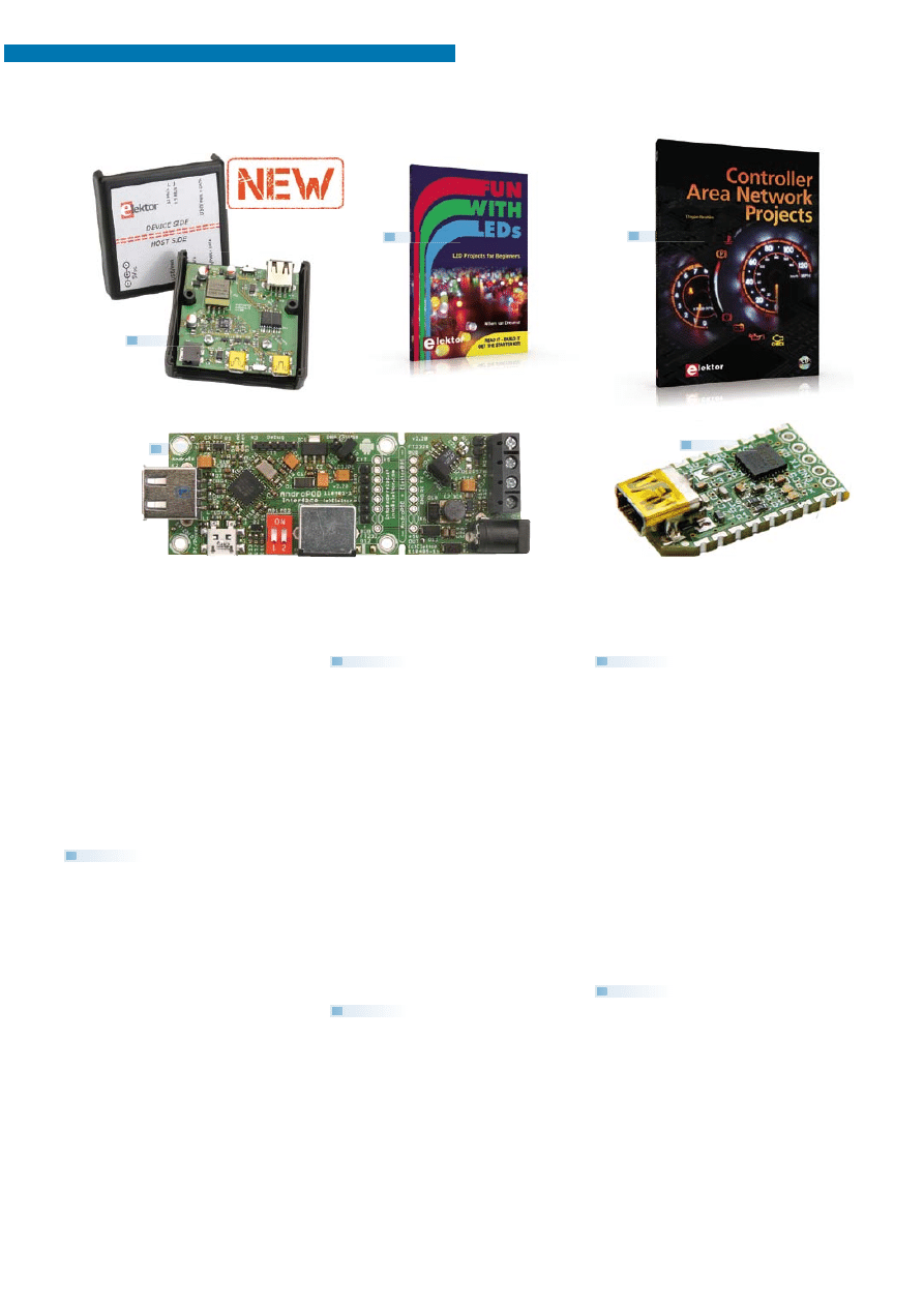
ELEKTOR STORE
82
10-2012 elektor
against external voltages then you need a USB iso-
lator. The circuit described in Elektor’s October 2012
edition offers an optimal electrical isolation of both
the data lines as well as the supply lines between the
PC and the USB device.
Populated and tested Board
Art.# 120291-91 • £62.30 • US $101.40
Associated 60-piece Starter Kit available
Fun with LEDs
This booklet presents more than twenty exciting
projects covering LEDs, aimed at young & old. From
an Air Writer, a Party Light, Running Lights, a LED
Fader right up to a Christmas Tree. Use this book to
replicate various projects and then put them into
practice. To give you a head start each project is
supported by a brief explanation, schematics and
photos. In addition, the free support page on the
Elektor website has a few inspiring video links avail-
able that elaborate on the projects. A couple of pro-
jects employ the popular Arduino microcontroller
board that’s graced by a galaxy of open source ap-
plications. The optional 60-piece Starter Kit avail-
able with this book is a great way to get circuits
built up and tested on a breadboard, i.e. without
soldering.
96 pages • ISBN 978-1-907920-05-9
£16.95 • US $38.00
Free mikroC compiler CD-ROM included
Controller Area
Network Projects
The aim of the book is to teach you the basic prin-
ciples of CAN networks and in addition the develop-
ment of microcontroller based projects using the
CAN bus. You will learn how to design microcontroller
based CAN bus nodes, build a CAN bus, develop high-
level programs, and then exchange data in real-time
over the bus. You will also learn how to build micro-
controller hardware and interface it to LEDs, LCDs,
and A/D converters.
260 pages • ISBN 978-1-907920-04-2
£29.50 • US $47.60
Bridging Android and your electronics projects
AndroPod
With their high-resolution touchscreens, ample com-
puting power, WLAN support and telephone func-
tions, Android smartphones and tablets are ideal for
use as control centres in your own projects. However,
up to now it has been rather diffi cult to connect them
to exter-nal circuitry. Our AndroPod interface board,
which adds a serial TTL port and an RS485 port to the
picture, changes this situation.
Andropod module w th RS485 Extension
Art.# 110405-91 • £53.35 • US $74.70
Meet BOB
FT232R USB/
Serial Bridge/BOB
You’ll be surprised fi rst and foremost by the size of this
USB/serial converter – no larger than the moulded plug
on a USB cable! And you’re also bound to appreciate
that fact that it’s practical, quick to implement, reus-
able, and multi-platform – and yet for all that, not too
expensive! Maybe you don’t think much of the various
commercially-available FT232R-based modules. Too ex-
pensive, too bulky, badly designed, That’s why this pro-
ject got designed in the form of a breakout board (BOB).
PCB, assembled and tested
Art.# 110553-91 • £12.90 • US $20.90
110 issues, more than 2,100 articles
DVD Elektor
1990 through 1999
This DVD-ROM contains the full range of 1990-1999
volumes (all 110 issues) of Elek tor Electronics maga-
zine (PDF). The more than 2,100 separate articles
have been classifi ed chronologically by their dates of
publication (month/year), but are also listed alpha-
betically by topic. A comprehensive index enables
you to search the entire DVD. What’s more, this DVD
also con tains the entire ‘The Elektor Datasheet Col-
lection 1...5’ CD-ROM series.
ISBN 978-0-905705-76-7 • £69.00 • US $111.30
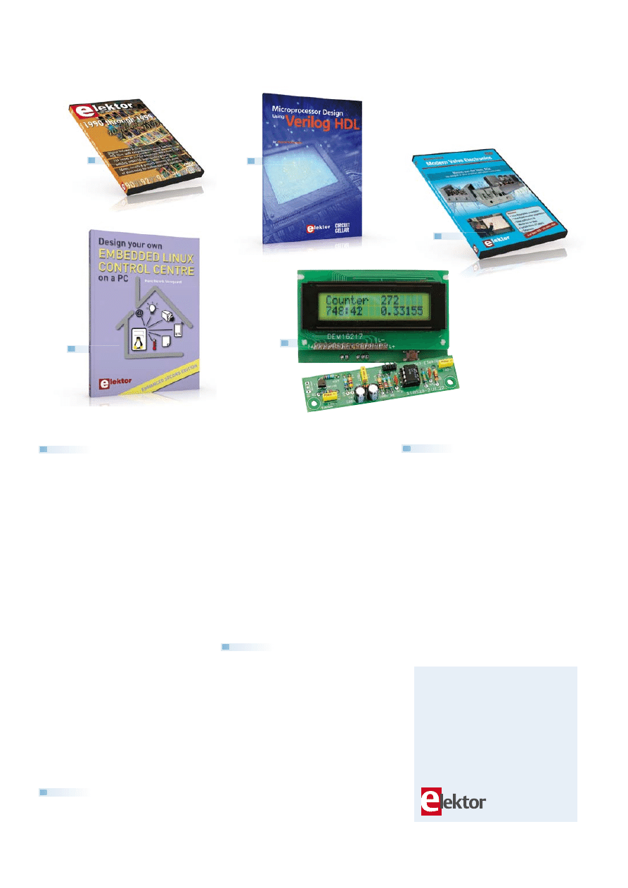
BOOKS, CD-ROM
S
, DVD
S
, KITS & MODULES
83
elektor 10-2012
Enhanced second edition
Design your own
Embedded Linux
Control Centre on a PC
The main system described in this book reuses an
old PC, a wireless mains outlet with three switches
and one controller, and a USB webcam. All this is
linked together by Linux. This book will serve up the
basics of setting up a Linux environment – including
a software development environment – so it can be
used as a control centre. The book will also guide
you through the necessary setup and confi guration
of a webserver. New edition enhancements include
details of extending the capabilities of your control
center with ports for a mobile phone (for SMS mes-
saging) and the Elektor “thermo snake” for lowcost
networked real-time thermal monitoring of your
house and outbuildings. Now you can additionally
also send all kinds of useful temperature and sensor
warnings to a mobile phone. All software needed will
be available at the Elektor website.
416 pages • ISBN 978-1-907920-02-8
£34.50 • US $55.70
Processor design in the real world
Microprocessor Design
using Verilog HDL
If you have the right tools, designing a microproces-
sor shouldn’t be complicated. The Verilog hardware
description language (HDL) is one such tool. This
book is a practical guide to processor design in the
real world. It presents the Verilog HDL in an easily digest-
ible fashion and serves as a thorough introduction about
reducing a computer architecture and instruction set
to practice. You’re led through the microprocessor de-
sign process from the start to fi nish, and essential topics
ranging from writing in Verilog to debugging and tes-
ting are laid bare.
340 pages • ISBN 978-0-9630133-5-4
£27.90 • US $45.00
Counter for alpha, beta and
gamma radiation
Improved
Radiation Meter
This device can be used with different sensors to meas-
ure gamma and alpha radiation. It is particularly suit-
able for long-term measurements and for examining
weakly radio-active samples. The photodiode has a
smaller sensitive area than a Geiger-Müller tube and so
has a lower background count rate, which in turn means
that the radiation from a small sample is easier to de-
tect against the background. A further advantage of a
semiconductor sensor is that is offers the possibility of
measuring the energy of each particle.
Kit of parts incl. display and programmed controller
Art.# 110538-71 • £35.50 • $57.30
Dual-layer DVD: 165 mins. video
DVD Modern Valve
Electronics
This fi lmed seminar (presented by Menno van der
Veen) starts with a short discussion of the classic ap-
proach using valve load line graphs, followed by cur-
rent sources and current foldback techniques. Next,
the negative effect of cathode electrolytics is covered
as well as reducing supply voltage interference. With
the help of state of the art measurement techniques
the (in)correctness of feedback is proven, while also
clarifying what’s happening deep within the core of
the output transformer.
ISBN 978-1-907920-10-3 • £24.90 • US $40.20
More information on the
Elektor Website:
www.elektor.com/store
Elektor
78 York Street
London - W1H 1DP
United Kingdom
Tel.: +44 20 7692 8344
Email: order@elektor.com
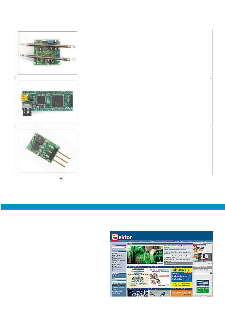
84
10-2012 e lektor
COMING ATTRACTIONS
next month in elektor
Article titles and magazine contents subject to change; please check the magazine tab on www.elektor.com
elektor Uk/european october 2012 edition on sale october 18, 2012. elektor USA october 2012 edition published october 15, 2012.
Elektor on the web
ww.elektor.com www.elektor.com www.elektor.com www.elektor.com www.elektor.com ww
All magazine articles back to volume 2000 are available individually in pdf format against e-credits. Article summaries and compo-
nent lists (if applicable) can be instantly viewed to help you positively identify an article. Article related items and resources are also
shown, including software downloads, hyperlinks, circuit boards, programmed ICs and corrections and updates if applicable.
In the Elektor Shop you’ll find all other products sold by the
publishers, like CD-ROMs, DVDs, kits, modules, equipment,
tools and books. A powerful search function allows you to
search for items and references across the entire website.
Also on the Elektor website:
•
Electronics news and Elektor announcements
•
Readers Forum
•
PCB, software and e-magazine downloads
•
Time limited offers
•
FAQ, Author Guidelines and Contact
Cool! 7805 Drop-in
The 7805 is unquestionably the most widely used fixed voltage regulator. Unfortunately
this golden oldie has a habit of turning all the excess energy into heat. Wouldn’t it be nice
to have a switching power supply controller as a drop-in replacement for the 7805? The
switched device is sure to offer much higher efficiency as well as better specifications. In
the Elektor labs, a small printed circuit board was designed around a TPS62150 buck con-
verter capable of turning an input voltage of 5.5 to 17 V into a 5 V stabilized rail at up to 1 A.
By adjusting a number of resistance values, other output voltages are also possible.
(we are sorry this article could not be published in the October 2012 edition as planned)
Nixie VU Meter
After various Nixie clocks, thermometers and a hygrometer, a Nixie VU meter gets
described in Elektor next month. This circuit is designed to embellish a (tube) amplifier. It
supplies beautiful light effects but it is not calibrated to represent instantaneous output
power in any exact way. At the heart of the circuit is a Cypress PSoC type CY8C27443,
which determines the level of two audio channels and looks after the driving of two Rus-
sian Nixie tubes type IN-9.
Elektor FPGA Board
Always wanted to start working with FPGAs, but found nothing but hindrances in your
way? Elektor now has a great option for you: an affordable FPGA developer’s board that’s
easy to use, as well as to extend by way of a standard breadboard. The microcontroller on
the board takes care of the communicating with the PC via USB, while the configuration
data for the FPGA are stored on a micro-SD card located on the board too. Using Windows
a configuration file can easily be transferred on to the SD card; when the card is reset this
configuration file gets written into the FPGA.

85
elektor 10-2012
ORDERING INSTRUCTIONS, P&P CHARGES
Non-online orders, except for memberships (for which see below), must be sent BY POST or FAX to
Elektor International Media, 78 York Street, London W1H 1DP, United Kingdom.
Online ordering: www.elektor.com/store
Orders placed on our London office must include P&P charges (Priority or Standard) as follows:
Europe: £6.00 (Standard) or £7.00 (Priority). Outside Europe: £9.00 (Standard) or £11.00 (Priority)
HOW TO PAY
All orders must be accompanied by the full payment, including postage and packing charges as stated above or advised by Customer Services staff.
Bank transfer into account no. 40270211 held by Elektor International Media BV with The Royal Bank of Scotland, London.
IBAN: GB96 ABNA 4050 3040 2702 11. BIC: ABNAGB2L. Currency: sterling (UKP).
Please ensure your full name and address gets communicated to us.
Cheque sent by post, made payable to Elektor Electronics. We can only accept sterling cheques and bank drafts from UK-resident customers or members.
We regret that no cheques can be accepted from customers or members in any other country.
Credit card VISA and MasterCard can be processed by mail, email, web, fax and telephone. Online ordering through our website is SSL-protected for your
security.
COMPONENTS
If difficulties are envisaged in the supply of components for Elektor projects, a source will normally be advised in the article.
Note, however, that the source(s) given is (are) not exclusive.
TERMS OF BUSINESS
Delivery Although every effort will be made to dispatch your order within 2-3 weeks from receipt of your instructions, we can not guarantee this time
scale for all orders.
Returns Faulty goods or goods sent in error may be returned for replacement or refund, but not before obtaining our consent. All goods returned should
be packed securely in a padded bag or box, enclosing a covering letter stating the dispatch note number. If the goods are returned because of a mistake on
our part, we will refund the return postage.
Damaged goods Claims for damaged goods must be received at our London office within 10 days (UK); 14 days (Europe) or 21 days (all other countries).
Cancelled orders All cancelled orders will be subject to a 10% handling charge with a minimum charge of £5.00.
Patents Patent protection may exist in respect of circuits, devices, components, and so on, described in our books and magazines. Elektor does not accept
responsibility or liability for failing to identify such patent or other protection.
Copyright All drawings, photographs, articles, printed circuit boards, programmed integrated circuits, diskettes and software carriers published in
our books and magazines (other than in third-party adverti-sements) are copyright and may not be reproduced or transmitted in any form or by any
means, including photocopying and recording, in whole or in part, without the prior permission of Elektor in writing. Such written permission must also
be obtained before any part of these publications is stored in a retrieval system of any nature. Notwithstanding the above, printed circuit boards may be
produced for private and personal use without prior permission.
Limitation of liability Elektor shall not be liable in contract, tort, or otherwise, for any loss or damage suffered by the purchaser whatsoever or howsoever
arising out of, or in connexion with, the supply of goods or services by Elektor other than to supply goods as described or, at the option of Elektor, to refund
the purchaser any money paid in respect of the goods.
Law Any question relating to the supply of goods and services by Elektor shall be determined in all respects by the laws of England.
MEMBERSHIP RATES FOR ANNUAL MEMBERSHIP
Standard
Plus
United Kingdom & Ireland
£54.00
£66.50
Surface Mail Rest of the World
£68.50
£81.00
Airmail Rest of the World
£86.00
£98.50
USA & Canada
See www.elektor.com/usa for special offers
HOW TO PAY
Bank transfer into account no. 40270211 held by Elektor International
Media BV with The Royal Bank of Scotland, London.
IBAN: GB96 ABNA 4050 3040 2702 11. BIC: ABNAGB2L.
Currency: sterling (UKP). Please ensure your full name and address gets
communicated to us.
Cheque sent by post, made payable to Elektor Electronics. We can only
accept sterling cheques and bank drafts from UK-resident customers or
members. We regret that no cheques can be accepted from customers or
members in any other country.
Credit card VISA and MasterCard can be processed by mail, email, web,
fax and telephone. Online ordering through www.elektor.com/store is SSL-
protected for your security.
MEMBERSHIP CONDITIONS
The standard membership order period is twelve months. If a permanent
change of address during the membership period means that copies have
to be despatched by a more expensive service, no extra charge will be
made. Conversely, no refund will be made, nor expiry date extended, if a
change of address allows the use of a cheaper service.
Student applications, which qualify for a 20% (twenty per cent)
reduction in current rates, must be supported by evidence of
studentship signed by the head of the college, school or university
faculty. A standard Student Membership costs £43.20, a Student Plus
Membership costs £55.70 (UK only).
Please note that new memberships take about four weeks from receipt of
order to become effective.
Cancelled memberships will be subject to a charge of 25% (twenty-five per
cent) of the full membership price or £7.50, whichever is the higher, plus
the cost of any issues already dispatched.
Memberships cannot be cancelled after they have run for six months or
more.
August 2012
52429

www.elektor-projects.com
Sharing Electronics Projects
Get elektorized too! Check www.elektor-projects.com
Get Elektorized
Elektor Projects is an online community
for people passionate about electronics.
Here you can share your projects and
participate in those created by others.
It’s a place where you can discuss project
development and electronics.
Elektor’s team of editors and engineers
assist you to bring your projects to a
good end. They can help you write an
article to be published in Elektor maga-
zine or even develop a complete product
that you can sell in the Elektor Shop!
JOIN
NOW!
2 29
$25
Print or Digital ::
$50
Combo
Celebrate Circuit Cellar’s 25th year
of bringing
readers insightful analysis of embedded electronics technology.
Visit
www.circuitcellar.com/el912
to take advantage of these great deals.
Celebrate Circuit Cellar’s
25
th
Anniversary
Sign up today and you’ll also receive the
Special 25
th
Anniversary Edition
with your subscription!
SPECIAL:
SAVE 50%
SPECIAL:
SAVE 50%
SPECIAL
ONUS OFFER! BONUS OFFER! BONUS OFFER! BONUS OFF
2 29

PROTEUS DESIGN SUITE
Features:
Our completely new manual router makes placing tracks quick and intuitive. During track
placement the route will follow the mouse wherever possible and will intelligently move
around obstacles while obeying the design rules.
All versions of Proteus also include an integrated world class shape based auto-router as
standard.
<
Board Autoplacement & Gateswap Optimiser.
<
Direct CADCAM, ODB++, IDF & PDF Output.
<
Integrated 3D Viewer with 3DS and DXF export.
<
Mixed Mode SPICE Simulation Engine.
<
Co-Simulation of PIC, AVR, 8051 and ARM7.
<
Direct Technical Support at no additional cost.
<
<
<
<
<
<
Hardware Accelerated Performance.
Unique Thru-View™ Board Transparency.
Over 35k Schematic & PCB library parts.
Integrated Shape Based Auto-router.
Flexible Design Rule Management.
Polygonal and Split Power Plane Support.
Labcenter Electronics Ltd. 53-55 Main Street, Grassington, North Yorks. BD23 5AA.
Registered in England 4692454 Tel: +44 (0)1756 753440, Email: info@labcenter.com
Visit our website or
phone 01756 753440
for more details
Prices start from just £150 exc. VAT & delivery
ROUTE FASTER !
WITH PROTEUS PCB DESIGN
2 29
Wyszukiwarka
Podobne podstrony:
Elektor Electronics October 2012
Elektor Electronics UK November 2012 (True PDF)
Elektor Electronics UK May 2012
Elektor Electronics UK November 2012 (True PDF)
Elektor Electronics No 10 10 2011
Elektor Electronics 2005 07 08
PL PRINCE2 Foundation Sample Paper 1 October 2012 Polish
Elektor Electronics 2007 05
Elektor Electronics 2007 09
PL PRINCE2 Foundation Sample Paper 1 Rationale October 2012 Polish
Elektor Electronics 2007 06
Elektor Electronics 2007 01
PL PRINCE2 Foundation Sample Paper 1 Answer Key October 2012 Polish
Elektor Electronics 2005 03
Elektor Electronics No 10 10 2011
Elektor Electronics 2007 06
James Wood reviews Portrait of a Novel by Michael Gorra LRB 11
więcej podobnych podstron