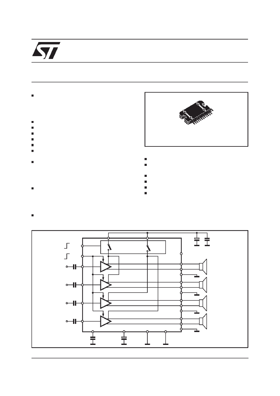
TDA7385
4 x 30W QUAD BRIDGE CAR RADIO AMPLIFIER
HIGH OUTPUT POWER CAPABILITY:
4 x 35W/4
Ω
MAX.
4 x 30W/4
Ω
EIAJ
4 x 22W/4
Ω
@ 14.4V, 1KHz, 10%
4 x 18.5W/4
Ω
@ 13.2V, 1KHz, 10%
CLIPPING DETECTOR
LOW DISTORTION
LOW OUTPUT NOISE
ST-BY FUNCTION
MUTE FUNCTION
AUTOMUTE AT MIN. SUPPLY VOLTAGE DE-
TECTION
DIAGNOSTICS FACILITY FOR:
– CLIPPING
– OUT TO GND SHORT
– OUT TO V
S
SHORT
– THERMAL SHUTDOWN
LOW EXTERNAL COMPONENT COUNT:
– INTERNALLY FIXED GAIN (26dB)
– NO EXTERNAL COMPENSATION
– NO BOOTSTRAP CAPACITORS
PROTECTIONS:
OUTPUT SHORT CIRCUIT TO GND, TO V
S
,
ACROSS THE LOAD
VERY INDUCTIVE LOADS
OVERRATING CHIP TEMPERATURE WITH
SOFT THERMAL LIMITER
LOAD DUMP VOLTAGE
FORTUITOUS OPEN GND
REVERSED BATTERY
ESD PROTECTION
DESCRIPTION
The TDA7385 is a new technology class AB
Audio Power Amplifier in Flexiwatt 25 package
March 2001
ORDERING NUMBER: TDA7385
IN1
0.1
µ
F
MUTE
ST-BY
IN2
0.1
µ
F
OUT1+
OUT1-
OUT2+
OUT2-
PW-GND
IN3
0.1
µ
F
IN4
0.1
µ
F
OUT3+
OUT3-
OUT4+
OUT4-
PW-GND
PW-GND
PW-GND
D93AU002C
AC-GND
0.1
µ
F
47
µ
F
SVR
TAB
S-GND
Vcc1
Vcc2
100nF
2.200
µ
F
DIAGN. OUT
BLOCK AND APPLICATION DIAGRAM
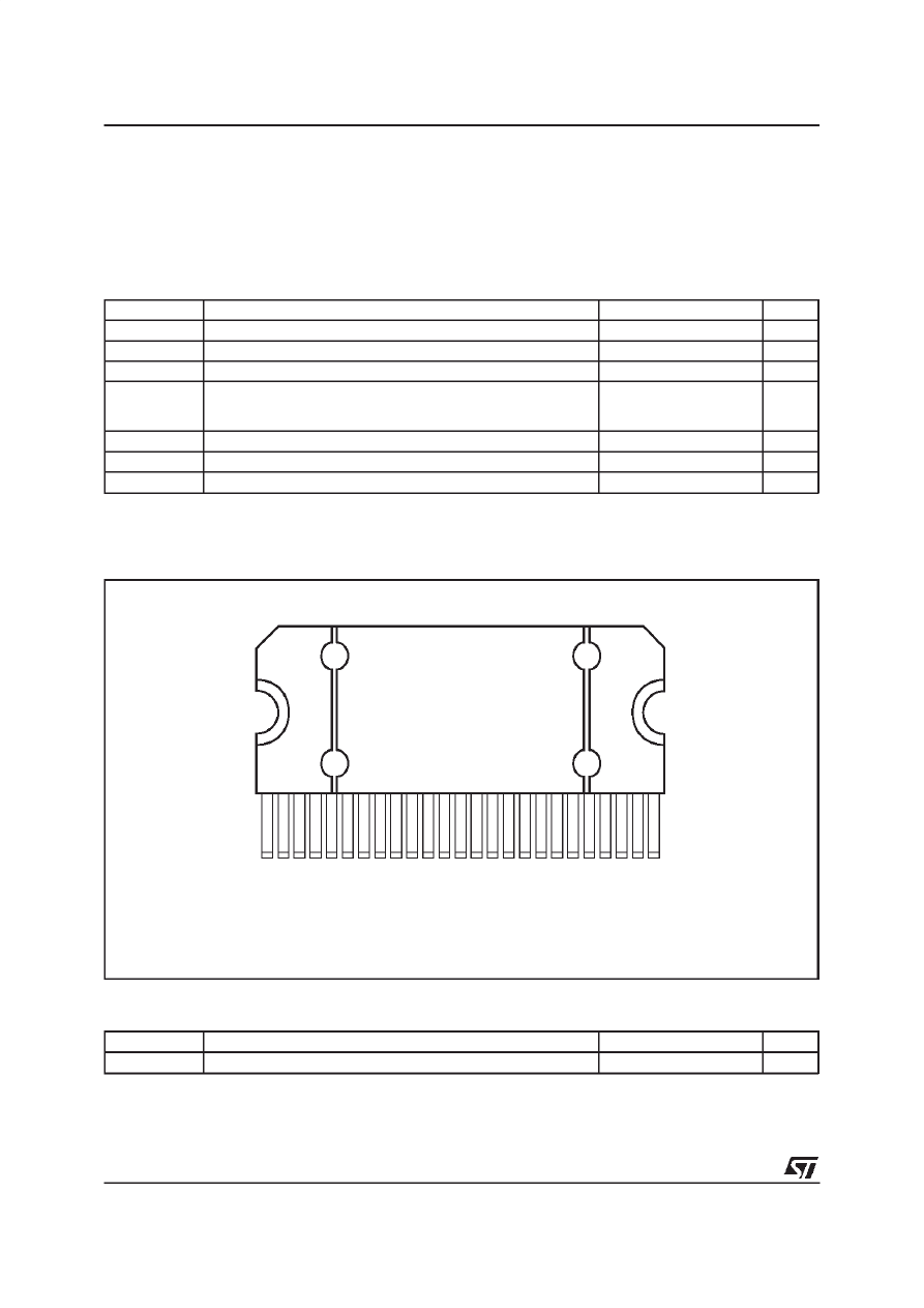
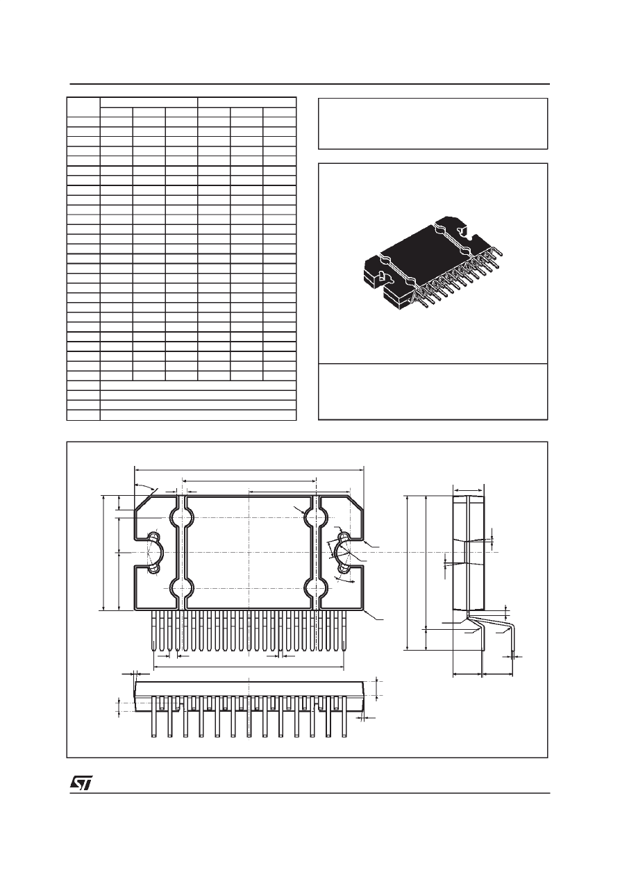
FLEXIWATT25
1/12
designed for high end car radio applications.
D94AU117B
TAB
P-GND
OUT2-
ST-BY
OUT2+
V
CC
OUT1-
P-GND1
OUT1+
SVR
IN1
IN2
S-GND
IN4
IN3
AC-GND
OUT3+
P-GND3
OUT3-
V
CC
OUT4+
MUTE
OUT4-
P-GND4
DIAGNOSTICS
1
25
PIN CONNECTION (Top view)
ABSOLUTE MAXIMUM RATINGS
Symbol
Parameter
Value
Unit
V
CC
Operating Supply Voltage
18
V
V
CC (DC)
DC Supply Voltage
28
V
V
CC (pk)
Peak Supply Voltage (t = 50ms)
50
V
I
O
Output Peak Current:
Repetitive (Duty Cycle 10% at f = 10Hz)
Non Repetitive (t = 100
µ
s)
4.5
5.5
A
A
P
tot
Power dissipation, (T
case
= 70
°
C)
80
W
T
j
Junction Temperature
150
°
C
T
stg
Storage Temperature
– 55 to 150
°
C
THERMAL DATA
Symbol
Parameter
Value
Unit
R
th j-case
Thermal Resistance Junction to Case
Max.
1
°
C/W
Thanks to the fully complementary PNP/NPN out-
put configuration the TDA7385 allows a rail to rail
output voltage swing with no need of bootstrap
capacitors. The extremely reduced components
count allows very compact sets.
The on-board clipping detector simplifies gain
compression operations. The fault diagnostics
makes it possible to detect mistakes during Car-
Radio assembly and wiring in the car.
DESCRIPTION (continued)
TDA7385
2/12
ELECTRICAL CHARACTERISTICS (V
S
= 14.4V; f = 1KHz; R
g
= 600
Ω
; R
L
= 4
Ω
; T
amb
= 25
°
C;
Refer to the Test and application circuit (fig.1), unless otherwise specified.)
Symbol
Parameter
Test Condition
Min.
Typ.
Max.
Unit
I
q1
Quiescent Current
180
300
mA
V
OS
Output Offset Voltage
100
mV
G
v
Voltage Gain
25
26
27
dB
P
o
Output Power
THD = 10%
THD = 1%
THD = 10%; V
S
= 14V
THD = 5%; V
S
= 14V
THD = 1%; V
S
= 14V
THD = 10%; V
S
= 13.2V
THD = 1%; V
S
= 13.2V
20
16.5
19
17
16
17
14
22
18
21
19
17
18.5
15
W
W
W
W
W
W
W
P
o EIAJ
EIAJ Output Power (*)
VS = 13.7V
27.5
30
W
P
o max.
Max. Output Power (*)
V
S
= 14.4V
33
35
W
THD
Distortion
P
o
= 4W
0.04
0.3
%
e
No
Output Noise
”A” Weighted
Bw = 20Hz to 20KHz
50
65
150
µ
V
µ
V
SVR
Supply Voltage Rejection
f = 100Hz
50
65
dB
f
cl
Low Cut-Off Frequency
20
Hz
f
ch
High Cut-Off Frequency
75
KHz
R
i
Input Impedance
70
100
K
Ω
C
T
Cross Talk
f = 1KHz
50
70
dB
I
SB
St-By Current Consumption
St-By = LOW
50
µ
A
V
SB out
St-By OUT Threshold Voltage
(Amp: ON)
3.5
V
V
SB IN
St-By IN Threshold Voltage
(Amp: OFF)
1.5
V
A
M
Mute Attenuation
V
O
= 1Vrms
80
90
dB
V
M out
Mute OUT Threshold Voltage
(Amp: Play)
3.5
V
V
M in
Mute IN Threshold Voltage
(Amp: Mute)
1.5
V
I
m (L)
Muting Pin Current
V
MUTE
= 1.5V
(Source Current)
5
10
16
µ
A
I
CDOFF
Clipping Detector ”OFF” Output
Average Current
THD = 1% (**)
100
µ
A
I
CDON
Clipping Detector ”ON” Output
Average Current
THD = 10% (**)
100
240
350
µ
A
(*) Saturated square wave output.
(**) Diagnostics output pulled-up to 5V with 10K
Ω
series resistor.
TDA7385
3/12
IN1
0.1
µ
F
C9
1
µ
F
IN2
C2 0.1
µ
F
OUT1
OUT2
IN3
C3 0.1
µ
F
IN4
C4 0.1
µ
F
OUT3
OUT4
D94AU179B
C5
0.1
µ
F
C6
47
µ
F
SVR
TAB
Vcc1-2
Vcc3-4
C8
0.1
µ
F
C7
2200
µ
F
C10
1
µ
F
ST-BY
R1
10K
R2
47K
MUTE
C1
14
15
12
11
22
4
13
S-GND
16
10
25
1
DIAGNOSTICS
6
20
9
8
7
5
2
3
17
18
19
21
24
23
Figure 1: Standard Test and Application Circuit
TDA7385
4/12
TDA7385
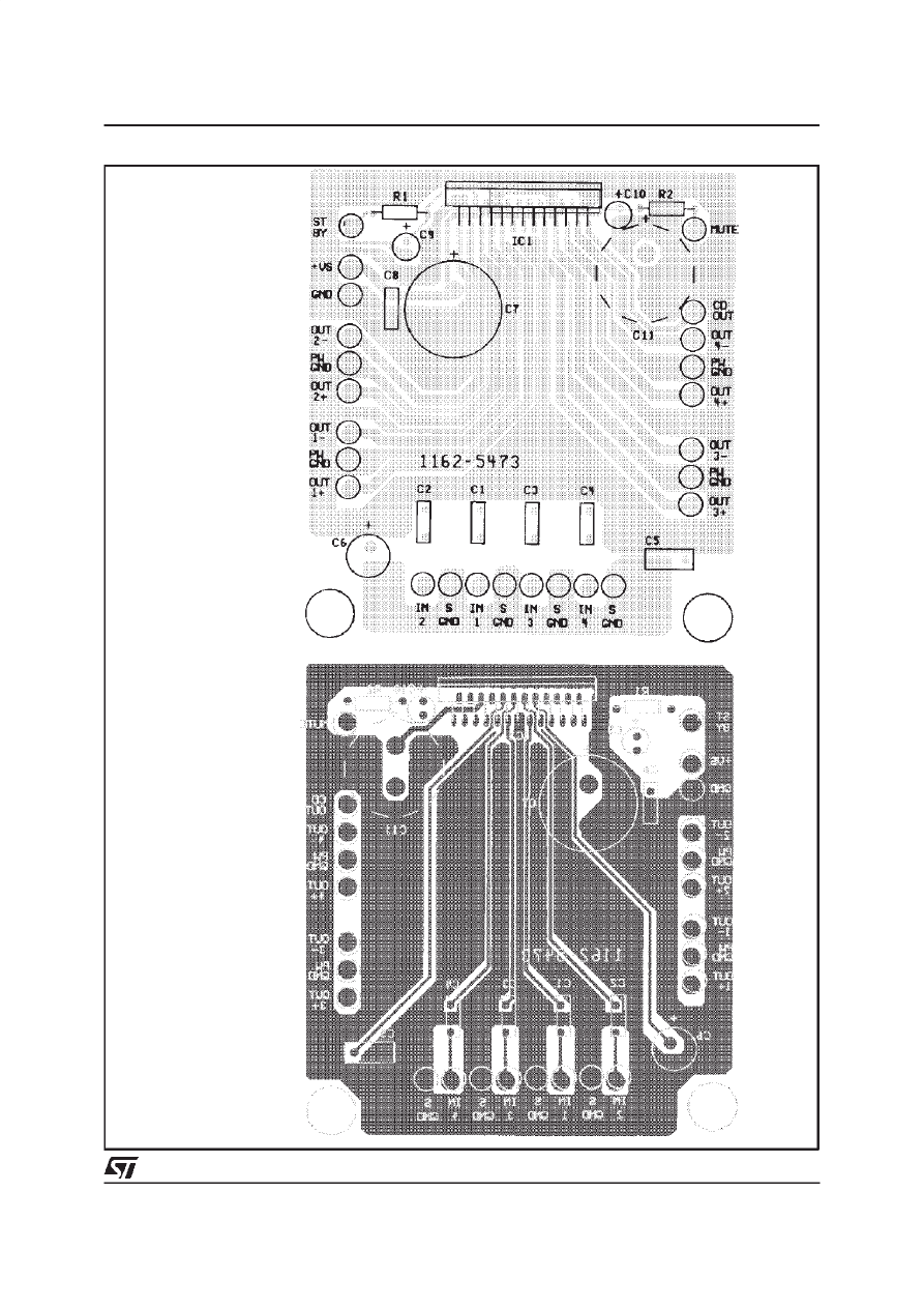
Figure 2: P.C.B. and component layout of the figure 1 (1:1 scale)
COMPONENTS &
TOP COPPER LAYER
BOTTOM COPPER LAYER
TDA7385
5/12
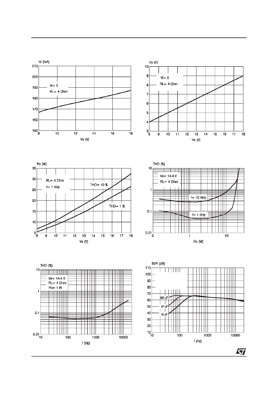
Figure 3: Quiescent Current vs. Supply Voltage
Figure 4: Quiescent Output Voltage vs. Supply
Voltage
Figure 5: Output Power vs. Supply Voltage
Figure 6: Distortion vs. Output Power
Figure 7: Distortion vs. Frequency.
Figure 8: Supply
Voltage
Rejection
vs.
Frequency by varying C6
R
g
= 600
Ω
V
ripple
= 1Vrms
TDA7385
6/12
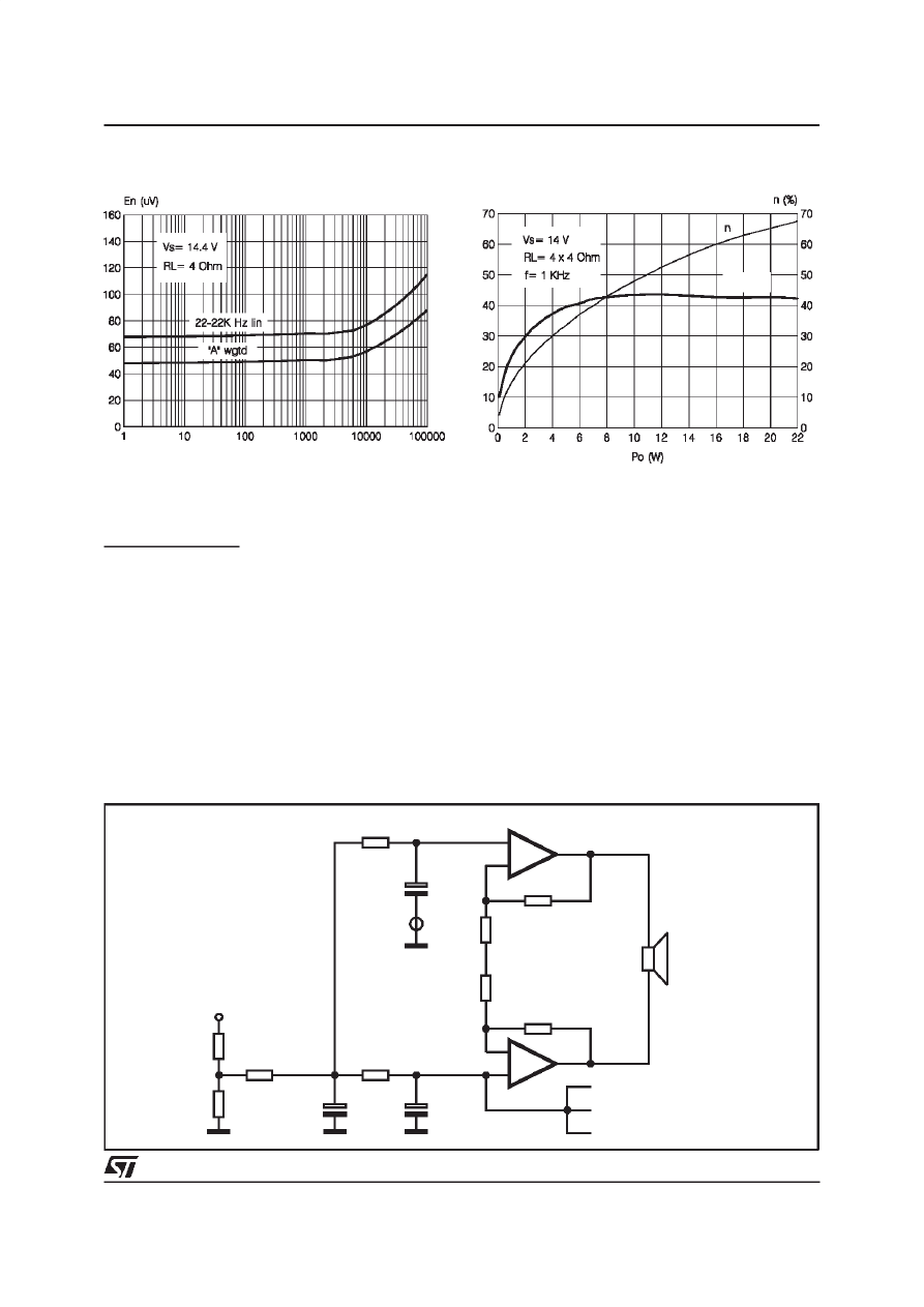
Figure 9: Output Noise vs. Source Resistance
Figure 10: Power Dissipation & Efficiency vs.
Output Power
R
g
(
Ω
)
P
to t
(W)
P
tot
APPLICATION HINTS (ref. to the circuit of fig. 1)
BIASING AND SVR
As shown by fig. 11, all the TDA7385’s main sec-
tions, such as INPUTS, OUTPUTS AND AC-GND
(pin 16) are internally biased at half Supply Volt-
age level (Vs/2), which is derived from the Supply
Voltage Rejection (SVR) block. In this way no cur-
rent flows through the internal feedback network.
The AC-GND is common to all the 4 amplifiers
and represents the connection point of all the in-
verting inputs.
Both individual inputs and AC-GND are con-
nected to Vs/2 (SVR) by means of 100K
Ω
resis-
tors.
To ensure proper operation and high supply volt-
age rejection, it is of fundamental importance to
provide a good impedance matching between IN-
PUTS and AC-GROUND terminations. This im-
plies that C
1
, C
2
, C
3
, C
4
, C
5
CAPACITORS HAVE
TO CARRY THE SAME NOMINAL VALUE AND
THEIR TOLERANCE SHOULD NEVER EXCEED
±
10 %.
Besides its contribution to the ripple rejection, the
SVR capacitor governs the turn ON/OFF time se-
quence and, consequently, plays an essential role
in the pop optimization during ON/OFF transients.
To conveniently serve both needs, ITS MINIMUM
RECOMMENDED VALUE IS 10
µ
F.
+
-
0.1
µ
F
C1
÷
C4
+
-
8K
Ω
8K
Ω
400
Ω
400
Ω
100K
Ω
100K
Ω
70K
Ω
IN
D95AU302
TOWARDS
OTHER CHANNELS
10K
Ω
10K
Ω
V
S
47
µ
F
C6
0.1
µ
F
C5
SVR
AC_GND
Figure 11: Input/OutputBiasing.
TDA7385
7/12
INPUT STAGE
The TDA7385’S inputs are ground-compatible
and can stand very high input signals (
±
8Vpk)
without any performances degradation.
If the standard value for the input capacitors
(0.1
µ
F) is adopted, the low frequency cut-off will
amount to 16 Hz.
STAND-BY AND MUTING
STAND-BY and MUTING facilities are both
CMOS-COMPATIBLE. If unused, a straight con-
nection to Vs of their respective pins would be ad-
missible. Conventional low-power transistors can
be employed to drive muting and stand-by pins in
absence of true CMOS ports or microprocessors.
R-C cells have always to be used in order to
smooth down the transitions for preventing any
audible transient noises.
Since a DC current of about 10 uA normally flows
out of pin 22, the maximum allowable muting-se-
ries resistance (R
2
) is 70K
Ω
, which is sufficiently
high to permit a muting capacitor reasonably
small (about 1
µ
F).
If R
2
is higher than recommended, the involved
risk will be that the voltage at pin 22 may rise to
above the 1.5 V threshold voltage and the device
will consequently fail to turn OFF when the mute
line is brought down.
About the stand-by, the time constant to be as-
signed in order to obtain a virtually pop-free tran-
sition has to be slower than 2.5V/ms.
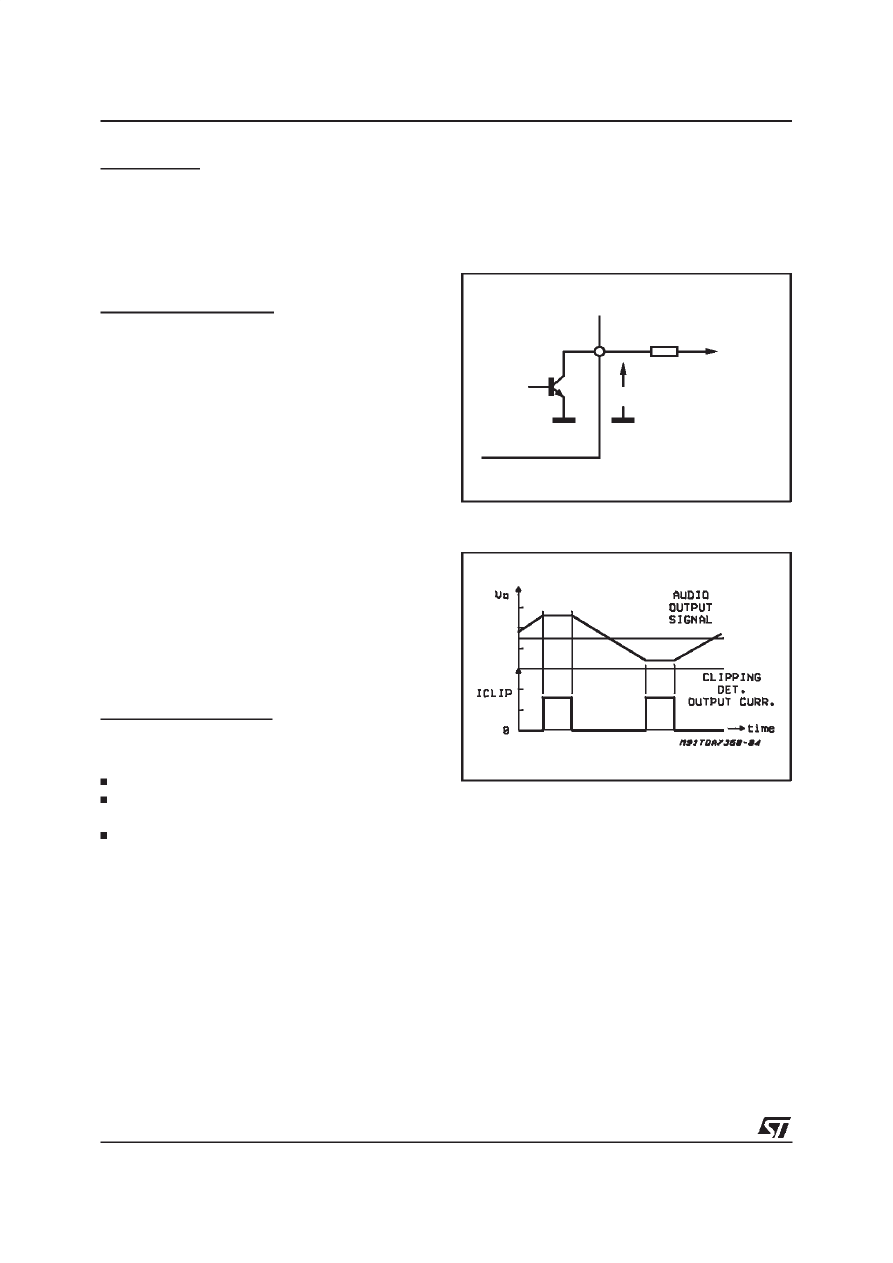
DIAGNOSTICS FACILITY
The TDA7385 is equipped with a diagnostics cir-
cuitry able to detect the following events:
CLIPPING in the output stage
OVERHEATING
(THERMAL
SHUT-DOWN
proximity)
OUTPUT MISCONNECTIONS (OUT-GND &
OUT-Vs shorts)
Diagnostics information is available across an
open collector output located at pin 25 (fig. 12)
through a current sinking whenever at least one
of the above events is recognized.
Among them, the CLIPPING DETECTOR acts in
a way to output a signal as soon as one or more
power transistors start being saturated.
As a result, the clipping-related signal at pin 25
takes the form of pulses, which are perfectly syn-
cronized with each single clipping event in the
music program and reflect the same duration time
(fig. 13).
Applications making use of this facility
usually operate a filtering/integration of the pulses
train through passive R-C networks and realize a
volume (or tone bass) stepping down in associa-
tion with microprocessor-driven audioprocessors.
The maximum load that pin 25 can sustain is
1K
Ω
.
Due to its operating principles, the clipping detec-
tor has to be viewed mainly as a power-depend-
ent feature rather than frequency-dependent.This
means that clipping state will be immediately sig-
naled out whenever a fixed power level is
reached, regardless of the audio frequency.
In other words, this feature offers the means to
counteract the extremely sound-damaging effects
of clipping, caused by a sudden increase of odd
order harmonics and appearance of serious inter-
modulation phenomena.
Another possible kind of distortion control could
be the setting of a maximum allowable THD limit
(e.g. 0.5 %) over the entire audio frequency
range. Besides offering no practical advantages,
this procedure cannot be much accurate, as the
non-clipping distortion is likely to vary over fre-
quency.
In case of OVERHEATING, pin 25 will signal out
the junction temperature proximity to the thermal
shut-down threshold. This will typically start about
2
o
C before the thermal shut-down threshold is
VREF
R
Vpin 25
25
D95AU303
TDA7385
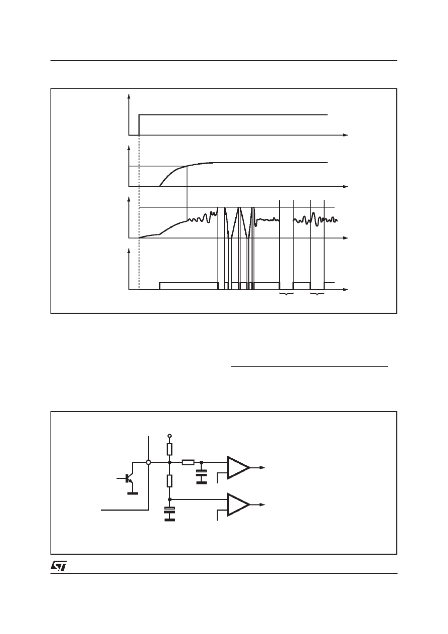
Figure 12: Diagnostics circuit.
Figure 13: Clipping Detection Waveforms.
TDA7385
8/12
t
t
t
MUTE PIN
VOLTAGE
Vs
OUTPUT
WAVEFORM
Vpin 25
WAVEFORM
SHORT TO GND
OR TO Vs
D95AU304
CLIPPING
THERMAL
PROXIMITY
ST-BY PIN
VOLTAGE
t
Figure 14: Diagnostics Waveforms.
reached.
As various kind of diagnostics information is avail-
able at pin 25 (CLIPPING, SHORTS AND OVER-
HEATING), it may be necessary to operate some
distinctions on order to treat each event sepa-
rately. This could be achieved by taking into ac-
count the intrinsically different timing of the diag-
nostics output under each circumstance.
In fact, clipping will produce pulses normally
much shorter than those present under faulty con-
ditions. An example of circuit able to distinguish
between the two occurrences is shown by fig. 15.
STABILITY AND LAYOUT CONSIDERATIONS
If properly layouted and hooked to standard car-
radio speakers, the TDA7385 will be intrinsically
stable with no need of external compensations
CLIP DET. (TO GAIN
COMPRESSOR/
TONE CONTROL)
T1
25
D95AU305
TDA7385
+
-
VREF
VREF1
T2
FAULT, THERMAL SHUTDOWN
(TO POWER SUPPLY
SECTION,
µ
P VOLTAGE
REGULATOR, FLASHING SYSTEM)
+
-
VREF2
T1 << T2
VREF
≥
VREF1 >> VREF2
Figure 15.
TDA7385
9/12

such as output R-C cells. Due to the high number
of channels involved, this translates into a very
remarkable components saving if compared to
similar devices on the market.
To simplify pc-board layout designs, each ampli-
fier stage has its own power ground externally ac-
cessible (pins 2,8,18,24) and one supply voltage
pin for each couple of them.
Even more important, this makes it possible to
achieve the highest possible degree of separation
among the channels, with remarkable benefits in
terms of cross-talk and distortion features.
About the layout grounding, it is particularly im-
portant to connect the AC-GND capacitor (C
5
) to
the signal GND, as close as possible to the audio
inputs ground: this will guarantee high rejection of
any common mode spurious signals.
The SVR capacitor (C
6
) has also to be connected
to the signal GND.
Supply filtering elements (C
7
, C
8
) have naturally
to be connected to the power-ground and located
as close as possible to the Vs pins.
Pin 1, which is mechanically attached to the de-
vice’s tab, needs to be tied to the cleanest power
ground point in the pc-board, which is generally
near the supply filtering capacitors.
TDA7385
10/12
Flexiwatt25
DIM.
mm
inch
MIN.
TYP.
MAX.
MIN.
TYP.
MAX.
A
4.45
4.50
4.65
0.175
0.177
0.183
B
1.80
1.90
2.00
0.070
0.074
0.079
C
1.40
0.055
D
0.75
0.90
1.05
0.029
0.035
0.041
E
0.37
0.39
0.42
0.014
0.015
0.016
F (1)
0.57
0.022
G
0.80
1.00
1.20
0.031
0.040
0.047
G1
23.75
24.00
24.25
0.935
0.945
0.955
H (2)
28.90
29.23
29.30
1.138
1.150
1.153
H1
17.00
0.669
H2
12.80
0.503
H3
0.80
0.031
L (2)
22.07
22.47
22.87
0.869
0.884
0.904
L1
18.57
18.97
19.37
0.731
0.747
0.762
L2 (2)
15.50
15.70
15.90
0.610
0.618
0.626
L3
7.70
7.85
7.95
0.303
0.309
0.313
L4
5
0.197
L5
3.5
0.138
M
3.70
4.00
4.30
0.145
0.157
0.169
M1
3.60
4.00
4.40
0.142
0.157
0.173
N
2.20
0.086
O
2
0.079
R
1.70
0.067
R1
0.5
0.02
R2
0.3
0.12
R3
1.25
0.049
R4
0.50
0.019
V
5
°
(Typ.)
V1
3
°
(Typ.)
V2
20
°
(Typ.)
V3
45
°
(Typ.)
(1): dam-bar protusion not included
(2): molding protusion included
H3
R4
G
V
G1
L2
H1
H
F
M1
L
FLEX25ME
V3
O
L3
L4
H2
R3
N
V2
R
R2
R2
C
B
L1
M
R1
L5
R1
R1
E
D
A
V
V1
V1
OUTLINE AND
MECHANICAL DATA
TDA7385
11/12

Information furnished is believed to be accurate and reliable. However, STMicroelectronics assumes no responsibility for the consequences
of use of such information nor for any infringement of patents or other rights of third parti es which may result from its use. No license is
granted by implication or otherwise under any patent or patent rights of STMicroelectronics. Specification mentioned in this publication are
subject to change without notice. This publication supersedes and replaces all information previously supplied. STMicroelectronics products
are not authorized for use as critical components in life support devices or systems without express written approval of STMicroelectronics.
The ST logo is a registered trademark of STMicroelectronics
2001 STMicroelectronics – Printed in Italy – All Rights Reserved
STMicroelectronics GROUP OF COMPANIES
Australia - Brazil - China - Finland - France - Germany - Hong Kong - India - Italy - Japan - Malaysia - Malta - Morocco -
Singapore - Spain - Sweden - Switzerland - United Kingdom - U.S.A.
http://www.st.com
TDA7385
12/12
Wyszukiwarka
Podobne podstrony:
TDA7388 STMicroelectronics elenota pl
TDA7383 STMicroelectronics elenota pl
TDA7386 STMicroelectronics elenota pl (2)
TDA7381 STMicroelectronics elenota pl
TDA7382 STMicroelectronics elenota pl
TDA7389A STMicroelectronics elenota pl
TDA7386 STMicroelectronics elenota pl (1)
TDA7566 STMicroelectronics elenota pl
TDA7266M STMicroelectronics elenota pl
TDA7850 STMicroelectronics elenota pl
TDA7490LSA STMicroelectronics elenota pl
TDA1908 STMicroelectronics elenota pl (1)
TDA7233 STMicroelectronics elenota pl
TDA7231A STMicroelectronics elenota pl
TDA7360 STMicroelectronics elenota pl
TDA7490SA STMicroelectronics elenota pl
TDA7370B STMicroelectronics elenota pl
TDA2007A STMicroelectronics elenota pl
więcej podobnych podstron