November 2008
Rev 5
1/18
1
TDA7850
4 x 50 W MOSFET quad bridge power amplifier
Features
■
High output power capability:
– 4 x 50 W/4
Ω max.
– 4 x 30 W/4
Ω @ 14.4 V, 1 kHz, 10 %
– 4 x 80 W/2
Ω max.
– 4 x 55 W/2
Ω @ 14.4V, 1 kHz, 10 %
■
MOSFET output power stage
■
Excellent 2
Ω driving capability
■
Hi-Fi class distortion
■
Low output noise
■
ST-BY function
■
Mute function
■
Automute at min. supply voltage detection
■
Low external component count:
– Internally fixed gain (26 dB)
– No external compensation
– No bootstrap capacitors
■
On board 0.35 A high side driver
Protections:
■
Output short circuit to gnd, to V
s
, across the
load
■
Very inductive loads
■
Overrating chip temperature with soft thermal
limiter
■
Output DC offset detection
■
Load dump voltage
■
Fortuitous open gnd
■
Reversed battery
■
ESD
Description
The TDA7850 is a breakthrough MOSFET
technology class AB audio power amplifier in
Flexiwatt 25 package designed for high power car
radio. The fully complementary P-Channel/N-
Channel output structure allows a rail to rail
output voltage swing which, combined with high
output current and minimized saturation losses
sets new power references in the car-radio field,
with unparalleled distortion performances.
The TDA7850 integrates a DC offset detector.
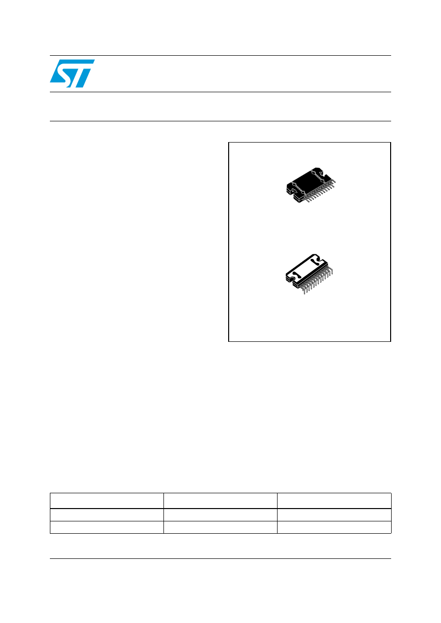
Flexiwatt25
(Vertical)
Flexiwatt25
(Horizontal)
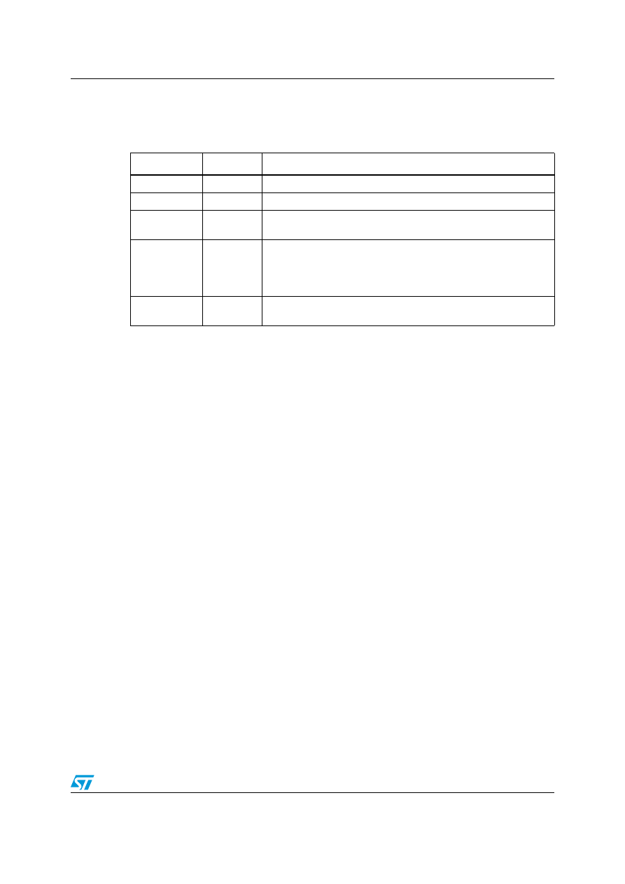
Table 1.
Device summary
Order code
Package
Packing
TDA7850
Flexiwatt25 (Vertical)
Tube
TDA7850H
Flexiwatt25 (Horizontal
Tube

Contents
TDA7850
Contents
Block diagram and application circuit . . . . . . . . . . . . . . . . . . . . . . . . . . . 5
Standard test and application circuit . . . . . . . . . . . . . . . . . . . . . . . . . . . . . 5
Absolute maximum ratings . . . . . . . . . . . . . . . . . . . . . . . . . . . . . . . . . . . . . 7

TDA7850
List of tables
List of tables

List of figures
TDA7850
List of figures
Components and top copper layer of the
Figure 2
. . . . . . . . . . . . . . . . . . . . . . . . . . . . . . . 10
Figure 2
. . . . . . . . . . . . . . . . . . . . . . . . . . . . . . . . . . . . . . . . . . . . . . . 10
Output power vs. supply voltage (R
L
= 4
Ω) . . . . . . . . . . . . . . . . . . . . . . . . . . . . . . . . . . . . 11
Output power vs. supply voltage (R
L
= 2
Ω) . . . . . . . . . . . . . . . . . . . . . . . . . . . . . . . . . . . . 11
Distortion vs. output power (R
L
= 4
Ω). . . . . . . . . . . . . . . . . . . . . . . . . . . . . . . . . . . . . . . . . 11
Distortion vs. output power (R
L
= 2
Ω). . . . . . . . . . . . . . . . . . . . . . . . . . . . . . . . . . . . . . . . . 11
= 4
Ω) . . . . . . . . . . . . . . . . . . . . . . . . . . . . . . . . . . . . . . . . . . . 11
= 2
Ω) . . . . . . . . . . . . . . . . . . . . . . . . . . . . . . . . . . . . . . . . . . . 12
Power dissipation and efficiency vs. output power (R
L
= 4
Ω, SINE) . . . . . . . . . . . . . . . . . 12
Power dissipation and efficiency vs. output power (R
L
= 2
Ω, SINE) . . . . . . . . . . . . . . . . . 12
Power dissipation vs. output power (R
= 4
Ω, audio program simulation) . . . . . . . . . . . . . 13
Power dissipation vs. output power (R
= 2
Ω, audio program simulation) . . . . . . . . . . . . . 13
TDA7850
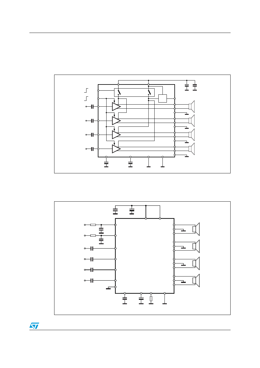
Block diagram and application circuit
1
Block diagram and application circuit
1.1 Block
diagram
Figure 1.
Block diagram
1.2
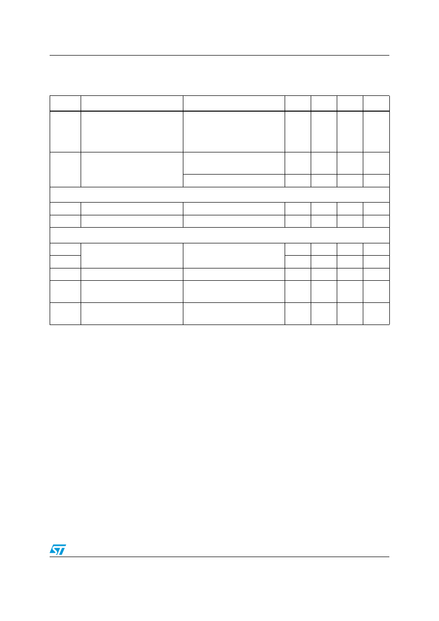
Standard test and application circuit
Figure 2.
Standard test and application circuit
IN1
0.1
μF
MUTE
ST-BY
IN2
0.1
μF
OUT1+
OUT1-
OUT2+
OUT2-
PW-GND
IN3
0.1
μF
IN4
0.1
μF
OUT3+
OUT3-
OUT4+
OUT4-
PW-GND
PW-GND
PW-GND
D94AU158D
AC-GND
0.47
μF
47
μF
SVR
TAB
S-GND
Vcc1
Vcc2
100nF
470
μF
HSD/V
OFF_DET
HSD
IN1
0.1
μF
C9
1
μF
IN2
C2 0.1
μF
OUT1
OUT2
IN3
C3 0.1
μF
IN4
C4 0.1
μF
OUT3
OUT4
D95AU335C
C5
0.47
μF
C6
47
μF
SVR
TAB
Vcc1-2
Vcc3-4
C8
0.1
μF
C7
2200
μF
C10
1
μF
ST-BY
R1
10K
R3
*)
R2
47K
MUTE
C1
14
15
12
11
22
4
13
S-GND
16
10
25
1
HSD/OD
6
20
9
8
7
5
2
3
17
18
19
21
24
23
*) R3 = 10k
Ω to be placed when pin 25 is used as offset detector.
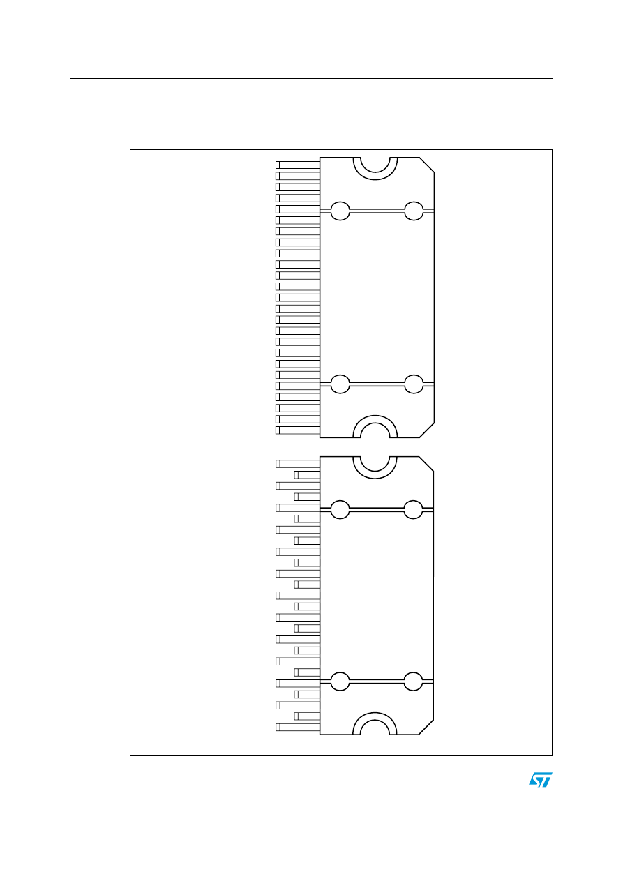
Pin description
TDA7850
2 Pin
description
Figure 3.
Pin connection (top view)
D94AU159A
TAB
P-GND2
OUT2-
ST-BY
OUT2+
V
CC
OUT1-
P-GND1
OUT1+
SVR
IN1
IN2
S-GND
IN4
IN3
AC-GND
OUT3+
P-GND3
OUT3-
V
CC
OUT4+
MUTE
OUT4-
P-GND4
HSD
1
25
D06AU1655
TAB
P-GND2
OUT2-
ST-BY
OUT2+
V
CC
OUT1-
P-GND1
OUT1+
SVR
IN1
IN2
S-GND
IN4
IN3
AC-GND
OUT3+
P-GND3
OUT3-
V
CC
OUT4+
MUTE
OUT4-
P-GND4
HSD
1
25
Vertical
Horizontal
TDA7850
Electrical specifications
3 Electrical
specifications
3.1
Absolute maximum ratings
3.2 Thermal
data
Table 2.
Absolute maximum ratings
Symbol
Parameter
Value
Unit
V
S
Operating supply voltage
18
V
V
S (DC)
DC supply voltage
28
V
V
S (pk)
Peak supply voltage (for t = 50 ms)
50
V
I
O
Output peak current
repetitive (duty cycle 10 % at f = 10 Hz)
non repetitive (t = 100
μs)
9
10
A
A
P
tot
Power dissipation T
case
= 70 °C
80
W
T
j
Junction temperature
150
°C
T
stg
Storage temperature
-55 to 150
°C
Table 3.
Thermal data
Symbol
Parameter
Value
Unit
R
th j-case
Thermal resistance junction to case
Max.
1
°C/W
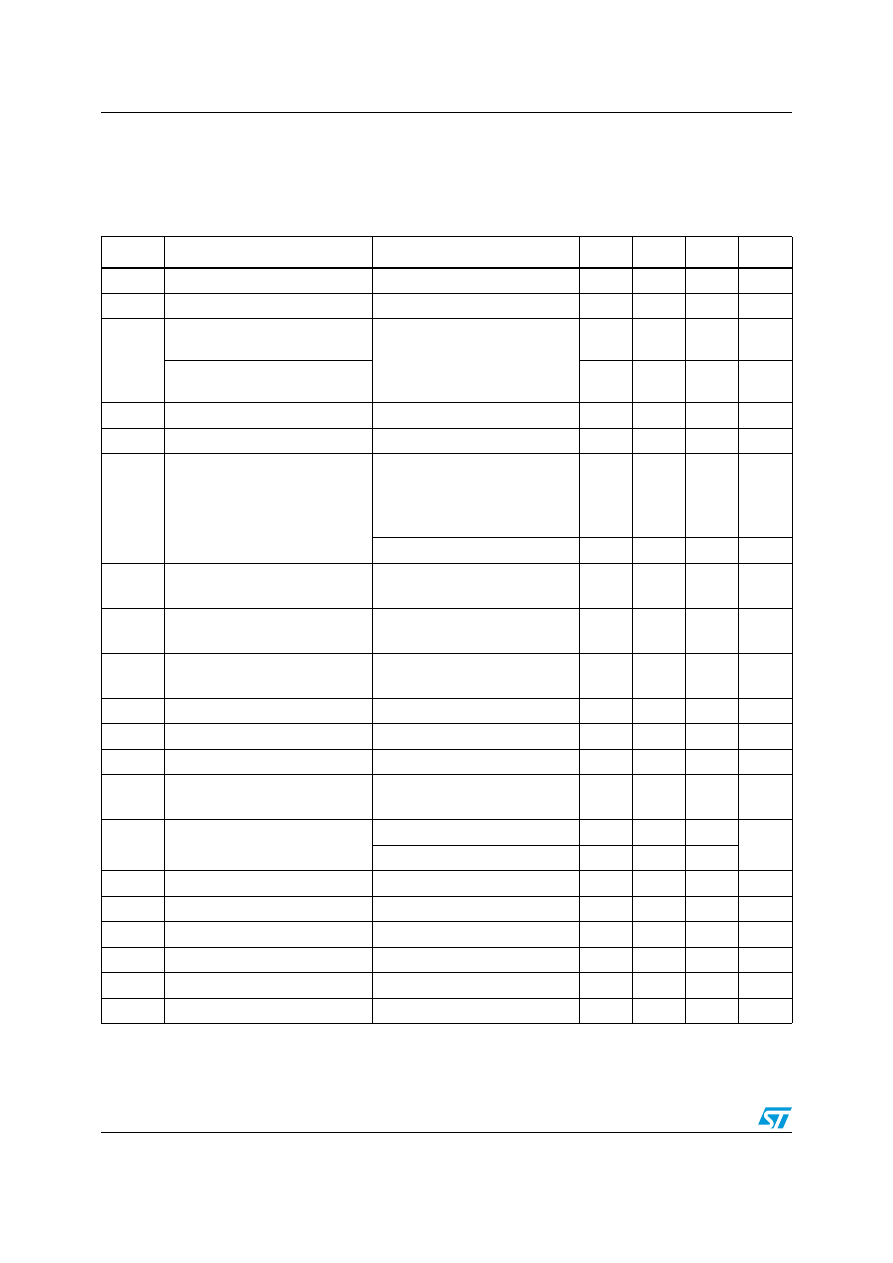
Electrical specifications
TDA7850
3.3 Electrical
characteristics
Table 4.
Electrical characteristics
(Refer to the test and application diagram, V
S
= 14.4 V; R
L
= 4
Ω; R
g
= 600
Ω; f = 1 kHz;
T
amb
= 25 °C; unless otherwise specified).
Symbol
Parameter
Test condition
Min.
Typ.
Max.
Unit
I
q1
Quiescent current
R
L
=
∞
100
180
280
mA
V
OS
Output offset voltage
Play mode / Mute mode
±50
mV
dV
OS
During mute ON/OFF output
offset voltage
ITU R-ARM weighted
see
-10
+10
mV
During Standby ON/OFF output
offset voltage
-10
+10
mV
G
v
Voltage gain
25
26
27
dB
dG
v
Channel gain unbalance
±1
dB
P
o
Output
power
V
S
= 13.2 V; THD = 10 %
V
S
= 13.2 V; THD = 1 %
V
S
= 14.4 V; THD = 10 %
V
S
= 14.4 V; THD = 1 %
23
16
28
20
25
19
30
23
W
V
S
= 14.4 V; THD = 10 %, 2
Ω
50
55
W
P
o max.
Max. output power
(1)
V
S
= 14.4 V; R
L
= 4
Ω
V
S
= 14.4 V; R
L
= 2
Ω
50
85
W
THD
Distortion
P
o
= 4W
P
o
= 15W; R
L
= 2
Ω
0.006
0.015
0.02
0.03
%
e
No
Output
noise
"A" Weighted
Bw = 20 Hz to 20 kHz
35
50
50
70
μV
SVR
Supply voltage rejection
f = 100 Hz; V
r
= 1Vrms
50
75
dB
f
ch
High cut-off frequency
P
O
= 0.5 W
100
300
KHz
R
i
Input impedance
80
100
120
K
Ω
C
T
Cross talk
f = 1 kHz P
O
= 4 W
f = 10 kHz P
O
= 4 W
60
70
60
-
-
dB
I
SB
Standby current consumption
V
ST-BY
= 1.5 V
20
μA
V
ST-BY
= 0 V
10
I
pin5
ST-BY pin current
V
ST-BY
= 1.5 V to 3.5 V
±1
μA
V
SB out
Standby out threshold voltage
(Amp: ON)
2.75
V
V
SB in
Standby in threshold voltage
(Amp: OFF)
1.5
V
A
M
Mute attenuation
P
Oref
= 4 W
80
90
dB
V
M out
Mute out threshold voltage
(Amp: Play)
3.5
V
V
M in
Mute in threshold voltage
(Amp: Mute)
1.5
V
TDA7850
Electrical specifications
V
AM in
V
S
automute threshold
(Amp: Mute)
Att
≥
80 dB; P
Oref
= 4 W
(Amp: Play)
Att < 0.1 dB; P
O
= 0. 5W
6.5
7
7.5
8
V
I
pin23
Muting pin current
V
MUTE
= 1.5 V
(Sourced Current)
7
12
18
μA
V
MUTE
= 3.5 V
-5
18
μA
HSD section
V
dropout
Dropout voltage
I
O
= 0.35 A; V
S
= 9 to 16 V
0.25
0.6
V
I
prot
Current limits
400
800
mA
Offset detector (Pin 25)
V
M_ON
Mute voltage for DC offset
detection enabled
V
ST-BY
= 5 V
8
V
V
M_OFF
6
V
V
OFF
Detected differential output offset V
ST-BY
= 5 V; V
mute
= 8 V
±2
±3
±4
V
V
25_T
Pin 25 voltage for detection =
TRUE
V
ST-BY
= 5 V; V
mute
= 8 V
V
OFF
> ±4 V
0
1.5
V
V
25_F
Pin 25 Voltage for detection =
FALSE
V
ST-BY
= 5 V; V
mute
= 8 V
V
OFF
> ±2 V
12
V
1.
Saturated square wave output.
Table 4.
Electrical characteristics (continued)
(Refer to the test and application diagram, V
S
= 14.4 V; R
L
= 4
Ω; R
g
= 600
Ω; f = 1 kHz;
T
amb
= 25 °C; unless otherwise specified).
Symbol
Parameter
Test condition
Min.
Typ.
Max.
Unit
Electrical specifications
TDA7850
Figure 4.
Components and top copper layer of the
.
Figure 5.
Bottom copper layer
TDA7850
Electrical specifications
3.4
Electrical characteristic curves
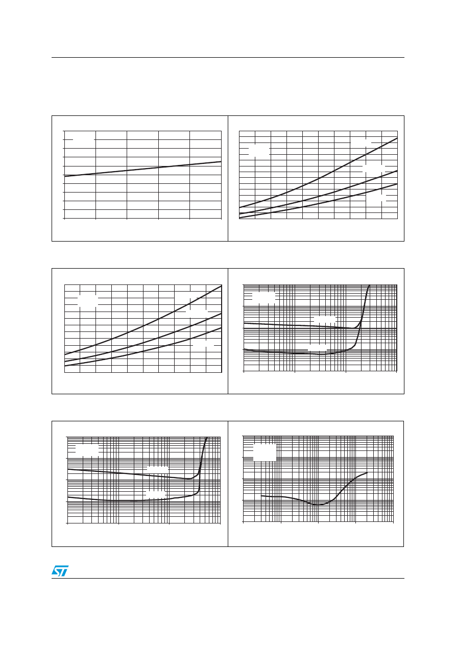
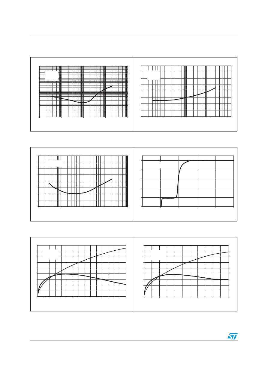
Figure 6.
Quiescent current vs. supply
voltage
Figure 7.
Output power vs. supply voltage
(R
L
= 4
Ω)
Figure 8.
Output power vs. supply voltage
(R
L
= 2
Ω)
Figure 9.
Distortion vs. output power
(R
L
= 4
Ω)
Figure 10.
Distortion vs. output power
(R
L
= 2
Ω)
Figure 11.
Distortion vs. frequency
(R
L
= 4
Ω)
AC00064
Vs (V)
100
110
120
130
140
150
160
170
180
190
200
8
10
12
14
16
18
Vi = 0
RL =
∞
Id (mA)
5
10
15
20
25
30
35
40
45
50
55
60
65
70
75
80
8
9
10
11
12
13
14
15
16
17
18
P
o
(W)
V
s
(V)
R
L
= 4
Ω
f = 1 KHz
Po-max
THD= 10%
THD= 1%
AC00064
AC00066
0
10
20
30
40
50
60
70
80
90
100
110
120
130
8
9
10
11
12
13
14
15
16
17
18
Vs (V)
Po (W)
Po-max
THD=10%
THD=1%
R
L
= 2
Ω
f = 1 KHz
AC00067
0.001
0.01
0.1
1
10
0.1
1
10
100
P
o
(W)
THD (%)
V
S
= 14.4 V
R
L
= 4
Ω
f = 1 KHz
f = 10 KHz
AC00068
0.001
0.01
0.1
1
10
0.1
1
10
100
Po (W)
THD (%)
V
S
= 14.4 V
RL = 2Ω
f = 10 KHz
f = 1 KHz
AC00069
0.001
0.01
0.1
1
10
10
100
1000
10000
100000
f (Hz)
THD (%)
V
S
= 14.4 V
R
L
= 4
Ω
P
o
= 4 W
Electrical specifications
TDA7850
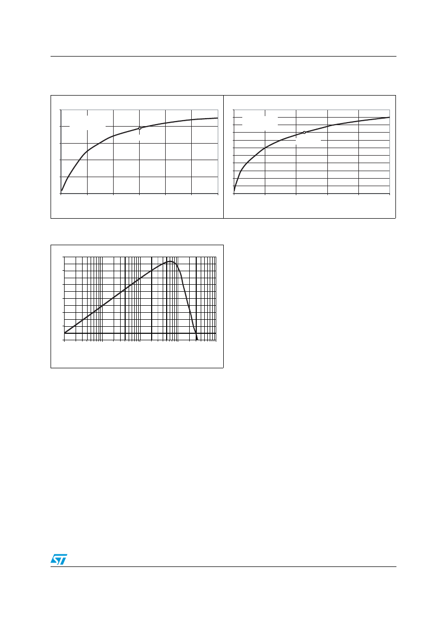
Figure 12.
Distortion vs. frequency
(R
L
= 2
Ω)
Figure 13.
Crosstalk vs. frequency
Figure 14.
Supply voltage rejection vs.
frequency
Figure 15.
Output attenuation vs. supply
voltage
Figure 16.
Power dissipation and efficiency
vs. output power (R
L
= 4
Ω, SINE)
Figure 17.
Power dissipation and efficiency
vs. output power (R
L
= 2
Ω, SINE)
AC00070
0.001
0.01
0.1
1
10
10
100
1000
10000
100000
f (Hz)
THD (%)
V
S
= 14.4 V
R
L
= 2
Ω
P
o
= 8 W
-100
-90
-80
-70
-60
-50
-40
-30
-20
10
100
1000
10000
100000
R
L
= 4
Ω
P
o
= 4 W
R
g
= 600
Ω
f (Hz)
CROSSTALK (dB)
AC00071
AC00072
-100
-90
-80
-70
-60
-50
-40
-30
-20
10
100
1000
10000
100000
f (Hz)
SVR (dB)
Rg = 600Ω
Vripple = 1 Vrms
AC00073
-100
-80
-60
-40
-20
0
5
6
7
8
9
10
Vs (V)
OUTPUT ATTN (dB)
R
L
= 4
Ω
P
o
= 4 W ref
AC00074
0
10
20
30
40
50
60
70
80
90
0
2
4
6
8
10
12
14
16
18
20
22
24
26
28
30
P
tot
(W)
η (%)
P
o
(W)
0
10
20
30
40
50
60
70
80
90
P
tot
η
V
S
= 14.4 V
R
L
= 4 x 4
Ω
f = 1 KHz SINE
AC00075
0
20
40
60
80
100
120
140
160
180
0
5
10
15
20
25
30
35
40
45
50
55
0
10
20
30
40
50
60
70
80
90
Ptot (W)
η (%)
P
o
(W)
P
tot
η
V
S
= 14.4 V
R
L
= 4 x 2
Ω
f = 1 KHz SINE
TDA7850
Electrical specifications
Figure 18.
Power dissipation vs. output power
(R
L
= 4
Ω, audio program simulation)
Figure 19.
Power dissipation vs. output power
(R
L
= 2
Ω, audio program simulation)
Figure 20.
ITU R-ARM frequency response,
weighting filter for transient pop
AC00076
5
10
15
20
25
30
0
1
2
3
4
5
6
V
S
= 13.2 V
R
L
= 4 x 4
Ω
GAUSSIAN NOISE
CLIP START
P
tot
(W)
P
o
(W)
AC00077
5
10
15
20
25
30
35
40
45
50
55
60
0
2
4
6
8
10
V
S
= 13.2 V
R
L
= 4 x 2
Ω
GAUSSIAN NOISE
CLIP START
P
tot
(W)
P
o
(W)
Output attenuation (dB)
-50
-40
-30
-20
-10
0
10
10
100
1000
10000
100000
Hz
AC00343

Application hints
TDA7850
4 Application
hints
Referred to the circuit of
4.1 SVR
Besides its contribution to the ripple rejection, the SVR capacitor governs the turn ON/OFF
time sequence and, consequently, plays an essential role in the pop optimization during
ON/OFF transients. To conveniently serve both needs, Its minimum recommended value
is 10µF.
4.2 Input
stage
The TDA7850's inputs are ground-compatible and can stand very high input signals (±
8Vpk) without any performance degradation.
If the standard value for the input capacitors (0.1µF) is adopted, the low frequency cut-off
will amount to 16 Hz.
4.3 Standby
and
muting
Standby and Muting facilities are both CMOS compatible. In absence of true CMOS ports or
microprocessors, a direct connection to Vs of these two pins is admissible but a 470k
Ω
equivalent resistance should be present between the power supply and the muting and
ST-BY pins.
R-C cells have always to be used in order to smooth down the transitions for preventing any
audible transient noises.
About the standby, the time constant to be assigned in order to obtain a virtually pop-free
transition has to be slower than 2.5 V/ms.
4.4 DC
offset
detector
The TDA7850 integrates a DC offset detector to avoid that an anomalous DC offset on the
inputs of the amplifier may be multiplied by the gain and result in a dangerous large offset on
the outputs which may lead to speakers damage for overheating. The feature is enabled by
the MUTE pin (according to table 3) and works with the amplifier unmuted and with no signal
on the inputs.
The DC offset detection is signaled out on the HSD pin. To ensure the correct functionality of
the Offset Detector it is necessary to connect a pulldown 10 kW resistor between HSD and
ground.
4.5 Heatsink
definition
Under normal usage (4 Ohm speakers) the heatsink's thermal requirements have to be
deduced from
, which reports the simulated power dissipation when real
music/speech programmes are played out. Noise with gaussian-distributed amplitude was
employed for this simulation. Based on that, frequent clipping occurrence (worst-case) will
cause P
diss
= 26 W. Assuming T
amb
= 70 °C and T
CHIP
= 150 °C as boundary conditions, the
heatsink's thermal resistance should be approximately 2°C/W. This would avoid any thermal
shutdown occurrence even after long-term and full-volume operation.
TDA7850
Package information
5 Package
information
In order to meet environmental requirements, ST (also) offers these devices in ECOPACK
®
packages. ECOPACK
®
packages are lead-free. The category of second Level Interconnect
is marked on the package and on the inner box label, in compliance with JEDEC Standard
JESD97. The maximum ratings related to soldering conditions are also marked on the inner
box label.
ECOPACK is an ST trademark. ECOPACK specifications are available at: www.st.com.
Figure 21.
Flexiwatt25 (vertical) mechanical data and package dimensions
OUTLINE AND
MECHANICAL DATA
DIM.
mm
inch
MIN.
TYP.
MAX.
MIN.
TYP.
MAX.
A
4.45
4.50
4.65
0.175
0.177
0.183
B
1.80
1.90
2.00
0.070
0.074
0.079
C
1.40
0.055
D
0.75
0.90
1.05
0.029
0.035
0.041
E
0.37
0.39
0.42
0.014
0.015
0.016
F (1)
0.57
0.022
G
0.80
1.00
1.20
0.031
0.040
0.047
G1
23.75
24.00
24.25
0.935
0.945
0.955
H (2)
28.90
29.23
29.30
1.139
1.150
1.153
H1
17.00
0.669
H2
12.80
0.503
H3
0.80
0.031
L (2)
22.07
22.47
22.87
0.869
0.884
0.904
L1
18.57
18.97
19.37
0.731
0.747
0.762
L2 (2)
15.50
15.70
15.90
0.610
0.618
0.626
L3
7.70
7.85
7.95
0.303
0.309
0.313
L4
5
0.197
L5
3.5
0.138
M
3.70
4.00
4.30
0.145
0.157
0.169
M1
3.60
4.00
4.40
0.142
0.157
0.173
N
2.20
0.086
O
2
0.079
R
1.70
0.067
R1
0.5
0.02
R2
0.3
0.12
R3
1.25
0.049
R4
0.50
0.019
V1
3˚ (Typ.)
V
5˚ (T p.)
V2
20˚ (Typ.)
V3
45˚ (Typ.)
(2): molding protusion included
(1): dam-bar protusion not included
Flexiwatt25 (vertical)
H3
R4
G
V
G1
L2
H1
H
F
M1
L
FLEX25ME
V3
O
L3
L4
H2
R3
N
V2
R
R2
R2
C
B
L1
M
R1
L5
R1
R1
E
D
A
Pin 1
V
V1
V1
7034862
Package information
TDA7850
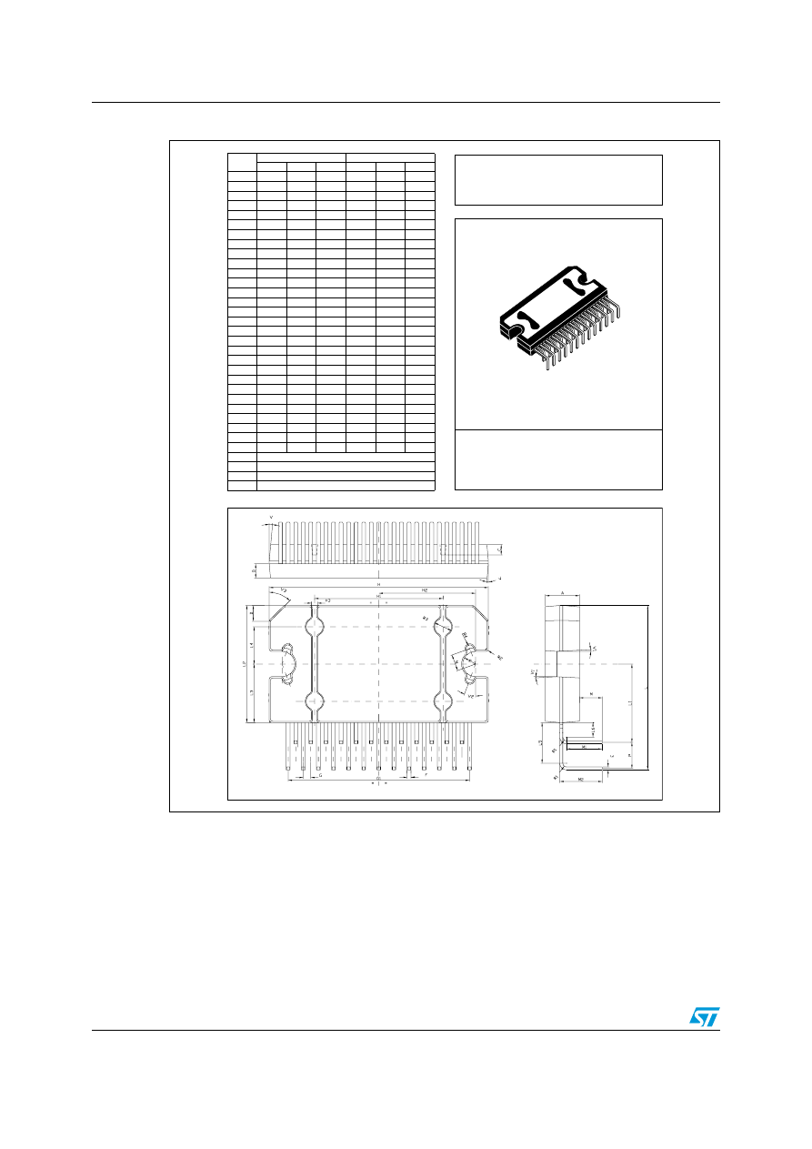
Figure 22.
Flexiwatt25 (horizontal) mechanical data and package dimensions
OUTLINE AND
MECHANICAL DATA
DIM.
mm
inch
MIN.
TYP.
MAX.
MIN.
TYP.
MAX.
A
4.45
4.50
4.65
0.175
0.177
0.183
B
1.80
1.90
2.00
0.070
0.074
0.079
C
1.40
0.055
D
2.00
0.079
E
0.37
0.39
0.42
0.014
0.015
0.016
F (1)
0.57
0.022
G
0.75
1.00
1.25
0.029
0.040
0.049
G1
23.70
24.00
24.30
0.933
0.945
0.957
H (2)
28.90
29.23
29.30
1.139
1.150
1.153
H1
17.00
0.669
H2
12.80
0.503
H3
0.80
0.031
L (2)
21.64
22.04
22.44
0.852
0.868
0.883
L1
10.15
10.5
10.85
0.40
0.413
0.427
L2 (2)
15.50
15.70
15.90
0.610
0.618
0.626
L3
7.70
7.85
7.95
0.303
0.309
0.313
L4
5
0.197
L5
5.15
5.45
5.85
0.203
0.214
0.23
L6
1.80
1.95
2.10
0.070
0.077
0.083
M
2.75
3.00
3.50
0.108
0.118
0.138
M1
4.73
0.186
M2
5.61
0.220
N
2.20
0.086
P
3.20
3.50
3.80
0.126
0.138
0.15
R
1.70
0.067
R1
0.50
0.02
R2
0.30
0.12
R3
1.25
0.049
R4
0.50
0.02
V
5˚ (Typ.)
V1
3˚ (Typ.)
V2
20˚ (Typ.)
V3
45˚ (Typ.)
Flexiwatt25
(Horizontal)
7399733 A
(1): dam-bar protusion not included; (2): molding protusion included
TDA7850
Revision history
6 Revision
history
Table 5.
Document revision history
Date
Revision
Changes
22-Nov-2006
1
Initial release.
27-Feb-2007
2
Added
Chapter 3.4: Electrical characteristic curves
.
09-Oct-2007
3
Updated the values for the dV
OS
and I
q1
.
Added
12-Sep-2008
4
Updated
Figure 2: Standard test and application circuit
.
Updated
Section 4.4: DC offset detector
Updated the values of V
OS
and THD parameters on the
.
07-Nov-2008
5

TDA7850
Please Read Carefully:
Information in this document is provided solely in connection with ST products. STMicroelectronics NV and its subsidiaries (“ST”) reserve the
right to make changes, corrections, modifications or improvements, to this document, and the products and services described herein at any
time, without notice.
All ST products are sold pursuant to ST’s terms and conditions of sale.
Purchasers are solely responsible for the choice, selection and use of the ST products and services described herein, and ST assumes no
liability whatsoever relating to the choice, selection or use of the ST products and services described herein.
No license, express or implied, by estoppel or otherwise, to any intellectual property rights is granted under this document. If any part of this
document refers to any third party products or services it shall not be deemed a license grant by ST for the use of such third party products
or services, or any intellectual property contained therein or considered as a warranty covering the use in any manner whatsoever of such
third party products or services or any intellectual property contained therein.
UNLESS OTHERWISE SET FORTH IN ST’S TERMS AND CONDITIONS OF SALE ST DISCLAIMS ANY EXPRESS OR IMPLIED
WARRANTY WITH RESPECT TO THE USE AND/OR SALE OF ST PRODUCTS INCLUDING WITHOUT LIMITATION IMPLIED
WARRANTIES OF MERCHANTABILITY, FITNESS FOR A PARTICULAR PURPOSE (AND THEIR EQUIVALENTS UNDER THE LAWS
OF ANY JURISDICTION), OR INFRINGEMENT OF ANY PATENT, COPYRIGHT OR OTHER INTELLECTUAL PROPERTY RIGHT.
UNLESS EXPRESSLY APPROVED IN WRITING BY AN AUTHORIZED ST REPRESENTATIVE, ST PRODUCTS ARE NOT
RECOMMENDED, AUTHORIZED OR WARRANTED FOR USE IN MILITARY, AIR CRAFT, SPACE, LIFE SAVING, OR LIFE SUSTAINING
APPLICATIONS, NOR IN PRODUCTS OR SYSTEMS WHERE FAILURE OR MALFUNCTION MAY RESULT IN PERSONAL INJURY,
DEATH, OR SEVERE PROPERTY OR ENVIRONMENTAL DAMAGE. ST PRODUCTS WHICH ARE NOT SPECIFIED AS "AUTOMOTIVE
GRADE" MAY ONLY BE USED IN AUTOMOTIVE APPLICATIONS AT USER’S OWN RISK.
Resale of ST products with provisions different from the statements and/or technical features set forth in this document shall immediately void
any warranty granted by ST for the ST product or service described herein and shall not create or extend in any manner whatsoever, any
liability of ST.
ST and the ST logo are trademarks or registered trademarks of ST in various countries.
Information in this document supersedes and replaces all information previously supplied.
The ST logo is a registered trademark of STMicroelectronics. All other names are the property of their respective owners.
© 2008 STMicroelectronics - All rights reserved
STMicroelectronics group of companies
Australia - Belgium - Brazil - Canada - China - Czech Republic - Finland - France - Germany - Hong Kong - India - Israel - Italy - Japan -
Malaysia - Malta - Morocco - Singapore - Spain - Sweden - Switzerland - United Kingdom - United States of America
www.st.com
Document Outline
- Table 1. Device summary
- 1 Block diagram and application circuit
- 2 Pin description
- 3 Electrical specifications
- 3.1 Absolute maximum ratings
- 3.2 Thermal data
- 3.3 Electrical characteristics
- 3.4 Electrical characteristic curves
- Figure 6. Quiescent current vs. supply voltage
- Figure 7. Output power vs. supply voltage (RL = 4W)
- Figure 8. Output power vs. supply voltage (RL = 2W)
- Figure 9. Distortion vs. output power (RL = 4W)
- Figure 10. Distortion vs. output power (RL = 2W)
- Figure 11. Distortion vs. frequency (RL = 4W)
- Figure 12. Distortion vs. frequency (RL = 2W)
- Figure 13. Crosstalk vs. frequency
- Figure 14. Supply voltage rejection vs. frequency
- Figure 15. Output attenuation vs. supply voltage
- Figure 16. Power dissipation and efficiency vs. output power (RL = 4W, SINE)
- Figure 17. Power dissipation and efficiency vs. output power (RL = 2W, SINE)
- Figure 18. Power dissipation vs. output power (RL = 4W, audio program simulation)
- Figure 19. Power dissipation vs. output power (RL = 2W, audio program simulation)
- Figure 20. ITU R-ARM frequency response, weighting filter for transient pop
- 4 Application hints
- 5 Package information
- 6 Revision history
Wyszukiwarka
Podobne podstrony:
TDA7851A STMicroelectronics elenota pl
TDA7388 STMicroelectronics elenota pl
TDA7383 STMicroelectronics elenota pl
TDA7566 STMicroelectronics elenota pl
TDA7266M STMicroelectronics elenota pl
TDA7490LSA STMicroelectronics elenota pl
TDA1908 STMicroelectronics elenota pl (1)
TDA7233 STMicroelectronics elenota pl
TDA7231A STMicroelectronics elenota pl
TDA7360 STMicroelectronics elenota pl
TDA7386 STMicroelectronics elenota pl (2)
TDA7385 STMicroelectronics elenota pl
TDA7490SA STMicroelectronics elenota pl
TDA7370B STMicroelectronics elenota pl
TDA2007A STMicroelectronics elenota pl
TDA7266S STMicroelectronics elenota pl
TDA7266D STMicroelectronics elenota pl
TDA7497S STMicroelectronics elenota pl
więcej podobnych podstron