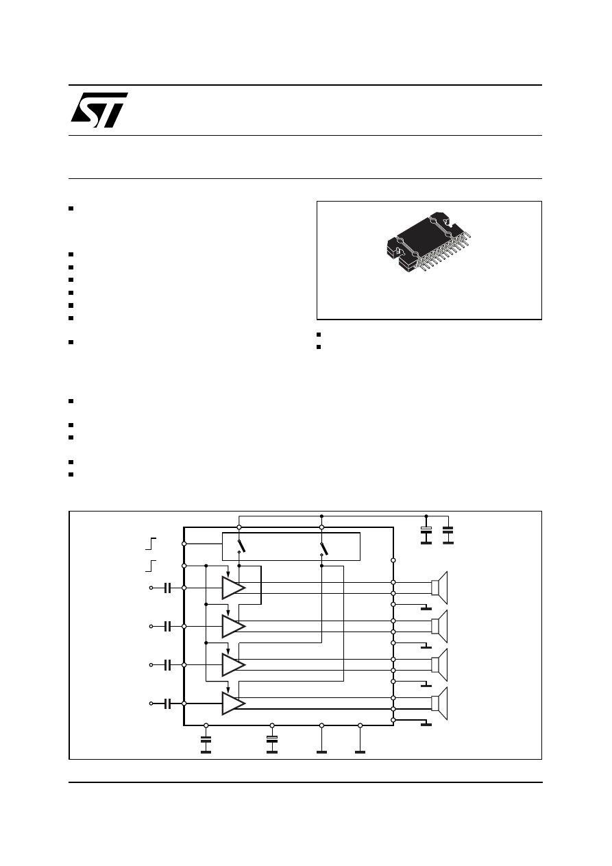
TDA7382
4 x 22W FOUR BRIDGE CHANNELS CAR RADIO AMPLIFIER
HIGH OUTPUT POWER CAPABILITY:
4 x 30W max./4
Ω
EIAJ
4 x 22W/4
Ω
@ 14.4V, 1KHz, 10%
4 x 18.5W/4
Ω
@ 13.2V, 1KHz, 10%
CLIPPING DETECTOR (THD = 10%)
LOW DISTORTION
LOW OUTPUT NOISE
ST-BY FUNCTION
MUTE FUNCTION
AUTOMUTE AT MIN. SUPPLY VOLTAGE DE-
TECTION
LOW EXTERNAL COMPONENT COUNT:
– INTERNALLY FIXED GAIN (26dB)
– NO EXTERNAL COMPENSATION
– NO BOOTSTRAP CAPACITORS
PROTECTIONS:
OUTPUT SHORT CIRCUIT TO GND, TO V
S
,
ACROSS THE LOAD
VERY INDUCTIVE LOADS
OVERRATING CHIP TEMPERATURE WITH
SOFT THERMAL LIMITER
LOAD DUMP VOLTAGE
FORTUITOUS OPEN GND
REVERSED BATTERY
ESD PROTECTION
DESCRIPTION
The TDA7382 is a new technology class AB
Audio Power Amplifier in Flexiwatt 25 package
designed for high end car radio applications.
Thanks to the fully complementary PNP/NPN out-
put configuration the TDA7382 allows a rail to rail
output voltage swing with no need of bootstrap
capacitors. The extremely reduced components
count allows very compact sets. The on-board
clipping detector simplifies gain compression op-
erations.
March 2001
®
ORDERING NUMBER: TDA7382
IN1
0.1
µ
F
MUTE
ST-BY
IN2
0.1
µ
F
OUT1+
OUT1-
OUT2+
OUT2-
PW-GND
IN3
0.1
µ
F
IN4
0.1
µ
F
OUT3+
OUT3-
OUT4+
OUT4-
PW-GND
PW-GND
PW-GND
D98AU818
AC-GND
0.1
µ
F
47
µ
F
SVR
TAB
S-GND
Vcc1
Vcc2
100nF
2.200
µ
F
CLIPPING DET.
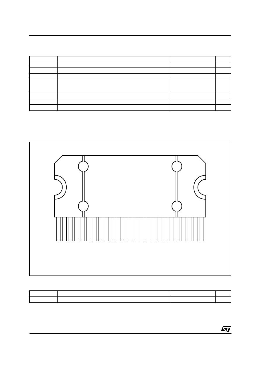
BLOCK AND APPLICATION DIAGRAM
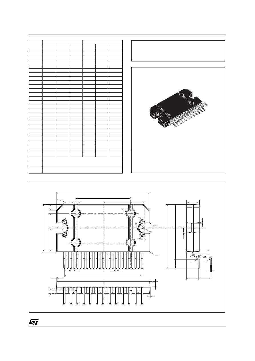
FLEXIWATT25
1/10
D98AU820
TAB
P-GND
OUT2-
ST-BY
OUT2+
V
CC
OUT1-
P-GND1
OUT1+
SVR
IN1
IN2
S-GND
IN4
IN3
AC-GND
OUT3+
P-GND3
OUT3-
V
CC
OUT4+
MUTE
OUT4-
P-GND4
CLIP. DET.
1
25
PIN CONNECTION (Top view)
ABSOLUTE MAXIMUM RATINGS
Symbol
Parameter
Value
Unit
V
CC
Operating Supply Voltage
18
V
V
CC (DC)
DC Supply Voltage
28
V
V
CC (pk)
Peak Supply Voltage (t = 50ms)
50
V
I
O
Output Peak Current:
Repetitive (Duty Cycle 10% at f = 10Hz)
Non Repetitive (t = 100
µ
s)
4.5
5.5
A
A
P
tot
Power dissipation, (T
case
= 70
°
C)
80
W
T
j
Junction Temperature
150
°
C
T
stg
Storage Temperature
– 55 to 150
°
C
THERMAL DATA
Symbol
Parameter
Value
Unit
R
th j-case
Thermal Resistance Junction to Case Max.
1
°
C/W
TDA7382
2/10
ELECTRICAL CHARACTERISTICS (V
S
= 14.4V; f = 1KHz; R
g
= 600
Ω
; R
L
= 4
Ω
; T
amb
= 25
°
C;
Refer to the Test and application circuit (fig.1), unless otherwise specified.)
Symbol
Parameter
Test Condition
Min.
Typ.
Max.
Unit
I
q1
Quiescent Current
85
180
300
mA
V
OS
Output Offset Voltage
100
mV
G
v
Voltage Gain
25
26
27
dB
P
o
Output Power
THD = 10%
THD = 1%
THD = 10%; V
S
= 13.5V
THD = 10%; V
S
= 14V
THD = 5%; V
S
= 14V
THD = 1%; V
S
= 14V
THD = 10%; V
S
= 13.2V
THD = 1%; V
S
= 13.2V
20
16.5
17
19
17
16
17
14
22
18
20
21
19
17
18.5
15
W
W
W
W
W
W
W
W
P
o max
Max. Output Power
EIAJ RULES
27.5
30
W
THD
Distortion
P
o
= 4W
0.04
0.3
%
e
No
Output Noise
"A" Weighted
Bw = 20Hz to 20KHz
50
65
120
150
µ
V
µ
V
SVR
Supply Voltage Rejection
f = 100Hz
50
65
dB
f
cl
Low Cut-Off Frequency
20
Hz
f
ch
High Cut-Off Frequency
75
KHz
R
i
Input Impedance
60
100
130
K
Ω
C
T
Cross Talk
f = 1KHz
50
70
dB
I
SB
St-By Current Consumption
St-By = LOW
20
50
µ
A
V
SB out
St-By OUT Threshold Voltage
(Amp: ON)
3.5
V
V
SB IN
St-By IN Threshold Voltage
(Amp: OFF)
1.5
V
A
M
Mute Attenuation
V
O
= 1Vrms
80
90
dB
V
M out
Mute OUT Threshold Voltage
(Amp: Play)
3.5
V
V
M in
Mute IN Threshold Voltage
(Amp: Mute)
1.5
V
I
m (L)
Muting Pin Current
V
MUTE
= 1.5V
(Source Current)
5
13
16
µ
A
CDL
Clipping Detection THD Level
5
10
15
%
TDA7382
3/10
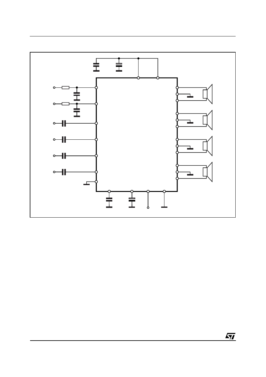
IN1
0.1
µ
F
C9
1
µ
F
IN2
C2 0.1
µ
F
OUT1
OUT2
IN3
C3 0.1
µ
F
IN4
C4 0.1
µ
F
OUT3
OUT4
D98AU819
C5
0.1
µ
F
C6
47
µ
F
SVR
TAB
Vcc1-2
Vcc3-4
C8
0.1
µ
F
C7
2200
µ
F
C10
1
µ
F
ST-BY
R1
10K
R2
47K
MUTE
C1
14
15
12
11
22
4
13
S-GND
16
10
25
1
CLIPPING DET.
6
20
9
8
7
5
2
3
17
18
19
21
24
23
Figure 1: Standard Test and Application Circuit
TDA7382
4/10
TDA7382
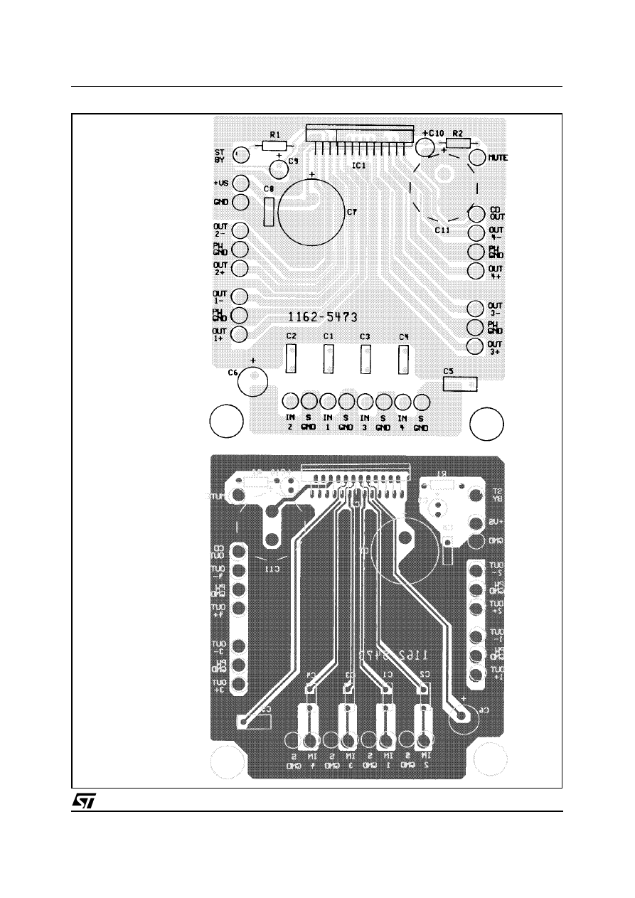
Figure 2: P.C.B. and component layout of the figure 1 (1:1 scale)
COMPONENTS &
TOP COPPER LAYER
BOTTOM COPPER LAYER
TDA7382
5/10
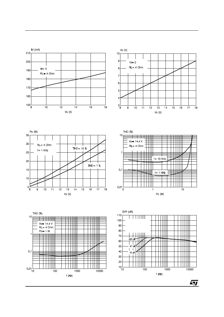
Figure 3: Quiescent Current vs. Supply Voltage
Figure 4: Quiescent Output Voltage vs. Supply
Voltage
Figure 5: Output Power vs. Supply Voltage
Figure 6: Distortion vs. Output Power
Figure 7: Distortion vs. Frequency.
Figure 8: Supply Voltage Rejection vs.
Frequency by varying C6
R
g
= 600
Ω
V
ripple
= 1Vrms
TDA7382
6/10
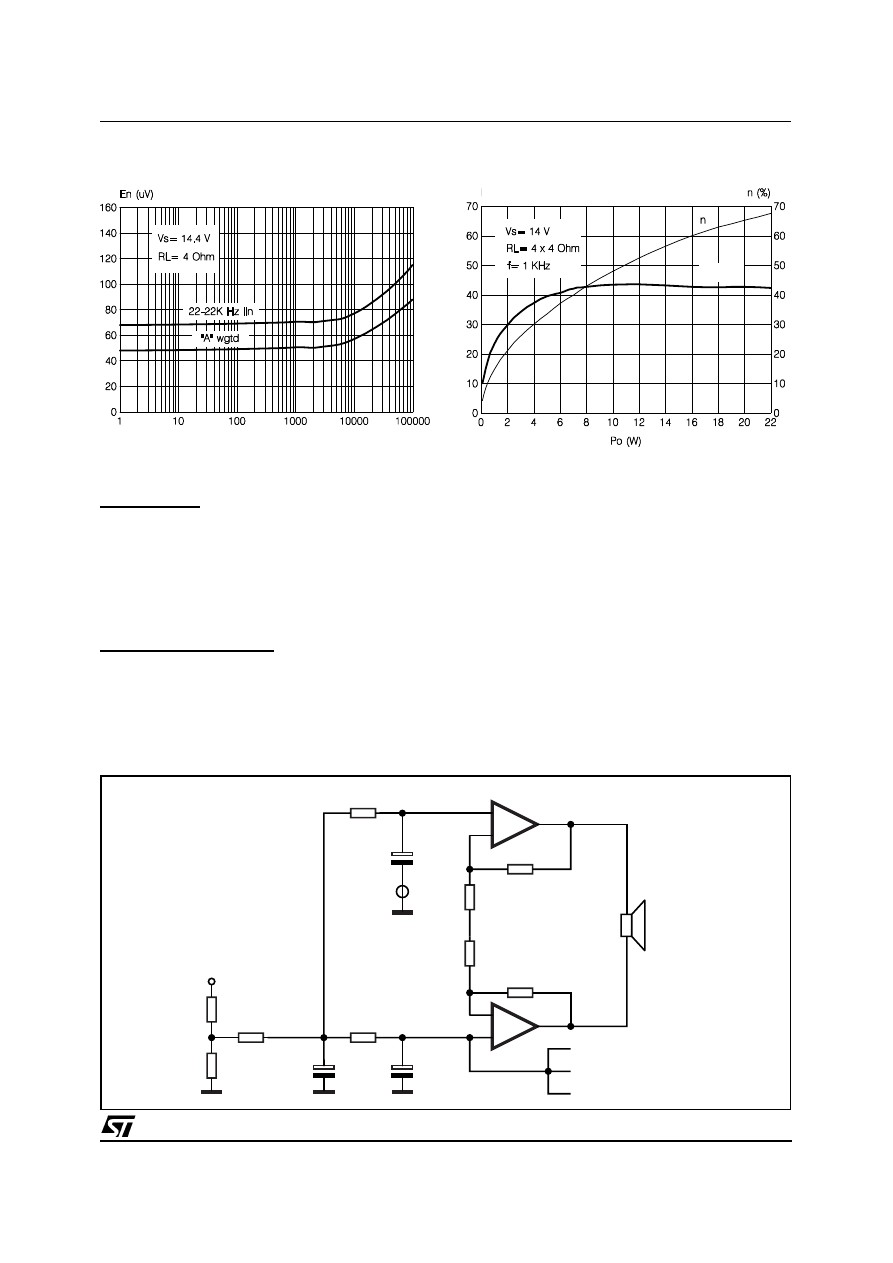
Figure 9: Output Noise vs. Source Resistance
Figure 10: Power Dissipation & Efficiency vs.
Output Power
R
g
(
Ω
)
P
tot
(W)
P
tot
INPUT STAGE
The TDA7382’S inputs are ground-compatible
and can stand very high input signals (
±
8Vpk)
without any performances degradation.
If the standard value for the input capacitors
(0.1
µ
F) is adopted, the low frequency cut-off will
amount to 16 Hz.
STAND-BY AND MUTING
STAND-BY and MUTING facilities are both
CMOS-COMPATIBLE. If unused, a straight con-
nection to Vs of their respective pins would be ad-
missible. Conventional low-power transistors can
be employed to drive muting and stand-by pins in
absence of true CMOS ports or microprocessors.
R-C cells have always to be used in order to
smooth down the transitions for preventing any
audible transient noises.
Since a DC current of about 10 uA normally flows
out of pin 22, the maximum allowable muting-se-
ries resistance (R
2
) is 70K
Ω
, which is sufficiently
high to permit a muting capacitor reasonably
small (about 1
µ
F).
If R
2
is higher than recommended, the involved
risk will be that the voltage at pin 22 may rise to
above the 1.5 V threshold voltage and the device
will consequently fail to turn OFF when the mute
line is brought down.
About the stand-by, the time constant to be as-
+
-
0.1
µ
F
C1 ÷ C4
+
-
8K
Ω
8K
Ω
400
Ω
400
Ω
100K
Ω
100K
Ω
70K
Ω
IN
D95AU302
TOWARDS
OTHER CHANNELS
10K
Ω
10K
Ω
V
S
47
µ
F
C6
0.1
µ
F
C5
SVR
AC_GND
Figure 11: Input/Output Biasing.
TDA7382
7/10
signed in order to obtain a virtually pop-free tran-
sition has to be slower than 2.5V/ms.
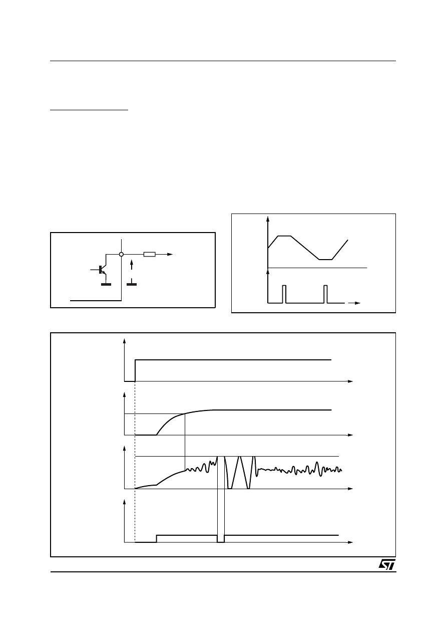
CLIPPING DETECTOR
The CLIPPING DETECTOR acts in a way to out-
put a signal as soon as one or more outputs
reach or trespass a typical THD level of 10%.
As a result, the clipping-related signal at pin 25
takes the form of pulses, which are syncronized
with each single clipping event in the music pro-
gram. Applications making use of this facility
usually operate a filtering/integration of the pulses
train through passive R-C networks and realize a
volume (or tone bass) stepping down in associa-
tion with microprocessor-driven audioprocessors.
The maximum load that pin 25 can sustain is
1K
Ω
.
Due to its operating principles, the clipping detec-
tor has to be viewed mainly as a power-depend-
ent feature rather than frequency-dependent. This
means that clipping state causing THD = 10%
typ. will be immediately signaled out whenever a
fixed power level is reached, regardless of the
audio frequency.
In other words, this feature offers the means to
counteract the extremely sound-damaging effects
of heavy clipping, caused by a sudden increase of
odd order harmonics and appearance of serious
intermodulation phenomena.
VREF
R
Vpin 25
25
D97AU810
TDA7382
Figure 12: Diagnostics circuit.
AUDIO
OUTPUT
SIGNAL
CLIPPING
DET.
OUTPUT
CURR.
time
D97AU811
V
O
ICLIP
0
Figure 13: Clipping Detection Waveforms.
t
t
t
MUTE PIN
VOLTAGE
Vs
OUTPUT
WAVEFORM
Vpin 25
WAVEFORM
D97AU812A
CLIPPING
ST-BY PIN
VOLTAGE
t
Figure 14: Diagnostics Waveforms.
TDA7382
8/10
Flexiwatt25
DIM.
mm
inch
MIN.
TYP.
MAX.
MIN.
TYP.
MAX.
A
4.45
4.50
4.65
0.175
0.177
0.183
B
1.80
1.90
2.00
0.070
0.074
0.079
C
1.40
0.055
D
0.75
0.90
1.05
0.029
0.035
0.041
E
0.37
0.39
0.42
0.014
0.015
0.016
F (1)
0.57
0.022
G
0.80
1.00
1.20
0.031
0.040
0.047
G1
23.75
24.00
24.25
0.935
0.945
0.955
H (2)
28.90
29.23
29.30
1.138
1.150
1.153
H1
17.00
0.669
H2
12.80
0.503
H3
0.80
0.031
L (2)
22.07
22.47
22.87
0.869
0.884
0.904
L1
18.57
18.97
19.37
0.731
0.747
0.762
L2 (2)
15.50
15.70
15.90
0.610
0.618
0.626
L3
7.70
7.85
7.95
0.303
0.309
0.313
L4
5
0.197
L5
3.5
0.138
M
3.70
4.00
4.30
0.145
0.157
0.169
M1
3.60
4.00
4.40
0.142
0.157
0.173
N
2.20
0.086
O
2
0.079
R
1.70
0.067
R1
0.5
0.02
R2
0.3
0.12
R3
1.25
0.049
R4
0.50
0.019
V
5˚ (Typ.)
V1
3˚ (Typ.)
V2
20˚ (Typ.)
V3
45˚ (Typ.)
(1): dam-bar protusion not included
(2): molding protusion included
H3
R4
G
V
G1
L2
H1
H
F
M1
L
FLEX25ME
V3
O
L3
L4
H2
R3
N
V2
R
R2
R2
C
B
L1
M
R1
L5
R1
R1
E
D
A
V
V1
V1
OUTLINE AND
MECHANICAL DATA
TDA7382
9/10

Information furnished is believed to be accurate and reliable. However, STMicroelectronics assumes no responsibility for the consequences
of use of such information nor for any infringement of patents or other rights of third parties which may result from its use. No license is
granted by implication or otherwise under any patent or patent rights of STMicroelectronics. Specification mentioned in this publication are
subject to change without notice. This publication supersedes and replaces all information previously supplied. STMicroelectronics products
are not authorized for use as critical components in life support devices or systems without express written approval of STMicroelectronics.
The ST logo is a registered trademark of STMicroelectronics
© 2001 STMicroelectronics – Printed in Italy – All Rights Reserved
STMicroelectronics GROUP OF COMPANIES
Australia - Brazil - Canada - China - Finland - France - Germany - Hong Kong - India - Israel - Italy - Japan - Malaysia - Malta - Morocco -
Singapore - Spain - Sweden - Switzerland - United Kingdom - United States.
http://www.st.com
TDA7382
10/10
Wyszukiwarka
Podobne podstrony:
TDA7388 STMicroelectronics elenota pl
TDA7383 STMicroelectronics elenota pl
TDA7386 STMicroelectronics elenota pl (2)
TDA7385 STMicroelectronics elenota pl
TDA7381 STMicroelectronics elenota pl
TDA7389A STMicroelectronics elenota pl
TDA7386 STMicroelectronics elenota pl (1)
TDA7566 STMicroelectronics elenota pl
TDA7266M STMicroelectronics elenota pl
TDA7850 STMicroelectronics elenota pl
TDA7490LSA STMicroelectronics elenota pl
TDA1908 STMicroelectronics elenota pl (1)
TDA7233 STMicroelectronics elenota pl
TDA7231A STMicroelectronics elenota pl
TDA7360 STMicroelectronics elenota pl
TDA7490SA STMicroelectronics elenota pl
TDA7370B STMicroelectronics elenota pl
TDA2007A STMicroelectronics elenota pl
więcej podobnych podstron