
Agenda
A. Can not power on
B. “Insert SIM”
C. Display abnormal
D. No Keypad’s and LCM backlight
E. Receiver no key tone
F. No ring tone
G. Can not charge
H. Keypad no function
I. Vibrator out of control
J. Microphone no function
K. Earphone no function
L. RTC ab-normal
M. Phone hang
N. Auto power on
O. Auto power off
P. Can not call out
Q.FM no function (only available
for W213)
A. Can’t power on
1. Check the voltage of the battery.
VBAT (
red square
)>3.6V
2. Check Battery connector J703
Probe Point
Battery connector
Should be >3.6V
A. Can’t power on
3. Check the Power-ON path.
Power on path
R802/D801
2
1
D801
1PS79SB30
C805
33pF
R806
1K
R802
1K
(POWER/ END)
KBR4
DGND
1
2
S802
DGND
RPWON
A. Can’t power on
4. CheckTriton_lite regulator voltage.
A.
VRABB_2.8V should be 2.8V(C147)
B.
VRIO_1.8V should be 1.8V(C155)
C.
VRMEM_1.8V should be 1.8V(C141)
Probe Point
C141
C147
C155
Triton lite

A. Can’t power on
5. Try to download SW to the damaged unit. If the damaged unit can not
power on, you can check the Flash Memory IC(U301) , LOCOSTO(U101) and
Triton_lite (U103).
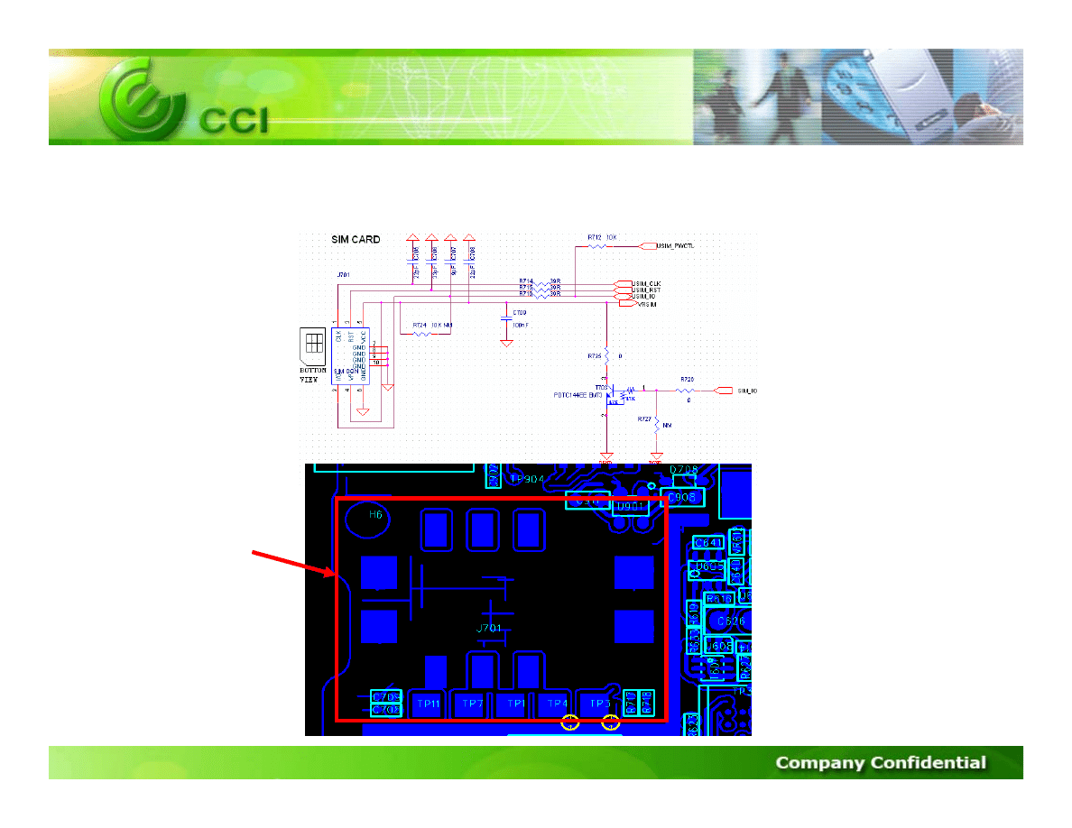
B. “Insert SIM” issue
1. Download SW to the damaged unit
2. Check the SIM connect
SIM circuit
3. Check the SIM interface between LOCOSTO(U101) & Triton_lite
(U103). under power-on routine
4. If all the signals of Triton_lite(U103) are normal and all the signals of
LOCOSTO(U101) are abnormal, please check LOCOSTO(U101).
5. If all the signals of Triton_lit(U103) are abnormal, please check
Triton_lite(U103)
B. “Insert SIM” issue
USIM_CLK
USIM_RST
USIM_IO
1. Please download SW to the damaged unit.
2. Please check the status of LCM connect.
3. Please check the LCM whether LCM is normal or damaged.
4. If LCM is normal, please check MB whether is damaged or not.
5. Please check all the signal traces of LOCOSTO (U101).
and LCD connecter.
C. No Display or Display abnormal
LCD connecter
C. No Display or Display abnormal
The following is layout of LCM connecter
Should be about VR2V8
(2.8V)
Should be VRIO (1.8V)
D. No Keypad backlight
1. Check the status of all the LEDs
2. Check the related circuits
Should be the same as VBAT (3.6-4.2V)
Probe Point
Keypad&LCM
backlight
LED

D. No LCM backlight
1. Please download SW to the damaged unit.
2. Replace the new LCM

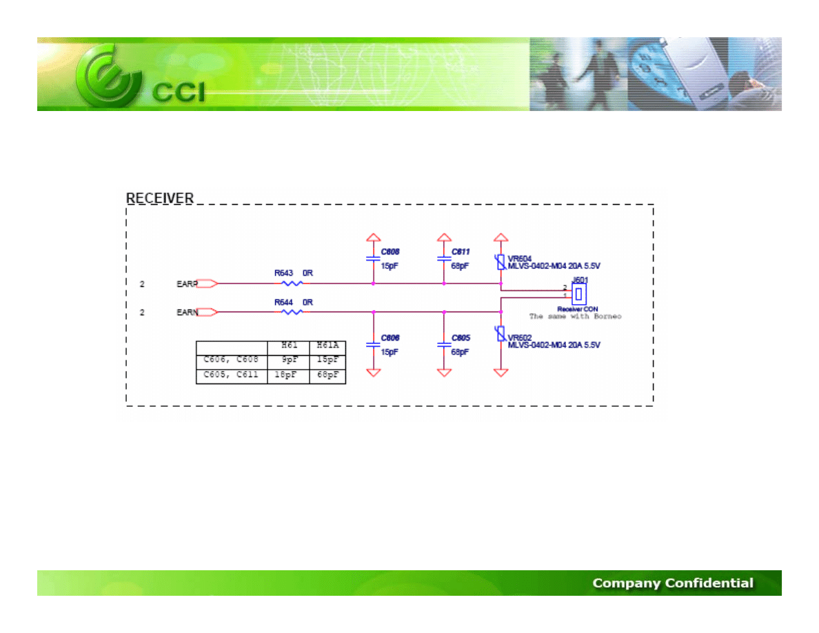
E. Receiver no key tone
1. Please download SW to the damaged unit.
2. Measure the receiver’s impedance(about 32 ohm)
3. Check whether the receiver is normal or not. If abnormal, please exchange
with the normal one and check if the function is OK now?
4. If receiver is normal, please replace with the other normal one and check
whether the function is normal or not? If the function is normal, it may be
the solder problem.
5. If MB is damaged, please check the related circuits.
6. Check the components’ connection and impedance(BL601).
5. If all the signals are abnormal, please check Triton_lite(103)
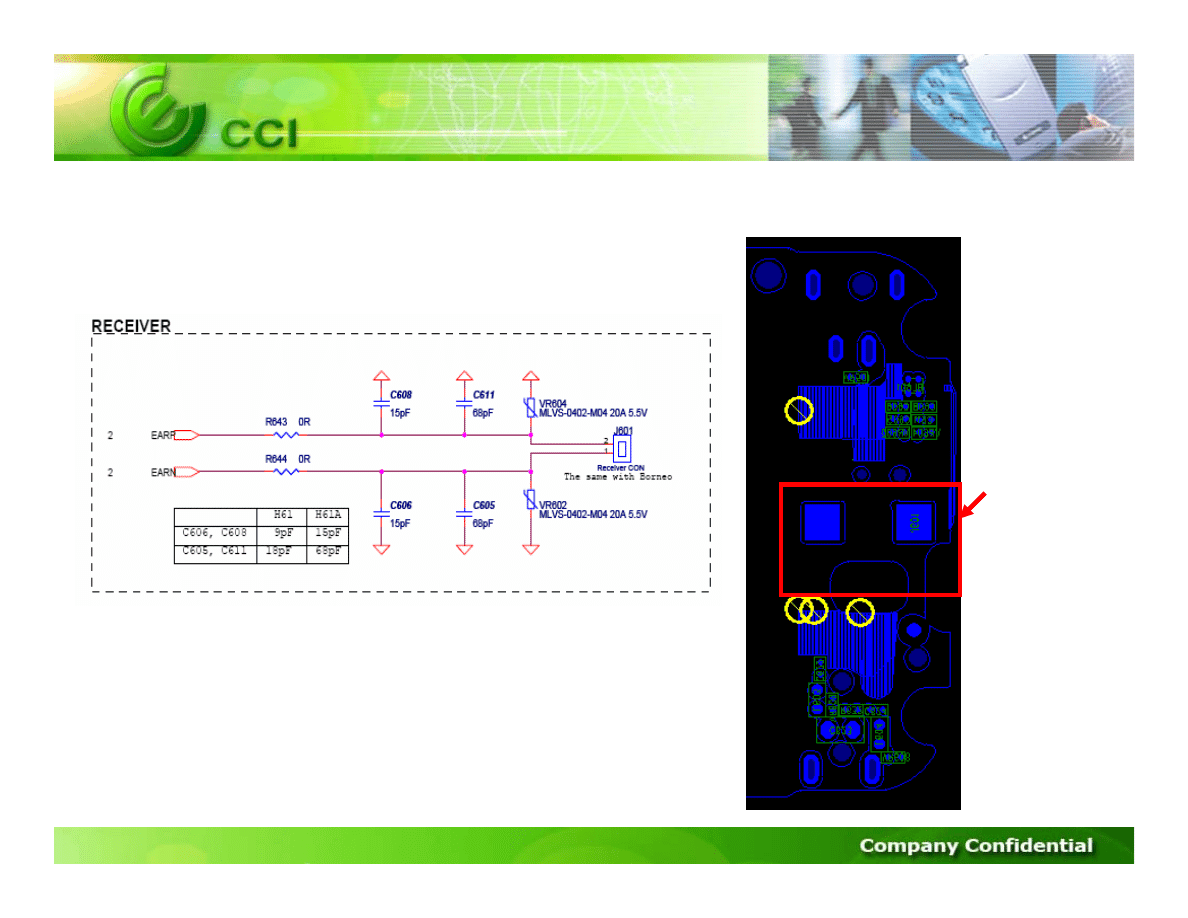
E. Receiver no key tone
Check the related circuits
Receiver
J601

F. No ring tone
1. Check the Ring volume setting.
2. Please download SW to the damaged unit.
3. Check the Speaker’s impedance(about 8ohm).
4. Check the related circuits and components include
Speaker
connecter and
Check the SPKP/SPKN of Triton_lite(U103), Vo+, Vo- & VBAT of U601.
5. If all the signals of
Speaker
are abnormal, please check Triton_lite(U103) & U601
6. If all the signals of Triton_lite(U103) & U601 are normal and all the signals of
Speaker
are abnormal, please check
Speaker
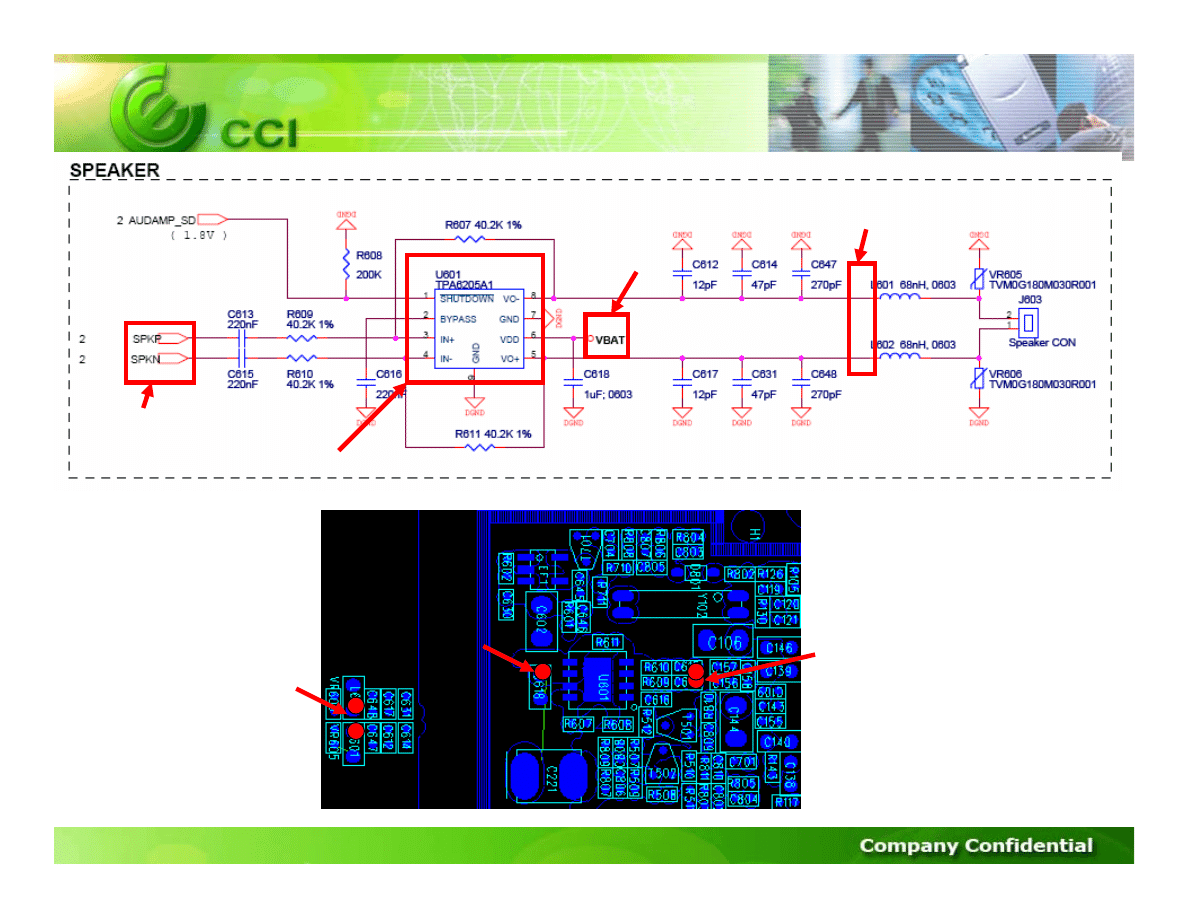
F. No ring tone
The schematic and layout of speaker and U601.
SPKP,SPKN
from U103
Vo+,Vo-
U601
VBAT
Vo+,Vo-
VBAT of U601
SPKP, SPKN
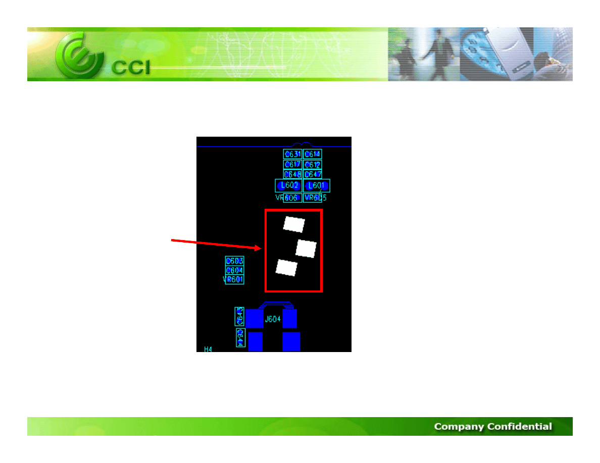
F. No ring tone
The layout of speaker
J603
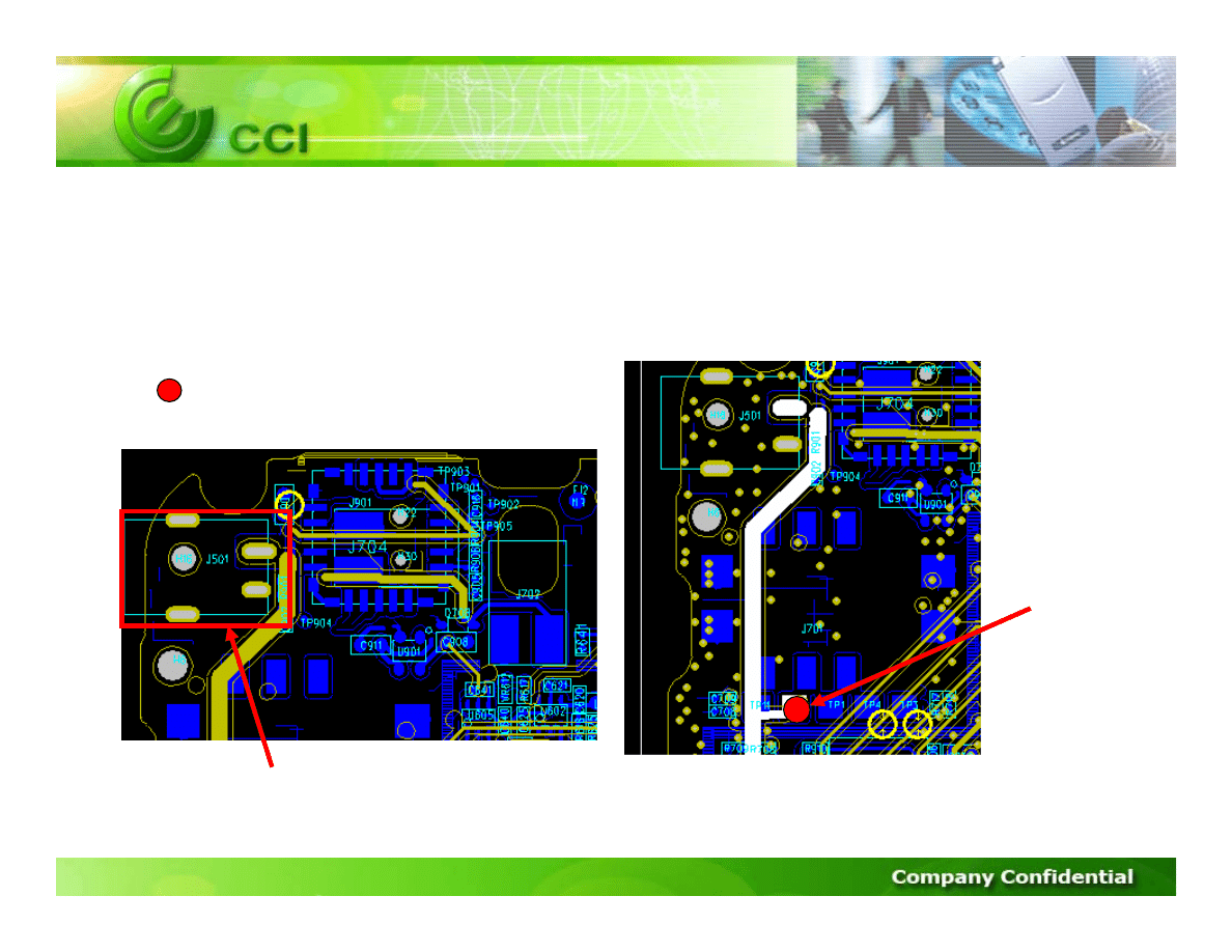
G. Can not charge
1. Check the battery and adaptor
2. Download SW to the unit.
3. Check the DC Jack(J501).
Probe Point
Charging voltage
should be 5~6V
TP7
DC Jack
G. Can not charge
4. Check the battery connect
.
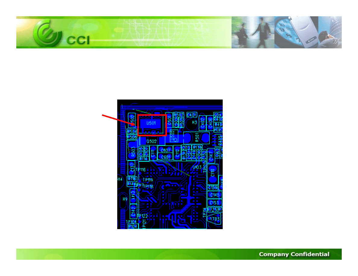
5. Check the Protect IC(U501).
U501
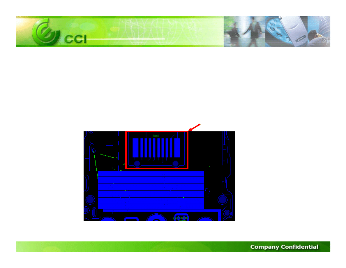
H. Keypad no function
1. Download SW to the damaged unit
2. Check the metal Done and Key.
3. If there are more than 2 Keys failed, please check the LOCOSTO(U101).
Or check the Key PAD of the PCB.
Metal Done & Key
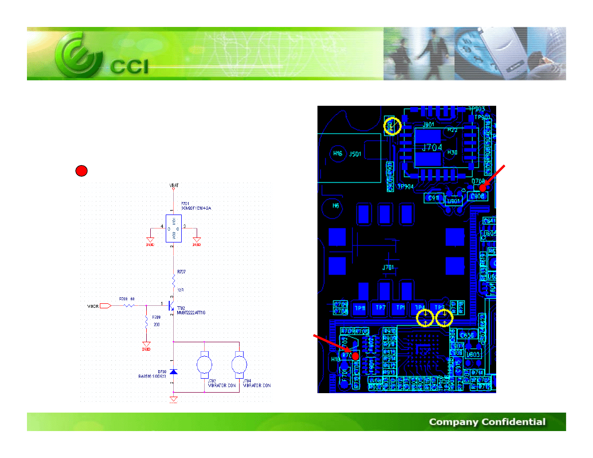
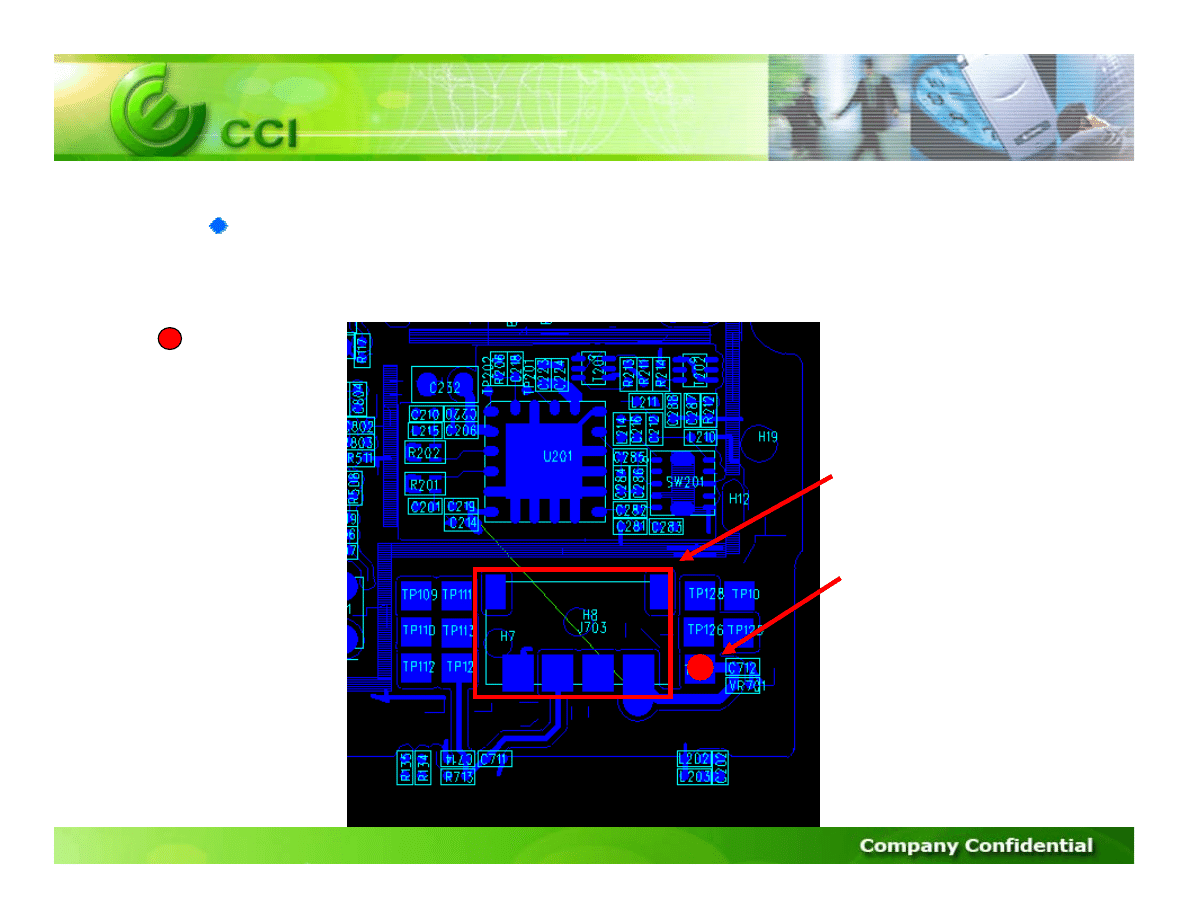
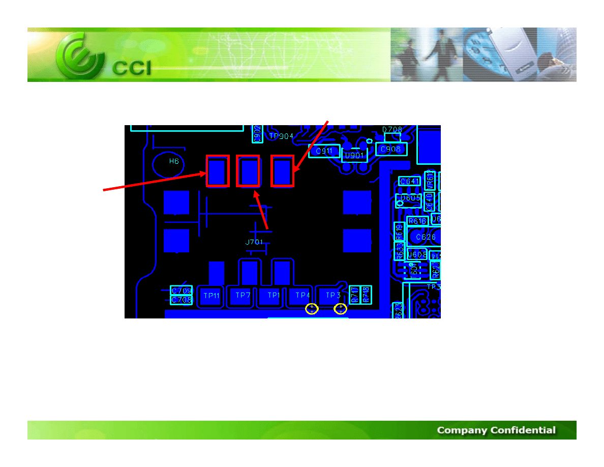
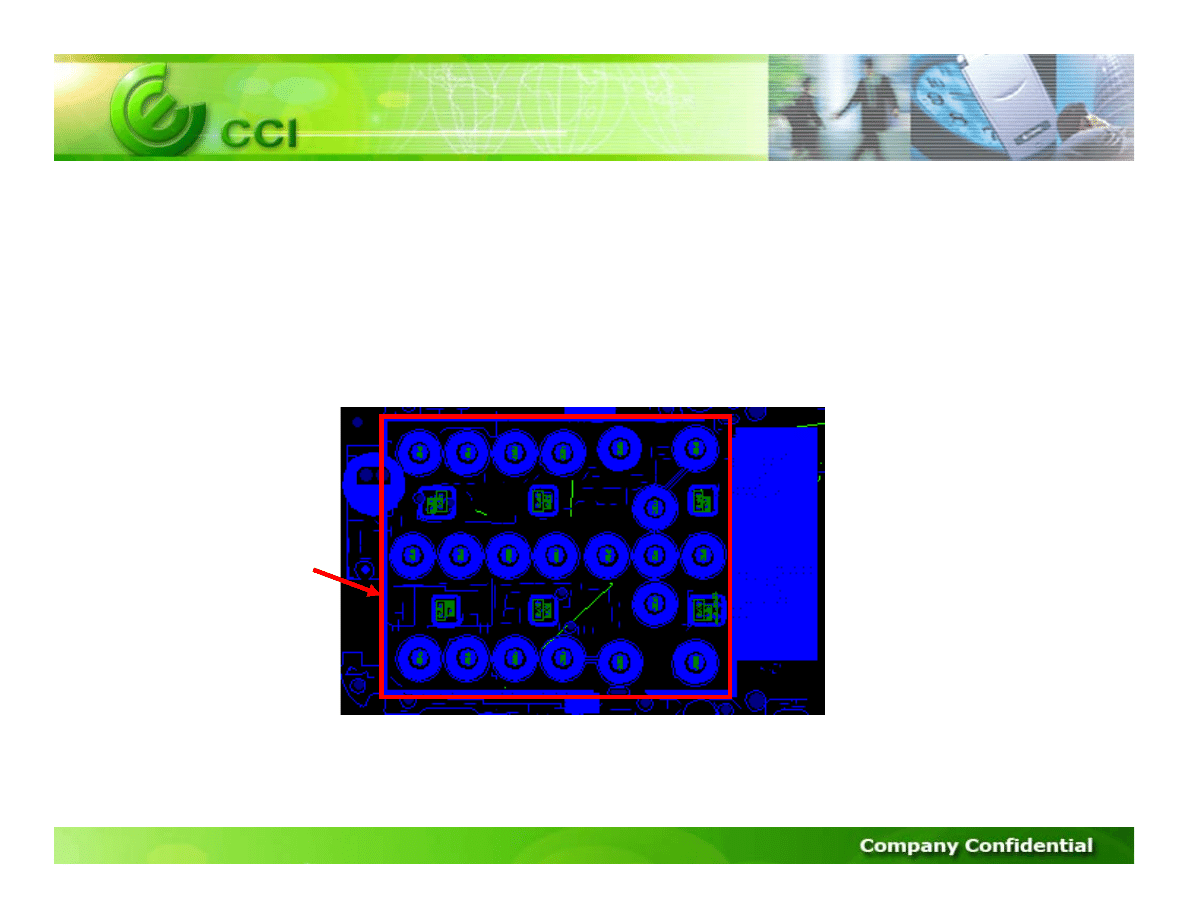
I. Vibrator abnormal
1. Check the vibration setting.
2. Check the vibrator
3. Check the related circuits
Probe Point
D708 should
be about 1.4V
R707
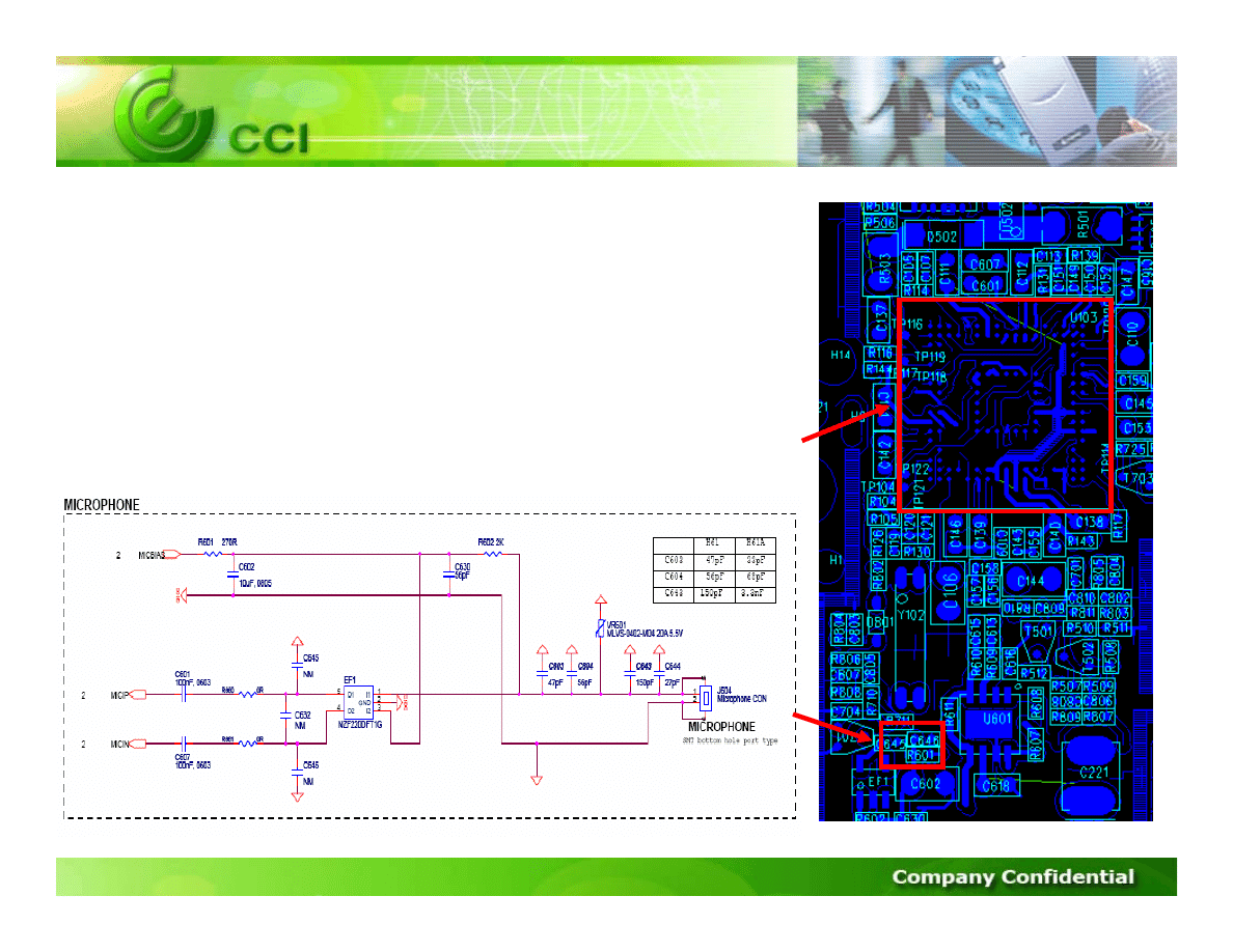
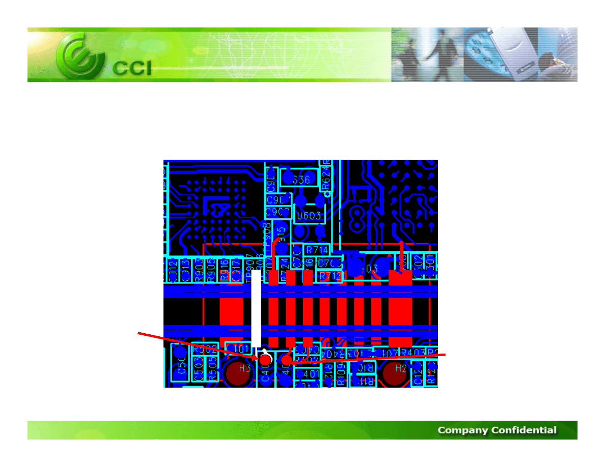
J. Microphone no function
1. Download SW to the damaged unit
2. Check or replace the microphone
3. Check the related circuits
a. If all the signals of microphone are abnormal, please check Triton_lite(U103)
b. If all the signals of Triton_lite(U103) are normal and all the signals
of microphone are abnormal, please check microphone.
c. Check other components
MIC circuit
Triton_lite
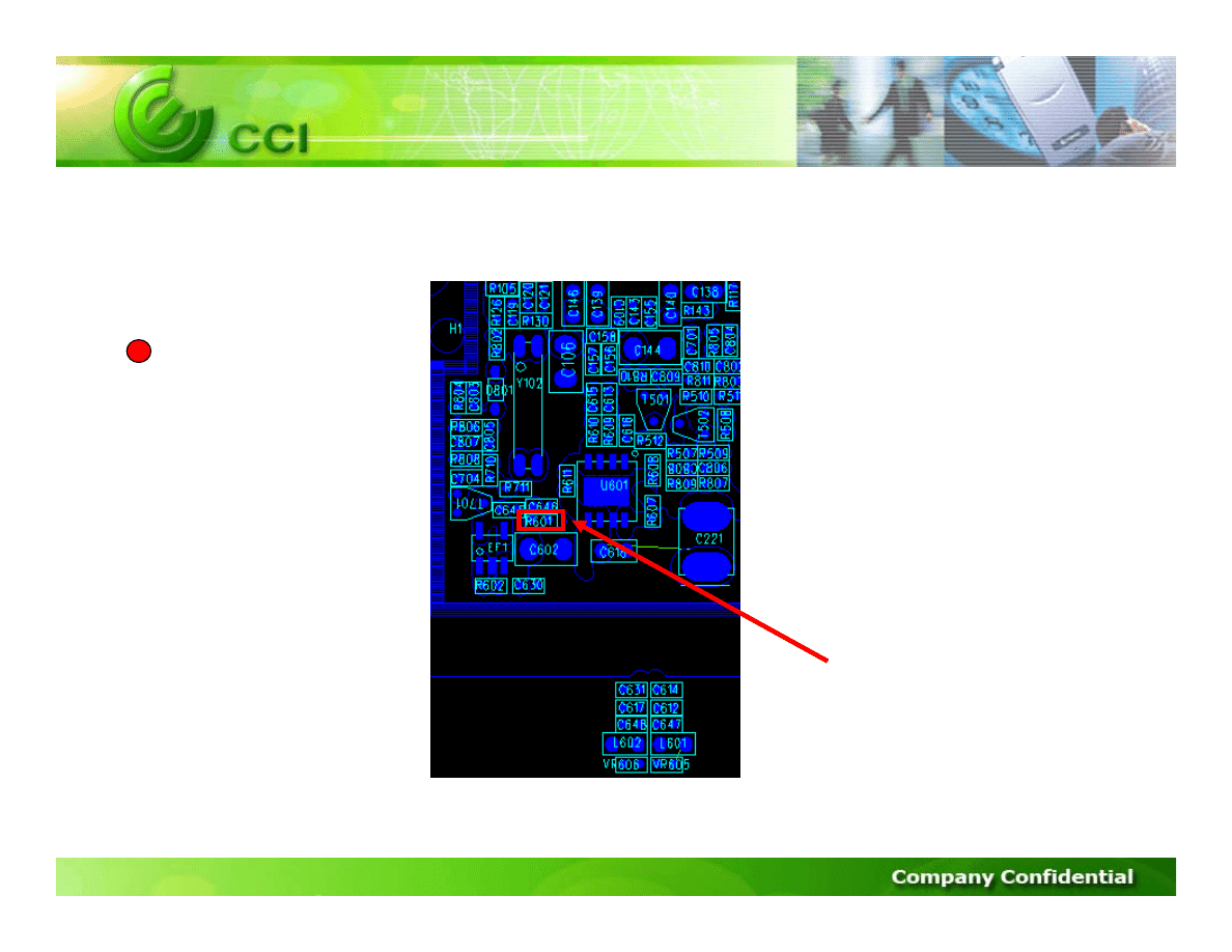
J. Microphone no function
4. Check the related circuits
Probe Point
R601
Should be about 2V
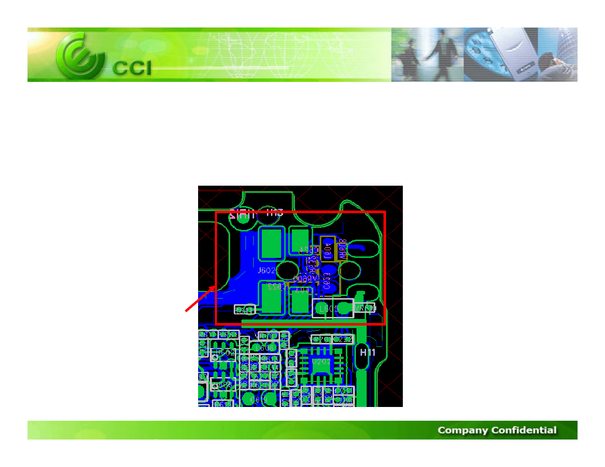
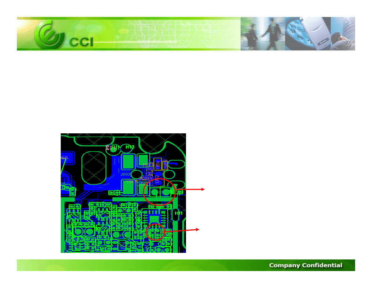
K. Earphone no function
1. Check the Earphone
2. Download SW to the damaged unit.
3. Check the Audio Jack(J602)
J602
Audio Jack
K. Earphone no function
4. Check the related circuits
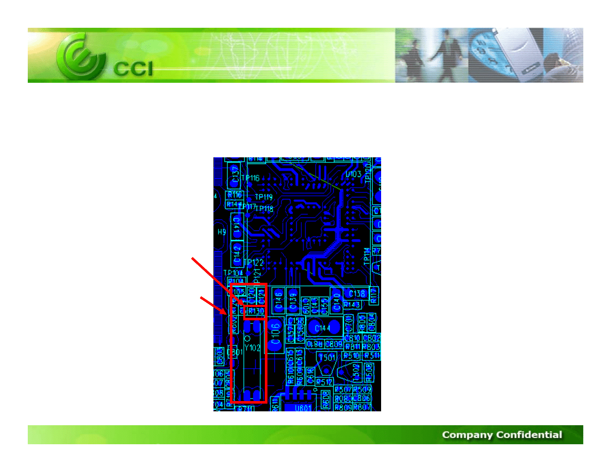
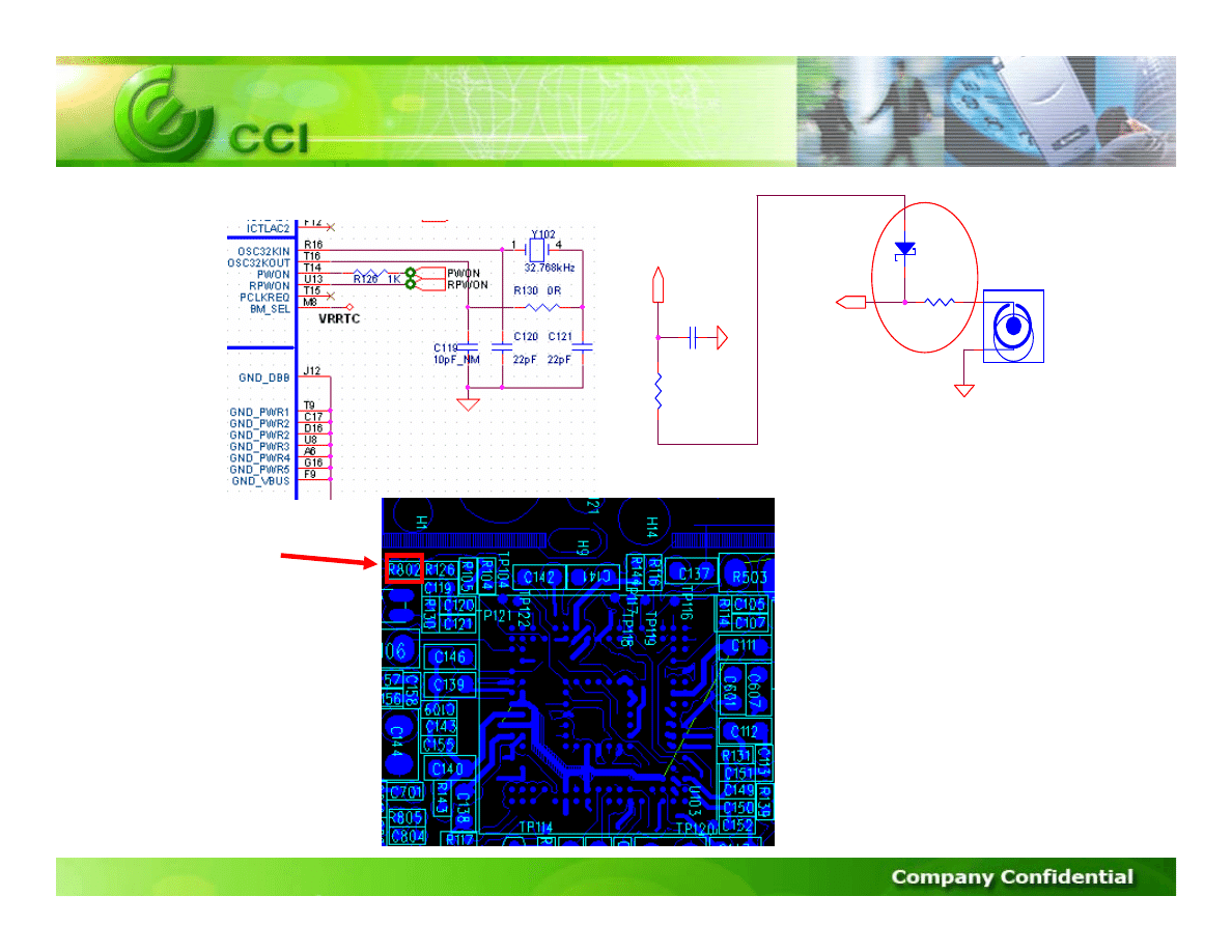
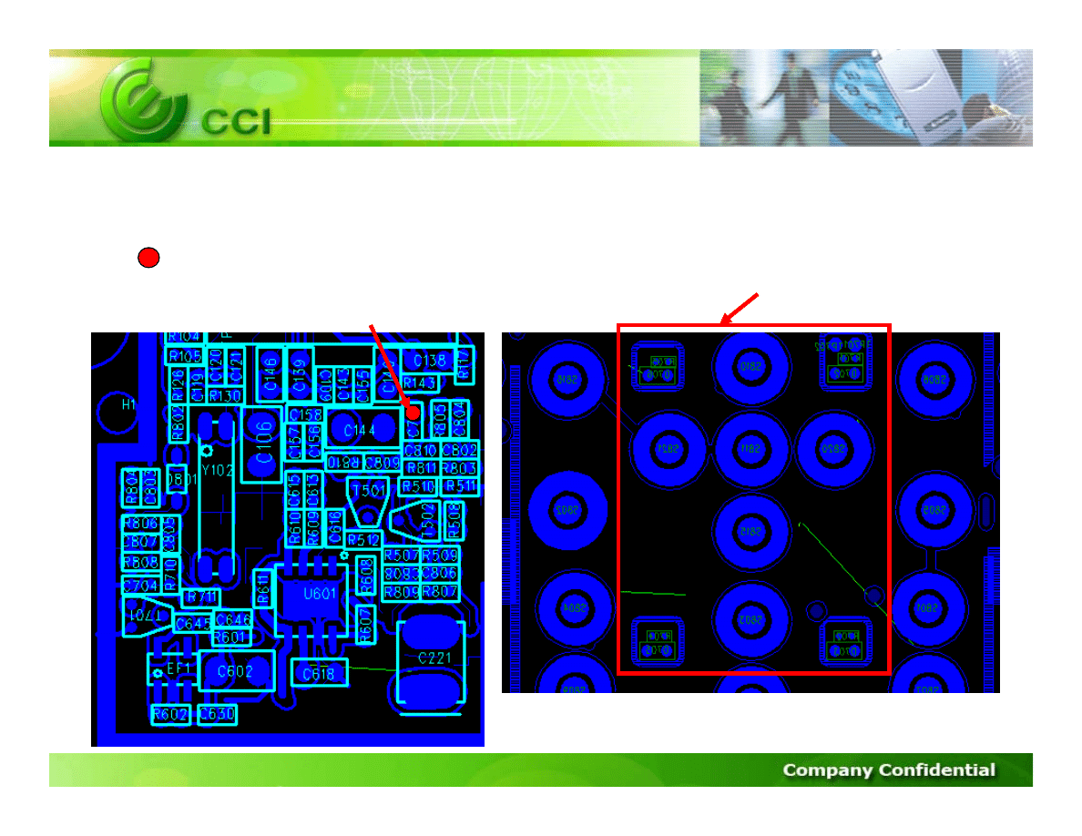
L. RTC failed
1. Download SW to the damaged unit
2. Check if the signal @ R130 is 32.768K of 32KHz oscillator
3. Check the related circuits of Triton_lite(U103)
RTC circuit
R130

M. Phone Hang
1. Try to load code from the damaged unit and download SW to the damaged
unit.
2. If the damaged unit still has the issue, check the intel flash(U301) o
r
Triton_lite(U103), LOCOSTO(U101)
N. Auto Power On
1. Please check the alarm setting of auto power on
2. Please check the power-on path(page3 A.3)
3. Please check the charger path, refer page17
4. Try to load code from the damaged unit and download SW to the damaged
unit.
If the damaged unit still has the same issue, you can check the intel
flash(U301) Or Triton_lite(U103), and LOCOSTO (U101)

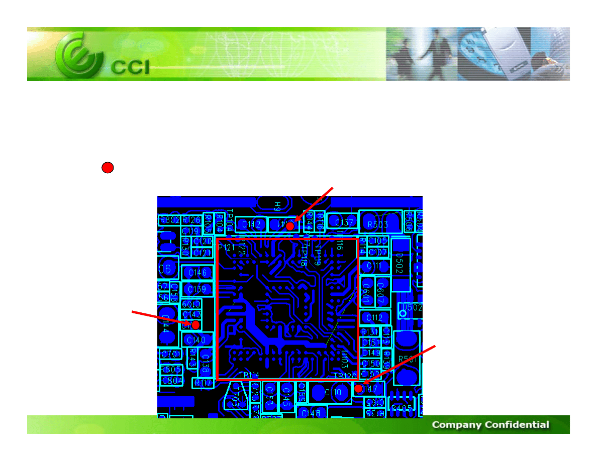
O. Auto Power Off
1. Please check the alarm setting of auto power off
2. Download SW to the damaged unit.
3. Check the leakage current (<200uA)
4. If the leakage current is normal, please Triton_lite(U103)
5. If the leakage current is abnormal, please check the part, PA(U201) & Audio
Amp(U601).
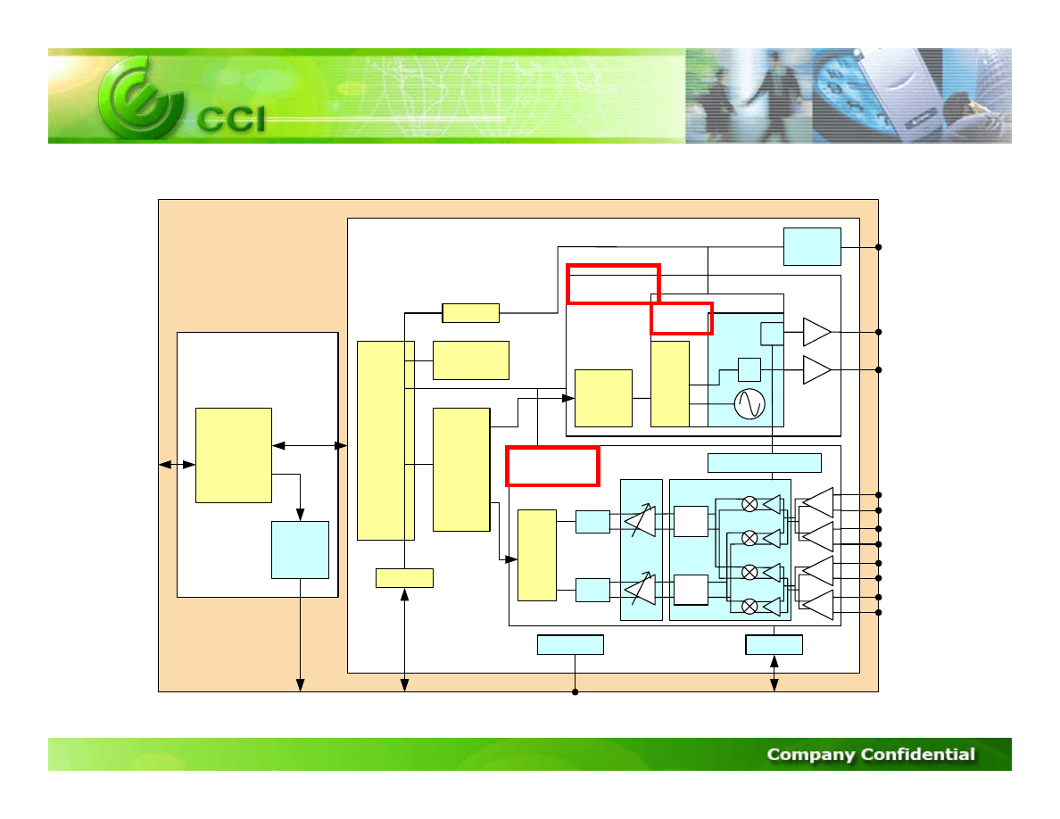
P. Can’t call out
RF Tranceiver Block Diagram
Tx LB
Tx HB
Transmitter
SC-
FILT
SC-
FILT
LNA
LNA
LNA
LNA
TA/MIX
MTDSM
CTA
ADC
ADC
DRX
DCU/PCU
Receiver
ATST
SRM
(scripts -
Rx/Tx
buffers)
OCP
DTST
BG/LDO
Script
Processor
DCXO
CKM
DRP2.0
Wrapper
Digital
Interface
to DBB
APC/
DAC
Locosto Radio
Interface
DTX
(GMSK
modulator)
%2
ADPLL
%2
ALO
DLO
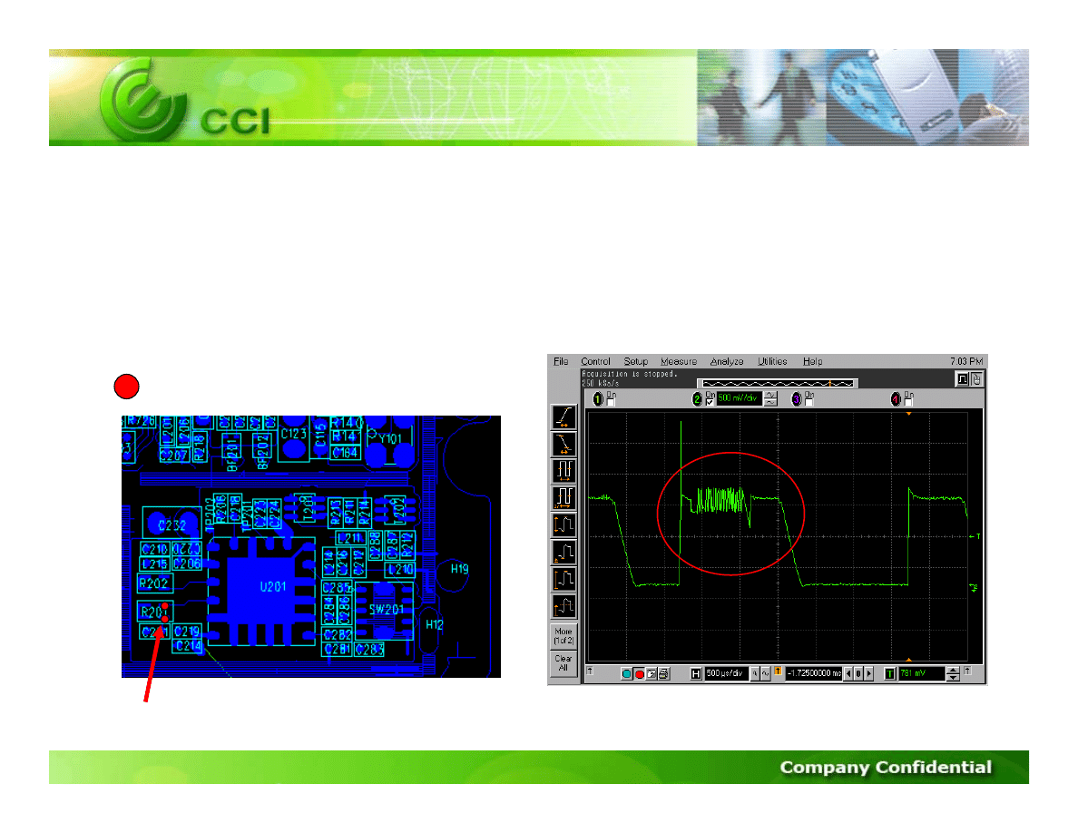
P. Can’t call out
Tx Path (I/Q) in GSM Band
1.Set HP8960 or HP8922,Operating mode:Test mode,Test function:BCH+TCH
CH62:902.4MHz, cell power:-60dBm, MS_TX_level : 5
3. Use oscilloscope probe to touch
red point
and you can find that(For
Example:The TXIP signal)
Probe Point
R201(PIN1,2)
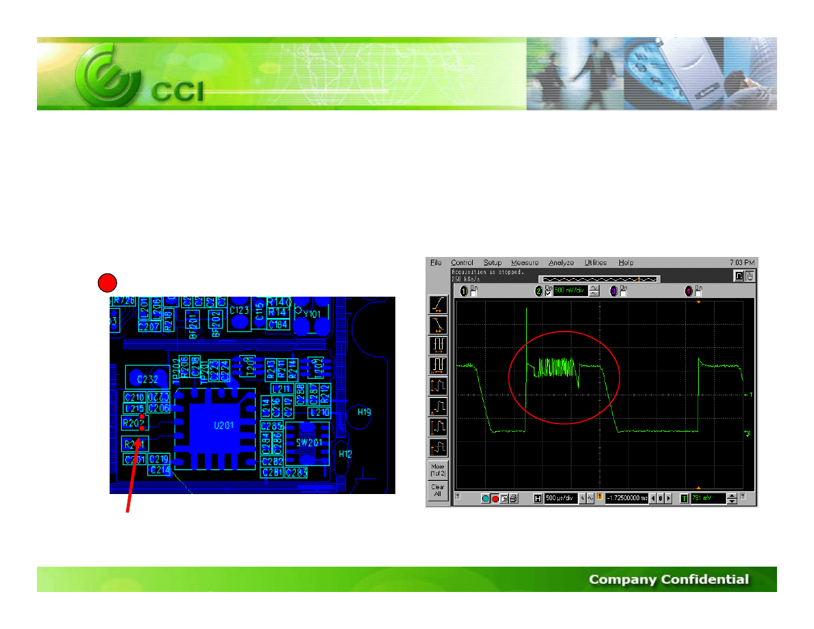
P. Can’t call out
Tx Path (I/Q) in DCS Band
1.Set HP8960 or HP8922,Operating mode:Test mode,Test function:BCH+TCH
CH699:1747.6MHz, cell power:-60dBm, MS_TX_level : 0
3.Use oscilloscope probe to touch
red point
and you can find wave(For
Example:The TXIP signal)
Probe Point
R202(PIN1,2)
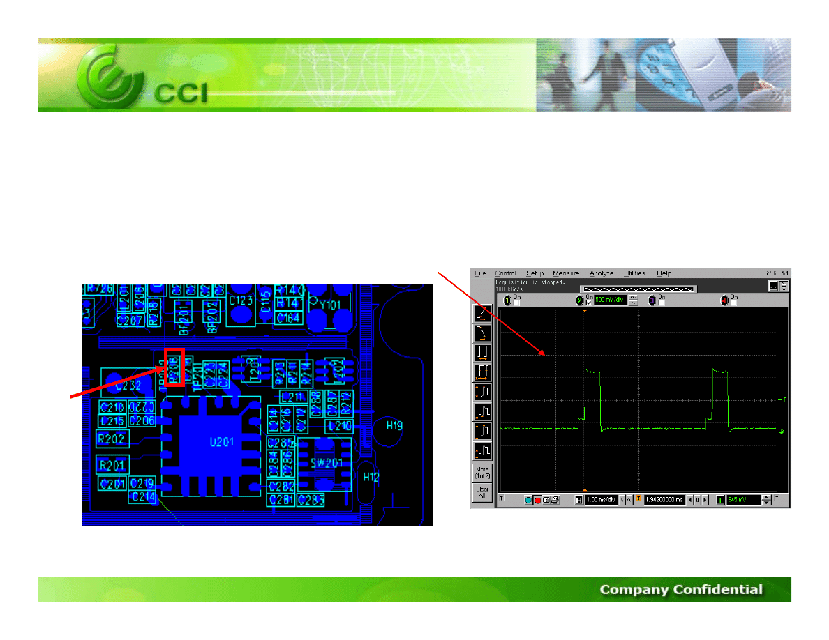
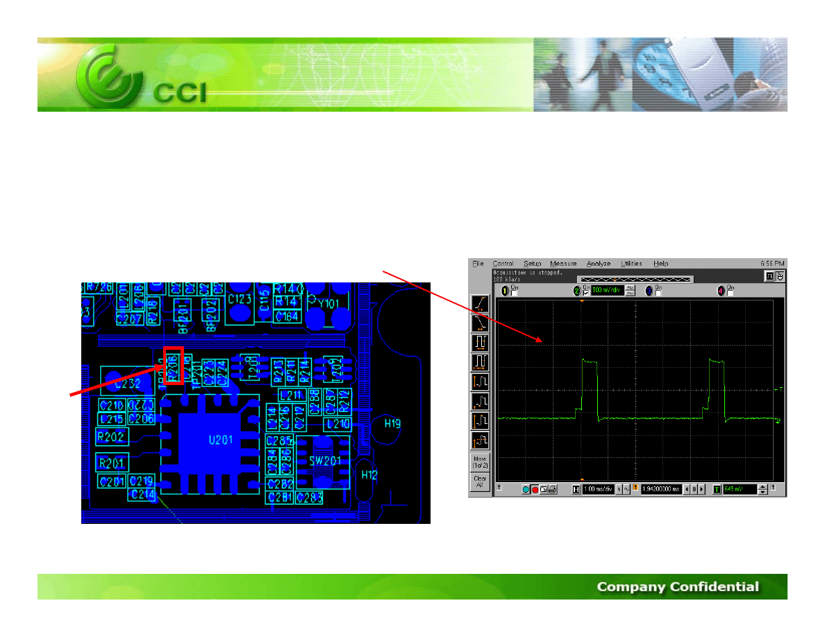
P. Can’t call out
Tx path(PA) in GSM Band
1.Set HP8960 or HP8922,Operating mode:Test mode,Test function:BCH+TCH
CH62:902.4MHz, cell power:-60dBm, MS_TX_level:5
2.TX signal1 : Use oscilloscope probe to touch R206 to get signal1 wave
Signal1(APC Wave)
R206
P. Can’t call out
Tx path(PA) in DCS Band
1.Set HP8960 or HP8922,Operating mode:Test mode,Test function:BCH+TCH
CH699:1747.6MHz, cell power:-60dBm, MS_TX_level : 0
2.TX signal1 : Use oscilloscope probe to touch R206 to get signal1 wave
signal1
R206
P. Can’t call out
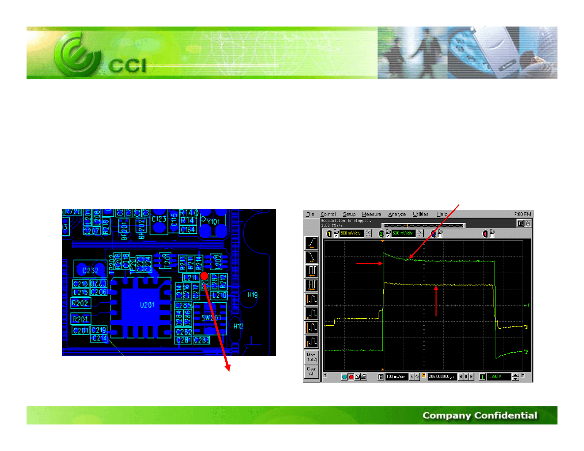
Tx path(TR switch) in GSM Band
1.Set HP8960 or HP8922,Operating mode:Test mode,Test function:BCH+TCH
CH62:902.4MHz, cell power:-60dBm, MS_TX_level : 5
2.TX signal1 : Use oscilloscope probe to touch SW201 Pin10(C287) to get signal1 wave
Signal1
VC_LB
APC
C287
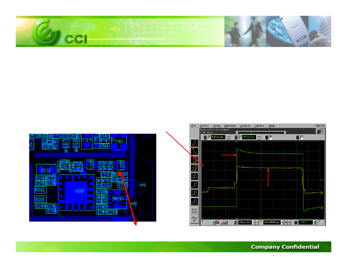
P. Can’t call out
Tx path(TR switch) in DCS Band
1.Set HP8960 or HP8922,Operating mode:Test mode,Test function:BCH+TCH
CH699:1747.6MHz, cell power:-60dBm, MS_TX_level : 0
2.TX signal1 : Use oscilloscope probe to touch SW201 Pin2(C288) to get signal1 wave
Signal1
VC_HB
APC
C288
Q. FM no function (only available for W213)
1.Please Check if the Headphone connected well( Headphone antenna is used )
2.Download SW to the damaged unit.
3.Please Check the output of FM IC(U202) . (Replace FM IC if there is no/bad
signal at output of FM IC)
4.Please Check Triton_lite(U103)
Headphone antenna path
Output of FM IC
Document Outline
Wyszukiwarka
Podobne podstrony:
BD W206 W213 A3 C L3 V1
TS V180 A4 L3 V1[1] 2
TS Triplets Refresh A4 C L3 V1[1] 1
CD P7689 A4 C L3 V1 0
PL V180 8486962P01 P3 A4 C L3 V1[1] 1
Circuit Description W510 A4 C L3 v1 Description
BDSD TriplestR A4 C L3 V1[1] 0
SchRF T191 1900 C A4 L3 V1 0
PL V150 8403547B02 P3B 1 A4 C L3 V1[1] 0
SP DCSST85 A4 C L3 V1 0
BL T191 1900 BW A4 L3 V1 0
Parts List V300 500 600 P5 1 A4 C L3 V1 0
Parts List V3x A4 BW L3 V1 1
PL V3 8488386N06 B A4 BW L3 V1[1] 1
Parts List V3 05 A4 BW L3 V1(1) 0
Parts List W220 A4 BW L3 V1 0
Parts List V3 05 A4 BW L3 V1 0
PL Z3 A4 BW L3 V1 0
więcej podobnych podstron