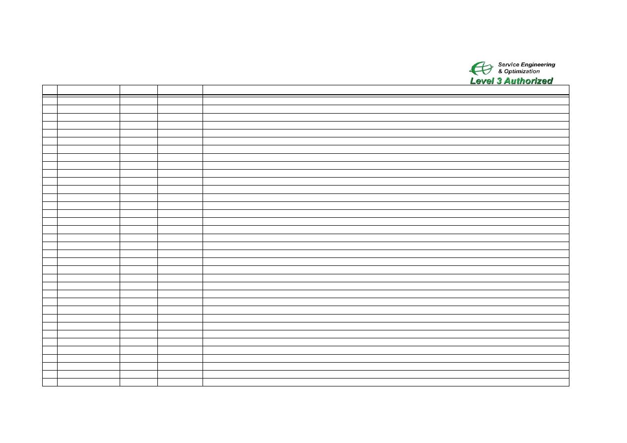
Triplets Refresh Block Diagram Signal Description
Signal
From
To
Description
1
ADDRESS(24)
U800
U701
Multipexer input to select Memory Partition 1 or 2 of Flash Memory
2
AD_TRIG
EXC_EN
U900
Transmitt Mode indication to Pcap to adjust the Battery Meter between RX Idle Mode and Transmitt Mode
3
AD6
BATT_FDBK
U900
Analog input to measure the Pull Down Resistor in the Charge accessory. Indicates the type of charger to the Phone
4
ADC DATA
Q801
U800
A
nalog voltage
D
etect input to the Sense input of Neptune to indicate the Status of the Light sensor Q801
5
ALERT-
U900
Alert
ALERT
Out Negatve (
-
) from Alert amplifier to Alert speaker
6
ALERT+
U900
Alert
ALERT
Out Positive (
+
)from Alert amplifier to Alert speaker
7
ANTENNA
U301 R906
ANTENNA
Transmitt/ Receive signlal from/ to Bluetooth Chip
8
AOC_DRIVE
U800
U300
Bias control signal to U300 TX amplifier (
A
utomatic
O
utput
C
ontrol
D
river)
9
ATI1.8V
U900
J1300
Orginal
VBUCK
to supply the ATI Display driver IC
10
AUD_REG
U900
U900
AUD
io
2,775V
support voltage for U900 internal functions
11
AUDIO_IN
J1400
U900
Analog Audio Input from Accesory to Pcap Audio Interface.
12
AUDIO_OUT
U900
J1400
Analog Audio Output from Pcap Audio Interface to support Accesory.
13
B+
U900
U900
Main Source for the Phone supporting U900 power supply
14
BATT_DETB
U900
U800
BATT
ery
In/output detection to Sim Interface of U800. Renamed and used as SIM_PD at U800
15
BATT_DETB
U900
U800
BATT
ery
DET
ection indication from PCap to U800 SIM Interface to force the VSIM_EN output of U800
16
BATT_FDBK
U900
FL1400 - J1400
BATT
erie
F
ee
DB
ac
K
Line to adjust the External Power Supplys to 1,4 Volt above Batterie Voltage Level
17
BATT+
M1700
Q952, U900
BATT
ery (
+
) output/input to Battery switch and U900 AD converter input
18
BB_I
U150
U800
positive
I
n phase baseband signal from receiver in Algae to A/D converter in Netune
19
BB_IX
U150
U800
negative
I
n phase baseband signal from receiver in Algae to A/D converter in Netune
20
BB_Q
U150
U800
positive
Q
uadratur-phase signal from receiver in Algae to A/D converter in Netune
21
BB_QX
U150
U800
negative
Q
uadratur-phase signal from receiver in Algae to A/D converter in Netune
22
BB_SAP_CLK
U800
U301, U900
B
ase
B
and
S
erial
A
udio
P
ort
CL
oc
K
to Clock Audio Data Flow (Audio SPI Bus)
23
BB_SAP_FS
U800
U301, U900
B
ase
B
and
S
erial
A
udio
P
ort
F
rame
S
ynchronisation to syncronize the Audio Frames (Audio SPI Bus)
24
BB_SAP_RX
U301, U900
U800
B
ase
B
and
S
erial
A
udio
P
ort
R
eceive signal to U800 (Audio SPI Bus)
25
BB_SAP_TX
U800
U301, U900
B
ase
B
and
S
erial
A
udio
P
ort
T
ransmitt
signal to U900 and U301 (Audio SPI Bus)
26
BB_SPI_CLK
U800
U900
B
ase
B
and
SPI
Bus
CL
oc
K
to Clock Data Flow (Neptune /PCAP Control Communication)
27
BB_SPI_MISO
U900
U800
B
ase
B
and
SPI
Bus
M
aster (U800)
I
nput, Slave (U900)
O
utput (Neptune /PCAP Control Communication)
28
BB_SPI_MOSI
U800
U900
B
ase
B
and
SPI
Bus
M
aster (U800)
O
utput,
S
lave (U900)
I
nput (Neptune /PCAP Control Communication)
29
BL_FB
U900
R1459
FeedBack control signal to BL_SINK. R1459 will set the BL_SINK input current.
30
BL_SINK
Backlight LED
U900
SINK input to Pcap to control the LED current and on/Off function
31
BLUE_CLK_ENB
U900
U301
Orginal
CLK
_32KHz from Pcap as Enable indication to the Bluetooth Chip
32
BLUE_CTS
U800
U301
C
lear
T
o
S
end Data indication from U800 To U301 ( InterChip Communication)
33
BLUE_HOST_WAKEB
U301
U800
Communication
WAKE
up signal from U301 to U800
34
BLUE_RESETB
U900
U301
Orginal
RESETB
from U900 to reset the Bluetooth Chip
35
BLUE_RTS
U301
U800
R
equest
T
o
S
end Indication from U301 to U800 Page 1of 5
36
BLUE_RX
U301
U800
R
eceive Data Communication from U301 to U800 ( InterChip Communication)

37
BLUE_TX
U800
U301
T
ransmitt Data Communication from U800 To U301( InterChip Communication)
38
BLUE_WAKEB
U800
U301
Communication
WAKE
up signal from U800 to U301
39
BTRF_REG
U900
U301
1,8 Volt regulator output from Pcap to support the
BT
Chipset U301
40
BURSTCLK
U800
U701
BURST
CL
oc
K
to clock U700 to syncronize the loading of addresses and delivery of burst read data
41
CE_1
U701
U700
Flash Memory chip select for Memory Partition 1 of the Flash IC U700
42
CE_2
U701
U700
Flash Memory chip select for Memory Partition 1 of the Flash IC U700
43
CHRGC
U900
Q950
Analog Tuning Voltage to drive /control the current flow of the Charge Transistor Q950 into the Battery
44
CLK_32KHZ
U900
U800, U1301
32KHZ
CL
oc
K
output to RTC timer interface in Neptune and J1300
45
CLK_32KHZ_B
U1301
J1300
B
uffered
32Khz CL
oc
K
to support the Camera Driver with system Clock
46
CLK-13MHZ
U800
U900
13 MHz
Core
CL
oc
K
to PCap
47
CM_IN
U150
U800
Decoupled Ground Connection for RX BaseBand signals
48
CS0B
U800
U701
C
hip
S
elect
0
- active low output is used as external Flash Memory chip select
49
CTS2
U800
U301
C
lear
T
o
S
end Data indication from U800 To U301 ( InterChip Communication)
50
D-
U900/ J1400
J1400/ U900
USB
D
ata
-
line in/output passing the FL1400 ESD protection Fliter
51
D+
U900/ J1400
J1400/ U900
USB
D
ata
+
line in/output passing the FL1400 ESD protection Fliter
52
DSEL0
J1400
U800
This pin is used to select between serveral different
D
umb type devices ( External Audio devices like MP3Player, FM Radio...)
53
DSEL1
J1400
U800
This pin is used to select between serveral different
D
umb type devices ( External Audio devices like MP3Player, FM Radio...)
54
DSEL2
J1400
U800
This pin is used to select between serveral different
D
umb type devices ( External Audio devices like MP3Player, FM Radio...)
55
EB0_B
U800
U700
Used as write
E
nable to partition of SRAM
56
EB1_B
U800
U700
Used as write
E
nable to partition of SRAM
57
ECBB
U800
U700
E
nd
O
ff
C
urret
B
urst-active low(
B
)- to indicate to FLASH the end of current burst sequence.
58
EURO_US
U800
U50
Band Selection Signal from Neptune to RX/TX Switch in Eagle IC U50
59
EXC_EN
U800
U50, U150
EXC
iter
EN
able
active high to drive the Switch Control Circuit to TX mode and TX indication to Eagle IC
60
EXT_B+
Q954
Q953, U900
Over Voltage controlled
RAW_EXT_B+
as Source for Charger and
B+
support
61
EXTAL
Y805
U800
26MHz reference clock differential input
62
FUN_SPI_CS
U800
J1300
FUN
light
SPI C
hip
S
elect. Orginal
BB_SPI_CS0
from Neptune
63
GA_1.2V
U900
Q960
1,2V
Supply Used to enable Q960
64
GA_INT
U800
J1300
INTerupt to indicate the end of conversation on Communication Bus
65
GA_SPI_CLK
U800
J1300
G
raphic
A
ccelerator
SPI
Bus
CL
oc
K
to Clock Data Flow (Neptune /PCAP/ Display Control Communication) Orginal
BB_SPI_CLK
66
GA_SPI_CS
U800
J1300
G
raphic
A
ccelerator
SPI C
hip
S
elect Orginal
BB_SPI_CS6
67
GA_SPI_MISO
J1300
U800
G
raphic
A
ccelerator
SPI
Bus
M
aster (U800)
I
nput,
S
lave (U900)
O
utput (Neptune /PCAP/Display Control Communication)
Orginal
BB_SPI MISO
68
GA_SPI_MOSI
U800
J1300
G
raphic
A
ccelerator
SPI
Bus
M
aster (U800)
O
utput,
S
lave (U900)
I
nput (Neptune /PCAP/Display Control Communication) Orginal
BB_SPI_MOSI
69
GND
PCB
PCB
G
rou
ND
connection
70
HANDSPKR-
U900
U902
Audio amplifier output (
-
) to Flip connector to support the Earpeace
SP
ea
K
e
R
71
HANDSPKR+
U900
U902
Audio amplifier output (
+
) to Flip connector to support the Earpeace
SP
ea
K
e
R
72
HJACK_DET
J1400
U900
active low
interupt (will be pulled to GND if headset is connected) to headset detect in U900.
73
HJACK_MIC
J1400
U900
analog
H
EaDphone
MIC
rophone signal as input to Aux. microphone amplifier. Biased by MIC_BIAS2 output from U900 if Headset is connected.
74
HJACK_SPKR
U900
J1240
Audio signla output from U900 to support the
H
eadset
SP
ea
K
e
R
75
HKSW
J1400
U800
Logic 0 indicates external unit is in Hands free mode Page 2 of 5

76
HS_INT
S550
U800
Flip Open/ Close Detect to Neptune
77
INT_MIC_BIAS
U900
Mic Audio Line
BIAS
Voltage output to support the
INT
ernal
MIC
Audio line
78
INT_MIC_OUT
J1200
U900
analog
INT
ernal
MIC
rophone signal as input to microphone amplifier
79
IO_REG
U900
Q960
Suppy for Neptune
I/O
(NEP_IO_REG), Display, Algae (NEP_IO_REG).
80
ISENSE
R950
U900
AD converter input to Pcap to mesure the votage drop between EXT_B+ and
ISENSE
as Current flow indicator to Chare interface of Pcap
81
KBC0-1
U800
Keypad/ U511
K
eypad (
B
oard)
C
olum Strobe
82
KBR0-7
U800
Keypad/ U511
K
eypad (
B
oard)
R
ow Sense
83
LBAB
U800
U700
L
oad
B
urst
A
ddress active low- causing that U701 is loading a new starting burst address
84
LCD_CLK_DATA(6)
U800
J1300
Serial
CL
oc
K
output to
LCD
driver to clock the
DATA
Bus. The
(6)
stands for Data Line 6.
85
LCD_CS
U801
J1300
C
hip
S
elect for LCD driver
86
LCD_DATA (0-5)
U800
J1300
LCD DATA Bus Lines from Neptune Display Interface to Display Driver
87
LCD_RS
U802
J2002
R
egister
S
elect indicates if display data or control datas are written
88
LCD_SDATA_DATA(7)
U800
J1300
S
erial
DATA
output from Neptune Display SPI interface. The (
7
) stands for Data Line 7.
89
LOGIC_SENSE
AUDIO_IN
U800
Analog Voltage to
SENSE
Communication/Connection on the AUDIO_IN line
90
LOWB_HIGH
U800
U50
LOW /HIGH
Band selection signal from U800. Active low in Low Band modus.
91
MAINFET
U900
Q952, U900
Enables / Disables Battery BATT+ Switch to support B+ as Main source for the device with Battery power
92
MIC_BIAS2
U900
HJACK_MIC line
Analog
BIAS
Votage to bias the Heaset
MIC
rophone line
93
MIDRATE1
U800
U900
Enables / Disables the EXT_B+ source to support B+ as Main source for the device with External Power
94
MIDRATE2
U800
U900
Input to Pcap to force the MAIN_FET output of Pcap.
95
MUTE*
J1400
U800
Audio
MUTE
indication from external acessorys (active low)
96
NEP_IO_REG
Q960
U800, U301,
2,775 Volt supply for different sources like Bluetooth, Neptune.....
97
OEB
U800
U700
O
utput
E
nable-active low (
B
)- is indicating that the bus access is a read and enables slave devicesto drive the bus with read data.
98
ON2
AUDIO_OUT
U900
External ON/OFF line to Pcap.
99
OPT1
J1400
U800
This pin is used for detecting Data Accessorys (RS232 Cable ..)
100
OPT2
J1400
U800
This pin is used for detecting Data Accessorys (RS232 Cable ..)
101
OV_GATE
U900
Q954
OverVoltage control interface output to Enable / Disable the connection to external Supplys (CLA, Wall Charger, Car Kits...)
102
OWB
M1700
U800
O
ne
W
ire
B
us signal line from Battery EEProm to Neptune. Used to download Battery Recharge information to Neptune
103
PA_B+
VR950
U50
Orginal B+ to support the PA Stages in the Eagle IC
104
PA_DET
U50
U800
Antenna power detect feedback from Eagle power amplifier, refers to output power level typically 50mV without transmitter power
105
PA_REF
U50
U800
Reference feedback from Eagle power amplifier, typically 60 mV and does not vary with transmitter power level
106
PCAP_CS
U800
U900
BaseBand SPI Bus
C
hip
S
elect from U800 to
PCAP
(Neptune /PCAP Control Communication)
107
PCAP_INT
U900/ U800
U800/ U900
INTerupt to indicate the end of conversation on Communication Bus
108
POWER_CUTS_VCC
U900
U800
1,8 Volt Regulator output from Pcap to protect Neptune Memory for short Power cuts (e.g. Phone drops on floor)
109
PWR_SW
S513
U900
if pulled to GND indicates the On /OFF logic in U900 to power on or off the unit
110
R_WB
U800
U700
R
ead
W
rite, active low in Write. Indicates the bus acces type.
111
RAW_BATT_FDBK
FL1400
J1400
ESD unprotected
BATT_FDBK
signal
112
RAW_DSEL0
J1400
U800
ESD unprotected
DSEL0
signal
113
RAW_DSEL1
J1400
U800
ESD unprotected
DSEL1
signal
114
RAW_DSEL2
J1400
U800
ESD unprotected
DSEL2
signal
115
RAW_EXT_B+
J1400
Q954
R
aw - unfiltered -
EXT
ernal
B
atterie (Supply) input Page 3 of 5

116
RAW_HKSW
J1400
U800
ESD unprotected
HKSW
signal
117
RAW_MUTE*
J1400
U800
ESD unprotected
MUTE*
signal
118
RAW_OPT1
J1400
U800
ESD unprotected
OPT1
signal
119
RAW_OPT2
J1400
U800
ESD unprotected
OPT2
signal
120
REF_REG
U900
U900
REF
erence
REG
ulator Supply only for internal Pcap use 1,575V
121
RESET_OUT
U800
U700
RESET
from Neptune for U700
122
RESET_OUT_B
U1300
J1300
Inverted RESET_OUT signlal from Inverter U1300 as reset for the Display Driver
123
RESETB
U900
U800
active low
RESET
for U800 and U301
124
RF_5V_REG
U900
U800
5V
support Voltage
REG
ulator from U900 to support the RX/TX Charge Pumps
125
RF_CLK
U800
U150
SPI
CL
oc
K
output to U150 (
RF
Interface)
126
RF_CS
U800
U150
SPI
C
hip
S
elect output to U150 (
RF
Interface)
127
RF_DATA
U800
U150
SPI Serial
DATA
to U150 (
RF
Interface)
128
RF_REG
U900
XXX
2,775 Supply for Synthesyzer, super filter
REG
ulators ,
RF
and analog functions
129
RF_REG
U900
U800, U50
2,775 Volt Supply for Eagle IC and Neptune Synthesizer and Algae IC
130
RTC_BATT
J1701
U900
RTC Backup Battery + Supply to RTC Timer Interface interface. RTC Battery will be recharged
131
RTS2
U301
U800
R
equest
T
o
S
end Indication from U301 to U800
132
RX_CP
U800
U150
Bias/ tuning voltage from the
RX
C
harge
P
ump to the RX VCO in Algae
133
RX_EN
U800
U150
RX Enable signal for the Algae Frontend and VCO
134
RXD2
U301
U800
R
eceive Data Communication from U301 to U800 ( InterChip Communication)
135
SIM_CLK
U800
J1350
output
CL
oc
K
from Sim Card Interface to SIM Card
136
SIM_DIO
U800/J1350
J1350/U800
D
ata
I
n and
O
utput from and to SIM Card / Interface
137
SIM_PD
U900
U800
S
IM
P
resence
D
etect signals the insertion or removel of Phone Battrey to Neptune organated by
BATT_DETB
output from PCAP
138
SIM_RST
U900
J1350
active low
R
e
S
e
T
signal from SIM interface
139
STANDB
U800
U900
Deep Sleep Signal from Neptune to Pcap to indicate Low Power State
140
SW_B+
U901
J1400
Power Output to support external Accesory with Power from the Phone Batterie. (e.g. MP3 Player)
141
SW_B+_EN
U800
U901
Enable Signal to U901 to support external Accesory with Power from the Phone Batterie. (e.g. MP3 Player)
142
SYNTH_FD_N
U150
U800
downconverted negative differential RX/TX VCO
F
ee
D
back to Neptune
SYNTH
esizer
143
SYNTH_FD_P
U150
U800
downconverted positive differential RX/TX VCO
F
ee
D
back to Neptune
SYNTH
esizer
144
THERM
M1700
U900
Analog Referece voltage Biased by THERM_BIAS to Indicate the Battery Temperature to Pcap Charger Interface.
145
THERMBIAS
U900
THERM signal
Analog Bias Votage to Thermistor line from Battery
146
TRK_CLK
U800
U150
TR
ac
K
ing
CL
oc
K
signal from Neptune to Algae to calibrate the internal digital filters
147
TX_CP
U800
U150
Filtered
C
harge
P
ump output from PLL phase detect to bias the
TX
VCO
148
TX_EN
U800
UU50
TX
EN
able is enabling the TX signal path in U50
149
TX_IN_HB
U150
U50
TX H
igh frequency
B
and
IN
put to PA in U50
150
TX_IN_LB
U150
U50
TX L
ow frequency
B
and
IN
put to PA in U50
151
TX_MOD
U800
TX_C P- TXVCO
High Pass filter output contains the GSMK Modulation package to modulate the TX VCO via TX_CP Line
152
TXD2
U800
U301
T
ransmitt Data Communication from U800 To U301( InterChip Communication)
153
USB_PU
U900
D+
Speed detection to USB Slave units. If 15KOhm on D+ it indicates fast communication, If 15KOHm on D- slow communication.
154
USB_PWR
U900
J1400
Power Output from the Pcap USB Interface to support external USB devices with Power (5V)
155
USB_SE0
U900
U800
indicates to U800 that a
USB
device is connected and communication is
Enabled Page 4 of 5
156
USB_TXENB
U800
U900
USB
T
ransmitt
Enable
- active low- signals to USB device when to transmit dataon USB bus.
157
USB_VMIN_
RXD
U900
U800
USB- (MIN
us) data from U900 to U800
158
USB_VMIN_
RXD
U900
U800
RS232
R
eceive data from U900 to U800
159
USB_VMOUT
U800
U600
USB
- (
MIN
us) data from U800 to U600
160
USB_VPIN
U900
U800
USB+
(
P
ositive) data from U900 to U800 for internal Pcap Neptune Communication
161
USB_VPOUT_
TXD
U800
U900
USB+
(
P
ositive) data from U800 to U900
162
USB_VPOUT_
TXD
U800
U600
RS232
T
ransmitt data from U800 to U900
163
USB_XRXD_
RTS
U900
U800
CMOS logic value of value received from USB wires
164
USB_XRXD
_RTS
U800
U900
R
equest
T
o
S
end signal for RS232 communication between U800 and U900
165
V_BUCK
U900
XXX
Supply for Neptune (U800) core and logic and U700(FLASH)
166
VBOOST
U900
U800
5,6 Volt regulator output of Pcap to support Pcap internal USB Interface and V10 Regulator for U800 Charge Pumps. Supply for Backlight LED´s
167
VPP
D700
U700
1,875V supply
V
oltage for SRAM U700 generated from VBUCK
168
VSIM
U900
U800/ J1350
SIM
Card support voltage
V
CC 1.8 or 3V from Pcap
169
VSIM_EN
U800
U900
EN
able signal from Neptune to Seaweed for the
SIM
V
CC regulator
170
VVIB
U900
J1300
VIB
rator regulator
OUT
put to Motor in the Flip assambly
171
WDOG
U800
U900
W
atch
DOG-
active low signal to U900 to indicate power down of the unit
172
XTAL
Y805
U800
26MHz reference clock differential input
Page 5 Of 5
Wyszukiwarka
Podobne podstrony:
TS Triplets Refresh A4 C L3 V1[1] 1
TS V180 A4 L3 V1[1] 2
CD P7689 A4 C L3 V1 0
PL V180 8486962P01 P3 A4 C L3 V1[1] 1
Circuit Description W510 A4 C L3 v1 Description
SchRF T191 1900 C A4 L3 V1 0
PL V150 8403547B02 P3B 1 A4 C L3 V1[1] 0
DBG W206 W213 A4 C L3 V1
SP DCSST85 A4 C L3 V1 0
BL T191 1900 BW A4 L3 V1 0
Parts List V300 500 600 P5 1 A4 C L3 V1 0
Parts List V3x A4 BW L3 V1 1
PL V3 8488386N06 B A4 BW L3 V1[1] 1
Parts List V3 05 A4 BW L3 V1(1) 0
Parts List W220 A4 BW L3 V1 0
Parts List V3 05 A4 BW L3 V1 0
PL Z3 A4 BW L3 V1 0
PL V550 8488258N06 H A4 BW L3 V1[1] 1
więcej podobnych podstron