3-1
Boolean Constants and
Variables
3-2
Truth Tables
3-3
OR Operation with OR
Gates
3-4
AND Operation with AND
Gates
3-5
NOT Operation
3-6
Describing Logic Circuits
Algebraically
3-7
Evaluating Logic-Circuit
Outputs
3-8
Implementing Circuits from
Boolean Expressions
3-9
NOR Gates and NAND
Gates
3-10
Boolean Theorems
3-11
DeMorgan’s Theorems
■
OUTLINE
D E S C R I B I N G L O G I C
C I R C U I T S
C H A P T E R 3
3-12
Universality of NAND Gates
and NOR Gates
3-13
Alternate Logic-Gate
Representations
3-14
Which Gate Representation
to Use
3-15
IEEE/ANSI Standard Logic
Symbols
3-16
Summary of Methods to
Describe Logic Circuits
3-17
Description Languages
Versus Programming
Languages
3-18
Implementing Logic
Circuits with PLDs
3-19
HDL Format and Syntax
3-20
Intermediate Signals
TOCCMC03_0131725793.QXD 12/2/05 8:18 PM Page 54

55
■
OBJECTIVES
Upon completion of this chapter, you will be able to:
■
Perform the three basic logic operations.
■
Describe the operation of and construct the truth tables for the AND,
NAND, OR, and NOR gates, and the NOT (INVERTER) circuit.
■
Draw timing diagrams for the various logic-circuit gates.
■
Write the Boolean expression for the logic gates and combinations of
logic gates.
■
Implement logic circuits using basic AND, OR, and NOT gates.
■
Appreciate the potential of Boolean algebra to simplify complex logic
circuits.
■
Use DeMorgan’s theorems to simplify logic expressions.
■
Use either of the universal gates (NAND or NOR) to implement a
circuit represented by a Boolean expression.
■
Explain the advantages of constructing a logic-circuit diagram using the
alternate gate symbols versus the standard logic-gate symbols.
■
Describe the concept of active-LOW and active-HIGH logic signals.
■
Draw and interpret the IEEE/ANSI standard logic-gate symbols.
■
Use several methods to describe the operation of logic circuits.
■
Interpret simple circuits defined by a hardware description language
(HDL).
■
Explain the difference between an HDL and a computer programming
language.
■
Create an HDL file for a simple logic gate.
■
Create an HDL file for combinational circuits with intermediate
variables.
■
INTRODUCTION
Chapters 1 and 2 introduced the concepts of logic levels and logic circuits.
In logic, only two possible conditions exist for any input or output: true and
false. The binary number system uses only two digits, 1 and 0, so it is perfect
for representing logical relationships. Digital logic circuits use predefined
voltage ranges to represent these binary states. Using these concepts, we
can create circuits made of little more than processed beach sand and wire
that make consistent, intelligent, logical decisions. It is vitally important
that we have a method to describe the logical decisions made by these cir-
cuits. In other words, we must describe how they operate. In this chapter,
we will discover many ways to describe their operation. Each description
TOCCMC03_0131725793.QXD 12/2/05 8:18 PM Page 55

method is important because all these methods commonly appear in techni-
cal literature and system documentation and are used in conjunction with
modern design and development tools.
Life is full of examples of circumstances that are in one state or an-
other. For example, a creature is either alive or dead, a light is either on or
off, a door is locked or unlocked, and it is either raining or it is not. In 1854,
a mathematician named George Boole wrote
An Investigation of the Laws of
Thought, in which he described the way we make logical decisions based on
true or false circumstances. The methods he described are referred to today
as Boolean logic, and the system of using symbols and operators to describe
these decisions is called Boolean algebra. In the same way we use symbols
such as
x and y to represent unknown numerical values in regular algebra,
Boolean algebra uses symbols to represent a logical expression that has one
of two possible values: true or false. The logical expression might be
door is
closed, button is pressed, or fuel is low. Writing these expressions is very te-
dious, and so we tend to substitute symbols such as
A, B, and C.
The main purpose of these logical expressions is to describe the rela-
tionship between a logic circuit’s output (the decision) and its inputs (the
circumstances). In this chapter, we will study the most basic logic circuits—
logic gates—which are the fundamental building blocks from which all other
logic circuits and digital systems are constructed. We will see how the oper-
ation of the different logic gates and the more complex circuits formed
from combinations of logic gates can be described and analyzed using
Boolean algebra. We will also get a glimpse of how Boolean algebra can be
used to simplify a circuit’s Boolean expression so that the circuit can be re-
built using fewer logic gates and/or fewer connections. Much more will be
done with circuit simplification in Chapter 4.
Boolean algebra is not only used as a tool for analysis and simplifica-
tion of logic systems. It can also be used as a tool to create a logic circuit
that will produce the desired input/output relationship. This process is
often called synthesis of logic circuits as opposed to analysis. Other tech-
niques have been used in the analysis, synthesis, and documentation of
logic systems and circuits including truth tables, schematic symbols, timing
diagrams, and—last but by no means least—language. To categorize these
methods, we could say that Boolean algebra is a mathematic tool, truth ta-
bles are data organizational tools, schematic symbols are drawing tools,
timing diagrams are graphing tools, and language is the universal descrip-
tion tool.
Today, any of these tools can be used to provide input to computers. The
computers can be used to simplify and translate between these various
forms of description and ultimately provide an output in the form neces-
sary to implement a digital system. To take advantage of the powerful bene-
fits of computer software, we must first fully understand the acceptable
ways for describing these systems in terms the computer can understand.
This chapter will lay the groundwork for further study of these vital tools
for synthesis and analysis of digital systems.
Clearly the tools described here are invaluable tools in describing, ana-
lyzing, designing, and implementing digital circuits. The student who ex-
pects to work in the digital field must work hard at understanding and
becoming comfortable with Boolean algebra (believe us, it’s much, much
easier than conventional algebra) and all the other tools. Do
all of the ex-
amples, exercises, and problems, even the ones your instructor doesn’t
assign. When those run out, make up your own. The time you spend will be
well worth it because you will see your skills improve and your confidence
grow.
56
C
HAPTER
3/
D
ESCRIBING
L
OGIC
C
IRCUITS
TOCCMC03_0131725793.QXD 12/2/05 8:18 PM Page 56

3-1
BOOLEAN CONSTANTS AND VARIABLES
Boolean algebra differs in a major way from ordinary algebra because
Boolean constants and variables are allowed to have only two possible values,
0 or 1. A Boolean variable is a quantity that may, at different times, be equal
to either 0 or 1. Boolean variables are often used to represent the voltage
level present on a wire or at the input/output terminals of a circuit. For ex-
ample, in a certain digital system, the Boolean value of 0 might be assigned
to any voltage in the range from 0 to 0.8 V, while the Boolean value of 1 might
be assigned to any voltage in the range 2 to 5 V.*
Thus, Boolean 0 and 1 do not represent actual numbers but instead repre-
sent the state of a voltage variable, or what is called its logic level. A voltage
in a digital circuit is said to be at the logic 0 level or the logic 1 level, depend-
ing on its actual numerical value. In digital logic, several other terms are used
synonymously with 0 and 1. Some of the more common ones are shown in
Table 3-1. We will use the 0/1 and LOW/HIGH designations most of the time.
S
ECTION
3-2/
T
RUTH
T
ABLES
57
*Voltages between 0.8 and 2 V are undefined (neither 0 nor 1) and should not occur under normal cir-
cumstances.
Logic 0
Logic 1
False
True
Off
On
Low
High
No
Yes
Open switch
Closed switch
TABLE 3-1
As we said in the introduction, Boolean algebra is a means for expressing
the relationship between a logic circuit’s inputs and outputs. The inputs are
considered logic variables whose logic levels at any time determine the out-
put levels. In all our work to follow, we shall use letter symbols to represent
logic variables. For example, the letter
A might represent a certain digital
circuit input or output, and at any time we must have either
or
if not one, then the other.
Because only two values are possible, Boolean algebra is relatively easy
to work with compared with ordinary algebra. In Boolean algebra, there are
no fractions, decimals, negative numbers, square roots, cube roots, loga-
rithms, imaginary numbers, and so on. In fact, in Boolean algebra there are
only
three basic operations: OR, AND, and NOT.
These basic operations are called
logic operations. Digital circuits called
logic gates can be constructed from diodes, transistors, and resistors con-
nected so that the circuit output is the result of a basic logic operation
(OR,
AND, NOT) performed on the inputs. We will be using Boolean algebra first
to describe and analyze these basic logic gates, then later to analyze and de-
sign combinations of logic gates connected as logic circuits.
3-2
TRUTH TABLES
A truth table is a means for describing how a logic circuit’s output depends
on the logic levels present at the circuit’s inputs. Figure 3-1(a) illustrates a
truth table for one type of two-input logic circuit. The table lists all possible
A = 1:
A = 0
TOCCMC03_0131725793.QXD 12/2/05 8:18 PM Page 57

combinations of logic levels present at inputs
A and B, along with the corre-
sponding output level
x. The first entry in the table shows that when A and B
are both at the 0 level, the output
x is at the 1 level or, equivalently, in the 1
state. The second entry shows that when input
B is changed to the 1 state, so
that and the
output
x becomes a 0. In a similar way, the table
shows what happens to the output state for any set of input conditions.
Figures 3-1(b) and (c) show samples of truth tables for three- and four-
input logic circuits. Again, each table lists all possible combinations of input
logic levels on the left, with the resultant logic level for output
x on the right.
Of course, the actual values for
x will depend on the type of logic circuit.
Note that there are 4 table entries for the two-input truth table, 8 entries
for a three-input truth table, and 16 entries for the four-input truth table.
The number of input combinations will equal 2
N
for an
N-input truth table.
Also note that the list of all possible input combinations follows the binary
counting sequence, and so it is an easy matter to write down all of the com-
binations without missing any.
B = 1,
A = 0
58
C
HAPTER
3/
D
ESCRIBING
L
OGIC
C
IRCUITS
Inputs
Output
A
B
(a)
(b)
(c)
?
x
A
0
0
1
1
B
0
1
0
1
x
1
0
1
0
A
0
0
0
0
0
0
0
0
1
1
1
1
1
1
1
1
B
0
0
0
0
1
1
1
1
0
0
0
0
1
1
1
1
C
0
0
1
1
0
0
1
1
0
0
1
1
0
0
1
1
D
0
1
0
1
0
1
0
1
0
1
0
1
0
1
0
1
x
0
0
0
1
1
0
0
1
0
0
0
1
0
0
0
1
A
0
0
0
0
1
1
1
1
B
0
0
1
1
0
0
1
1
C
0
1
0
1
0
1
0
1
x
0
1
1
0
0
0
0
1
FIGURE 3-1
Example
truth tables for (a) two-
input, (b) three-input, and
(c) four-input circuits.
3-3
OR OPERATION WITH OR GATES
The OR operation is the first of the three basic Boolean operations to be
learned. An example can be found in the kitchen oven. The light inside the
oven should turn on if either the
oven light switch is on OR if the door is
opened. The letter A could be used to represent the oven light switch is on and
B could represent door is opened. The letter x could represent the light is on.
The truth table in Figure 3-2(a) shows what happens when two logic inputs,
A and B, are combined using the OR operation to produce the output x. The
table shows that
x is a logic 1 for every combination of input levels where one
or more inputs are 1. The only case where x is a 0 is when both inputs are 0.
REVIEW QUESTIONS
1. What is the output state of the four-input circuit represented in Figure
3-1(c) when all inputs except
B are 1?
2. Repeat question 1 for the following input conditions:
3. How many table entries are needed for a five-input circuit?
D = 0.
A = 1,
B = 0,
C = 1,
TOCCMC03_0131725793.QXD 12/2/05 8:18 PM Page 58

The Boolean expression for the OR operation is
In this expression, the
sign does not stand for ordinary addition; it stands
for the OR operation. The OR operation is similar to ordinary addition ex-
cept for the case where
A and B are both 1; the OR operation produces
not
In Boolean algebra, 1 is as high as we go, so we can
never have a result greater than 1. The same holds true for combining three
inputs using the OR operation. Here we have
If we consider
the case where all three inputs are 1, we have
The expression
is read as “
x equals A OR B,” which means that x
will be 1 when
A or B or both are 1. Likewise, the expression
is read as “
x equals A OR B OR C,” which means that x will be 1 when A or B
or
C or any combination of them are 1. To describe this circuit in the English
language we could say that
x is true (1) WHEN A is true (1) OR B is true (1) OR
C is true (1).
OR Gate
In digital circuitry, an OR gate* is a circuit that has two or more inputs and
whose output is equal to the OR combination of the inputs. Figure 3-2(b) is
the logic symbol for a two-input OR gate. The inputs
A and B are logic volt-
age levels, and the output
x is a logic voltage level whose value is the result
of the OR operation on
A and B; that is,
In other words, the OR
gate operates so that its output is HIGH (logic 1) if either input
A or B or both
are at a logic 1 level. The OR gate output will be LOW (logic 0) only if all its
inputs are at logic 0.
This same idea can be extended to more than two inputs. Figure 3-3 shows
a three-input OR gate and its truth table. Examination of this truth table shows
again that the output will be 1 for every case where one or more inputs are 1.
This general principle is the same for OR gates with any number of inputs.
x = A + B.
x = A + B + C
x = A + B
x = 1 + 1 + 1 = 1
x = A + B + C.
1 + 1 = 2.
1 + 1 = 1,
x = A + B
S
ECTION
3-3/
OR O
PERATION WITH
OR G
ATES
59
A
0
0
1
1
B
0
1
0
1
x = A + B
0
1
1
1
x = A + B
(a)
A
B
OR Gate
(b)
OR
FIGURE 3-2
(a) Truth
table defining the OR oper-
ation; (b) circuit symbol for
a two-input OR gate.
x = A + B + C
A
C
B
A
0
0
0
0
1
1
1
1
B
0
0
1
1
0
0
1
1
C
0
1
0
1
0
1
0
1
x = A + B + C
0
1
1
1
1
1
1
1
FIGURE 3-3
Symbol and
truth table for a three-input
OR gate.
*The term gate comes from the inhibit/enable operation discussed in Chapter 4.
TOCCMC03_0131725793.QXD 12/2/05 8:18 PM Page 59
Using the language of Boolean algebra, the output
x can be expressed as
where again it must be emphasized that the
represents
the OR operation. The output of any OR gate, then, can be expressed as the
OR combination of its various inputs. We will put this to use when we subse-
quently analyze logic circuits.
Summary of the OR Operation
The important points to remember concerning the OR operation and OR
gates are:
1. The OR operation produces a result (output) of 1 whenever
any input is
a 1. Otherwise the output is 0.
2. An OR gate is a logic circuit that performs an OR operation on the cir-
cuit’s inputs.
3. The expression
is read as “
x equals A OR B.”
x = A + B
x = A + B + C,
60
C
HAPTER
3/
D
ESCRIBING
L
OGIC
C
IRCUITS
FIGURE 3-4
Example of
the use of an OR gate in an
alarm system.
In many industrial control systems, it is required to activate an output func-
tion whenever any one of several inputs is activated. For example, in a chem-
ical process it may be desired that an alarm be activated whenever the
process temperature exceeds a maximum value
or whenever the pressure goes
above a certain limit. Figure 3-4 is a block diagram of this situation. The tem-
perature transducer circuit produces an output voltage proportional to the
process temperature. This voltage,
V
T
, is compared with a temperature ref-
erence voltage,
V
TR
, in a voltage comparator circuit. The comparator output,
T
H
, is normally a low voltage (logic 0), but it switches to a high voltage (logic
1) when
V
T
exceeds
V
TR
, indicating that the process temperature is too high.
A similar arrangement is used for the pressure measurement, so that its as-
sociated comparator output,
P
H
, goes from LOW to HIGH when the pressure
is too high.
Temperature
transducer
Pressure
transducer
Chemical process
Comparator
Alarm
V
T
V
TR
V
P
V
PR
Comparator
T
H
P
H
Since we want the alarm to be activated when either temperature
or
pressure is too high, it should be apparent that the two comparator outputs
can be fed to a two-input OR gate. The OR gate output thus goes HIGH (1)
for either alarm condition and will activate the alarm. This same idea can ob-
viously be extended to situations with more than two process variables.
EXAMPLE 3-1
TOCCMC03_0131725793.QXD 12/2/05 8:18 PM Page 60
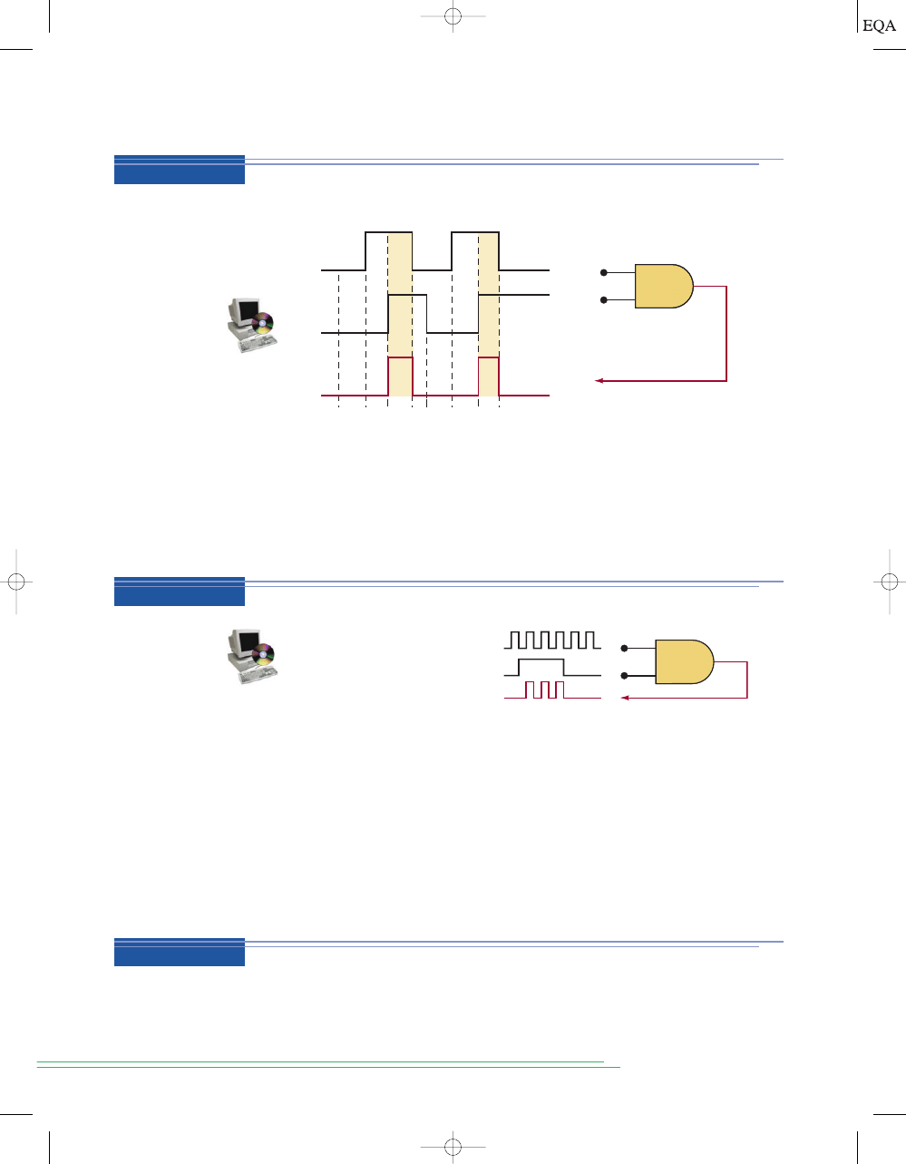
Solution
The OR gate output will be HIGH whenever
any input is HIGH. Between time
t
0
and
t
1
, both inputs are LOW, so OUTPUT
LOW. At t
1
, input
A goes HIGH
while
B remains LOW. This causes OUTPUT to go HIGH at t
1
and stay HIGH
until
t
4
because, during this interval, one or both inputs are HIGH. At
t
4
, input
B goes from 1 to 0 so that now both inputs are LOW, and this drives OUTPUT
back to LOW. At
t
5
,
A goes HIGH, sending OUTPUT back HIGH, where it stays
for the rest of the shown time span.
S
ECTION
3-3/
OR O
PERATION WITH
OR G
ATES
61
Determine the OR gate output in Figure 3-5. The OR gate inputs
A and B are
varying according to the timing diagrams shown. For example,
A starts out
LOW at time
t
0
, goes HIGH at
t
1
, back to LOW at
t
3
, and so on.
Output = A + B
A
t
0
t
1
t
2
t
3
t
4
t
5
t
6
t
7
Time
A
B
1
0
Output
1
0
0
1
B
FIGURE 3-5
Example 3-2.
FIGURE 3-6
Examples
3-3A and B.
For the situation depicted in Figure 3-6, determine the waveform at the OR
gate output.
A + B + C
A
C
B
Time
OUT
A
B
C
0
OUT
1
0
1
0
1
0
1
t
1
Solution
The three OR gate inputs
A, B, and C are varying, as shown by their waveform
diagrams. The OR gate output is determined by realizing that it will be
EXAMPLE 3-2
EXAMPLE 3-3A
TOCCMC03_0131725793.QXD 12/21/05 11:12 AM Page 61

HIGH whenever
any of the three inputs is at a HIGH level. Using this rea-
soning, the OR output waveform is as shown in the figure. Particular atten-
tion should be paid to what occurs at time
t
1
. The diagram shows that, at that
instant of time, input
A is going from HIGH to LOW while input B is going
from LOW to HIGH. Since these inputs are making their transitions at ap-
proximately the same time, and since these transitions take a certain amount
of time, there is a short interval when these OR gate inputs are both in the
undefined range between 0 and 1. When this occurs, the OR gate output also
becomes a value in this range, as evidenced by the glitch or spike on the out-
put waveform at
t
1
. The occurrence of this glitch and its size (amplitude and
width) depend on the speed with which the input transitions occur.
62
C
HAPTER
3/
D
ESCRIBING
L
OGIC
C
IRCUITS
What would happen to the glitch in the output in Figure 3-6 if input
C sat in
the HIGH state while
A and B were changing at time t
1
?
Solution
With the
C input HIGH at t
1
, the OR gate output will remain HIGH, regardless
of what is occurring at the other inputs, because any HIGH input will keep an
OR gate output HIGH. Therefore, the glitch will not appear in the output.
3-4
AND OPERATION WITH AND GATES
The AND operation is the second basic Boolean operation. As an example of
the use of AND logic, consider a typical clothes dryer. It is drying clothes
(heating, tumbling) only if the
timer is set above zero AND the door is closed.
Let’s assign
A to represent timer is set, B to represent door is closed, and x can
represent the
heater and motor are on. The truth table in Figure 3-7(a) shows
what happens when two logic inputs,
A and B, are combined using the AND
operation to produce output
x. The table shows that x is a logic 1 only when
both
A and B are at the logic 1 level. For any case where one of the inputs is
0, the output is 0.
The Boolean expression for the AND operation is
In this expression, the
sign stands for the Boolean AND operation and
not the multiplication operation. However, the AND operation on Boolean
variables operates the same as ordinary multiplication, as examination of
the truth table shows, so we can think of them as being the same. This char-
acteristic can be helpful when evaluating logic expressions that contain
AND operations.
#
x = A
#
B
EXAMPLE 3-3B
REVIEW QUESTIONS
1. What is the only set of input conditions that will produce a LOW output
for any OR gate?
2. Write the Boolean expression for a six-input OR gate.
3. If the
A input in Figure 3-6 is permanently kept at the 1 level, what will
the resultant output waveform be?
TOCCMC03_0131725793.QXD 12/2/05 8:18 PM Page 62
The expression
is read as “
x equals A AND B,” which means
that
x will be 1 only when A and B are both 1. The sign is usually omitted
so that the expression simply becomes
. For the case when three in-
puts are ANDed, we have
This is read as “
x equals A AND
B AND C,” which means that x will be 1 only when A and B and C are all 1.
AND Gate
The logic symbol for a two-input AND gate is shown in Figure 3-7(b). The
AND gate output is equal to the AND product of the logic inputs; that is,
In other words, the AND gate is a circuit that operates so that its out-
put is HIGH only when all its inputs are HIGH. For all other cases, the AND
gate output is LOW.
This same operation is characteristic of AND gates with more than two
inputs. For example, a three-input AND gate and its accompanying truth
table are shown in Figure 3-8. Once again, note that the gate output is 1 only
for the case where
The expression for the output is
For a four-input AND gate, the output is
and so on.
x = ABCD,
x = ABC.
A = B = C = 1.
x = AB.
x = A
#
B
#
C = ABC.
x = AB
#
x = A
#
B
S
ECTION
3-4/
AND O
PERATION WITH
AND G
ATES
63
FIGURE 3-7
(a) Truth
table for the AND opera-
tion; (b) AND gate symbol.
FIGURE 3-8
Truth table
and symbol for a three-
input AND gate.
A
0
0
1
1
B
0
1
0
1
x = A
•
B
0
0
0
1
A
B
(a)
(b)
x = AB
AND
AND gate
A
0
0
0
0
1
1
1
1
B
0
0
1
1
0
0
1
1
C
0
1
0
1
0
1
0
1
x = ABC
0
0
0
0
0
0
0
1
A
C
x = ABC
B
Note the difference between the symbols for the AND gate and the OR
gate. Whenever you see the AND symbol on a logic-circuit diagram, it tells you
that the output will go HIGH
only when all inputs are HIGH. Whenever you
see the OR symbol, it means that the output will go HIGH when
any input is
HIGH.
Summary of the AND Operation
1. The AND operation is performed the same as ordinary multiplication of
1s and 0s.
2. An AND gate is a logic circuit that performs the AND operation on the
circuit’s inputs.
3. An AND gate output will be 1
only for the case when all inputs are 1; for
all other cases, the output will be 0.
4. The expression
is read as “
x equals A AND B.”
x = AB
TOCCMC03_0131725793.QXD 12/2/05 8:18 PM Page 63
Solution
The output of an AND gate is determined by realizing that it will be HIGH only
when all inputs are HIGH at the same time. For the input waveforms given, this
condition is met only during intervals
and
At all other times, one or
more of the inputs are 0, thereby producing a LOW output. Note that input level
changes that occur while the other input is LOW have no effect on the output.
t
6
-
t
7
.
t
2
-
t
3
64
C
HAPTER
3/
D
ESCRIBING
L
OGIC
C
IRCUITS
FIGURE 3-9
Example 3-4.
Determine the output
x from the AND gate in Figure 3-9 for the given input
waveforms.
A
B
x = AB
t
0
t
1
t
2
t
3
0
1
0
1
0
1
A
B
x
t
4
t
5
t
6
t
7
Determine the output waveform for the AND gate shown in Figure 3-10.
What will happen to the
x output waveform in Figure 3-10 if the B input is
kept at the 0 level?
Solution
With
B kept LOW, the x output will also stay LOW. This can be reasoned in
two different ways. First, with
B
0 we have
because
x = A
#
B = A
#
0 = 0
A
B
A
B
x
x
FIGURE 3-10
Examples 3-5A
and B.
Solution
The output
x will be at 1 only when A and B are both HIGH at the same time.
Using this fact, we can determine the
x waveform as shown in the figure.
Notice that the
x waveform is 0 whenever B is 0, regardless of the signal
at
A. Also notice that whenever B is 1, the x waveform is the same as A. Thus,
we can think of the
B input as a control input whose logic level determines
whether or not the
A waveform gets through to the x output. In this situation,
the AND gate is used as an
inhibit circuit. We can say that B
0 is the inhibit
condition producing a 0 output. Conversely,
B
1 is the enable condition,
which enables
A to reach the output. This inhibit operation is an important
application of AND gates, which will be encountered later.
EXAMPLE 3-4
EXAMPLE 3-5A
EXAMPLE 3-5B
TOCCMC03_0131725793.QXD 12/2/05 8:18 PM Page 64
anything multiplied (ANDed) by 0 will be 0. Another way to look at it is that
an AND gate requires that all inputs be HIGH for the output to be HIGH, and
this cannot happen if
B is kept LOW.
S
ECTION
3-5/
NOT O
PERATION
65
3-5
NOT OPERATION
The NOT operation is unlike the OR and AND operations because it can be
performed on a single input variable. For example, if the variable
A is sub-
jected to the NOT operation, the result
x can be expressed as
where the overbar represents the NOT operation. This expression is read as
“
x equals NOT A” or “x equals the inverse of A” or “x equals the complement
of
A.” Each of these is in common usage, and all indicate that the logic value
of
is opposite to the logic value of A. The truth table in Figure 3-11(a)
clarifies this for the two cases
A
0 and A 1. That is,
because 0 is not 1
and
because 1 is not 0
The NOT operation is also referred to as inversion or complementation, and
these terms will be used interchangeably throughout the book. Although we
will always use the overbar indicator to represent inversion, it is important to
mention that another indicator for inversion is the prime symbol ( ). That is,
Both should be recognized as indicating the inversion operation.
A¿ = A
¿
1 = 0
0 = 1
x = A
x = A
FIGURE 3-11
(a) Truth
table; (b) symbol for the
INVERTER (NOT circuit);
(c) sample waveforms.
A
0
1
x = A
1
0
1
0
A
1
0
x
(c)
Presence of small
circle always denotes
inversion
(b)
A
x = A
(a)
NOT
NOT
REVIEW QUESTIONS
1. What is the only input combination that will produce a HIGH at the out-
put of a five-input AND gate?
2. What logic level should be applied to the second input of a two-input
AND gate if the logic signal at the first input is to be inhibited (pre-
vented) from reaching the output?
3.
True or false: An AND gate output will always differ from an OR gate out-
put for the same input conditions.
TOCCMC03_0131725793.QXD 12/2/05 8:18 PM Page 65

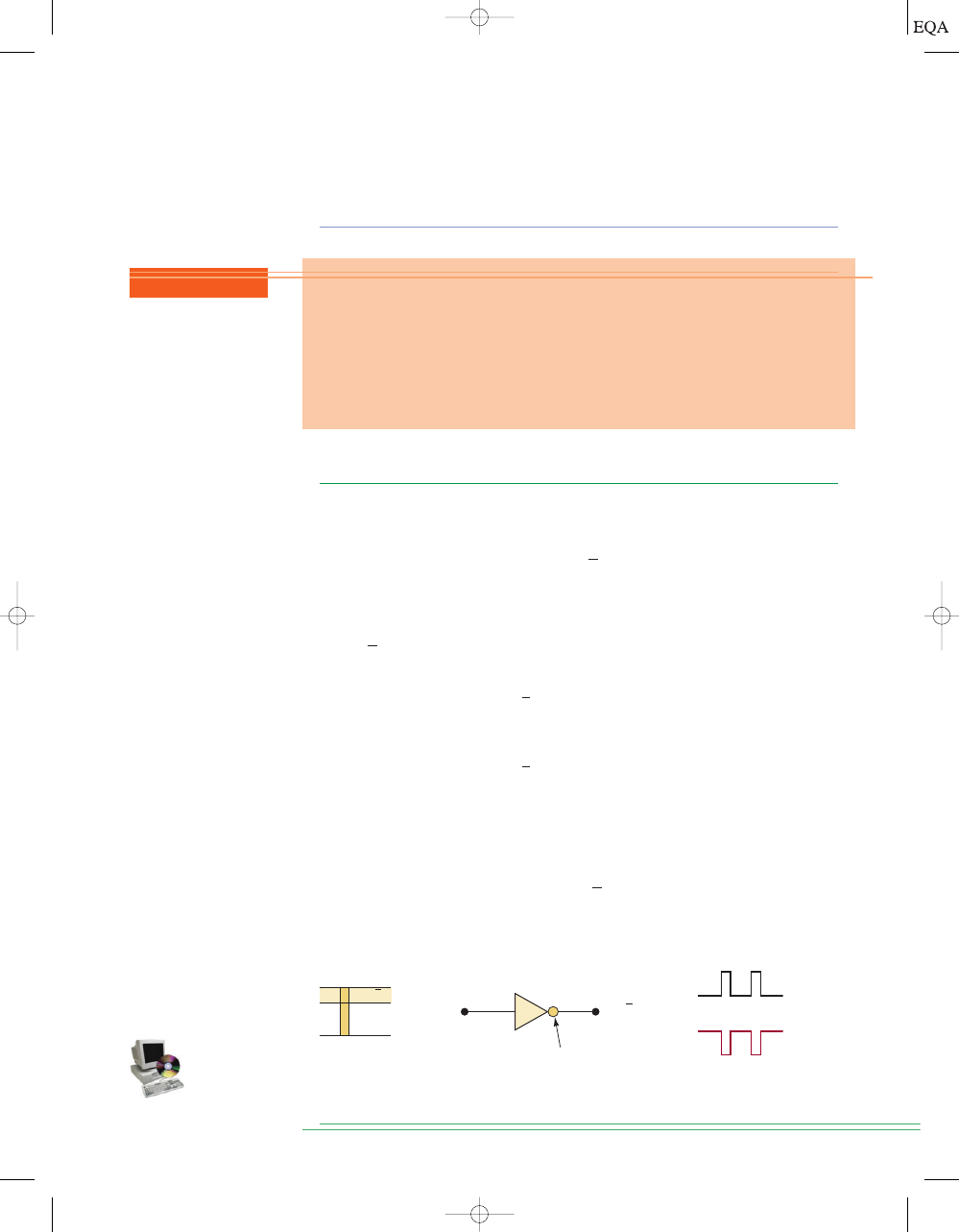
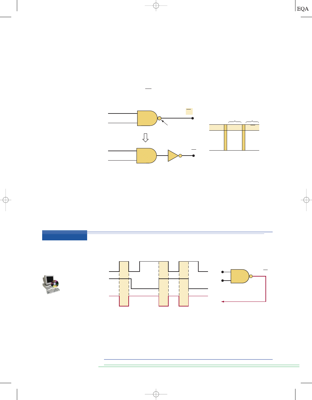
NOT Circuit (INVERTER)
Figure 3-11(b) shows the symbol for a NOT circuit, which is more commonly
called an INVERTER. This circuit
always has only a single input, and its out-
put logic level is always opposite to the logic level of this input. Figure 3-11(c)
shows how the INVERTER affects an input signal. It inverts (complements)
the input signal at all points on the waveform so that whenever the input
0, output 1, and vice versa.
66
C
HAPTER
3/
D
ESCRIBING
L
OGIC
C
IRCUITS
FIGURE 3-12
A NOT gate
indicating a button is
not
pressed when its output is
true.
Logic level 1 (true) when pressed
(false when button is not pressed).
Pressed
+5 V
Push
button
NOT Pressed
Logic level 1 (true) when not pressed
(false when button is pressed).
Summary of Boolean Operations
The rules for the OR, AND, and NOT operations may be summarized as follows:
OR
AND
NOT
1
#
1 = 1
1 + 1 = 1
1
#
0 = 0
1 + 0 = 1
1 = 0
0
#
1 = 0
0 + 1 = 1
0 = 1
0
#
0 = 0
0 + 0 = 0
3-6
DESCRIBING LOGIC CIRCUITS ALGEBRAICALLY
Any logic circuit, no matter how complex, can be described completely using
the three basic Boolean operations because the OR gate, AND gate, and NOT
circuit are the basic building blocks of digital systems. For example, consider
Figure 3-12 shows a typical application of the NOT gate. The push button is
wired to produce a logic 1 (true) when it is pressed. Sometimes we want to
know if the push button is not being pressed, and so this circuit provides an
expression that is true when the button is not pressed.
APPLICATION 3-1
REVIEW QUESTIONS
1. The output of the INVERTER of Figure 3-11 is connected to the input of
a second INVERTER. Determine the output level of the second IN-
VERTER for each level of input
A.
2. The output of the AND gate in Figure 3-7 is connected to the input of an
INVERTER. Write the truth table showing the INVERTER output,
y, for
each combination of inputs
A and B.
TOCCMC03_0131725793.QXD 12/2/05 8:18 PM Page 66
the circuit in Figure 3-13(a). This circuit has three inputs,
A, B, and C, and a
single output,
x. Utilizing the Boolean expression for each gate, we can eas-
ily determine the expression for the output.
The expression for the AND gate output is written
A · B. This AND output
is connected as an input to the OR gate along with
C, another input. The OR
gate operates on its inputs so that its output is the OR sum of the inputs.
Thus, we can express the OR output as
(This final expression
could also be written as
because it does not matter which term
of the OR sum is written first.)
Operator Precedence
Occasionally, there may be confusion about which operation in an expression
is performed first. The expression
can be interpreted in two differ-
ent ways: (1)
is ORed with
C, or (2) A is ANDed with the term
To
avoid this confusion, it will be understood that if an expression contains both
AND and OR operations, the AND operations are performed first, unless
there are
parentheses in the expression, in which case the operation inside
the parentheses is to be performed first. This is the same rule that is used in
ordinary algebra to determine the order of operations.
To illustrate further, consider the circuit in Figure 3-13(b). The expression
for the OR gate output is simply
This output serves as an input to the
AND gate along with another input,
C. Thus, we express the output of the
AND gate as
Note the use of parentheses here to indicate that
A and B are ORed first, before their OR sum is ANDed with C. Without the
parentheses it would be interpreted
incorrectly, because means
that
A is ORed with the product
Circuits Containing INVERTERs
Whenever an INVERTER is present in a logic-circuit diagram, its output ex-
pression is simply equal to the input expression with a bar over it. Figure 3-14
shows two examples using INVERTERs. In Figure 3-14(a), input
A is fed
through an INVERTER, whose output is therefore . The INVERTER output
is fed to an OR gate together with
B, so that the OR output is equal to
Note that the bar is over the
A alone, indicating that A is first inverted and
then ORed with
B.
A + B.
A
B
#
C.
A + B
#
C
x = (A + B)
#
C.
A + B.
B + C.
A
#
B
A
#
B + C
x = C + A
#
B
x = A
#
B + C.
S
ECTION
3-6/
D
ESCRIBING
L
OGIC
C
IRCUITS
A
LGEBRAICALLY
67
FIGURE 3-13
(a) Logic
circuit with its Boolean
expression; (b) logic circuit
whose expression requires
parentheses.
A
B
x = A
•
B + C
C
A
•
B
(a)
A
B
x = ( A + B)
•
C
C
A + B
(b)
A
B
A
B
x = A + B
A + B
(b)
(a)
x = A + B
A
FIGURE 3-14
Circuits
using INVERTERs.
TOCCMC03_0131725793.QXD 12/2/05 8:18 PM Page 67
In Figure 3-14(b), the output of the OR gate is equal to
A
B and is fed
through an INVERTER. The INVERTER output is therefore equal to
because it inverts the
complete input expression. Note that the bar covers the
entire expression (
A
B). This is important because, as will be shown later,
the
expressions and are
not equivalent. The expression
means that
A is ORed with B and then their OR sum is inverted,
whereas the expression
indicates that
A is inverted and B is inverted
and the results are then ORed together.
Figure 3-15 shows two more examples, which should be studied carefully.
Note especially the use of
two separate sets of parentheses in Figure 3-15(b).
Also notice in Figure 3-15(a) that the input variable
A is connected as an in-
put to two different gates.
(
A + B)
(
A + B)
(
A + B)
(
A + B)
(
A + B)
68
C
HAPTER
3/
D
ESCRIBING
L
OGIC
C
IRCUITS
FIGURE 3-15
More examples.
A
B
C
A
D
A
B
C
D
E
A + B
A + D
A
ABC
A + D
(a)
x = ABC ( A + D)
( A + B) C
( A + B) C
(b)
D + ( A + B)C
x = [D + ( A + B) C]
•
E
3-7
EVALUATING LOGIC-CIRCUIT OUTPUTS
Once we have the Boolean expression for a circuit output, we can obtain the
output logic level for any set of input levels. For example, suppose that we
want to know the logic level of the output
x for the circuit in Figure 3-15(a)
for the case where
and
As in ordinary algebra,
D = 1.
A = 0,
B = 1,
C = 1,
REVIEW QUESTIONS
1. In Figure 3-15(a), change each AND gate to an OR gate, and change the
OR gate to an AND gate. Then write the expression for output
x.
2. In Figure 3-15(b), change each AND gate to an OR gate, and each OR
gate to an AND gate. Then write the expression for
x.
TOCCMC03_0131725793.QXD 12/2/05 8:18 PM Page 68

the value of
x can be found by “plugging” the values of the variables into the
expression and performing the indicated operations as follows:
As another illustration, let us evaluate the output of the circuit in Figure
3-15(b) for
and
In general, the following rules must always be followed when evaluating a
Boolean expression:
1. First, perform all inversions of single terms; that is,
or
2. Then perform all operations within parentheses.
3. Perform an AND operation before an OR operation unless parentheses
indicate otherwise.
4. If an expression has a bar over it, perform the operations inside the ex-
pression first and then invert the result.
For practice, determine the outputs of both circuits in Figure 3-15 for the
case where all inputs are 1. The answers are
and
respectively.
Analysis Using a Table
Whenever you have a combinational logic circuit and you want to know how
it works, the best way to analyze it is to use a truth table. The advantages of
this method are:
It allows you to analyze one gate or logic combination at a time.
It allows you to easily double-check your work.
When you are done, you have a table that is of tremendous benefit in
troubleshooting the logic circuit.
Recall that a truth table lists all the possible input combinations in nu-
merical order. For each possible input combination, we can determine the logic
state at every point (node) in the logic circuit including the output. For exam-
ple refer to Figure 3-16(a). There are several intermediate nodes in this circuit
that are neither inputs nor outputs to the circuit. They are simply connections
between one gate’s output and another gate’s input. In this diagram they have
been labeled
u, v, and w. The first step after listing all the input combinations
is to create a column in the truth table for each intermediate signal (node) as
shown in Figure 3-16(b). Node
u has been filled in as the complement of A.
x = 1,
x = 0
1 = 0.
0 = 1
=
1
=
1
#
1
=
[1 + 1]
#
1
=
[1 + 0]
#
1
=
[1 + 0
#
1]
#
1
=
[1 + (0 + 0)
#
1]
#
1
x
=
[
D + (A + B)C]
#
E
E = 1.
A = 0,
B = 0,
C = 1,
D = 1,
= 0
= 1
#
1
#
1
#
0
= 1
#
1
#
1
#
(1)
= 1
#
1
#
1
#
(0 + 1)
= 0
#
1
#
1
#
(0 + 1)
x = ABC(A + D)
S
ECTION
3-7/
E
VALUATING
L
OGIC
-C
IRCUIT
O
UTPUTS
69
TOCCMC03_0131725793.QXD 12/2/05 8:18 PM Page 69
The next step is to fill in the values for column
v as shown in Figure 3-16(c).
From the diagram we can see that
The node
v should be HIGH when
(node
u) is HIGH AND B is HIGH. This occurs whenever A is LOW AND B
is HIGH. The third step is to predict the values at node
w which is the logical
product of
BC. This column is HIGH whenever B is HIGH AND C is HIGH as
shown in Figure 3-16(d). The final step is to logically combine columns
v and
w to predict the output x. Since the
x output will be HIGH when
v is HIGH OR w is HIGH as shown in Figure 3-16(e).
If you built this circuit and it was not producing the correct output for
x
under all conditions, this table could be used to find the trouble. The general
procedure is to test the circuit under each combination of inputs. If any in-
put combination produces an incorrect output (i.e., a fault), compare the
actual logic state of each intermediate node in the circuit with the correct
theoretical value in the table while applying that input condition. If the logic
state for an intermediate node is
correct, the problem must be farther to the
right of that node. If the logic state for an intermediate node is
incorrect, the
problem must be to the left of that node (or that node is shorted to some-
thing). Detailed troubleshooting procedures and possible circuit faults will
be covered more extensively in Chapter 4.
x = v + w,
A
v = AB.
70
C
HAPTER
3/
D
ESCRIBING
L
OGIC
C
IRCUITS
FIGURE 3-16
Analysis of
a logic circuit using truth
tables.
u = A
v = AB
x
A
B
C
w = BC
A
B
C u=
A
v=
AB
w=
BC
x=
v+w
0
0
1
0
0
1
0
1
1
0
1
1
1
0
0
1
0
0
1
1
0
1
1
0
1
0
1
0
1
0
1
0
(b)
A
B
C u=
A
v=
AB
w=
BC
x=
v+w
(c)
0
0
0
1
0
0
0
1
1
0
0
1
0
1
1
0
1
1
1
1
1
0
0
0
0
1
0
1
0
0
1
1
0
0
0
1
1
1
0
0
A
B
C u=
A
v=
AB
w=
BC
x=
v+w
0
0
0
1
0
0
0
0
1
1
0
0
0
1
0
1
1
0
0
1
1
1
1
1
1
0
0
0
0
0
1
0
1
0
0
0
1
1
0
0
0
0
1
1
1
0
0
1
(d)
0
0
0
0
0
0
1
0
0
0
0
0
1
0
1
0
1
1
1
1
1
0
0
0
0
1
1
0
0
0
1
0
0
0
0
1
0
0
1
1
0
0
1
1
1
1
1
1
1
0
0
0
0
0
1
1
A
B
C u=
A
v=
AB
w=
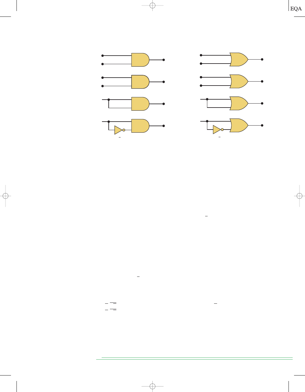
BC
x=
v+w
(e)
(a)
TOCCMC03_0131725793.QXD 12/21/05 11:12 AM Page 70
3-8
IMPLEMENTING CIRCUITS FROM BOOLEAN EXPRESSIONS
When the operation of a circuit is defined by a Boolean expression, we can
draw a logic-circuit diagram directly from that expression. For example, if we
needed a circuit that was defined by
, we would immediately
know that all that was needed was a three-input AND gate. If we needed a
circuit that was defined by
, we would use a two-input OR gate
with an INVERTER on one of the inputs. The same reasoning used for these
simple cases can be extended to more complex circuits.
x = A + B
x = A
#
B
#
C
S
ECTION
3-8/
I
MPLEMENTING
C
IRCUITS FROM
B
OOLEAN
E
XPRESSIONS
71
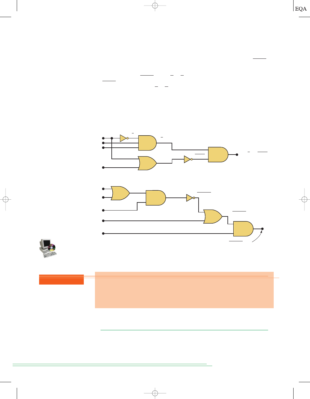
Analyze the operation of Figure 3-15(a) by creating a table showing the logic
state at each node of the circuit.
Solution
Fill in the column for
t by entering a 1 for all entries where A
0 and
B
1 and C 1.
Fill in the column for
u by entering a 1 for all entries where A
1 or D 1.
Fill in the column for
v by complementing all entries in column u.
Fill in the column for
x by entering a 1 for all entries where t
l and v 1.
A
B
C
D
t
u
A D
v
x
tv
0
0
0
0
0
0
1
0
0
0
0
1
0
1
0
0
0
0
1
0
0
0
1
0
0
0
1
1
0
1
0
0
0
1
0
0
0
0
1
0
0
1
0
1
0
1
0
0
0
1
1
0
1
0
1
1
0
1
1
1
1
1
0
0
1
0
0
0
0
1
0
0
1
0
0
1
0
1
0
0
1
0
1
0
0
1
0
0
1
0
1
1
0
1
0
0
1
1
0
0
0
1
0
0
1
1
0
1
0
1
0
0
1
1
1
0
0
1
0
0
1
1
1
1
0
1
0
0
A
D
ABC
EXAMPLE 3-6
REVIEW QUESTIONS
1. Use the expression for
x to determine the output of the circuit in Figure
3-15(a) for the conditions
and
2. Use the expression for
x to determine the output of the circuit in Figure
3-15(b) for the conditions
3. Determine the answers to Questions 1 and 2 by finding the logic levels
present at each gate output using a table as in Figure 3-16.
A = B = E = 1,
C = D = 0.
D = 0.
A = 0,
B = 1,
C = 1,
TOCCMC03_0131725793.QXD 12/2/05 8:18 PM Page 71

Suppose that we wanted to construct a circuit whose output is
This Boolean expression contains three terms
which are ORed together. This tells us that a three-input OR
gate is required with inputs that are equal to
AC,
, and
This is illus-
trated in Figure 3-17(a), where a three-input OR gate is drawn with inputs la-
beled as
AC,
, and
ABC.
BC
ABC.
BC
(
AC,
BC,
ABC),
y = AC + BC + ABC.
72
C
HAPTER
3/
D
ESCRIBING
L
OGIC
C
IRCUITS
FIGURE 3-17
Constructing
a logic circuit from a
Boolean expression.
AC
ABC
BC
y = AC + BC + ABC
(a)
y = AC + BC + ABC
A
B
C
C
A
B
AC
ABC
BC
(b)
C
C
B
Each OR gate input is an AND product term, which means that an AND
gate with appropriate inputs can be used to generate each of these terms.
This is shown in Figure 3-17(b), which is the final circuit diagram. Note the
use of INVERTERs to produce the
and terms required in the expression.
This same general approach can always be followed, although we shall
find that there are some clever, more efficient techniques that can be em-
ployed. For now, however, this straightforward method will be used to mini-
mize the number of new items that are to be learned.
C
A
Draw the circuit diagram to implement the expression
Solution
This expression shows that the terms
A
B and
are inputs to an AND
gate, and each of these two terms is generated from a separate OR gate. The
result is drawn in Figure 3-18.
B + C
x = (A + B)(B + C).
A
B
C
A + B
B + C
B
x = (A + B)(B + C)
FIGURE 3-18
Example 3-7.
EXAMPLE 3-7
TOCCMC03_0131725793.QXD 12/2/05 8:18 PM Page 72
3-9
NOR GATES AND NAND GATES
Two other types of logic gates, NOR gates and NAND gates, are widely used
in digital circuits. These gates actually combine the basic AND, OR, and
NOT operations, so it is a relatively simple matter to write their Boolean
expressions.
NOR Gate
The symbol for a two-input NOR gate is shown in Figure 3-19(a). It is the
same as the OR gate symbol except that it has a small circle on the output.
The small circle represents the inversion operation. Thus, the NOR gate op-
erates like an OR gate followed by an INVERTER, so that the circuits in
Figure 3-19(a) and (b) are equivalent, and the output expression for the NOR
gate is
x = A + B.
S
ECTION
3-9/
NOR G
ATES AND
NAND G
ATES
73
FIGURE 3-19
(a) NOR
symbol; (b) equivalent circuit;
(c) truth table.
A
0
0
1
1
B
0
1
0
1
A + B
0
1
1
1
A + B
1
0
0
0
A
B
Denotes
inversion
(a)
(b)
OR
NOR
(c)
x = A + B
A + B
A
B
x = A + B
The truth table in Figure 3-19(c) shows that the NOR gate output is the
exact inverse of the OR gate output for all possible input conditions. An OR
gate output goes HIGH when any input is HIGH; the NOR gate output goes
LOW when any input is HIGH. This same operation can be extended to NOR
gates with more than two inputs.
REVIEW QUESTIONS
1. Draw the circuit diagram that implements the expression
using gates with no more than three inputs.
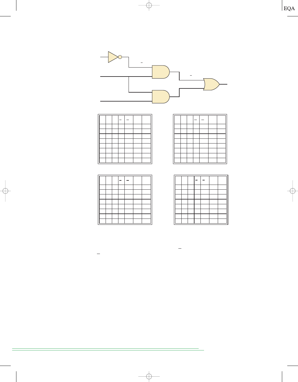
2. Draw the circuit diagram for the expression
3. Draw the circuit diagram for
x = [D + (A + B)C)]
#
E.
y = AC + BC + ABC.
x = ABC(A + D)
TOCCMC03_0131725793.QXD 12/2/05 8:18 PM Page 73
Solution
One way to determine the NOR output waveform is to find first the OR out-
put waveform and then invert it (change all 1s to 0s, and vice versa). Another
way utilizes the fact that a NOR gate output will be HIGH
only when all in-
puts are LOW. Thus, you can examine the input waveforms, find those time
intervals where they are all LOW, and make the NOR output HIGH for those
intervals. The NOR output will be LOW for all other time intervals. The re-
sultant output waveform is shown in the figure.
74
C
HAPTER
3/
D
ESCRIBING
L
OGIC
C
IRCUITS
FIGURE 3-20
Example 3-8.
Determine the waveform at the output of a NOR gate for the input wave-
forms shown in Figure 3-20.
Determine the Boolean expression for a three-input NOR gate followed by
an INVERTER.
Solution
Refer to Figure 3-21, where the circuit diagram is shown. The expression at
the NOR output is
which is then fed through an INVERTER to
produce
The presence of the double inversion signs indicates that the quantity (
A
B
C) has been inverted and then inverted again. It should be clear that this
simply results in the expression (
A
B C) being unchanged. That is,
Whenever two inversion bars are over the same variable or quantity, they
cancel each other out, as in the example above. However, in cases such as
the inversion bars do not cancel. This is because the smaller inver-
sion bars invert the single variables
A and B, while the wide bar inverts the
quantity (
). Thus,
. Similarly,
.
A B Z AB
A + B Z A + B
A + B
A + B
x = (A + B + C) = (A + B + C)
x = (A + B + C)
(
A + B + C),
A
B
x = A + B
1
0
A
1
0
B
1
0
x
A
C
B
A + B + C
x = A + B + C = A + B + C
FIGURE 3-21
Example 3-9.
EXAMPLE 3-8
EXAMPLE 3-9
TOCCMC03_0131725793.QXD 12/2/05 8:18 PM Page 74
NAND Gate
The symbol for a two-input NAND gate is shown in Figure 3-22(a). It is the
same as the AND gate symbol except for the small circle on its output. Once
again, this small circle denotes the inversion operation. Thus, the NAND op-
erates like an AND gate followed by an INVERTER, so that the circuits of
Figure 3-22(a) and (b) are equivalent, and the output expression for the
NAND gate is
x = AB.
S
ECTION
3-9/
NOR G
ATES AND
NAND G
ATES
75
FIGURE 3-22
(a) NAND
symbol; (b) equivalent
circuit; (c) truth table.
A
0
0
1
1
B
0
1
0
1
AB
0
0
0
1
(c)
AB
1
1
1
0
AND
NAND
A
B
Denotes
inversion
(a)
(b)
x = AB
A
B
AB
AB
The truth table in Figure 3-22(c) shows that the NAND gate output is the
exact inverse of the AND gate for all possible input conditions. The AND
output goes HIGH only when all inputs are HIGH, while the NAND output
goes LOW only when all inputs are HIGH. This same characteristic is true of
NAND gates having more than two inputs.
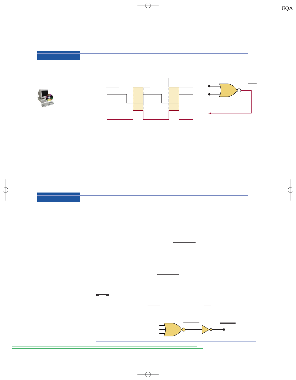
Determine the output waveform of a NAND gate having the inputs shown in
Figure 3-23.
A
B
x
x = AB
A
B
FIGURE 3-23
Example 3-10.
Solution
One way is to draw first the output waveform for an AND gate and then in-
vert it. Another way utilizes the fact that a NAND output will be LOW only
when all inputs are HIGH. Thus, you can find those time intervals during
which the inputs are all HIGH, and make the NAND output LOW for those in-
tervals. The output will be HIGH at all other times.
EXAMPLE 3-10
TOCCMC03_0131725793.QXD 12/2/05 8:18 PM Page 75
76
C
HAPTER
3/
D
ESCRIBING
L
OGIC
C
IRCUITS
FIGURE 3-24
Examples 3-11 and 3-12.
Implement the logic circuit that has the expression
using
only NOR and NAND gates.
Solution
The
term is the expression for the output of a NOR gate. This term is
ANDed with
A and B, and the result is inverted; this, of course, is the NAND
operation. Thus, the circuit is implemented as shown in Figure 3-24. Note
that the NAND gate first ANDs the
A, B, and
terms, and then it in-
verts the
complete result.
(
C + D)
(
C + D)
x = AB
#
(
C + D)
C
D
1
0
C + D
x = AB(C + D)
1
1
1
0
B
A
Determine the output level in Figure 3-24 for
A
B C 1 and D 0.
Solution
In the first method we use the expression for
x.
In the second method, we write down the input logic levels on the circuit
diagram (shown in color in Figure 3-24) and follow these levels through
each gate to the final output. The NOR gate has inputs of 1 and 0 to pro-
duce an output of 0 (an OR would have produced an output of 1). The
NAND gate thus has input levels of 0, 1, and 1 to produce an output of 1 (an
AND would have produced an output of 0).
= 0 = 1
= 1
#
1
#
0
= 1
#
1
#
(1)
= 1
#
1
#
(1 + 0)
x = AB(C + D)
3-10
BOOLEAN THEOREMS
We have seen how Boolean algebra can be used to help analyze a logic circuit
and express its operation mathematically. We will continue our study of
Boolean algebra by investigating the various Boolean theorems (rules) that
can help us to simplify logic expressions and logic circuits. The first group of
theorems is given in Figure 3-25. In each theorem,
x is a logic variable that
EXAMPLE 3-11
EXAMPLE 3-12
REVIEW QUESTIONS
1. What is the only set of input conditions that will produce a HIGH output
from a three-input NOR gate?
2. Determine the output level in Figure 3-24 for
A
B 1, C D 0.
3. Change the NOR gate of Figure 3-24 to a NAND gate, and change the
NAND to a NOR. What is the new expression for
x?
TOCCMC03_0131725793.QXD 12/2/05 8:18 PM Page 76
can be either a 0 or a 1. Each theorem is accompanied by a logic-circuit dia-
gram that demonstrates its validity.
Theorem (1) states that if any variable is ANDed with 0, the result must
be 0. This is easy to remember because the AND operation is just like ordi-
nary multiplication, where we know that anything multiplied by 0 is 0. We
also know that the output of an AND gate will be 0 whenever any input is 0,
regardless of the level on the other input.
Theorem (2) is also obvious by comparison with ordinary multiplication.
Theorem (3) can be proved by trying each case. If
x
0, then ;
if
x
1, then Thus,
Theorem (4) can be proved in the same manner. However, it can also be
reasoned that at any time either
x or its inverse
must be at the 0 level, and
so their AND product always must be 0.
Theorem (5) is straightforward, since 0
added to anything does not affect
its value, either in regular addition or in OR addition.
Theorem (6) states that if any variable is ORed with 1, the result will al-
ways be 1. We check this for both values of
x: 0
1 1 and 1 1 1.
Equivalently, we can remember that an OR gate output will be 1 when
any
input is 1, regardless of the value of the other input.
Theorem (7) can be proved by checking for both values of
x: 0
0 0
and 1
1 1.
Theorem (8) can be proved similarly, or we can just reason that at any
time either
x or must be at the 1 level so that we are always ORing a 0 and
a 1, which always results in 1.
Before introducing any more theorems, we should point out that when the-
orems (1) through (8) are applied, the variable
x may actually represent an
expression containing more than one variable. For example, if we have
we can invoke theorem (4) by letting
Thus, we can say that
The same idea can be applied to the use of any of these theorems.
Multivariable Theorems
The theorems presented below involve more than one variable:
(9)
x
y y x
(10)
x
#
y = y
#
x
AB(AB) = 0.
x = AB.
AB(AB),
x
x
x
#
x = x.
1
#
1 = 1.
0
#
0 = 0
S
ECTION
3-10/
B
OOLEAN
T
HEOREMS
77
FIGURE 3-25
Single-variable theorems.
0
x
x
0
x
1
x
1
x
x
1
x
0
x
x
x
1
x
x
0
(1) x
•
0 = 0
(2) x
•
1 = x
(3) x
•
x = x
(4) x
•
x = 0
(5) x + 0 = x
(6) x + 1 = 1
(7) x + x = x
(8) x + x = 1
TOCCMC03_0131725793.QXD 12/2/05 8:18 PM Page 77

x
y
xy
x
xy
0
0
0
0
0
1
0
0
1
0
0
1
1
1
1
1
(11)
x
(y z) (x y) z x y z
(12)
x(yz)
(xy)z xyz
(13
a)
x(y
z) xy xz
(13
b)
(
w
x)(y z) wy xy wz xz
(14)
x
xy x
(15
a)
(15
b)
Theorems (9) and (10) are called the
commutative laws. These laws indi-
cate that the order in which we OR or AND two variables is unimportant; the
result is the same.
Theorems (11) and (12) are the
associative laws, which state that we can
group the variables in an AND expression or OR expression any way we want.
Theorem (13) is the
distributive law, which states that an expression can be
expanded by multiplying term by term just the same as in ordinary algebra.
This theorem also indicates that we can factor an expression. That is, if we have
a sum of two (or more) terms, each of which contains a common variable, the
common variable can be factored out just as in ordinary algebra. For example,
if we have the expression
we can factor out the
variable:
As another example, consider the expression
ABC
ABD. Here the two
terms have the variables
A and B in common, and so
can be factored out
of both terms. That is,
ABC
ABD AB(C D)
Theorems (9) to (13) are easy to remember and use because they are
identical to those of ordinary algebra. Theorems (14) and (15), on the other
hand, do not have any counterparts in ordinary algebra. Each can be proved
by trying all possible cases for
x and y. This is illustrated (for theorem 14) by
creating an analysis table for the equation
x
xy as follows:
A
#
B
ABC + A
B
C = B(AC + A
C)
B
ABC + A
B
C,
x + xy = x + y
x + xy = x + y
78
C
HAPTER
3/
D
ESCRIBING
L
OGIC
C
IRCUITS
Notice that the value of the entire expression (
x
xy) is always the same
as
x.
Theorem (14) can also be proved by factoring and using theorems (6) and
(2) as follows:
All of these Boolean theorems can be useful in simplifying a logic expres-
sion—that is, in reducing the number of terms in the expression. When this is
done, the reduced expression will produce a circuit that is less complex than
the one that the original expression would have produced. A good portion of
the next chapter will be devoted to the process of circuit simplification. For
=
x
[using theorem (2)]
=
x
#
1
[using theorem (6)]
x + xy = x(1 + y)
TOCCMC03_0131725793.QXD 12/2/05 8:18 PM Page 78

now, the following examples will serve to illustrate how the Boolean theo-
rems can be applied. Note: You can find all the Boolean theorems on the in-
side back cover.
S
ECTION
3-10/
B
OOLEAN
T
HEOREMS
79
Simplify the expression
.
Solution
Factor out the common variables
using theorem (13):
Using theorem (8), the term in parentheses is equivalent to 1. Thus,
[using theorem (2)]
=
AB
y = AB
#
1
y = AB(D + D)
AB
y = ABD + AB
D
Simplify
Solution
The expression can be expanded by multiplying out the terms [theorem (13)]:
Invoking theorem (4), the term
Also,
[theorem (3)]:
Factoring out the variable
B [theorem (13)], we have
Finally, using theorems (2) and (6),
z
B
z = B(A + A + 1)
z = 0 + A
#
B + B
#
A + B = AB + AB + B
B
#
B = B
A
#
A = 0.
z = A
#
A + A
#
B + B
#
A + B
#
B
z = (A + B)(A + B).
Simplify
Solution
Factoring out the common variables
CD, we have
Utilizing theorem (15a), we can replace
by
A
B, so
=
ACD + BCD
x = CD(A + B)
A + AB
x = CD(A + AB)
x =
ACD + ABCD.
EXAMPLE 3-13
EXAMPLE 3-14
EXAMPLE 3-15
TOCCMC03_0131725793.QXD 12/2/05 8:18 PM Page 79

3-11
DEMORGAN’S THEOREMS
Two of the most important theorems of Boolean algebra were contributed by
a great mathematician named DeMorgan. DeMorgan’s theorems are ex-
tremely useful in simplifying expressions in which a product or sum of vari-
ables is inverted. The two theorems are:
(16)
(17)
Theorem (16) says that when the OR sum of two variables is inverted,
this is the same as inverting each variable individually and then ANDing
these inverted variables. Theorem (17) says that when the AND product of
two variables is inverted, this is the same as inverting each variable individ-
ually and then ORing them. Each of DeMorgan’s theorems can readily be
proven by checking for all possible combinations of
x and y. This will be left
as an end-of-chapter exercise.
Although these theorems have been stated in terms of single variables
x
and
y, they are equally valid for situations where x and/or y are expressions
that contain more than one variable. For example, let’s apply them to the ex-
pression
as shown below:
Note that we used theorem (16) and treated
as
x and C as y. The result can
be further simplified because we have a product
that is inverted. Using
theorem (17), the expression becomes
Notice that we can replace
by
B, so that we finally have
This final result contains only inverter signs that invert a single variable.
(
A + B)
#
C = A
C + BC
B
AB
#
C = (A + B)
#
C
AB
AB
(
AB + C) = (AB)
#
C
(
AB + C)
(
x
#
y) = x + y
(
x + y) = x
#
y
80
C
HAPTER
3/
D
ESCRIBING
L
OGIC
C
IRCUITS
Simplify the expression
to one having only single vari-
ables inverted.
Solution
Using theorem (17), and treating (
) as
x and (
) as
y, we have
z = (A + C) + (B + D)
B + D
A + C
z = (A + C)
#
(
B + D)
REVIEW QUESTIONS
1. Use theorems (13) and (14) to simplify
2. Use theorems (13) and (8) to simplify
3. Use theorems (13) and (15b) to simplify
y = AD + ABD.
y = A
BCD + A
B
C
D.
y = AC + ABC.
EXAMPLE 3-16
TOCCMC03_0131725793.QXD 12/2/05 8:18 PM Page 80

We can think of this as breaking the large inverter sign down the middle
and changing the AND sign ( ) to an OR sign (
). Now the term
can
be simplified by applying theorem (16). Likewise,
can be simpli-
fied:
Here we have broken the larger inverter signs down the middle and replaced
the (
) with a (·). Canceling out the double inversions, we have finally
Example 3-16 points out that when using DeMorgan’s theorems to reduce
an expression, we may break an inverter sign at any point in the expression
and change the operator sign at that point in the expression to its opposite
(
is changed to ·, and vice versa). This procedure is continued until the ex-
pression is reduced to one in which only single variables are inverted. Two
more examples are given below.
Example 1
Example 2
DeMorgan’s theorems are easily extended to more than two variables.
For example, it can be proved that
Here, we see that the large inverter sign is broken at
two points in the expres-
sion and the operator sign is changed to its opposite. This can be extended to
any number of variables. Again, realize that the variables can themselves be
expressions rather than single variables. Here is another example.
AB CD EF
Implications of DeMorgan’s Theorems
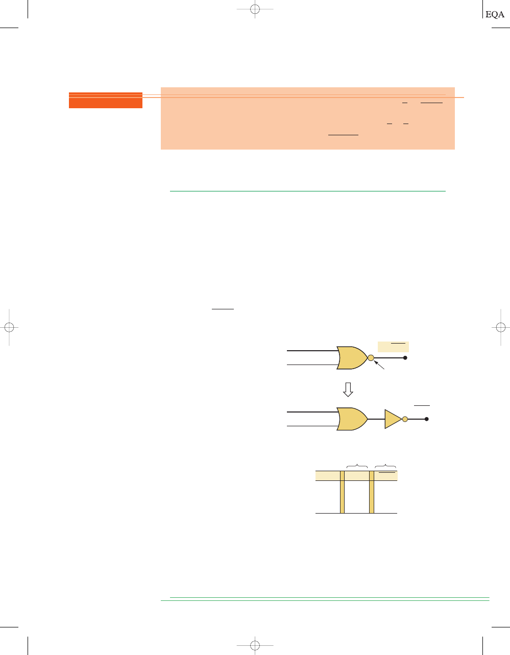
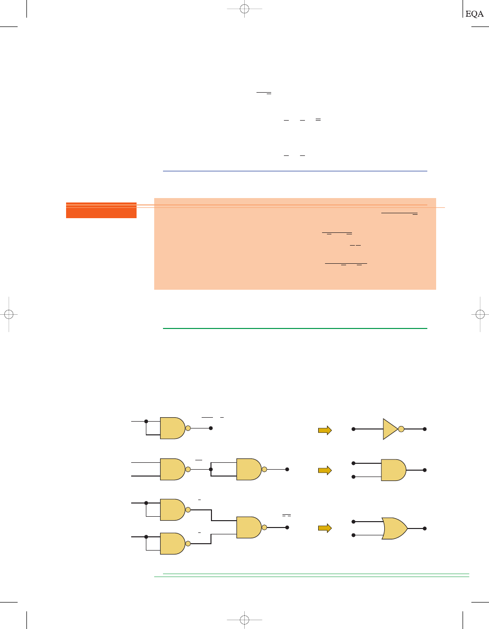
Let us examine theorems (16) and (17) from the standpoint of logic circuits.
First, consider theorem (16):
The left-hand side of the equation can be viewed as the output of a NOR gate
whose inputs are
x and y. The right-hand side of the equation, on the other
x + y = x
#
y
=
AB + CD + EF
x = AB
#
CD
#
EF
x
#
y
#
z = x + y + z
x + y + z = x
#
y
#
z
=
A
B + A
C + D
E + D
F
=
[
A
#
(
B + C)] + [D
#
(
E + F)]
=
A
#
(
B + C)
=
(
A
#
BC) + (D
#
EF)
=
A
#
(
B + C)
=
(
A + BC) + (D + EF)
=
A
#
(
B
#
C)
1A + BC2
1D + EF2
z = A + B
#
C
z = AC + B D
= (
A
#
C) + B
#
D
z = (A + C) + (B + D)
(
B + D)
(
A + C)
#
S
ECTION
3-11/
D
E
M
ORGAN
’
S
T
HEOREMS
81
TOCCMC03_0131725793.QXD 12/2/05 8:18 PM Page 81
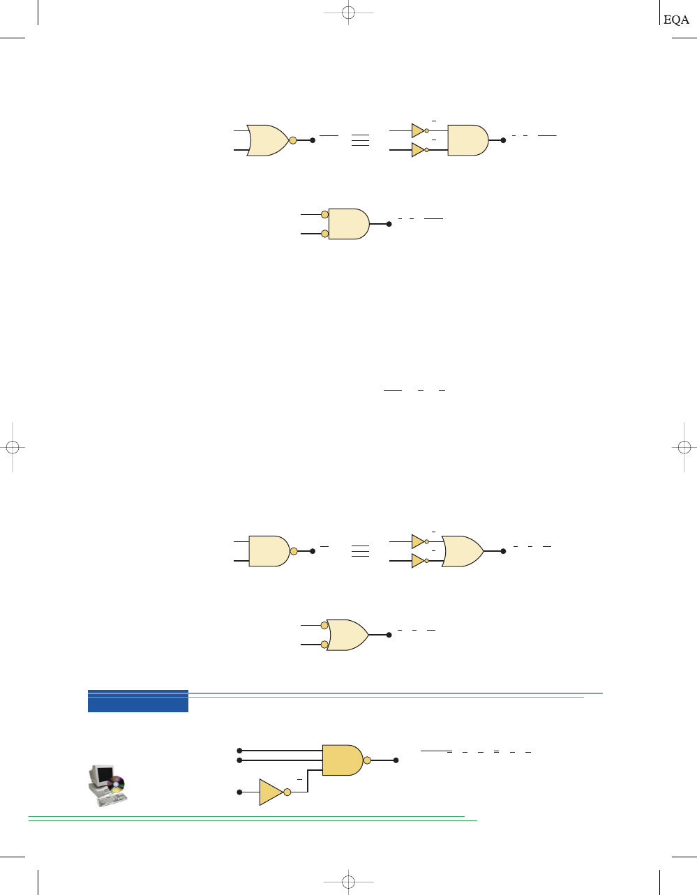
hand, is the result of first inverting both
x and y and then putting them through
an AND gate. These two representations are equivalent and are illustrated in
Figure 3-26(a). What this means is that an AND gate with INVERTERs on each
of its inputs is equivalent to a NOR gate. In fact, both representations are used
to represent the NOR function. When the AND gate with inverted inputs is used
to represent the NOR function, it is usually drawn as shown in Figure 3-26(b),
where the small circles on the inputs represent the inversion operation.
Now consider theorem (17):
The left side of the equation can be implemented by a NAND gate with in-
puts
x and y. The right side can be implemented by first inverting inputs x
and
y and then putting them through an OR gate. These two equivalent rep-
resentations are shown in Figure 3-27(a). The OR gate with INVERTERs on
each of its inputs is equivalent to the NAND gate. In fact, both representa-
tions are used to represent the NAND function. When the OR gate with in-
verted inputs is used to represent the NAND function, it is usually drawn as
shown in Figure 3-27(b), where the circles again represent inversion.
x
#
y = x + y
82
C
HAPTER
3/
D
ESCRIBING
L
OGIC
C
IRCUITS
FIGURE 3-26
(a) Equivalent circuits
implied by theorem (16);
(b) alternative symbol for
the NOR function.
FIGURE 3-27
(a) Equivalent circuits
implied by theorem (17);
(b) alternative symbol for
the NAND function.
(b)
x
y
x
•
y = x + y
x
y
(a)
x
y
x
y
x + y
x
•
y = x + y
Determine the output expression for the circuit of Figure 3-28 and simplify
it using DeMorgan’s theorems.
A
B
C
z = A
•
B
•
C = A + B + C = A + B + C
C
(b)
x
y
x + y = xy
x
y
x + y = xy
xy
(a)
x
y
x
y
FIGURE 3-28
Example 3-17.
EXAMPLE 3-17
TOCCMC03_0131725793.QXD 12/2/05 8:18 PM Page 82
Solution
The expression for
z is
Use DeMorgan’s theorem to break the large
inversion sign:
Cancel the double inversions over
C to obtain
z = A + B + C
z = A + B + C
z = ABC.
S
ECTION
3-12/
U
NIVERSALITY OF
NAND G
ATES AND
NOR G
ATES
83
3-12
UNIVERSALITY OF NAND GATES AND NOR GATES
All Boolean expressions consist of various combinations of the basic opera-
tions of OR, AND, and INVERT. Therefore, any expression can be imple-
mented using combinations of OR gates, AND gates, and INVERTERs. It is
possible, however, to implement any logic expression using
only NAND gates
and no other type of gate. This is because NAND gates, in the proper combi-
nation, can be used to perform each of the Boolean operations OR, AND, and
INVERT. This is demonstrated in Figure 3-29.
A
A
B
A
B
A
INVERTER
AND
OR
A
A
B
B
1
2
3
1
2
(a)
(b)
(c)
x = A
•
A = A
AB
A
B
x = AB
x = A B = A + B
FIGURE 3-29
NAND gates can be used to implement any Boolean function.
REVIEW QUESTIONS
1. Use DeMorgan’s theorems to convert the expression
to
one that has only single-variable inversions.
2. Repeat question 1 for the expression
3. Implement a circuit having output expression
using only a NOR
gate and an INVERTER.
4. Use DeMorgan’s theorems to convert
y
to an expression
containing only single-variable inversions.
A + B + CD
z = A
BC
y = RST + Q.
z = (A + B)
#
C
TOCCMC03_0131725793.QXD 12/2/05 8:18 PM Page 83
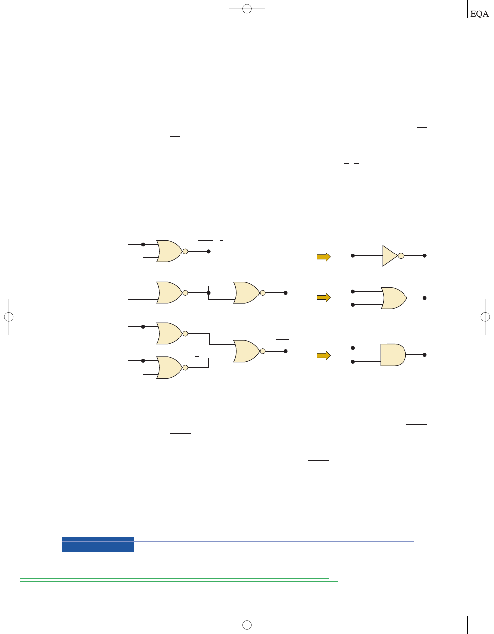
First, in Figure 3-29(a), we have a two-input NAND gate whose inputs are
purposely connected together so that the variable
A is applied to both. In
this configuration, the NAND simply acts as INVERTER because its output
is
In Figure 3-29(b), we have two NAND gates connected so that the AND
operation is performed. NAND gate 2 is used as an INVERTER to change
to
which is the desired AND function.
The OR operation can be implemented using NAND gates connected as
shown in Figure 3-29(c). Here NAND gates 1 and 2 are used as INVERTERs
to invert the inputs, so that the final output is
which can be sim-
plified to
x
A B using DeMorgan’s theorem.
In a similar manner, it can be shown that NOR gates can be arranged to
implement any of the Boolean operations. This is illustrated in Figure 3-30.
Part (a) shows that a NOR gate with its inputs connected together behaves
as an INVERTER because the output is
x = A + A = A.
x = A
#
B,
AB = AB,
AB
x = A
#
A = A.
84
C
HAPTER
3/
D
ESCRIBING
L
OGIC
C
IRCUITS
FIGURE 3-30
NOR gates can be used to implement any Boolean operation.
A
INVERTER
A
B
OR
A
B
AND
A
A
A
B
B
(a)
(b)
(c)
A
B
x = A + B = A B
x = A + A = A
A + B
A + B
2
3
1
1
2
In Figure 3-30(b), two NOR gates are arranged so that the OR opera-
tion is performed. NOR gate 2 is used as an INVERTER to change
to
which is the desired OR function.
The AND operation can be implemented with NOR gates as shown in
Figure 3-30(c). Here, NOR gates 1 and 2 are used as INVERTERs to invert
the inputs, so that the final output is
which can be simplified to
by use of DeMorgan’s theorem.
Since any of the Boolean operations can be implemented using only
NAND gates, any logic circuit can be constructed using only NAND gates.
The same is true for NOR gates. This characteristic of NAND and NOR gates
can be very useful in logic-circuit design, as Example 3-18 illustrates.
x = A
#
B
x = A + B,
A + B = A + B,
A + B
In a certain manufacturing process, a conveyor belt will shut down when-
ever specific conditions occur. These conditions are monitored and reflected
EXAMPLE 3-18
TOCCMC03_0131725793.QXD 12/2/05 8:18 PM Page 84
S
ECTION
3-12/
U
NIVERSALITY OF
NAND G
ATES AND
NOR G
ATES
85
7
6
5
4
3
2
1
74LS00
14
13
12
11
10
9
8
GND
V
CC
7
6
5
4
3
2
1
74LS08
14
13
12
11
10
9
8
GND
V
CC
7
6
5
4
3
2
1
74LS32
14
13
12
11
10
9
8
GND
V
CC
FIGURE 3-31
ICs available for Example 3-18.
Solution
The straightforward method for implementing the given expression uses two
AND gates and an OR gate, as shown in Figure 3-32(a). This implementation
uses two gates from the 74LS08 IC and a single gate from the 74LS32 IC. The
numbers in parentheses at each input and output are the pin numbers of the
respective IC. These are always shown on any logic-circuit wiring diagram.
For our purposes, most logic diagrams will not show pin numbers unless they
are needed in the description of circuit operation.
Another implementation can be accomplished by taking the circuit of
Figure 3-32(a) and replacing each AND gate and OR gate by its equivalent
NAND gate implementation from Figure 3-29. The result is shown in Figure
3-32(b).
At first glance, this new circuit looks as if it requires seven NAND
gates. However, NAND gates 3 and 5 are connected as INVERTERs in se-
ries and can be eliminated from the circuit because they perform a double
inversion of the signal out of NAND gate 1. Similarly, NAND gates 4 and 6
can be eliminated. The final circuit, after eliminating the double INVERTERs,
is drawn in Figure 3-32(c).
This final circuit is more efficient than the one in Figure 3-32(a) be-
cause it uses three two-input NAND gates that can be implemented from
one IC, the 74LS00.
by the states of four logic signals as follows: signal
A will be HIGH when-
ever the conveyor belt speed is too fast; signal
B will be HIGH whenever
the collection bin at the end of the belt is full; signal
C will be HIGH when
the belt tension is too high; signal
D will be HIGH when the manual over-
ride is off.
A logic circuit is needed to generate a signal
x that will go HIGH when-
ever conditions
A and B exist simultaneously or whenever conditions C
and
D exist simultaneously. Clearly, the logic expression for x will be
x
AB CD. The circuit is to be implemented with a minimum number
of ICs. The TTL integrated circuits shown in Figure 3-31 are available.
Each IC is a
quad, which means that it contains four identical gates on one
chip.
TOCCMC03_0131725793.QXD 12/2/05 8:18 PM Page 85
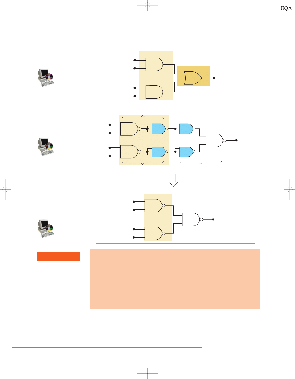
3-13
ALTERNATE LOGIC-GATE REPRESENTATIONS
We have introduced the five basic logic gates (AND, OR, INVERTER, NAND,
and NOR) and the standard symbols used to represent them on logic-circuit
diagrams. Although you may find that some circuit diagrams still use these
86
C
HAPTER
3/
D
ESCRIBING
L
OGIC
C
IRCUITS
C
D
A
B
74LS00
74LS00
(8)
x
(9)
74LS00
(10)
(3)
(6)
(1)
(2)
(4)
(5)
(c)
(b)
C
D
A
B
74LS08
74LS08
(3)
x = AB + CD
(1)
(2)
(3)
(6)
(1)
(2)
(4)
(5)
C
D
A
B
x
74LS32
AND
OR
AND
After eliminating
double inversions
7
(a)
1
2
3
5
4
6
FIGURE 3-32
Possible
implementations for
Example 3-18.
REVIEW QUESTIONS
1. How many different ways do we now have to implement the inversion op-
eration in a logic circuit?
2. Implement the expression
x
(A B)(C D) using OR and AND gates.
Then implement the expression using only NOR gates by converting
each OR and AND gate to its NOR implementation from Figure 3-30.
Which circuit is more efficient?
3. Write the output expression for the circuit of Figure 3-32(c), and use
DeMorgan’s theorems to show that it is equivalent to the expression for
the circuit of Figure 3-32(a).
TOCCMC03_0131725793.QXD 12/2/05 8:18 PM Page 86
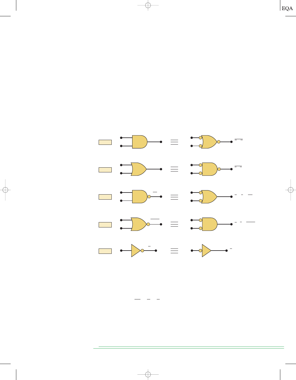
standard symbols exclusively, it has become increasingly more common to
find circuit diagrams that utilize alternate logic symbols
in addition to the
standard symbols.
Before discussing the reasons for using an alternate symbol for a logic
gate, we will present the alternate symbols for each gate and show that they
are equivalent to the standard symbols. Refer to Figure 3-33; the left side of
the illustration shows the standard symbol for each logic gate, and the right
side shows the alternate symbol. The alternate symbol for each gate is ob-
tained from the standard symbol by doing the following:
1. Invert each input and output of the standard symbol. This is done by
adding bubbles (small circles) on input and output lines that do not have
bubbles and by removing bubbles that are already there.
2. Change the operation symbol from AND to OR, or from OR to AND. (In
the special case of the INVERTER, the operation symbol is not changed.)
S
ECTION
3-13/
A
LTERNATE
L
OGIC
-G
ATE
R
EPRESENTATIONS
87
FIGURE 3-33
Standard
and alternate symbols for
various logic gates and
inverter.
A
B
A
B
A
B
A
B
A
B
A
B
A
B
A
B
A
A
A
•
B
A + B
AB
A + B
A
A
A
•
B = A + B
A + B = AB
A + B = AB
A
•
B = A + B
AND
OR
NAND
NOR
INV
For example, the standard NAND symbol is an AND symbol with a bub-
ble on its output. Following the steps outlined above, remove the bubble
from the output, and add a bubble to each input. Then change the AND sym-
bol to an OR symbol. The result is an OR symbol with bubbles on its inputs.
We can easily prove that this alternate symbol is equivalent to the stan-
dard symbol by using DeMorgan’s theorems and recalling that the bubble
represents an inversion operation. The output expression from the standard
NAND symbol is
which is the same as the output expression for
the alternate symbol. This same procedure can be followed for each pair of
symbols in Figure 3-33.
Several points should be stressed regarding the logic symbol equivalences:
1. The equivalences can be extended to gates with
any number of inputs.
2. None of the standard symbols have bubbles on their inputs, and all the
alternate symbols do.
AB = A + B,
TOCCMC03_0131725793.QXD 12/2/05 8:18 PM Page 87
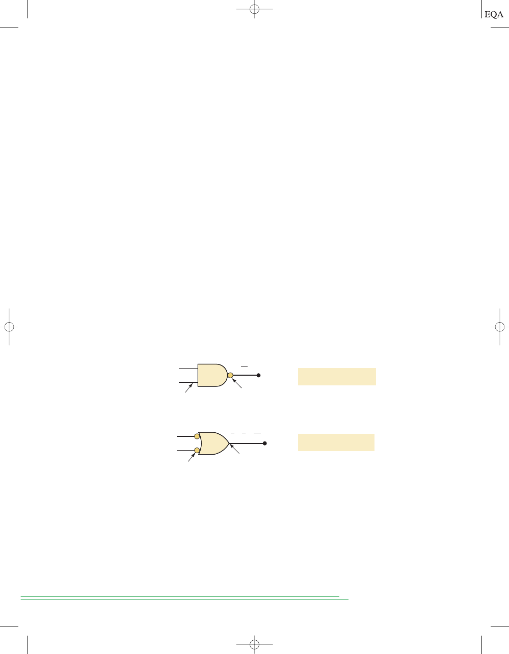
3. The standard and alternate symbols for each gate represent the same
physical circuit;
there is no difference in the circuits represented by the two
symbols.
4. NAND and NOR gates are inverting gates, and so both the standard and
the alternate symbols for each will have a bubble on
either the input or
the output. AND and OR gates are
noninverting gates, and so the alter-
nate symbols for each will have bubbles on
both inputs and output.
Logic-Symbol Interpretation
Each of the logic-gate symbols of Figure 3-33 provides a unique interpreta-
tion of how the gate operates. Before we can demonstrate these interpreta-
tions, we must first establish the concept of active logic levels.
When an input or output line on a logic circuit symbol has
no bubble on
it, that line is said to be active-HIGH. When an input or output line
does have
a
bubble on it, that line is said to be active-LOW. The presence or absence of
a bubble, then, determines the active-HIGH/active-LOW status of a circuit’s
inputs and output, and is used to interpret the circuit operation.
To illustrate, Figure 3-34(a) shows the standard symbol for a NAND gate.
The standard symbol has a bubble on its output and no bubbles on its inputs.
Thus, it has an active-LOW output and active-HIGH inputs. The logic opera-
tion represented by this symbol can therefore be interpreted as follows:
The output goes LOW only when all of the inputs are HIGH.
Note that this says that the output will go to its active state only when
all of
the inputs are in their active states. The word
all is used because of the AND
symbol.
88
C
HAPTER
3/
D
ESCRIBING
L
OGIC
C
IRCUITS
FIGURE 3-34
Interpretation of the two
NAND gate symbols.
A
B
AB
A
B
Active -HIGH
LOW state is
the active state.
(a)
Output goes LOW only
when all inputs are HIGH.
Active -LOW
HIGH state is the
active state.
(b)
Output is HIGH when
any input is LOW.
A + B = AB
The alternate symbol for a NAND gate shown in Figure 3-34(b) has an
active-HIGH output and active-LOW inputs, and so its operation can be stated
as follows:
The output goes HIGH when any input is LOW.
This says that the output will be in its active state whenever
any of the in-
puts is in its active state. The word
any is used because of the OR symbol.
With a little thought, you can see that the two interpretations for the
NAND symbols in Figure 3-34 are different ways of saying the same thing.
TOCCMC03_0131725793.QXD 12/2/05 8:18 PM Page 88
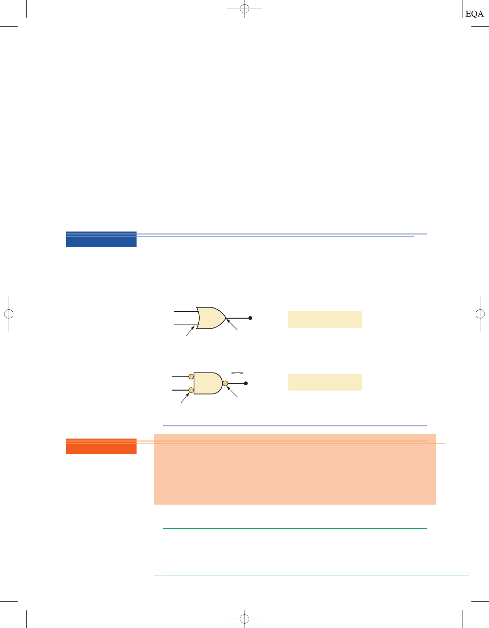
Summary
At this point you are probably wondering why there is a need to have two dif-
ferent symbols and interpretations for each logic gate. We hope the reasons
will become clear after reading the next section. For now, let us summarize
the important points concerning the logic-gate representations.
1. To obtain the alternate symbol for a logic gate, take the standard symbol
and change its operation symbol (OR to AND, or AND to OR), and change
the bubbles on both inputs and output (i.e., delete bubbles that are pres-
ent, and add bubbles where there are none).
2. To interpret the logic-gate operation, first note which logic state, 0 or 1,
is the active state for the inputs and which is the active state for the out-
put. Then realize that the output’s active state is produced by having
all
of the inputs in their active state (if an AND symbol is used) or by having
any of the inputs in its active state (if an OR symbol is used).
S
ECTION
3-14/
W
HICH
G
ATE
R
EPRESENTATION TO
U
SE
89
FIGURE 3-35
Interpretation of the two
OR gate symbols.
Give the interpretation of the two OR gate symbols.
Solution
The results are shown in Figure 3-35. Note that the word
any is used when the
operation symbol is an OR symbol and the word
all is used when it includes
an AND symbol.
A
B
A
•
B = A + B
A
B
A + B
Active-HIGH
HIGH state is
active state.
(a)
Output goes HIGH when
any input is HIGH.
Output goes LOW only
when all inputs are LOW.
Active-LOW
LOW state is
active state.
(b)
3-14
WHICH GATE REPRESENTATION TO USE
Some logic-circuit designers and some textbooks use only the standard logic-
gate symbols in their circuit schematics. While this practice is not incorrect, it
does nothing to make the circuit operation easier to follow. Proper use of the
alternate gate symbols in the circuit diagram can make the circuit operation
EXAMPLE 3-19
REVIEW QUESTIONS
1. Write the interpretation of the operation performed by the standard
NOR gate symbol in Figure 3-33.
2. Repeat question 1 for the alternate NOR gate symbol.
3. Repeat question 1 for the alternate AND gate symbol.
4. Repeat question 1 for the standard AND gate symbol.
TOCCMC03_0131725793.QXD 12/2/05 8:18 PM Page 89
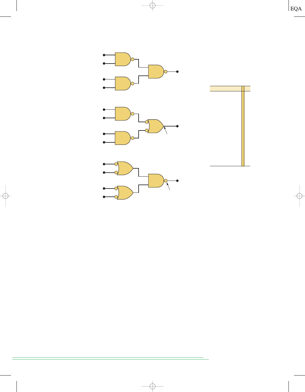
much clearer. This can be illustrated by considering the example shown in
Figure 3-36.
The circuit in Figure 3-36(a) contains three NAND gates connected to
produce an output
Z that depends on inputs A, B, C, and D. The circuit dia-
gram uses the standard symbol for each of the NAND gates. While this dia-
gram is logically correct, it does not facilitate an understanding of how the
circuit functions. The circuit representations given in Figures 3-36(b) and (c),
however, can be analyzed more easily to determine the circuit operation.
The representation of Figure 3-36(b) is obtained from the original circuit
diagram by replacing NAND gate 3 with its alternate symbol. In this dia-
gram, output
Z is taken from a NAND gate symbol that has an active-HIGH
output. Thus, we can say that
Z will go HIGH when either X or Y is LOW. Now,
since
X and Y each appear at the output of NAND symbols having active-LOW
outputs, we can say that
X will go LOW only if A
B 1, and Y will go LOW
only if
C
D 1. Putting this all together, we can describe the circuit oper-
ation as follows:
Output Z will go HIGH whenever either A
B 1 or C D 1
(or both).
This description can be translated to truth-table form by setting
Z
1 for
those cases where
A
B 1 and for those cases where C D 1. For all other
cases,
Z is made a 0. The resultant truth table is shown in Figure 3-36(d).
The representation of Figure 3-36(c) is obtained from the original circuit
diagram by replacing NAND gates 1 and 2 by their alternate symbols. In this
90
C
HAPTER
3/
D
ESCRIBING
L
OGIC
C
IRCUITS
FIGURE 3-36
(a) Original
circuit using standard
NAND symbols; (b) equiva-
lent representation where
output
Z is active-HIGH; (c)
equivalent representation
where output
Z is active-
LOW; (d) truth table.
(d )
A
0
0
0
0
0
0
0
0
1
1
1
1
1
1
1
1
B
0
0
0
0
1
1
1
1
0
0
0
0
1
1
1
1
C
0
0
1
1
0
0
1
1
0
0
1
1
0
0
1
1
D
0
1
0
1
0
1
0
1
0
1
0
1
0
1
0
1
Z
0
0
0
1
0
0
0
1
0
0
0
1
1
1
1
1
A
B
Z
C
D
A
B
C
D
A
B
C
D
1
2
3
(a)
(b)
(c)
1
2
Z
X
Y
Active-HIGH
Z
Active-LOW
X
Y
3
3
1
2
TOCCMC03_0131725793.QXD 12/2/05 8:18 PM Page 90
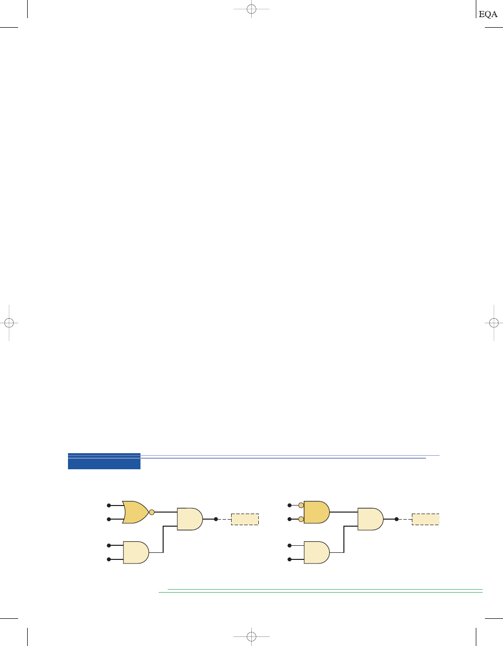
equivalent representation, the
Z output is taken from a NAND gate that has an
active-LOW output. Thus, we can say that
Z will go LOW only when X
Y 1.
Because
X and Y are active-HIGH outputs, we can say that X will be HIGH
when either
A or B is LOW, and Y will be HIGH when either C or D is LOW.
Putting this all together, we can describe the circuit operation as follows:
Output Z will go LOW only when A or B is LOW and C or D is LOW.
This description can be translated to truth-table form by making
Z
0 for all
cases where at least one of the
A or B inputs is LOW at the same time that at
least one of the
C or D inputs is LOW. For all other cases, Z is made a 1. The
resultant truth table is the same as that obtained for the circuit diagram of
Figure 3-36(b).
Which Circuit Diagram Should Be Used?
The answer to this question depends on the particular function being per-
formed by the circuit output. If the circuit is being used to cause some action
(e.g., turn on an LED or activate another logic circuit) when output
Z goes to
the 1 state, then we say that
Z is to be active-HIGH, and the circuit diagram
of Figure 3-36(b) should be used. On the other hand, if the circuit is being
used to cause some action when
Z goes to the 0 state, then Z is to be active-
LOW, and the diagram of Figure 3-36(c) should be used.
Of course, there will be situations where
both output states are used to
produce different actions and either one can be considered to be the active
state. For these cases, either circuit representation can be used.
Bubble Placement
Refer to the circuit representation of Figure 3-36(b) and note that the symbols
for NAND gates 1 and 2 were chosen to have active-LOW outputs to match the
active-LOW inputs of NAND gate 3. Refer to the circuit representation of
Figure 3-36(c) and note that the symbols for NAND gates 1 and 2 were chosen
to have active-HIGH outputs to match the active-HIGH inputs of NAND gate 3.
This leads to the following general rule for preparing logic-circuit schematics:
Whenever possible, choose gate symbols so that bubble outputs are
connected to bubble inputs, and nonbubble outputs to nonbubble
inputs.
The following examples will show how this rule can be applied.
S
ECTION
3-14/
W
HICH
G
ATE
R
EPRESENTATION TO
U
SE
91
A
B
C
D
2
1
Z
A
B
C
D
2
1
Z
(a)
(b)
ALARM
ALARM
FIGURE 3-37
Example 3-20.
EXAMPLE 3-20
The logic circuit in Figure 3-37(a) is being used to activate an alarm when its
output
Z goes HIGH. Modify the circuit diagram so that it represents the cir-
cuit operation more effectively.
TOCCMC03_0131725793.QXD 12/2/05 8:18 PM Page 91

Solution
Because
Z
1 will activate the alarm, Z is to be active-HIGH. Thus, the AND
gate 2 symbol does not have to be changed. The NOR gate symbol should be
changed to the alternate symbol with a nonbubble (active-HIGH) output to
match the nonbubble input of AND gate 2, as shown in Figure 3-37(b). Note
that the circuit now has nonbubble outputs connected to the nonbubble in-
puts of gate 2.
92
C
HAPTER
3/
D
ESCRIBING
L
OGIC
C
IRCUITS
FIGURE 3-38
Example 3-21.
When the output of the logic circuit in Figure 3-38(a) goes LOW, it activates
another logic circuit. Modify the circuit diagram to represent the circuit op-
eration more effectively.
E
D
C
B
A
1
2
Z
(b)
E
D
C
B
A
Z
(a)
1
2
Solution
Because
Z is to be active-LOW, the symbol for OR gate 2 must be changed to
its alternate symbol, as shown in Figure 3-38(b). The new OR gate 2 symbol
has bubble inputs, and so the AND gate and OR gate 1 symbols must be
changed to bubbled outputs, as shown in Figure 3-38(b). The INVERTER al-
ready has a bubble output. Now the circuit has all bubble outputs connected
to bubble inputs of gate 2.
Analyzing Circuits
When a logic-circuit schematic is drawn using the rules we followed in these
examples, it is much easier for an engineer or technician (or student) to fol-
low the signal flow through the circuit and to determine the input conditions
that are needed to activate the output. This will be illustrated in the follow-
ing examples—which, incidentally, use circuit diagrams taken from the logic
schematics of an actual microcomputer.
The logic circuit in Figure 3-39 generates an output,
MEM, that is used to ac-
tivate the memory ICs in a particular microcomputer. Determine the input
conditions necessary to activate
MEM.
EXAMPLE 3-21
EXAMPLE 3-22
TOCCMC03_0131725793.QXD 12/2/05 8:18 PM Page 92
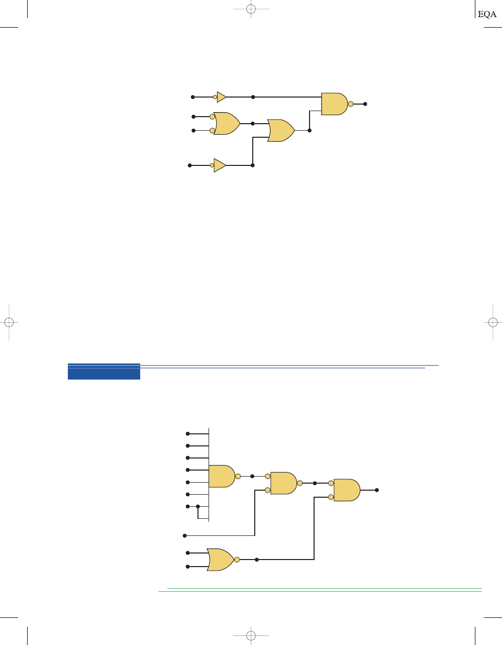
Solution
One way to do this would be to write the expression for
MEM in terms of the
inputs
RD, ROM-A, ROM-B, and RAM, and to evaluate it for the 16 possible
combinations of these inputs. While this method would work, it would re-
quire a lot more work than is necessary.
A more efficient method is to interpret the circuit diagram using the
ideas we have been developing in the last two sections. These are the steps:
1.
MEM is active-LOW, and it will go LOW only when X and Y are HIGH.
2.
X will be HIGH only when RD
0.
3.
Y will be HIGH when either W or V is HIGH.
4.
V will be HIGH when RAM
0.
5.
W will be HIGH when either ROM-A or ROM-B
0.
6. Putting this all together,
MEM will go LOW only when RD
0 and at
least one of the three inputs
ROM-A, ROM-B, or RAM is LOW.
S
ECTION
3-14/
W
HICH
G
ATE
R
EPRESENTATION TO
U
SE
93
FIGURE 3-39
Example 3-22.
FIGURE 3-40
Example 3-23.
MEM
Y
X
V
W
RD
ROM-A
ROM-B
RAM
The logic circuit in Figure 3-40 is used to control the drive spindle motor for
a floppy disk drive when the microcomputer is sending data to or receiving
data from the disk. The circuit will turn on the motor when
DRIVE
1.
Determine the input conditions necessary to turn on the motor.
EXAMPLE 3-23
Note: All gates are CMOS
DRIVE
Y
W
74HC30
74HC32
74HC02
A
1
A
2
A
3
A
4
A
5
A
6
A
7
IN
OUT
A
0
X
74HC02
TOCCMC03_0131725793.QXD 12/2/05 8:18 PM Page 93

Solution
Once again, we will interpret the diagram in a step-by-step fashion:
1.
DRIVE is active-HIGH, and it will go HIGH only when X
Y 0.
2.
X will be LOW when either IN or OUT is HIGH.
3.
Y will be LOW only when W
0 and A
0
0.
4.
W will be LOW only when A
1
through
A
7
are all HIGH.
5. Putting this all together,
DRIVE will be HIGH when A
1
A
2
A
3
A
4
A
5
A
6
A
7
1 and A
0
0, and either IN or OUT or both are 1.
Note the strange symbol for the eight-input CMOS NAND gate (74HC30);
also note that signal
A
7
is connected to two of the NAND inputs.
Asserted Levels
We have been describing logic signals as being active-LOW or active-HIGH.
For example, the output
MEM in Figure 3-39 is active-LOW, and the output
DRIVE in Figure 3-40 is active-HIGH because these are the output states that
cause something to happen. Similarly, Figure 3-40 has active-HIGH inputs
A
1
to
A
7
, and active-LOW input
A
0
.
When a logic signal is in its active state, it can be said to be asserted. For
example, when we say that input
A
0
is asserted, we are saying that it is in its
active-LOW state. When a logic signal is not in its active state, it is said to be
unasserted. Thus, when we say that
DRIVE is unasserted, we mean that it is
in its inactive state (low).
Clearly, the terms
asserted and unasserted are synonymous with active
and
inactive, respectively:
asserted
active
unasserted
inactive
Both sets of terms are in common use in the digital field, so you should rec-
ognize both ways of describing a logic signal’s active state.
Labeling Active-LOW Logic Signals
It has become common practice to use an overbar to label active-LOW sig-
nals. The overbar serves as another indication that the signal is active-LOW;
of course, the absence of an overbar means that the signal is active-HIGH.
To illustrate, all of the signals in Figure 3-39 are active-LOW, and so they
can be labeled as follows:
,
,
,
,
Remember, the overbar is simply a way to emphasize that these are active-
LOW signals. We will employ this convention for labeling logic signals when-
ever appropriate.
Labeling Bistate Signals
Very often, an output signal will have two active states; that is, it will have
one important function in the HIGH state and another in the LOW state. It
is customary to label such signals so that both active states are apparent. A
common example is the read/write signal,
which is interpreted as
follows: when this signal is HIGH, the read operation (
RD) is performed;
when it is LOW, the write operation (
WR) is performed.
RD/WR,
MEM
RAM
ROM-B
ROM-A
RD
94
C
HAPTER
3/
D
ESCRIBING
L
OGIC
C
IRCUITS
TOCCMC03_0131725793.QXD 12/2/05 8:18 PM Page 94
S
ECTION
3-15/
IEEE/ANSI S
TANDARD
L
OGIC
S
YMBOLS
95
REVIEW QUESTIONS
1. Use the method of Examples 3-22 and 3-23 to determine the input con-
ditions needed to activate the output of the circuit in Figure 3-37(b).
2. Repeat question 1 for the circuit of Figure 3-38(b).
3. How many NAND gates are shown in Figure 3-39?
4. How many NOR gates are shown in Figure 3-40?
5. What will be the output level in Figure 3-38(b) when all of the inputs are
asserted?
6. What inputs are required to assert the alarm output in Figure 3-37(b)?
7. Which of the following signals is active-LOW:
?
RD,
W,
R/W
3-15
IEEE/ANSI STANDARD LOGIC SYMBOLS
The logic symbols we have used so far in this chapter are the
traditional stan-
dard symbols used in the digital industry for many, many years. These tradi-
tional symbols use a distinctive shape for each logic gate. A newer standard
for logic symbols was developed in 1984; it is called the IEEE/ANSI Standard
91-1984 for logic symbols. The IEEE/ANSI standard uses rectangular symbols
to represent all logic gates and circuits. A special
dependency notation inside
the rectangular symbol indicates how the device outputs depend on the de-
vice inputs. Figure 3-41 shows the IEEE/ANSI symbols alongside the tradi-
tional symbols for the basic logic gates. Note the following points:
1. The rectangular symbols use a small right triangle (
) in place of the
small bubble of the traditional symbols to indicate the inversion of the
logic level. The presence or absence of the triangle also signifies whether
an input or output is active-LOW or active-HIGH.
x
x
x
x
x
A
B
A
B
A
B
A
B
A
A
B
A
B
A
B
A
B
A
x
x
x
x
x
(b)
(a)
NOR
NAND
OR
AND
NOT
1
&
&
≥1
≥1
FIGURE 3-41
Standard
logic symbols: (a) traditional;
(b) IEEE/ANSI.
TOCCMC03_0131725793.QXD 12/2/05 8:18 PM Page 95

2. A special notation inside each rectangular symbol describes the logic re-
lation between inputs and output. The “1” inside the INVERTER symbol
denotes a device with only
one input; the triangle on the output indicates
that the output will go to its active-LOW state when that one input is in
its active-HIGH state. The “&” inside the AND symbol means that the
output will go to its active-HIGH state when all of the inputs are in their
active-HIGH state. The “ ” inside the OR gate means that the output
will go to its active state (HIGH) whenever
one or more inputs are in their
active state (HIGH).
3. The rectangular symbols for the NAND and the NOR are the same as
those for the AND and the OR, respectively, with the addition of the
small inversion triangle on the output.
Traditional or IEEE/ANSI?
The IEEE/ANSI standard has not yet been widely accepted for use in the dig-
ital field, although you will run across it in some newer equipment schemat-
ics. Most digital IC data books include both the traditional and IEEE/ANSI
symbols, and it is possible that the newer standard might eventually become
more widely used. We will employ the traditional symbols in most of the cir-
cuit diagrams throughout this book.
Ú
96
C
HAPTER
3/
D
ESCRIBING
L
OGIC
C
IRCUITS
REVIEW QUESTIONS
1. Draw all of the basic logic gates using both the traditional symbols and
the IEEE/ANSI symbols.
2. Draw the IEEE/ANSI symbol for a NOR gate with active-HIGH output.
3-16
SUMMARY OF METHODS TO DESCRIBE LOGIC CIRCUITS
The topics we have covered so far in this chapter have all centered around
just three simple logic functions that we refer to as AND, OR, and NOT. The
concept is not new to anyone because we all use these logical functions every
day as we make decisions. Here are some logical examples. If it is raining OR
the newspaper says that it could rain, then I will take my umbrella. If I get
my paycheck today AND I make it to the bank, then I will have money to
spend this evening. If I have a passing grade in lecture AND I have NOT
failed in lab, then I will pass my digital class. At this point, you may be won-
dering why we have spent so much effort in describing such familiar con-
cepts. The answer can be summed up in two key points:
1. We must be able to represent these logical decisions.
2. We must be able to combine these logic functions and implement a decision-
making system.
We have learned how to represent each of the basic logic functions using:
Logical statements in our own language
Truth tables
Traditional graphic logic symbols
TOCCMC03_0131725793.QXD 12/2/05 8:18 PM Page 96
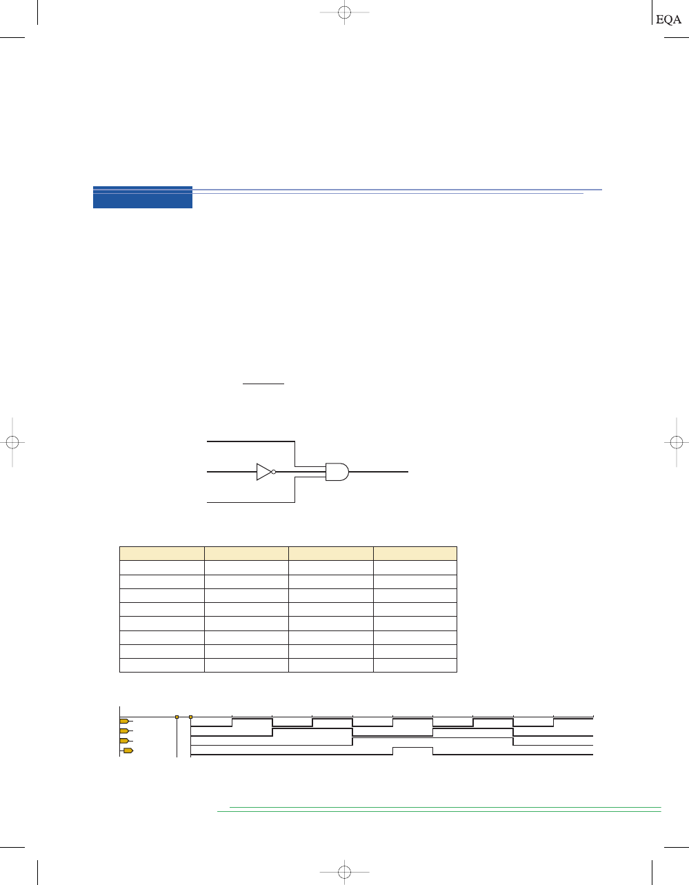
IEEE/ANSI standard logic symbols
Boolean algebra expressions
Timing diagrams
S
ECTION
3-16/
S
UMMARY OF
M
ETHODS TO
D
ESCRIBE
L
OGIC
C
IRCUITS
97
The following English expression describes the way a logic circuit needs to
operate in order to drive a seatbelt warning indicator in a car.
If the driver is present AND the driver is NOT buckled up AND
the ignition switch is on, THEN turn on the warning light.
Describe the circuit using Boolean algebra, schematic diagrams with logic
symbols, truth tables, and timing diagrams.
Solution
See Figure 3-42.
EXAMPLE 3-24
Boolean expression
warning_light = driver_present • buckled_up • ignition_on
(a)
Schematic diagram
driver_present
buckled_up
ignition_on
(b)
Truth table
driver_present
0
0
0
0
1
1
1
1
buckled_up
0
0
1
1
0
0
1
1
ignition_on
0
1
0
1
0
1
0
1
warning_light
0
0
0
0
0
1
0
0
(c)
Timing diagram
Name
ignition_on
buckled_up
driver_present
warning_light
0
0
1
0
Val
1.0 ms
2.0 ms
3.0 ms
4.0 ms
5.0 ms
6.0 ms
7.0 ms
8.0 ms
9.0 ms
10 ms
(d)
warning_light
FIGURE 3-42
Methods of describing logic circuits: (a) Boolean expression;
(b) schematic diagram; (c) truth table; (d) timing diagram.
TOCCMC03_0131725793.QXD 12/2/05 8:18 PM Page 97

Figure 3-42 shows four different ways of representing the logic circuit
that was described in English as the problem statement of Example 3-24.
There are many other ways in which we could represent the logic of this de-
cision. As an example we could dream up an entirely new set of graphic sym-
bols, or state the logical relationship in French or Japanese. Of course, we
cannot cover all the possible ways of describing a logic circuit, but we must
understand the most common methods to be able to communicate with oth-
ers in this profession. Furthermore, certain situations are easier to describe
using one method over another. In some cases, a picture is worth a thousand
words, and in other cases words are concise enough and are more easily com-
municated to others. The important point here is that we need ways to de-
scribe and communicate the operation of digital systems.
98
C
HAPTER
3/
D
ESCRIBING
L
OGIC
C
IRCUITS
REVIEW QUESTION
1. Name five ways to describe the operation of logic circuits.
3-17
DESCRIPTION LANGUAGES VERSUS PROGRAMMING
LANGUAGES*
Recent trends in the field of digital systems are favoring text-based language
description of digital circuits. You probably noticed that each description
method in Figure 3-42 offers challenges to computer entry, whether it is due to
overbars, symbols, formatting, or line-drawing issues. In this section, we will
begin to learn some of the more advanced tools that professionals in the digi-
tal field use to describe the circuits that implement their ideas. These tools are
referred to as hardware description languages (HDLs). Even with the powerful
computers we have today, it is not possible to describe a logic circuit in English
prose and expect the computer to understand what you mean. Computers need
a more rigidly defined language. We will focus on two languages in this text:
Altera hardware description language (AHDL) and very high speed integrated
circuit (VHSIC) hardware description language (VHDL).
VHDL and AHDL
VHDL is not a new language. It was developed by the Department of
Defense in the early 1980s as a concise way to document the designs in the
very high speed integrated circuit (VHSIC) program. Appending HDL onto
this acronym was too much, even for the military, and so the language was ab-
breviated to VHDL. Computer programs were developed to take the VHDL
language files and simulate the operation of the circuits. With the growth of
complex programmable logic devices in digital systems, VHDL has evolved
into one of the primary high-level hardware description languages for de-
signing and implementing digital circuits (synthesis). The language has been
standardized by the IEEE, making it universally appealing for engineers as
well as the makers of software tools that translate designs into the bit pat-
terns used to program actual devices.
AHDL is a language that the Altera Corporation developed to provide a
convenient way to configure the logic devices that they offer. Altera was one
of the first companies to introduce logic devices that can be reconfigured
*All sections covering hardware description languages may by skipped without loss of continuity in the
balance of Chapters 1–12.
TOCCMC03_0131725793.QXD 12/2/05 8:18 PM Page 98

electronically. These devices are called programmable logic devices (PLDs).
Unlike VHDL, this language is not intended to be used as a universal lan-
guage for describing any logic circuit. It is intended to be used for program-
ming complex digital systems into Altera PLDs in a language that is generally
perceived to be easier to learn yet very similar to VHDL. It also has features
that take full advantage of the architecture of Altera devices. All of the ex-
amples in this text will use the Altera MAX
PLUS II or Quartus II software
to develop both AHDL and VHDL design files. You will see the advantage of
using Altera’s development system for both languages when you program an
actual device. The Altera system makes circuit development very easy and
contains all the necessary tools to translate from the HDL design file to a file
ready to load into an Altera PLD. It also allows you to develop building
blocks using schematic entry, AHDL, VHDL, and other methods and then in-
terconnect them to form a complete system.
Other HDLs are available that are more suitable for programming simple
programmable logic devices. You will find any of these languages easy to use
after learning the basics of AHDL or VHDL as covered in this text.
Computer Programming Languages
It is important to distinguish between hardware description languages in-
tended to describe the hardware configuration of a circuit and programming
languages that represent a sequence of instructions intended to be carried
out by a computer to accomplish some task. In both cases, we use a
language
to
program a device. However, computers are complex digital systems that
are made up of logic circuits. Computers operate by following a laundry list
of tasks (i.e., instructions, or “the program”), each of which must be done in
sequential order. The speed of operation is determined by how fast the com-
puter can execute each instruction. For example, if a computer were to respond
to four different inputs, it would require at least four separate instructions
(sequential tasks) to detect and identify which input changed state. A digi-
tal logic circuit, on the other hand, is limited in its speed only by how quickly
the circuitry can change the outputs in response to changes in the inputs. It
is monitoring all inputs concurrently (at the same time) and responding to
any changes.
The following analogy will help you understand the difference between
computer operation and digital logic circuit operation and the role of lan-
guage elements used to describe what the systems do. Consider the chal-
lenge of describing what is done to an Indy 500 car during a pit stop. If a single
person performed all the necessary tasks one at a time, he or she would need
to be very fast at each task. This is the way a computer operates: one task at
a time but very quickly. Of course, at Indy, there is an entire pit crew that
swarms the car, and each member of the crew does his or her task while the
others do theirs. All crew members operate concurrently, like the elements
of a digital circuit. Now consider how you would describe to someone else
what is being done to the Indy car during the pit stop using (1) the individual-
mechanic approach or (2) the pit-crew approach. Wouldn’t the two English
language descriptions of what is being done sound very similar? As we will
see, the languages used to describe digital hardware (HDL) are very similar
to languages that describe computer programs (e.g., BASIC, C, JAVA), even
though the resulting implementation operates quite differently. Knowledge
of any of these computer programming languages is not necessary to under-
stand HDL. The important thing is that when you have learned both an HDL
and a computer language, you must understand their different roles in digi-
tal systems.
S
ECTION
3-17/
D
ESCRIPTION
L
ANGUAGES
V
ERSUS
P
ROGRAMMING
L
ANGUAGES
99
TOCCMC03_0131725793.QXD 12/2/05 8:18 PM Page 99
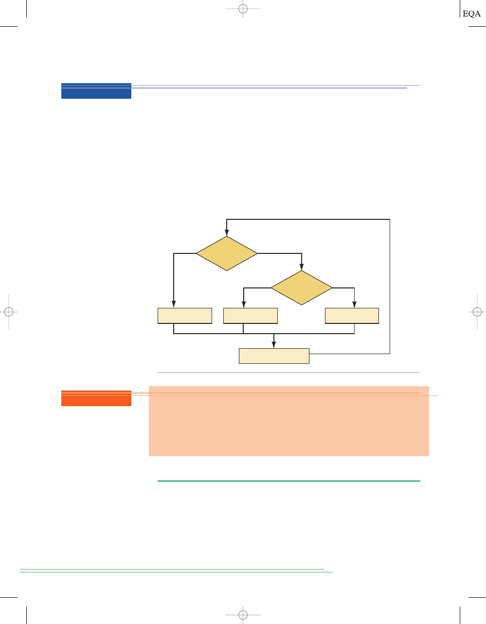
3-18
IMPLEMENTING LOGIC CIRCUITS WITH PLDs
Many digital circuits today are implemented using programmable logic de-
vices (PLDs). These devices are not like microcomputers or microcontrollers
that “run” the program of instructions. Instead, they are configured elec-
tronically, and their internal circuits are “wired” together electronically to
form a logic circuit. This programmable wiring can be thought of as thou-
sands of connections that are either connected (1) or not connected (0).
Figure 3-44 shows a small area of programmable connections. Each intersec-
tion between a row (horizontal wire) and a column (vertical wire) is a pro-
grammable connection. You can imagine how difficult it would be to try to
100
C
HAPTER
3/
D
ESCRIBING
L
OGIC
C
IRCUITS
FIGURE 3-43
Decision
process of a computer
program.
Compare the operation of a computer and a logic circuit in performing the
simple logical operation of
y
AB.
Solution
The logic circuit is a simple AND gate. The output
y will be HIGH within ap-
proximately 10 nanoseconds of the point when
A and B are HIGH simultane-
ously. Within approximately 10 nanoseconds after either input goes LOW,
the output
y will be LOW.
The computer must run a program of instructions that makes decisions.
Suppose each instruction takes 20 ns (that’s pretty fast!). Each shape in the
flowchart shown in Figure 3-43 represents one instruction. Clearly, it will
take a minimum of two or three instructions (40–60 ns) to respond to
changes in the inputs.
EXAMPLE 3-25
REVIEW QUESTIONS
1. What does HDL stand for?
2. What is the purpose of an HDL?
3. What is the purpose of a computer programming language?
4. What is the key difference between HDL and computer programming
languages?
Jump back and repeat
Make y LOW
Make y LOW
Make y HIGH
Is B HIGH?
Is A HIGH?
No
Yes
No
Yes
TOCCMC03_0131725793.QXD 12/2/05 8:18 PM Page 100
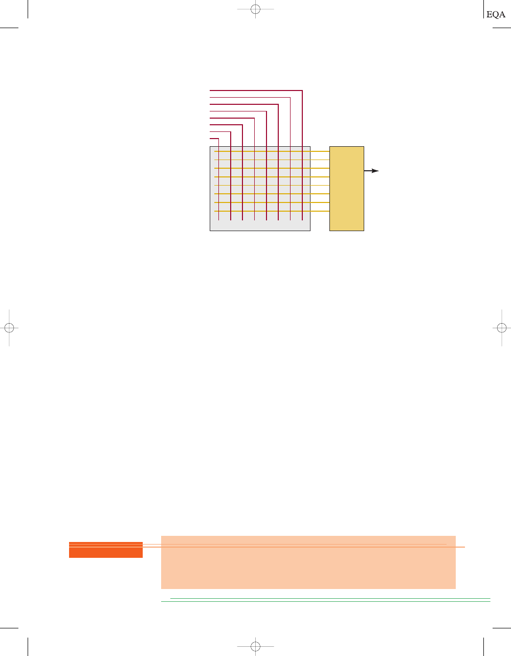
S
ECTION
3-18/
I
MPLEMENTING
L
OGIC
C
IRCUITS WITH
PLD
S
101
FIGURE 3-44
Configuring
hardware connections with
programmable logic
devices.
configure these devices by placing 1s and 0s in a grid manually (which is how
they did it back in the 1970s).
The role of the hardware description language is to provide a concise and
convenient way for the designer to describe the operation of the circuit in a
format that a personal computer can handle and store conveniently. The
computer runs a special software application called a compiler to translate
from the hardware description language into the grid of 1s and 0s that can
be loaded into the PLD. If a person can master the higher-level hardware de-
scription language, it actually makes programming the PLDs much easier
than trying to use Boolean algebra, schematic drawings, or truth tables. In
much the same way that you learned the English language, we will start by
expressing simple things and gradually learn the more complicated aspects
of these languages. Our objective is to learn enough of HDL to be able to
communicate with others and perform simple tasks. A full understanding of
all the details of these languages is beyond the scope of this text and can re-
ally be mastered only by regular use.
In the sections throughout this book that cover the HDLs, we will present
both AHDL and VHDL in a format that allows you to skip over one language
and concentrate on the other without missing important information. Of
course, this setup means there will be some redundant information presented
if you choose to read about both languages. We feel this redundancy is worth
the extra effort to provide you with the flexibility of focusing on either of the
two languages or learning both by comparing and contrasting similar exam-
ples. The recommended way to use the text is to focus on one language. It is
true that the easiest way to become bilingual, and fluent in both languages, is
to be raised in an environment where both languages are spoken routinely. It
is also very easy, however, to confuse details, so we will keep the specific ex-
amples separate and independent. We hope this format provides you with the
opportunity to learn one language now and then use this book as a reference
later in your career should you need to pick up the second language.
A
B
C
D
E
F
G
H
Programmable connections matrix
Logic
circuits
Digital
INPUTS
REVIEW QUESTIONS
1. What does PLD stand for?
2. How are the circuits reconfigured electronically in a PLD?
3. What does a compiler do?
TOCCMC03_0131725793.QXD 12/2/05 8:18 PM Page 101
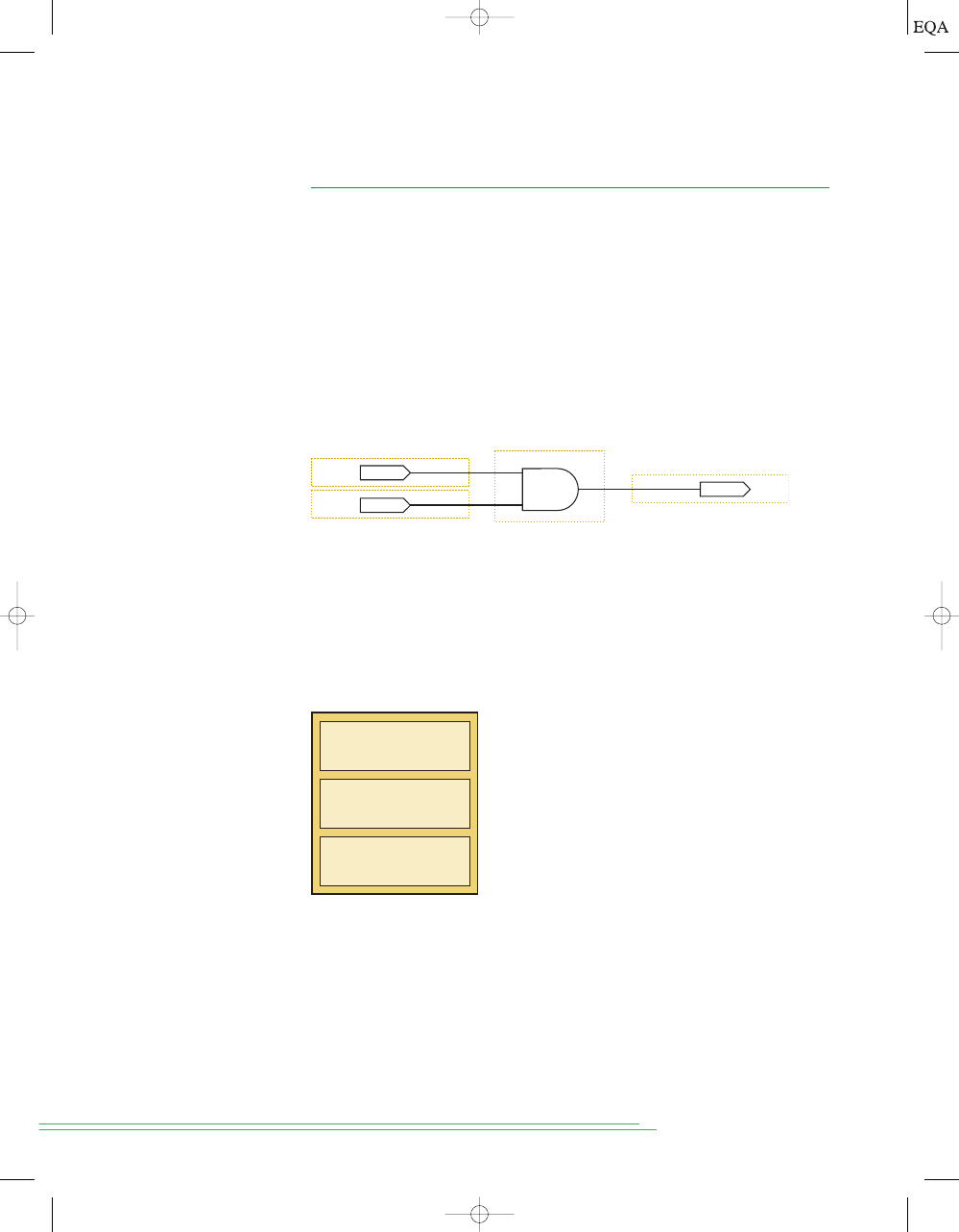
102
C
HAPTER
3/
D
ESCRIBING
L
OGIC
C
IRCUITS
3-19
HDL FORMAT AND SYNTAX
Any language has its unique properties, similarities to other languages, and
its proper syntax. When we study grammar in school, we learn conventions
such as the order of words as elements in a sentence and proper punctuation.
This is referred to as the syntax of language. A language designed to be in-
terpreted by a computer must follow strict rules of syntax. A computer is just
an assortment of processed beach sand and wire that has no idea what you
“meant” to say, so you must present the instructions using the exact syntax
that the computer language expects and understands. The basic format of any
hardware circuit description (in any language) involves two vital elements:
1. The definition of what goes into it and what comes out of it (i.e.,
input/output specs)
2. The definition of how the outputs respond to the inputs (i.e., its operation)
A circuit schematic diagram such as Figure 3-45 can be read and under-
stood by a competent engineer or technician because both would under-
stand the meaning of each symbol in the drawing. If you understand how
each element works and how the elements are connected to each other, you
can understand how the circuit operates. On the left side of the diagram is
the set of inputs, and on the right is the set of outputs. The symbols in the
middle define its operation. The text-based language must convey the same
information. All HDLs use the format shown in Figure 3-46.
FIGURE 3-45
A schematic
diagram description.
FIGURE 3-46
Format of
HDL files.
y
OUTPUT
a
INPUT
b
AND2
INPUT
Functional description
I/O definitions
Documentation
In a text-based language, the circuit being described must be given a
name. The inputs and outputs (sometimes called ports) must be assigned
names and defined according to the nature of the port. Is it a single bit from
a toggle switch? Or is it a four-bit number coming from a keypad? The text-
based language must somehow convey the nature of these inputs and out-
puts. The mode of a port defines whether it is input, output, or both. The type
refers to the number of bits and how those bits are grouped and interpreted.
If the
type of input is a single bit, then it can have only two possible values:
0 and 1. If the type of input is a four-bit binary number from a keypad, it can
have any one of 16 different values
The type determines
the range of possible values. The definition of the circuit’s operation in a
(0000
2
-
1111
2
).
TOCCMC03_0131725793.QXD 12/2/05 8:18 PM Page 102
S
ECTION
3-19/
HDL F
ORMAT AND
S
YNTAX
103
FIGURE 3-47
Essential
elements in AHDL.
SUBDESIGN and_gate
(
a, b
:INPUT;
y
:OUTPUT;
)
BEGIN
y
a & b;
END;
The SUBDESIGN section defines the inputs and outputs of the logic cir-
cuit block. Something must enclose the circuit that we are trying to describe,
much the same way that a block diagram encloses everything that makes up
that part of the design. In AHDL, this input/output definition is enclosed in
parentheses. The list of variables used for inputs to this block are separated
by commas and followed by :INPUT;. In AHDL, the single-bit type is assumed
unless the variable is designated as multiple bits. The single-output bit is de-
clared with the mode :OUTPUT;. We will learn the proper way to describe
other types of inputs, outputs, and variables as we need to use them.
The set of statements that describe the operation of the AHDL circuit
are contained in the logic section between the keywords BEGIN and END. In
this example, the operation of the hardware is described by a very simple
Boolean algebra equation that states that the output (
y) is assigned (
) the
logic level produced by
a AND b. This Boolean algebra equation is referred
to as a concurrent assignment statement. Any statements (there is only one
in this example) between BEGIN and END are evaluated constantly and con-
currently. The order in which they are listed makes no difference. The basic
Boolean operators are:
&
AND
#
OR
!
NOT
$
XOR
REVIEW QUESTIONS
1. What appears inside the parentheses ( ) after SUBDESIGN?
2. What appears between BEGIN and END?
AHDL
text-based language is contained in a set of statements that follow the circuit in-
put/output (I/O) definition. The following two sections describe the very simple
circuit of Figure 3-45 and illustrate the critical elements of AHDL and VHDL.
BOOLEAN DESCRIPTION USING AHDL
Refer to Figure 3-47. The keyword SUBDESIGN gives a name to the circuit
block, which in this case is
and_gate. The name of the file must also be
and_gate.tdf. Notice that the keyword SUBDESIGN is capitalized. This is not
required by the software, but use of a consistent style in capitalization makes
the code much easier to read. The style guide that is provided with the Altera
compiler for AHDL suggests the use of capital letters for the keywords in the
language. Variables that are named by the designer should be lowercase.
TOCCMC03_0131725793.QXD 12/2/05 8:18 PM Page 103
BOOLEAN DESCRIPTION USING VHDL
Refer to Figure 3-48. The keyword ENTITY gives a name to the circuit block,
which in this case is and_gate. Notice that the keyword ENTITY is capital-
ized but and_gate is not. This is not required by the software, but use of a
consistent style in capitalization makes the code much easier to read. The
style guide provided with the Altera compiler for VHDL suggests using cap-
ital letters for the keywords in the language.Variables that are named by the
designer should be lowercase.
104
C
HAPTER
3/
D
ESCRIBING
L
OGIC
C
IRCUITS
FIGURE 3-48
Essential
elements in VHDL.
REVIEW QUESTIONS
1. What is the role of the ENTITY declaration?
2. Which key section defines the operation of the circuit?
3. What is the assignment operator used to give a value to a logic signal?
ENTITY and_gate IS
PORT ( a, b :IN BIT;
y :OUT BIT);
END and_gate;
ARCHITECTURE ckt OF and_gate IS
BEGIN
y <= a AND b;
END ckt;
The ENTITY declaration can be thought of as a block description.
Something must enclose the circuit we are trying to describe, much the same
way a block diagram encloses everything that makes up that part of the de-
sign. In VHDL, the keyword PORT tells the compiler that we are defining in-
puts and outputs to this circuit block. The names used for inputs (separated
by commas) are listed, ending with a colon and a description of the mode and
type of input (:IN BIT;). In VHDL, the BIT description tells the compiler that
each variable in the list is a single bit. We will learn the proper way to de-
scribe other types of inputs, outputs, and variables as we need to use them.
The line containing END and_gate; terminates the ENTITY declaration.
The ARCHITECTURE declaration is used to describe the operation of
everything inside the block. The designer makes up a name for this architec-
tural description of the inner workings of the ENTITY block (
ckt in this ex-
ample). Every ENTITY must have at least one ARCHITECTURE associated
with it. The words OF and IS are keywords in this declaration. The body of
the architecture description is enclosed between the BEGIN and END key-
words. END is followed by the name that has been assigned to this architec-
ture. Within the body (between BEGIN and END) is the description of the
block’s operation. In this example, the operation of the hardware is de-
scribed by a very simple Boolean algebra equation that states that the out-
put (
y) is assigned (
) the logic level produced by
a AND b. This is referred
to as a concurrent assignment statement, which means that all the state-
ments (there is only one in this example) between BEGIN and END are eval-
uated constantly and concurrently. The order in which they are listed makes
no difference.
6 =
VHDL
TOCCMC03_0131725793.QXD 12/2/05 8:18 PM Page 104
3-20
INTERMEDIATE SIGNALS
In many designs, there is a need to define signal points “inside” the circuit
block. They are points in the circuit that are neither inputs nor outputs for
the block but may be useful as a reference point. It may be a signal that
needs to be connected to many other places within the block. In an analog or
digital schematic diagram, they would be called test points or
nodes. In an
HDL, they are referred to as buried nodes or local signals. Figure 3-49 shows
a very simple circuit that uses an intermediate signal named
m. In the HDL,
these nodes (signals) are not defined with the inputs and outputs but rather
in the section that describes the operation of the block. The inputs and out-
puts are available to other circuit blocks in the system, but these local sig-
nals are recognized only within this block.
S
ECTION
3-20/
I
NTERMEDIATE
S
IGNALS
105
FIGURE 3-49
A logic circuit diagram with an intermediate variable.
a
INPUT
b
y
OUTPUT
c
m
Intermediate signal m
INPUT
INPUT
In the example code that follows, notice the information at the top. The
purpose of this information is strictly for documentation purposes. It is ab-
solutely vital that the design is documented thoroughly. At a minimum, it
should describe the project it is being used in, who wrote it, and the date.
This information is often referred to as a header. We are keeping our head-
ers brief to make this book a little lighter to carry to class, but remember:
memory space is cheap and information is valuable. So don’t be afraid to
document thoroughly! There are also comments next to many of the state-
ments in the code. These comments help the designer remember what she or
he was trying to do and to help any other person to understand what was in-
tended.
AHDL BURIED NODES
The AHDL code that describes the circuit in Figure 3-49 is shown in Figure
3-50. The comments in AHDL can be enclosed between % characters, as you
can see in the figure between lines 1 and 4. This section of the code allows
the designer to write many lines of information that will be ignored by com-
puter programs using this file but can be read by any person trying to deci-
pher the code. Notice that the comments at the end of lines 9, 10, 13, 15, and
16 are preceded by two dashes (--). The text following the dashes is for docu-
mentation only. Either type of comment symbol may be used, but percent
signs must be used in pairs to open and close a comment. Double dashes in-
dicate a comment that extends to the end of the line.
In AHDL, local signals are declared in the VARIABLE section, which is
placed between the SUBDESIGN section and the logic section. The interme-
diate signal
m is defined on line 11, following the keyword VARIABLE. The
AHDL
TOCCMC03_0131725793.QXD 12/5/05 10:06 PM Page 105
keyword NODE designates the nature of the variable. Notice that a colon
separates the variable name from its node designation. In the hardware de-
scription on line 13, the intermediate variable is assigned (connected to) a
value
and then m is used in the second statement on line 14 to
assign (connect) a value to
y
Remember that the assignment
statements are concurrent and, thus, the order in which they are given does
not matter. For human readability, it may seem more logical to assign values
to intermediate variables before they are used in other assignment state-
ments, as shown here.
(
y = m # c;).
(
m = a & b;)
106
C
HAPTER
3/
D
ESCRIBING
L
OGIC
C
IRCUITS
FIGURE 3-50
Intermediate variables
in AHDL described in
Figure 3-49.
1 % Intermediate variables in AHDL (Figure 3-49)
2 Digital Systems 10th ed
3 NS Widmer
4 MAY 23, 2005 %
5 SUBDESIGN fig3_50
6 (
7 a,b,c :INPUT; -- define inputs to block
8 y :OUTPUT; -- define block output
9 )
10 VARIABLE
11 m :NODE; -- name an intermediate signal
12 BEGIN
13 m
a & b; -- generate buried product term
14 y
m # c; -- generate sum on output
15 END;
REVIEW QUESTIONS
1. What is the designation used for intermediate variables?
2. Where are these variables declared?
3. Does it matter whether the
m or y equation comes first?
4. What character is used to limit a block of comments?
5. What characters are used to comment a single line?
VHDL LOCAL SIGNALS
The VHDL code that describes the circuit in Figure 3-49 is shown in Figure
3-51. The comments in VHDL follow two dashes (--). Typing two successive
dashes allows the designer to write information from that point to the end of
the line. The information following the two successive dashes will be ignored
by computer programs using this file, but can be read by any person trying to
decipher the code.
The intermediate signal
m is defined on line 13 following the keyword
SIGNAL. The keyword BIT designates the type of the signal. Notice that a
colon separates the signal name from its type designation. In the hardware de-
scription on line 16, the intermediate signal is assigned (connected to) a value
VHDL
TOCCMC03_0131725793.QXD 12/2/05 8:18 PM Page 106

and then
m is used in the statement on line 17 to assign (con-
nect) a value to
y
Remember that the assignment statements
are concurrent and, thus, the order in which they are given does not matter.
For human readability, it may seem more logical to assign values to interme-
diate signals before they are used in other assignment statements, as shown
here.
(
y
6 =
m
OR
c;).
(
m
6 =
a
AND
b;)
S
UMMARY
107
1 -- Intermediate variables in VHDL (Figure 3-49)
2 -- Digital Systems 10th ed
3 -- NS Widmer
4 -- MAY 23, 2005
5
6 ENTITY fig3_51 IS
7 PORT( a, b, c :IN BIT; -- define inputs to block
8 y :OUT BIT); -- define block output
9 END fig3_51;
10
11 ARCHITECTURE ckt OF fig3_51 IS
12
13 SIGNAL m :BIT; -- name an intermediate signal
14
15 BEGIN
16 m <= a AND b; -- generate buried product term
17 y <= m OR c; -- generate sum on output
18 END ckt;
REVIEW QUESTIONS
1. What is the designation used for intermediate signals?
2. Where are these signals declared?
3. Does it matter whether the m or y equation comes first?
4. What characters are used to comment a single line?
SUMMARY
1. Boolean algebra is a mathematical tool used in the analysis and design of
digital circuits.
2. The basic Boolean operations are the OR, AND, and NOT operations.
3. An OR gate produces a HIGH output when any input is HIGH. An AND
gate produces a HIGH output only when all inputs are HIGH. A NOT cir-
cuit (INVERTER) produces an output that is the opposite logic level
compared to the input.
4. A NOR gate is the same as an OR gate with its output connected to an IN-
VERTER. A NAND gate is the same as an AND gate with its output con-
nected to an INVERTER.
FIGURE 3-51
Intermediate signals in VHDL described in Figure 3-49.
TOCCMC03_0131725793.QXD 12/2/05 8:19 PM Page 107

5. Boolean theorems and rules can be used to simplify the expression of a
logic circuit and can lead to a simpler way of implementing the circuit.
6. NAND gates can be used to implement any of the basic Boolean opera-
tions. NOR gates can be used likewise.
7. Either standard or alternate symbols can be used for each logic gate, de-
pending on whether the output is to be active-HIGH or active-LOW.
8. The IEEE/ANSI standard for logic symbols uses rectangular symbols for
each logic device, with special notations inside the rectangles to show
how the outputs depend on the inputs.
9. Hardware description languages have become an important method of
describing digital circuits.
10. HDL code should always contain comments that document its vital char-
acteristics so a person reading it later can understand what it does.
11. Every HDL circuit description contains a definition of the inputs and
outputs, followed by a section that describes the circuit’s operation.
12. In addition to inputs and outputs, intermediate connections that are
buried within the circuit can be defined. These intermediate connec-
tions are called nodes or signals.
108
C
HAPTER
3/
D
ESCRIBING
L
OGIC
C
IRCUITS
logic level
Boolean algebra
truth table
OR operation
OR gate
AND operation
AND gate
NOT operation
inversion
(complementation)
NOT circuit
(INVERTER)
NOR gate
NAND gate
Boolean theorems
DeMorgan’s theorems
alternate logic
symbols
active logic levels
active-HIGH
active-LOW
asserted
unasserted
IEEE/ANSI
hardware description
languages (HDLs)
Altera hardware
description
language (AHDL)
very high speed
integrated circuit
(VHSIC) hardware
description
language (VHDL)
programmable logic
devices (PLDs)
concurrent
compiler
syntax
mode
type
SUBDESIGN
concurrent
assignment
statement
ENTITY
BIT
ARCHITECTURE
buried nodes (local
signals)
comments
VARIABLE
NODE
IMPORTANT TERMS
PROBLEMS
The color letters preceding some of the problems are used to indicate the na-
ture or type of problem as follows:
B
basic problem
T
troubleshooting problem
D
design or circuit-modification problem
N
new concept or technique not covered in text
C
challenging problem
H
HDL problem
TOCCMC03_0131725793.QXD 12/2/05 8:19 PM Page 108
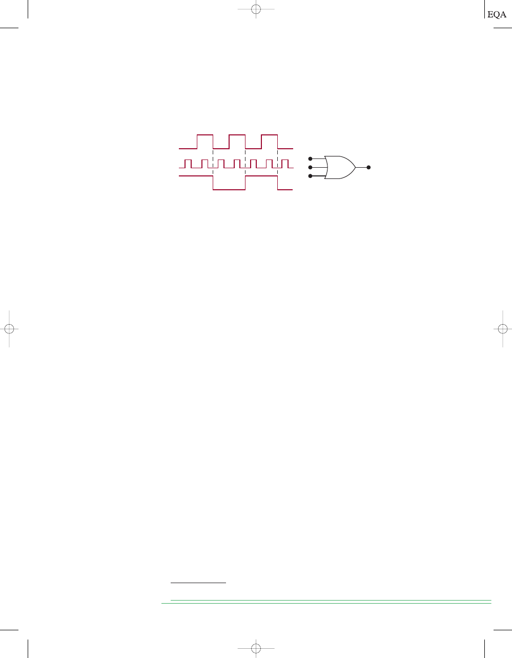
SECTION 3-3
3-1.*Draw the output waveform for the OR gate of Figure 3-52.
P
ROBLEMS
109
*Answers to problems marked with an asterisk can be found in the back of the text.
FIGURE 3-52
A
B
C
x
A
B
C
3-2. Suppose that the
A input in Figure 3-52 is unintentionally shorted to
ground (i.e.,
A
0). Draw the resulting output waveform.
3-3.*Suppose that the
A input in Figure 3-52 is unintentionally shorted
to the
5 V supply line (i.e., A 1). Draw the resulting output wave-
form.
3-4. Read the statements below concerning an OR gate. At first, they may
appear to be valid, but after some thought you should realize that nei-
ther one is
always true. Prove this by showing a specific example to re-
fute each statement.
(a) If the output waveform from an OR gate is the same as the wave-
form at one of its inputs, the other input is being held perma-
nently LOW.
(b) If the output waveform from an OR gate is always HIGH, one of its
inputs is being held permanently HIGH.
3-5. How many different sets of input conditions will produce a HIGH out-
put from a five-input OR gate?
SECTION 3-4
3-6. Change the OR gate in Figure 3-52 to an AND gate.
(a)*Draw the output waveform.
(b) Draw the output waveform if the
A input is permanently shorted
to ground.
(c) Draw the output waveform if
A is permanently shorted to
5 V.
3-7.*Refer to Figure 3-4. Modify the circuit so that the alarm is to be acti-
vated only when the pressure and the temperature exceed their max-
imum limits at the same time.
3-8.*Change the OR gate in Figure 3-6 to an AND gate and draw the output
waveform.
3-9. Suppose that you have an unknown two-input gate that is either an
OR gate or an AND gate. What combination of input levels should you
apply to the gate’s inputs to determine which type of gate it is?
3-10.
True or false: No matter how many inputs it has, an AND gate will pro-
duce a HIGH output for only one combination of input levels.
B
B
C
B
B
D
B
B
B
B
TOCCMC03_0131725793.QXD 12/2/05 8:19 PM Page 109
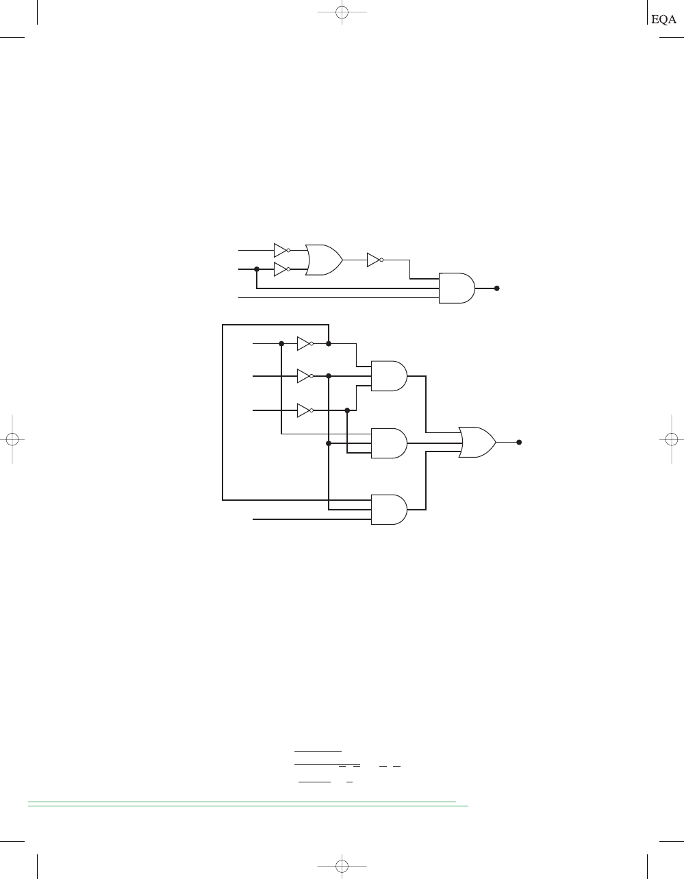
SECTIONS 3-5 TO 3-7
3-11. Apply the
A waveform from Figure 3-23 to the input of an INVERTER.
Draw the output waveform. Repeat for waveform
B.
3-12. (a)* Write the Boolean expression for output
x in Figure 3-53(a).
Determine the value of
x for all possible input conditions, and
list the values in a truth table.
(b) Repeat for the circuit in Figure 3-53(b).
110
C
HAPTER
3/
D
ESCRIBING
L
OGIC
C
IRCUITS
FIGURE 3-53
A
(a)
x
B
C
(b)
A
B
C
D
x
3-13.*Create a complete analysis table for the circuit of Figure 3-15(b) by
finding the logic levels present at each gate output for each of the 32
possible input combinations.
3-14. (a)*Change each OR to an AND, and each AND to an OR, in Figure
3-15(b). Then write the expression for the output.
(b) Complete an analysis table.
3-15. Create a complete analysis table for the circuit of Figure 3-16 by find-
ing the logic levels present at each gate output for each of the 16 pos-
sible combinations of input levels.
SECTION 3-8
3-16. For each of the following expressions, construct the corresponding
logic circuit, using AND and OR gates and INVERTERs.
(a)*
(b)*
(c)
y = (M + N + PQ)
z = A + B + CDE) + BCD
x = AB(C + D)
B
B
B
B
B
B
TOCCMC03_0131725793.QXD 12/2/05 8:19 PM Page 110
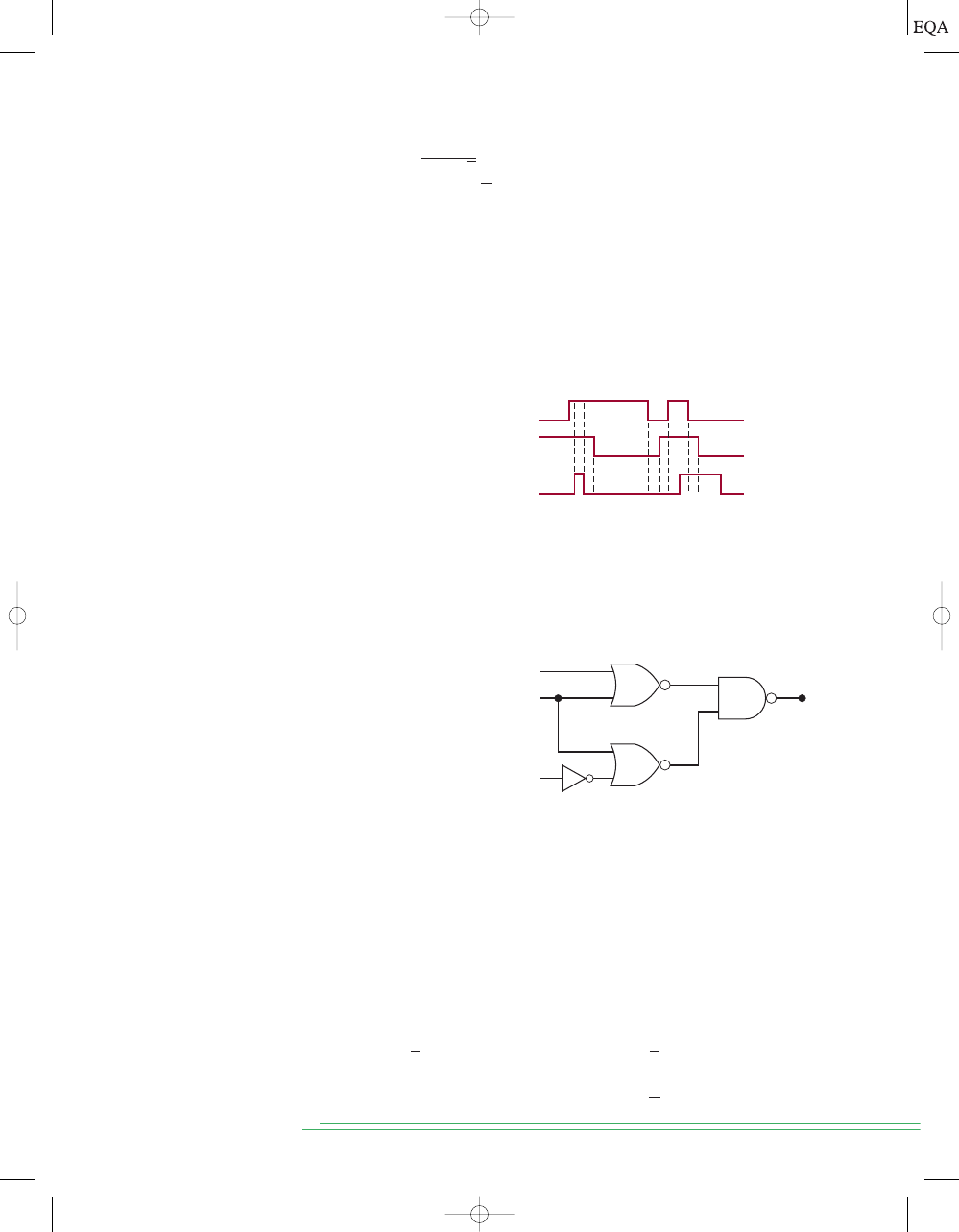
(d)
(e)
(f)
SECTION 3-9
3-17.*(a) Apply the input waveforms of Figure 3-54 to a NOR gate, and draw
the output waveform.
(b) Repeat with
C held permanently LOW.
(c) Repeat with
C held HIGH.
x = (A + B) (A + B)
z = MN(P + N )
x = W + PQ
P
ROBLEMS
111
FIGURE 3-54
A
B
C
3-18. Repeat Problem 3-17 for a NAND gate.
3-19.*Write the expression for the output of Figure 3-55, and use it to de-
termine the complete truth table. Then apply the waveforms of Figure
3-54 to the circuit inputs, and draw the resulting output waveform.
X
A
B
C
FIGURE 3-55
3-20. Determine the truth table for the circuit of Figure 3-24.
3-21. Modify the circuits that were constructed in Problem 3-16 so that
NAND gates and NOR gates are used wherever appropriate.
SECTION 3-10
3-22. Prove theorems (15a) and (15b) by trying all possible cases.
3-23.* DRILL QUESTION
Complete each expression.
(a)
A
1 __________
(f)
__________
(b)
__________
(g)
D
0 __________
(c)
__________
(h)
__________
(d)
C
C __________
(i)
G
GF __________
(e)
__________
(j)
__________
y + wy =
x
#
0 =
C + C =
B
#
B =
A
#
A =
D
#
1 =
B
B
C
B
B
B
C
TOCCMC03_0131725793.QXD 12/2/05 8:19 PM Page 111
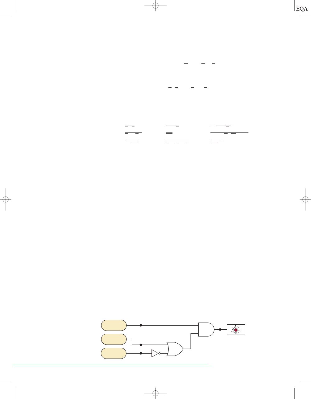
3-24. (a)*Simplify the following expression using theorems (13b), (3), and (4):
)
(b) Simplify the following expression using theorems (13a), (8), and (6):
SECTIONS 3-11 AND 3-12
3-25. Prove DeMorgan’s theorems by trying all possible cases.
3-26. Simplify each of the following expressions using DeMorgan’s theo-
rems.
(a)*
(d)
(g)*
(b)
(e)*
(h)
(c)*
(f)
(i)
3-27.*Use DeMorgan’s theorems to simplify the expression for the output of
Figure 3-55.
3-28. Convert the circuit of Figure 3-53(b) to one using only NAND gates.
Then write the output expression for the new circuit, simplify it using
DeMorgan’s theorems, and compare it with the expression for the
original circuit.
3-29. Convert the circuit of Figure 3-53(a) to one using only NOR gates.
Then write the expression for the new circuit, simplify it using
DeMorgan’s theorems, and compare it with the expression for the
original circuit.
3-30. Show how a two-input NAND gate can be constructed from two-input
NOR gates.
3-31. Show how a two-input NOR gate can be constructed from two-input
NAND gates.
3-32. A jet aircraft employs a system for monitoring the rpm, pressure, and
temperature values of its engines using sensors that operate as follows:
Figure 3-56 shows the logic circuit that controls a cockpit warning
light for certain combinations of engine conditions. Assume that a
HIGH at output
W activates the warning light.
(a)*Determine what engine conditions will give a warning to the pilot.
(b) Change this circuit to one using all NAND gates.
T
sensor
output = 0
only
when
temperature
6
200°F
P
sensor
output = 0
only
when
pressure
6
220
psi
RPM
sensor
output = 0
only
when
speed
6
4800
rpm
ABCD
A + C + D
ABCD
(
M + N )(M + N )
AB
A + BC
A(B + C)D
A + B
ABC
z = ABC + ABC + BCD
x = (M + N )(M + P)(N + P
112
C
HAPTER
3/
D
ESCRIBING
L
OGIC
C
IRCUITS
FIGURE 3-56
Warning
light
W
P
T
R
Temp
sensor
Pressure
sensor
RPM
sensor
C
C
B
B
C
C
B
B
C
TOCCMC03_0131725793.QXD 12/2/05 8:19 PM Page 112
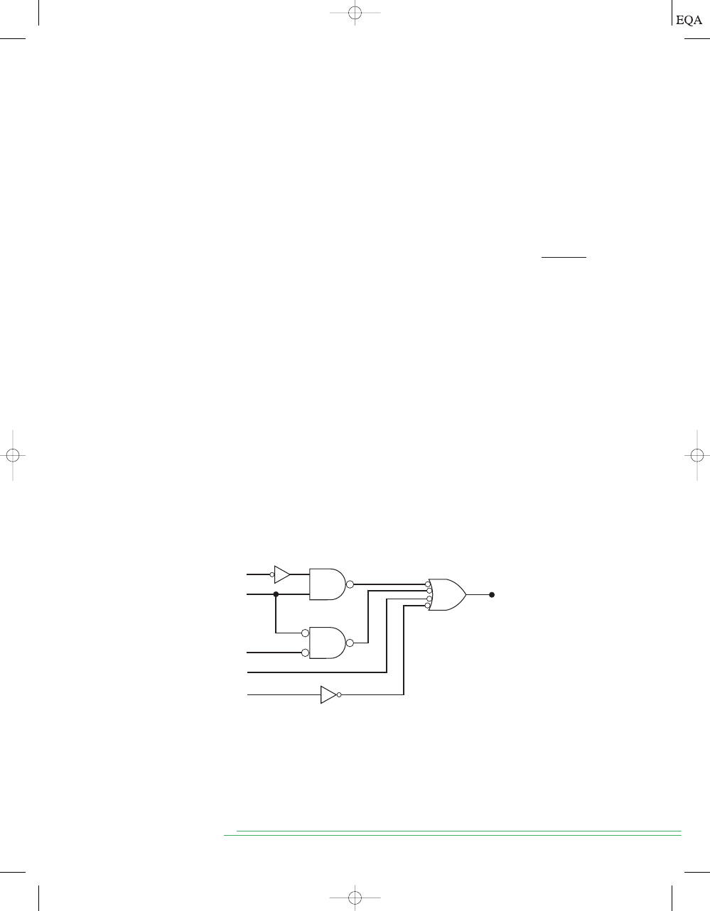
SECTIONS 3-13 AND 3-14
3-33. For each statement below, draw the appropriate logic-gate symbol—
standard or alternate—for the given operation.
(a) A HIGH output occurs only when all three inputs are LOW.
(b) A LOW output occurs when any of the four inputs is LOW.
(c) A LOW output occurs only when all eight inputs are HIGH.
3-34. Draw the standard representations for each of the basic logic gates.
Then draw the alternate representations.
3-35. The circuit of Figure 3-55 is supposed to be a simple digital combina-
tion lock whose output will generate an active-LOW
signal
for only one combination of inputs.
(a)*Modify the circuit diagram so that it represents more effectively
the circuit operation.
(b) Use the new circuit diagram to determine the input combination
that will activate the output. Do this by working back from the
output using the information given by the gate symbols, as was
done in Examples 3-22 and 3-23. Compare the results with the
truth table obtained in Problem 3-19.
3-36. (a) Determine the input conditions needed to activate output
Z in
Figure 3-37(b). Do this by working back from the output, as was
done in Examples 3-22 and 3-23.
(b) Assume that it is the LOW state of
Z that is to activate the alarm.
Change the circuit diagram to reflect this, and then use the re-
vised diagram to determine the input conditions needed to acti-
vate the alarm.
3-37. Modify the circuit of Figure 3-40 so that
A
1
0 is needed to produce
DRIVE
1 instead of A
1
1.
3-38.*Determine the input conditions needed to cause the output in Figure
3-57 to go to its active state.
UNLOCK
P
ROBLEMS
113
FIGURE 3-57
x
A
B
C
D
E
3-39.*What is the asserted state for the output of Figure 3-57? For the out-
put of Figure 3-36(c)?
3-40. Use the results of Problem 3-38 to obtain the complete truth table for
the circuit of Figure 3-57.
3-41.*Figure 3-58 shows an application of logic gates that simulates a two-
way switch like the ones used in our homes to turn a light on or off
B
B
C
C
D
B
B
B
N
TOCCMC03_0131725793.QXD 12/2/05 8:19 PM Page 113
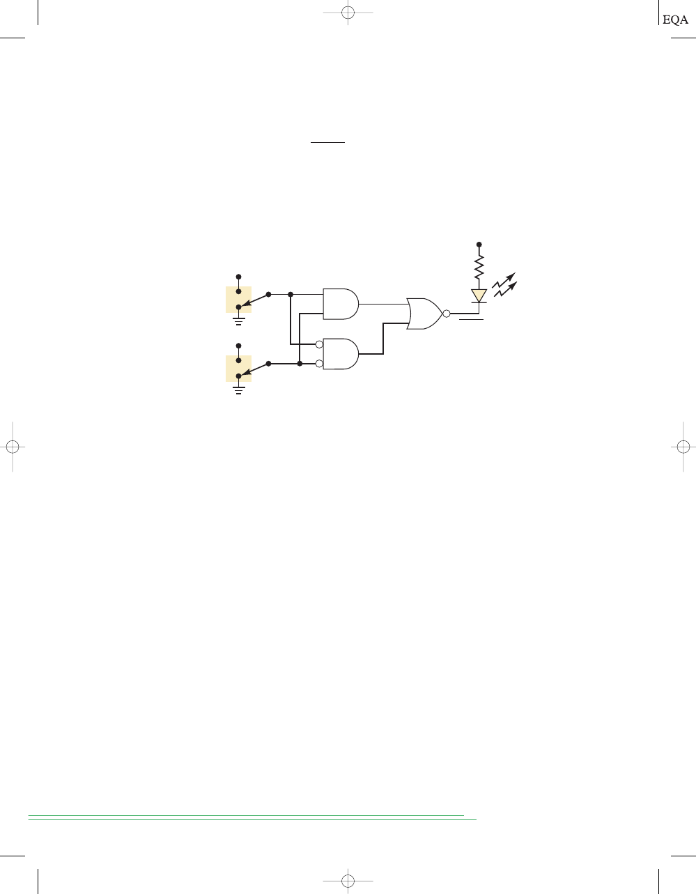
SECTION 3-15
3-42. Redraw the circuits of (a)* Figure 3-57 and (b) Figure 3-58 using the
IEEE/ANSI symbols.
SECTION 3-17
HDL DRILL QUESTIONS
3-43.*
True or false:
(a) VHDL is a computer programming language.
(b) VHDL can accomplish the same thing as AHDL.
(c) AHDL is an IEEE standard language.
(d) Each intersection in a switch matrix can be programmed as an
open or short circuit between a row and column wire.
(e) The first item that appears at the top of an HDL listing is the
functional description.
(f) The type of an object indicates if it is an input or an output.
(g) The mode of an object determines if it is an input or an output.
(h) Buried nodes are nodes that have been deleted and will never be
used again.
(i) Local signals are another name for intermediate variables.
(j) The header is a block of comments that document vital informa-
tion about the project.
SECTION 3-18
3-44. Redraw the programmable connection matrix from Figure 3-44. Label
the output signals (horizontal lines) from the connection matrix (from
114
C
HAPTER
3/
D
ESCRIBING
L
OGIC
C
IRCUITS
FIGURE 3-58
+5 V
LIGHT
+5 V
+5 V
A
B
from two different switches. Here the light is an LED that will be ON
(conducting) when the NOR gate output is LOW. Note that this output
is labeled
to indicate that it is active-LOW. Determine the in-
put conditions needed to turn on the LED. Then verify that the circuit
operates as a two-way switch using switches
A and B. (In Chapter 4,
you will learn how to design circuits like this one to produce a given
relationship between inputs and outputs.)
LIGHT
B
H
B
TOCCMC03_0131725793.QXD 12/2/05 8:19 PM Page 114

top row to bottom row) as follows: AAABADHE. Draw an X in the ap-
propriate intersections to short-circuit a row to a column and create
these connections to the logic circuit.
3-45.*Write the HDL code in the language of your choice that will produce
the following output functions:
X
A B
Y
AB
Z
A B C
3-46. Write the HDL code in the language of your choice that will imple-
ment the logic circuit of Figure 3-39.
(a) Use a single Boolean equation.
(b) Use the intermediate variables
V, W, X, and Y.
MICROCOMPUTER APPLICATION
3-47.*Refer to Figure 3-40 in Example 3-23. Inputs
A
7
through
A
0
are
address
inputs that are supplied to this circuit from outputs of the micro-
processor chip in a microcomputer. The eight-bit address code
A
7
to
A
0
selects which device the microprocessor wants to activate. In Example
3-23, the required address code to activate the disk drive was
A
7
through
A
0
11111110
2
FE
16
.
Modify the circuit so that the microprocessor must supply an ad-
dress code of 4A
16
to activate the disk drive.
CHALLENGING EXERCISES
3-48. Show how
can be implemented with one two-input NOR
and one two-input NAND gate.
3-49.*Implement
y
ABCD using only two-input NAND gates.
ANSWERS TO SECTION REVIEW QUESTIONS
SECTION 3-2
1.
x
1
2.
x
0
3. 32
SECTION 3-3
1. All inputs LOW
2.
x
A B C D E F
3. Constant HIGH
SECTION 3-4
1. All five inputs
1
2. A LOW input will keep the output LOW.
3. False; see
truth table of each gate.
SECTION 3-5
1. Output of second INVERTER will be the same as input
A.
2.
y will be LOW
only for
A
B 1.
SECTION 3-6
1.
2.
x = D(AB + C) + E
x = A + B + C + AD
x
=
ABC
A
NSWERS TO
S
ECTION
R
EVIEW
Q
UESTIONS
115
H
H
C
C
C
TOCCMC03_0131725793.QXD 12/2/05 8:19 PM Page 115

SECTION 3-7
1.
x
1
2.
x
1
3.
x
1 for both.
SECTION 3-8
1. See Figure 3-15(a).
2. See Figure 3-17(b).
3. See Figure 3-15(b).
SECTION 3-9
1. All inputs LOW.
2.
x
0
3.
SECTION 3-10
1.
2.
3.
SECTION 3-11
1.
2.
3. Same as Figure 3-28 except NAND is
replaced by NOR.
4.
SECTION 3-12
1. Three.
2. NOR circuit is more efficient because it can be implemented with
one 74LS02 IC.
3.
SECTION 3-13
1. Output goes LOW when any input is HIGH.
2. Output goes HIGH only when
all inputs are LOW.
3. Output goes LOW when any input is LOW.
4. Output
goes HIGH only when all inputs are HIGH.
SECTION 3-14
1.
Z will go HIGH when A
B 0 and C D 1.
2.
Z will go LOW when
A
B 0, E 1, and either C or D or both are 0.
3. Two
4. Two
5. LOW
6.
A
B 0, C D 1
7.
SECTION 3-15
1. See Figure 3-41.
2. Rectangle with & inside, and triangles on inputs.
SECTION 3-16
1. Boolean equation, truth table, logic diagram, timing diagram, language.
SECTION 3-17
1. Hardware description language
2. To describe a digital circuit and its
operation.
3. To give a computer a sequential list of tasks.
4. HDL describes
concurrent hardware circuits; computer instructions execute one at a time.
SECTION 3-18
1. Programmable logic device
2. By making and breaking connections in a
switching matrix
3. It translates HDL code into a pattern of bits to configure the
switching matix.
SECTION 3-19
AHDL
1. The input and output definitions.
2. The description of how it operates.
W
x = (AB)
(
CD) = AB + (CD) + AB + CD
y = AB(C + D)
y = (R + S + T )Q
z = AB + C
y = AD + BD
y = A
B
D
y = AC
x = A + B + CD
116
C
HAPTER
3/
D
ESCRIBING
L
OGIC
C
IRCUITS
TOCCMC03_0131725793.QXD 12/2/05 8:19 PM Page 116

VHDL
1. To give a name to the circuit and define its inputs and outputs.
2. The
ARCHITECTURE description.
3.
SECTION 3-20
AHDL
1. NODE
2. After the I/O definition and before BEGIN.
3. No
4.
5. --
VHDL
1. SIGNAL
2. Inside ARCHITECTURE before BEGIN.
3. No
4. --
%
6 =
A
NSWERS TO
S
ECTION
R
EVIEW
Q
UESTIONS
117
TOCCMC03_0131725793.QXD 12/2/05 8:19 PM Page 117
Wyszukiwarka
Podobne podstrony:
Digital Systems Chapter06
Digital Systems Chapter02
Digital Systems Chapter01
Digital Systems Chapter13
Digital Systems Chapter10
digital systems
Digital Systems Cover
Digital Systems Glossary
Digital Systems IndexOfICs
Digital Systems Answers
Digital Systems Index
Digital Systems Theoremspdf
Essentials of Management Information Systems 8e Chapter08
Essentials of Management Information Systems 8e Chapter01
Essentials of Management Information Systems 8e Chapter04
Essentials of Management Information Systems 8e Chapter09
Essentials of Management Information Systems 8e Chapter07
więcej podobnych podstron