10-1
Small-Project Management
10-2
Stepper Motor Driver
Project
10-3
Keypad Encoder Project
■
OUTLINE
D I G I T A L S Y S T E M
P R O J E C T S U S I N G H D L
C H A P T E R 1 0
10-4
Digital Clock Project
10-5
Frequency Counter Project
TOCCMC10_0131725793.QXD 12/19/2005 2:13 PM Page 676

677
■
OBJECTIVES
Upon completion of this chapter, you will be able to:
■
Analyze the operation of systems made of several components that
have been covered earlier in this textbook.
■
Describe an entire project with one HDL file.
■
Describe the process of hierarchical project management.
■
Understand how to break a project into manageable pieces.
■
Use
or Quartus II software tools to implement a hierar-
chical modular project.
■
Plan ways to test the operation of the circuits you build.
■
INTRODUCTION
Throughout the first nine chapters of this book, we have explained the fun-
damental building blocks of digital systems. Now that we have taken out
each block and looked it over, we do not want to put them all away and for-
get them; it is time to build something with the blocks. Some of the exam-
ples we have used to demonstrate the operation of individual circuits are
really digital systems in their own right, and we have studied how they
work. In this chapter, we want to focus more on the building process.
Surveys of graduates show us that most of the professionals in the elec-
trical and computer engineering and technology field have the responsibil-
ity of project management. Experience with students has also shown us
that the most efficient way to manage a project is not intuitively obvious to
everyone, which explains why so many of us end up attending the school of
hard knocks (learning through trial and error). This chapter is intended to
give you a strategic plan for managing projects while learning about digital
systems and the modern tools used to develop them. The principles here
are not limited to digital or even electronic projects in general. They could
apply to building a house or building your own business. They will defi-
nitely improve your success rate and reduce the frustration factor.
Hardware description languages were really created for the purpose
of managing large digital systems: for documentation, simulation testing,
and the synthesis of working circuits. Likewise, the Altera software tools
are specifically designed to work with managing projects that go far be-
yond the scope of this text. We will describe some of the features of the
Altera software packages as we go through the steps of developing these
small projects. This concept of modular project development, which was
introduced in Chapter 4, will be demonstrated here through a series of
examples.
MAX + PLUS
II
TOCCMC10_0131725793.QXD 12/19/2005 2:13 PM Page 677
10-1
SMALL-PROJECT MANAGEMENT
The first projects described here are relatively small systems that consist of
a small number of building blocks. These projects can be developed in sep-
arate modules, but this approach would only add to the complexity. They are
small enough that it makes sense to implement the entire project in a sin-
gle HDL design file. This does not mean, however, that a structured process
should
not be followed to complete the project. In fact, most of the same
steps that should be employed in a large modular project are also applica-
ble in these examples. The steps that should be followed are (1) overall def-
inition, (2) strategic planning to break the project into small pieces, (3) syn-
thesis and testing of each piece, and (4) system integration and testing.
Definition
The first step in any project is the thorough definition of its scope. In this
step, the following issues should be determined:
■
How many bits of data are needed?
■
How many devices are controlled by the outputs?
■
What are the names of each input and output?
■
Are the inputs and outputs active-HIGH or active-LOW?
■
What are the speed requirements?
■
Do I understand fully how this device should operate?
■
What will define successful completion of this project?
From this step should come a complete and thorough description of the over-
all project’s operation, a definition of its inputs and outputs, and complete
numeric specifications that define its capabilities and limitations.
Strategic Planning
The second step involves developing a strategy for dividing this overall proj-
ect into manageable pieces. The requirements of the pieces are:
■
A way to test each piece must be developed.
■
Each piece must fit together to make up the whole system.
■
We must know the nature of all the signals that connect the pieces.
■
The exact operation of each block must be thoroughly defined and un-
derstood.
■
We must have a clear vision of how to make each block work.
This last requirement might seem obvious, but it is amazing how many proj-
ects are planned around one central block that involves a not-yet-discovered
technical miracle or violates silly little laws like conservation of energy. In
this stage, each subsystem (section block) becomes somewhat of a project in
and of itself, with the possibility of additional subsystems defined within its
boundaries. This is the concept of hierarchical design.
Synthesis and Testing
Each subsystem should be built starting at the simplest level. In the case of
a digital system designed using HDL, it means writing pieces of code. It also
678
C
HAPTER
10/
D
IGITAL
S
YSTEM
P
ROJECTS
U
SING
HDL
TOCCMC10_0131725793.QXD 12/19/2005 2:13 PM Page 678
means developing a plan for testing that code to make sure it meets all the
criteria. This is often accomplished through some sort of simulation. When a
circuit is simulated on a computer, the designer must create all the different
scenarios that will be experienced by the actual circuit and must also know
what the proper response to those inputs should be. This testing often takes
a great deal of thought and is not an area that should be overlooked. The
worst mistake you can make is to conclude that a fundamental block works
perfectly, only to find later those few situations where it fails. This predica-
ment often forces you to rethink many of the other blocks, thus nullifying
much of your work.
System Integration and Testing
The last step is to put the blocks together and test them as a unit. Blocks are
added and tested at each stage until the entire project is working. This area
is often trivialized but rarely goes smoothly. Even if you took care of all the
details you thought about, there are always the “gotchas” that nobody
thought about.
Some aspects of project planning and management go beyond the scope
of this text. One is the selection of a hardware platform that will best fit your
application. In Chapter 13, we will explore the broad field of digital systems
and look specifically at the capabilities and limitations of PLDs in various
categories. Another very critical dimension in project management is time.
Your boss will give you only a certain amount of time to complete your proj-
ect, and you must plan your work (and effort) to meet this deadline. We will
not be able to cover time management in this text, but as a general rule you
will find that most facets of the project will actually take two to three times
longer than you think they will when you begin.
S
ECTION
10-2/
S
TEPPER
M
OTOR
D
RIVER
P
ROJECT
679
REVIEW QUESTIONS
1. Name the steps of project management.
2. At what stage should you decide how to measure success?
10-2
STEPPER MOTOR DRIVER PROJECT
The purpose of this section is to demonstrate a typical application of coun-
ters combined with decoding circuits. A digital system often contains a
counter that cycles through a specified sequence and whose output states
are decoded by a combinational logic circuit, which in turn controls the op-
eration of the system. Many applications also have external inputs that are
used to put the system into various modes of operation. This section dis-
cusses all these features to control a stepper motor.
In a real project, the first step of definition often involves some research
on the part of the project manager. In this section (or project), it is vital that
we understand what a stepper motor is and how it works before we try to cre-
ate a circuit that is supposed to control it. In Section 7-10, we showed you
how to design a simple synchronous counter that could be used to drive a
stepper motor. The sequence demonstrated in that section is called the
full-
step sequence. As you recall, it involved two flip-flops and their Q and out-
puts driving the four coils of the motor. The full-step sequence always has
two coils of the stepper motor energized in any state of the sequence and
typically causes
of shaft rotation per step. Other sequences, however, will
15°
Q
TOCCMC10_0131725793.QXD 12/19/2005 2:13 PM Page 679
also cause a stepper to rotate. If you look at the full-step sequence, you will
notice that each state transition involves turning off one coil and simultane-
ously turning on another coil. For example, look at the first state (1010) in
the full-step sequence of Table 10-1. When it switches to the second state in
the sequence,
coil 1 is turned off and coil 0 is turned on. The half-step sequence
is created by inserting a state with only one coil energized between full
steps, as shown in the middle column of Table 10-1. In this sequence, one coil
is de-energized before the other is energized. The first state is 1010 and the
second state is 1000, meaning that
coil 1 is turned off for one state before coil
0 is turned on. This intermediate state causes the stepper shaft to rotate half
as far
as it would in the full-step sequence
The half-step se-
quence is used when smaller steps are desirable and more steps per revolu-
tion are acceptable. As it turns out, the stepper motor will rotate in a manner
similar to the full-step sequence (
per step) if you apply only the sequence
of intermediate states with one coil energized at a time. This sequence, called
the
wave-drive sequence, has less torque but operates more smoothly than the
full-step sequence at moderate speeds. The wave-drive sequence is shown in
the right-hand column of Table 10-1.
15°
(15°).
(7.5°)
680
C
HAPTER
10/
D
IGITAL
S
YSTEM
P
ROJECTS
U
SING
HDL
TABLE 10-1
Stepper motor
coil drive sequences.
Full-Step
Half-Step
Wave-Drive
1010
1010
1000
1000
1001
1001
0001
0001
0101
0101
0100
0100
0110
0110
0010
0010
Problem Statement
A microprocessor laboratory needs a universal interface to drive a stepper
motor. In order to experiment with microcontrollers driving stepper motors,
it would be useful to have a single universal interface IC wired to the step-
per motor. This circuit needs to accept any of the typical forms of stepper
drive signals from a microcontroller and activate the windings of the motor
to make it move in the desired manner. The interface needs to operate in one
of four modes: decoded full-step, decoded half-step, decoded wave-drive, or
nondecoded direct drive. The mode is selected by controlling the logic levels
on the
M1, M0 input pins. In the first three modes, the interface receives just
two control bits—a step pulse and a direction control bit—from the micro-
controller. Each time it sees a
rising edge on the step input, the circuit must
cause the motor to move one increment of motion clockwise or counterclock-
wise, depending on the level present on the direction bit. Depending on the
mode that the IC is in, the outputs will respond to each step pulse by chang-
ing state according to the sequences shown in Table 10-1. The fourth mode of
operation of this circuit must allow the microcontroller to control each wind-
ing of the motor directly. In this mode, the circuit accepts four control bits
from the microcontroller and passes these logic levels directly to its outputs,
which are used to energize the stepper coils. The four modes are summarized
in Table 10-2.
TOCCMC10_0131725793.QXD 12/19/2005 2:13 PM Page 680
In modes 0, 1, and 2, the outputs count through the corresponding count
sequence on each rising edge of the step input. The direction input deter-
mines whether the sequence moves forward or backward through the states
in Table 10-1, thus moving the motor clockwise or counterclockwise. From
this description, we can make some decisions about the project.
Inputs
step: rising edge trigger
direction:
backward through table,
forward through table
cin0, cin1, cin2, cin3, m1, m0: active-HIGH control inputs
Outputs
cout0, cout1, cout2, cout3: active-HIGH control outputs
Strategic Planning
This project has two key requirements. It requires a sequential counter cir-
cuit that will control the outputs in three of the modes. In the last mode, the
output does not follow a counter but rather follows the control inputs. While
there are many ways to divide this project and still fulfill these require-
ments, we will choose to have a simple up/down binary counter that responds
to the step and direction inputs. A separate combinational logic circuit will
translate (decode) the binary count into the appropriate output state, de-
pending on the mode input setting. This circuit will also ignore the counter
inputs and pass the control inputs directly to the outputs when the mode is
set to 3. The circuit diagram is shown in Figure 10-1.
Breaking this problem into manageable pieces is also fairly straightfor-
ward. The first step is to build an up/down counter. This counter should be
tested on a simulator using only the direction and step inputs. Next, try to
make each decoded sequence work individually with the counter. Then try
to get the mode inputs to select one of the decoder sequences and add the
direct-drive option (which is fairly trivial). When the circuit can follow the
states shown in Table 10-1 in either direction, for each mode sequence, and
pass the four
cin signals directly to cout in mode 3, we will be successful.
Synthesis and Testing
The code in Figures 10-2 and 10-3 shows the first stage of development: de-
signing and testing an up/down counter. We will use an intermediate integer
variable for the counter value and test it by outputting the count directly to
q. To test this part of the design, we simply need to make sure it can count up
and down through the eight states. Figure 10-4 shows the simulation results.
We only need to provide the clock pulses and make up a direction control sig-
nal, and the simulator demonstrates the counter’s response.
1 =
0 =
S
ECTION
10-2/
S
TEPPER
M
OTOR
D
RIVER
P
ROJECT
681
TABLE 10-2
Mode
M1 M0
Input Signals
Output
0
0
0
Step, direction
Full-step count sequence
1
0
1
Step, direction
Wave-drive count sequence
2
1
0
Step, direction
Half-step count sequence
3
1
1
Four control inputs
Direct drive from control inputs
TOCCMC10_0131725793.QXD 12/19/2005 2:13 PM Page 681
682
C
HAPTER
10/
D
IGITAL
S
YSTEM
P
ROJECTS
U
SING
HDL
Micro-
controller
Direction
Step
Q
0
Q
1
Q
2
Cin3
Cin2
Cin1
Cin0
Cout3
Cout2
Cout1
Cout0
M
+V
Stepper
motor
C
O
U
N
T
E
R
D
E
C
O
D
E
R
D
E
C
O
D
E
R
M1
M0
S1
S0
+5 V
Mode 0, 1, 2
sequencer inputs
Interface
MOD-8 counter
outputs
(no external connection)
Current drivers
(for rated coil current)
Mode control inputs
Mode 3
direct drive inputs
1001
0110
1010
1001
0101
0110
1010
0101
1001
1010
0110
–
0110
0101
1
3
4
5
6
7
0
6
5
4
3
0
7
2
Name:
Value:
1.0 ms
2.0 ms
3.0 ms
4.0 ms
5.0 ms
6.0 ms
7.0 ms
8.0 ms
9.0 ms
10 ms
step
0
dir
0
q[2..0]
H0
Cout[3..0]
B 0010
FIGURE 10-4
Simulation testing of a basic MOD-8.
FIGURE 10-1
A universal stepper motor interface circuit.
FIGURE 10-2
AHDL MOD-8.
FIGURE 10-3
VHDL MOD-8.
SUBDESIGN fig10_2
(
step, dir :INPUT;
q[2..0] :OUTPUT;
)
VARIABLE
count[2..0] : DFF;
BEGIN
count[].clk = step;
IF dir THEN count[].d = count[].q + 1;
ELSE count[].d = count[].q - 1;
END IF;
q[] = count[].q;
END;
ENTITY fig10_3 IS
PORT( step, dir :IN BIT;
q :OUT INTEGER RANGE 0 TO 7);
END fig10_3;
ARCHITECTURE vhdl OF fig10_3 IS
BEGIN
PROCESS (step)
VARIABLE count :INTEGER RANGE 0 TO 7;
BEGIN
IF (step'EVENT AND step = '1') THEN
IF dir = '1' THEN count := count + 1;
ELSE count := count - 1;
END IF;
END IF;
q <= count;
END PROCESS;
END vhdl;
TOCCMC10_0131725793.QXD 12/19/2005 2:13 PM Page 682
The next step is to add one of the decoded outputs and test it, which will
require adding the four-bit
cout output specification. The q output bits of the
MOD-8 counter are kept for the sake of continuity. Figure 10-5 shows the
AHDL code for this stage of testing, and Figure 10-6 shows the VHDL code for
the same stage of testing. Notice that a CASE construct is used to decode the
counter and drive the outputs. In the VHDL code, the
cout outputs have been
declared as bit_vector type because we now want to assign binary bit pat-
terns to them. Figure 10-7 shows the simulated test of its operation with
enough clock cycles included to test an entire counter cycle up and down.
The other count sequences are simply variations of the code we just
tested. It is probably not necessary to test each one independently, so now is
a good time to bring in the mode selector inputs (
m) and direct-drive coil
control inputs (
cin). Notice that the new inputs have been defined in Figures
10-8 (AHDL) and 10-9 (VHDL). Because the mode control has four possible
states and we want to do something different for each state, another CASE
construct works best. In other words, we have chosen to use a CASE structure
to select the mode and a CASE structure within each mode to select the
S
ECTION
10-2/
S
TEPPER
M
OTOR
D
RIVER
P
ROJECT
683
FIGURE 10-5
AHDL full-step sequence decoder.
SUBDESIGN fig10_5
(
step, dir :INPUT;
q[2..0] :OUTPUT;
cout[3..0] :OUTPUT;
)
VARIABLE
count[2..0] : DFF;
BEGIN
count[].clk = step;
IF dir THEN count[].d = count[].q + 1;
ELSE count[].d = count[].q - 1;
END IF;
q[] = count[].q;
CASE count[] IS
WHEN B"000" => cout[] = B"1010";
WHEN B"001" => cout[] = B"1001";
WHEN B"010" => cout[] = B"0101";
WHEN B"011" => cout[] = B"0110";
WHEN B"100" => cout[] = B"1010";
WHEN B"101" => cout[] = B"1001";
WHEN B"110" => cout[] = B"0101";
WHEN B"111" => cout[] = B"0110";
END CASE;
END;
FIGURE 10-6
VHDL full-step sequence decoder.
ENTITY fig10_6 IS
PORT ( step, dir :IN BIT;
q :OUT INTEGER RANGE 0 TO 7;
cout :OUT BIT_VECTOR (3 downto 0));
END fig10_6;
ARCHITECTURE vhdl OF fig10_6 IS
BEGIN
PROCESS (step)
VARIABLE count :INTEGER RANGE 0 TO 7;
BEGIN
IF (step'EVENT AND step = '1') THEN
IF dir = '1' THEN count := count + 1;
ELSE count := count - 1;
END IF;
q <= count;
END IF;
CASE count IS
WHEN 0 => cout <= B"1010";
WHEN 1 => cout <= B"1001";
WHEN 2 => cout <= B"0101";
WHEN 3 => cout <= B"0110";
WHEN 4 => cout <= B"1010";
WHEN 5 => cout <= B"1001";
WHEN 6 => cout <= B"0101";
WHEN 7 => cout <= B"0110";
END CASE;
END PROCESS;
END vhdl;
1001
0110
1010
1001
0101
0110
1010
0101
1001
1010
0110
–
0110
0101
1
3
4
5
6
7
0
6
5
4
3
0
7
2
Name:
Value:
1.0 ms
2.0 ms
3.0 ms
4.0 ms
5.0 ms
6.0 ms
7.0 ms
8.0 ms
9.0 ms
10 ms
step
0
dir
0
q[2..0]
H0
Cout[3..0]
B 0010
FIGURE 10-7
Simulation testing of decoded sequence.
TOCCMC10_0131725793.QXD 12/19/2005 2:13 PM Page 683
684
C
HAPTER
10/
D
IGITAL
S
YSTEM
P
ROJECTS
U
SING
HDL
FIGURE 10-8
AHDL stepper
driver.
SUBDESIGN fig10_8
(
step, dir :INPUT;
m[1..0], cin[3..0] :INPUT;
cout[3..0], q[2..0] :OUTPUT;
)
VARIABLE
count[2..0] : DFF;
BEGIN
count[].clk = step;
IF dir THEN count[].d = count[].q + 1;
ELSE count[].d = count[].q - 1;
END IF;
q[] = count[].q;
CASE m[] IS
WHEN 0 =>
CASE count[] IS -- FULL STEP
WHEN B"000" => cout[] = B"1010";
WHEN B"001" => cout[] = B"1001";
WHEN B"010" => cout[] = B"0101";
WHEN B"011" => cout[] = B"0110";
WHEN B"100" => cout[] = B"1010";
WHEN B"101" => cout[] = B"1001";
WHEN B"110" => cout[] = B"0101";
WHEN B"111" => cout[] = B"0110";
END CASE;
WHEN 1 =>
CASE count[] IS -- WAVE DRIVE
WHEN B"000" => cout[] = B"1000";
WHEN B"001" => cout[] = B"0001";
WHEN B"010" => cout[] = B"0100";
WHEN B"011" => cout[] = B"0010";
WHEN B"100" => cout[] = B"1000";
WHEN B"101" => cout[] = B"0001";
WHEN B"110" => cout[] = B"0100";
WHEN B"111" => cout[] = B"0010";
END CASE;
WHEN 2 =>
CASE count[] IS -- HALF STEP
WHEN B"000" => cout[] = B"1010";
WHEN B"001" => cout[] = B"1000";
WHEN B"010" => cout[] = B"1001";
WHEN B"011" => cout[] = B"0001";
WHEN B"100" => cout[] = B"0101";
WHEN B"101" => cout[] = B"0100";
WHEN B"110" => cout[] = B"0110";
WHEN B"111" => cout[] = B"0010";
END CASE;
WHEN 3 => cout[] = cin[]; -- Direct Drive
END CASE;
END;
TOCCMC10_0131725793.QXD 12/19/2005 2:13 PM Page 684

FIGURE 10-9
VHDL
stepper driver.
ENTITY fig10_9 IS
PORT ( step, dir :IN BIT;
m :IN BIT_VECTOR (1 DOWNTO 0);
cin :IN BIT_VECTOR (3 DOWNTO 0);
q :OUT INTEGER RANGE 0 TO 7;
cout :OUT BIT_VECTOR (3 DOWNTO 0));
END fig10_9;
ARCHITECTURE vhdl OF fig10_9 IS
BEGIN
PROCESS (step)
VARIABLE count :INTEGER RANGE 0 TO 7;
BEGIN
IF (step'EVENT AND step = '1') THEN
IF dir = '1' THEN count := count + 1;
ELSE count := count - 1;
END IF;
END IF;
q <= count;
CASE m IS
WHEN "00" => -- FULL STEP
CASE count IS
WHEN 0 => cout <= "1010";
WHEN 1 => cout <= "1001";
WHEN 2 => cout <= "0101";
WHEN 3 => cout <= "0110";
WHEN 4 => cout <= "1010";
WHEN 5 => cout <= "1001";
WHEN 6 => cout <= "0101";
WHEN 7 => cout <= "0110";
END CASE;
WHEN "01" => -- WAVE DRIVE
CASE count IS
WHEN 0 => cout <= "1000";
WHEN 1 => cout <= "0001";
WHEN 2 => cout <= "0100";
WHEN 3 => cout <= "0010";
WHEN 4 => cout <= "1000";
WHEN 5 => cout <= "0001";
WHEN 6 => cout <= "0100";
WHEN 7 => cout <= "0010";
END CASE;
WHEN "10" => -- HALF STEP
CASE count IS
WHEN 0 => cout <= "1010";
WHEN 1 => cout <= "1000";
WHEN 2 => cout <= "1001";
WHEN 3 => cout <= "0001";
WHEN 4 => cout <= "0101";
WHEN 5 => cout <= "0100";
WHEN 6 => cout <= "0110";
WHEN 7 => cout <= "0010";
END CASE;
WHEN "11" => cout <= cin;--Direct Drive
END CASE;
END PROCESS;
END vhdl;;
685
TOCCMC10_0131725793.QXD 12/19/2005 2:13 PM Page 685
proper output. Using one construct inside another is known as
nesting. The
use of indentation is very important to show the structure and logic of the
code, especially when nesting is used.
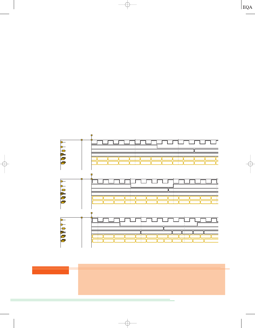
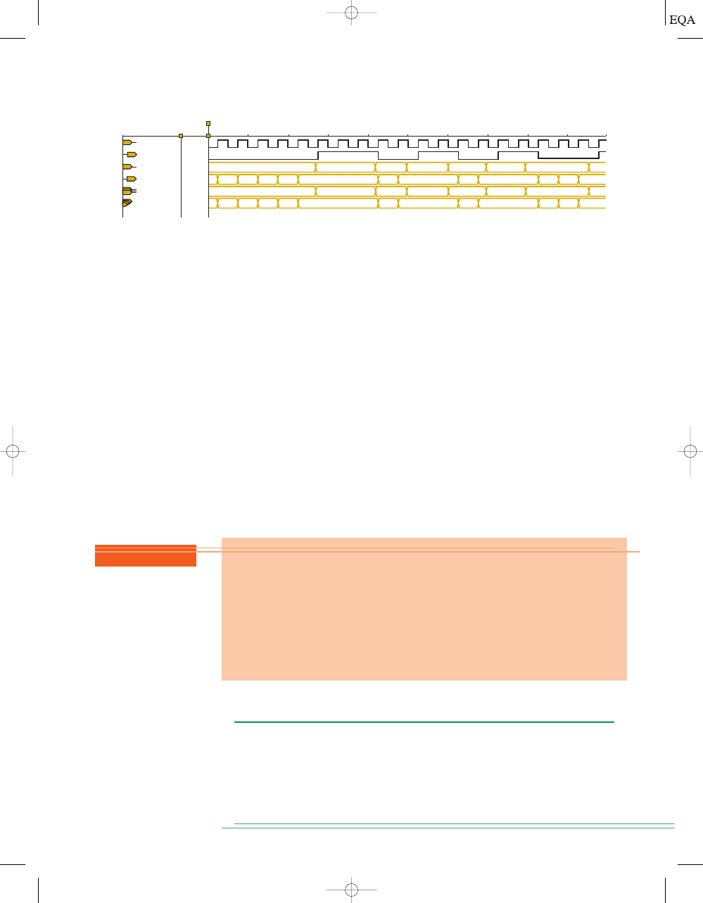
The simulations of Figure 10-10 verify that the circuit seems to be working
properly. Figure 10-10(a) shows each state decoding in mode 0 (full-step) and
completing the cycle in both directions. Notice that after the mode (
m) changes
to
the output (
cout) is decoded as the wave-drive sequence. Figure 10-10(b)
shows the wave-drive (mode 1) sequence in both directions and then changes
the mode to
resulting in the half-step sequence being decoded from the
MOD-8 counter. Finally, Figure 10-10(c) shows the half-step mode cycling up and
starting back down. It then switches to mode 3 (direct-drive) at 7.5 ms, showing
that the data on
cin is transferred asynchronously to the outputs. Notice that the
values chosen for
cin ensure that each bit can go HIGH and LOW.
Final integration and testing should involve more than just simulation. A
real stepper motor and current driver should be connected to the circuit and
tested. In this case, the step rate that the simulation used would probably be
faster than the actual stepper motor could handle and would need to be
slowed down for a real hardware functional test.
10
2
,
01
2
,
686
C
HAPTER
10/
D
IGITAL
S
YSTEM
P
ROJECTS
U
SING
HDL
1001
0110
1010
1001
0101
1001
1010
0100
0001
–
0110
0101
1
3
4
5
6
7
0
6
5
0
7
2
Name:
Value:
1.0 ms
2.0 ms
step
0
dir
1
m[1..0]
B 00
cin[3..0]
B XXXX
00
XXXX
01
(a)
q[2..0]
D 0
cout[3..0]
B 1010
0001
0010
1000
0010
0100
0001
0101
0110
0010
0100
0100
5
7
0
7
6
5
4
6
7
5
6
Name:
Value:
4.0 ms
5.0 ms
step
1
dir
0
m[1..0]
B 11
cin[3..0]
B 0100
01
XXXX
10
(b)
q[2..0]
D 3
cout[3..0]
B 0100
1010
0
6.0 ms
0101
0110
0100
0101
0001
1001
1111
1101
1011
1110
0100
4
6
5
4
3
2
1
7
0
0
5
Name:
Value:
6.0 ms
7.0 ms
step
1
dir
1
m[1..0]
B 10
cin[3..0]
B XXXX
10
XXXX
11
(c)
q[2..0]
D 2
cout[3..0]
B 1001
0111
1
1111
1110
1101
1011
0111
8.0 ms
FIGURE 10-10
Simulation testing of the complete stepper driver.
REVIEW QUESTIONS
1. What are the four modes of operation for this stepper motor driver?
2. What are the inputs for the direct-drive mode?
3. What are the inputs for the wave-drive mode?
4. How many states are in the half-step sequence?
TOCCMC10_0131725793.QXD 12/19/2005 2:13 PM Page 686
10-3
KEYPAD ENCODER PROJECT
Another important skill that we are trying to reinforce is circuit analysis.
That may sound like something out of an analog textbook, but we really
need to be able to analyze and understand how existing digital circuits op-
erate. In this section, we present a circuit and analyze how it operates. Then
we use the skills we have acquired to redesign this circuit and write the code
for it in HDL.
Problem Analysis
To reinforce the encoding concepts of Chapter 9, we present a very useful dig-
ital circuit that encodes a hexadecimal (16-key) keypad into a four-bit binary
output. Encoders such as this generally have a strobe output that indicates
when someone presses and releases a key. Because keypads are often inter-
faced to a microcomputer’s bus system, the encoded outputs should have tri-
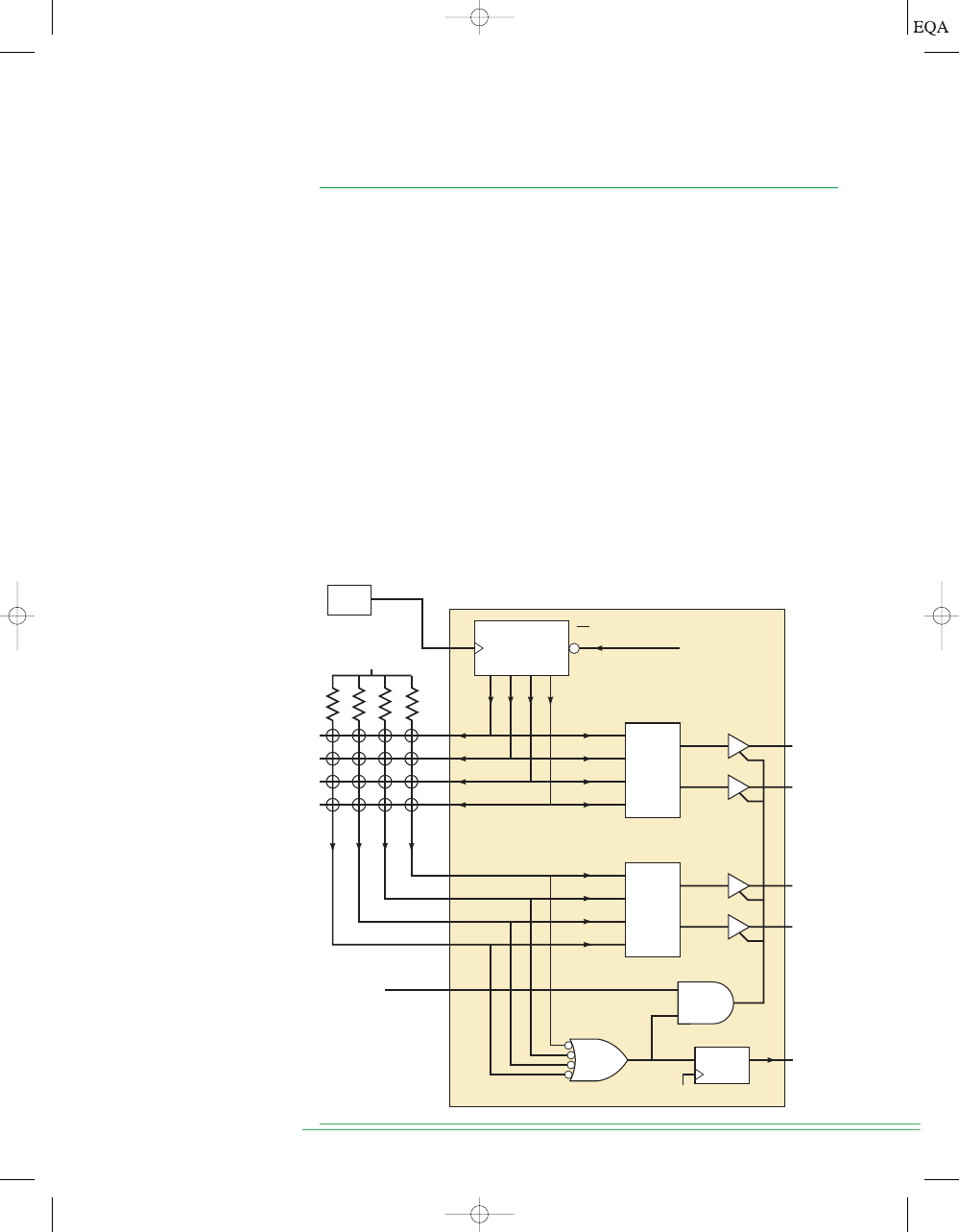
state enables. Figure 10-11 shows the block diagram of the keypad encoder.
The priority encoder method shown in Chapter 9, Figure 9-15, is effective
for small keypads. However, large keyboards such as those found on personal
computers must use a different technique. In these keyboards, each key is
not an independent switch to
or ground. Instead, each key switch is used
V
CC
S
ECTION
10-3/
K
EYPAD
E
NCODER
P
ROJECT
687
D
3
Keypad encoder
D
2
D
1
D
0
Ring
counter
Hexadecimal
keypad
+5 V
CLK
En
Row
Encoder
Freeze
OE
D
Q
CLK
DAV
NAND
Freeze
Column
Encoder
D
3
D
2
D
1
D
0
R
3
R
2
R
1
R
0
C
3
C
2
C
1
C
0
FIGURE 10-11
Keypad
encoder block diagram.
TOCCMC10_0131725793.QXD 12/19/2005 2:13 PM Page 687
to connect a row to a column in the keyboard matrix. When keys are not
pressed, there are no connections between the rows and columns. The trick
of knowing which key is pressed is accomplished by activating (pulling
LOW) one row at a time and then checking to see if any of the columns have
gone LOW. If one of the columns has a LOW on it, then the key being pressed
is at the intersection of the activated row and the column that is currently
LOW. If no columns are LOW, we know that no keys in the activated row are
being pressed and we can check the next row by pulling it LOW. Sequentially
activating rows is called
scanning the keyboard. The advantage of this
method is the reduction in connections to the keypad. In this case, 16 keys
can be encoded using eight inputs/outputs.
Each key represents a unique combination of a row number and a col-
umn number. By strategically numbering the rows and columns, we can com-
bine the binary row and column numbers to create the binary value of the
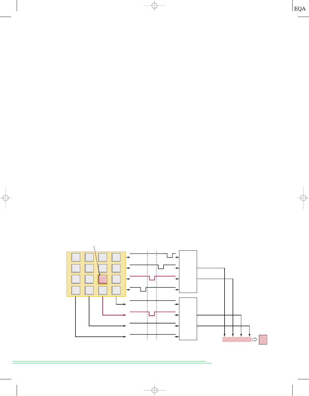
hexadecimal keys as shown in Figure 10-12. In this figure, row 1
is
pulled LOW and the data on the column encoder is
so the button at row
1, column 2 is evidently pressed. The NAND gate in Figure 10-11 is used to
determine if any column is LOW, indicating that a key is pressed in the cur-
rently active row. The output of this gate is named
FREEZE because when a
key is pressed, we want to freeze the ring counter and quit scanning until the
key is released. As the encoders go through their propagation delay and the
tristate buffers become enabled, the data outputs are in a transient state. On
the next rising edge of the clock, the D flip-flop will transfer a HIGH from
FREEZE to the DAV output, indicating that a key is being pressed and the
valid data is available.
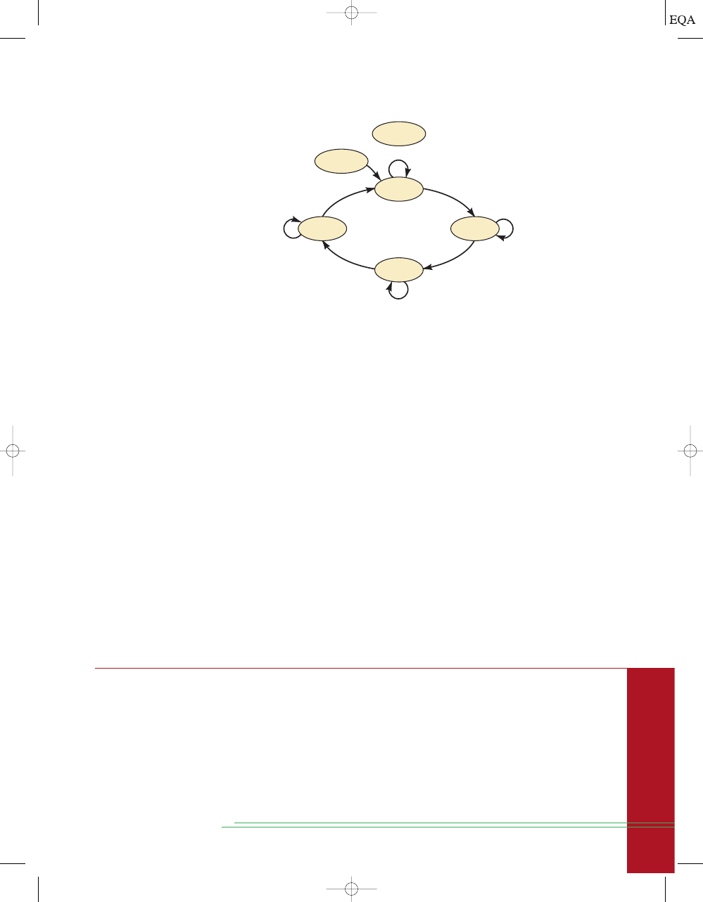
A shift register counter (ring counter), as we studied in Chapter 7, is
used to generate the sequential scan of the four rows. The count sequence
uses four states, each state having a different bit pulled LOW. When a key
press is detected, the ring counter must hold in its current state (freeze) un-
til the key is released. Figure 10-13 shows the state transition diagram. Each
state of this counter must be encoded to generate a two-bit binary row num-
10
2
(01
2
)
688
C
HAPTER
10/
D
IGITAL
S
YSTEM
P
ROJECTS
U
SING
HDL
(11
2
)
(10
2
)
(01
2
)
(00
2
)
D
3
D
2
Row
encoder
F
B
7
3
E
A
2
D
9
5
1
C
8
4
0
Binary
row
number
Row timing
(11
2
)
(10
2
)
(01
2
)
(00
2
)
D
1
D
0
Binary
column
number
Column
encoder
0
1
1
0
6
Column
Row
Key pressed
6
R
3
R
2
R
1
R
0
C
3
C
2
C
1
C
0
FIGURE 10-12
Encoder operation when pressing the “6” key.
TOCCMC10_0131725793.QXD 12/19/2005 2:13 PM Page 688
AHDL
AHDL SOLUTION
The inputs and outputs (see Figure 10-14) are defined on lines 3–8 and follow
the description obtained from analyzing the schematic. The VARIABLE sec-
tion defines several features of this encoder circuit. The freeze bit detects
when a key is pressed. The data node is used to combine the row and column
encoder data. The
ts bit array (line 13) represents a tristate buffer, as we
studied in Chapter 9. Recall that each bit of this buffer has an input,
(
ts[ ].IN), an output (ts.OUT), and an output enable (ts[ ].OE). The data_avail
bit (line 14) represents a D flip-flop with inputs
data_avail.CLK, data_avail.D,
and output
data_avail.Q.
ber. Each column value must also be encoded to generate a two-bit binary
column number. The system will require the following inputs and outputs.
4
Row drive outputs
–
4
Column read inputs
–
4
Encoded data outputs
–
1
Data available strobe output
DAV
1
Tristate enable input
OE
1
Clock input
CLK
Strategic Planning
This circuit is already structured so that we can easily write pieces of HDL
code to emulate each section of the system. The major blocks are as follows:
A ring counter with active-LOW outputs.
Two encoders for the row and column numbers.
Key-press detection and tristate enable circuits.
Because these circuits have been explored in previous chapters, we will not
show the development and testing of each block here. The solutions that fol-
low jump directly to the integration and testing phase of the project.
D
3
D
0
C
3
C
0
R
3
R
0
S
ECTION
10-3/
K
EYPAD
E
NCODER
P
ROJECT
689
R
3
0 1 1 1
1 1 0 1
1 0 1 1
1 1 1 0
FREEZE = 1
FREEZE = 1
FREEZE = 1
FREEZE = 1
FREEZE = 0
FREEZE = 0
FREEZE = 0
FREEZE = 0
R
2
R
1
R
0
All other
states
FIGURE 10-13
Row drive
ring counter state diagram.
TOCCMC10_0131725793.QXD 12/19/2005 2:13 PM Page 689

690
C
HAPTER
10/
D
IGITAL
S
YSTEM
P
ROJECTS
U
SING
HDL
FIGURE 10-14
AHDL scanning keypad encoder.
SUBDESIGN fig10_14
(
clk :INPUT;
col[3..0] :INPUT;
oe :INPUT; --tristate output enable
row[3..0] :OUTPUT;
d[3..0] :OUTPUT;
dav :OUTPUT; --data available
)
VARIABLE
freeze :NODE;
data[3..0] :NODE;
ts[3..0] :TRI;
data_avail :DFF;
ring: MACHINE OF BITS (row[3..0])
WITH STATES (s1 = B”1110”, s2 = B”1101”, s3 = B”1011”, s4 = B”0111”,
% s = ring states %
f1 = B”0001”, f2 = B”0010”, f3 = B”0011”, f4 = B”0100”,
f5 = B”0101”, f6 = B”0110”, f7 = B”1000”, f8 = B”1001”,
f9 = B”1010”, fa = B”1100”, fb = B”1111”, fc = B”0000”);
% f = unused states --> self-correcting design %
BEGIN
ring.CLK = clk;
ring.ENA = !freeze;
data_avail.CLK = clk;
data_avail.D = freeze;
dav = data_avail.Q;
ts[].OE = oe & freeze;
ts[].IN = data[];
d[] = ts[].OUT;
CASE ring IS
WHEN s1 => ring = s2; data[3..2] = B”00”;
WHEN s2 => ring = s3; data[3..2] = B”01”;
WHEN s3 => ring = s4; data[3..2] = B”10”;
WHEN s4 => ring = s1; data[3..2] = B”11”;
WHEN OTHERS => ring = s1;
END CASE;
CASE col[] IS
WHEN B”1110” => data[1..0] = B”00”; freeze = VCC;
WHEN B”1101” => data[1..0] = B”01”; freeze = VCC;
WHEN B”1011” => data[1..0] = B”10”; freeze = VCC;
WHEN B”0111” => data[1..0] = B”11”; freeze = VCC;
WHEN OTHERS => data[1..0] = B”00”; freeze = GND;
END CASE;
END;
1
2
3
4
5
6
7
8
9
10
11
12
13
14
15
16
17
18
19
20
21
22
23
24
25
26
27
28
29
30
31
32
33
34
35
36
37
38
39
40
41
42
43
44
45
46
47
TOCCMC10_0131725793.QXD 12/19/2005 2:13 PM Page 690
VHDL
Lines 15–20 demonstrate a powerful feature of AHDL that allows us to
define a state machine, with each state made up of the bit pattern we
need. On line 15, the name
ring was given to this state machine because it
acts like a ring counter. The bits that make up this ring counter machine
are the four row bits that were defined on line 6. These states are labeled
s1–s4 and have their bit patterns assigned to them so that one bit of the
four is LOW for each state, like an active-LOW ring counter. The other
twelve states are specified by an arbitrary label that starts with
f to indi-
cate they are not valid states. Lines 23 through 30 essentially connect all
the components as shown in the circuit drawing of Figure 10-11. Both the
ring count sequence and the encoding of the row value are described on
lines 32–38. For each PRESENT state value of
ring, the NEXT state is de-
fined as well as the proper output of the row encoder (
data[3..2]). Line 37
ensures that this counter will self-start by sending it to
s1 from any state
other than
s1–s4. The encoding of the column value is described on lines
40–46. Notice that the generation of the
freeze signal in this design does
not follow the diagram of Figure 10-11 exactly. In this design, rather than
NANDing the columns, the CASE structure activates
freeze only when one
(and only one) column is LOW. Thus, if multiple keys in the same row were
pressed, the encoder would not recognize any as a valid key press and
would not activate
dav.
S
ECTION
10-3/
K
EYPAD
E
NCODER
P
ROJECT
691
VHDL SOLUTION
Compare the VHDL description in Figure 10-15 with the circuit drawing of
Figure 10-11. The inputs and outputs are defined on lines 5–9 and follow the
description obtained from analyzing the schematic. Two SIGNALs are de-
fined on lines 13 and 14 for this design. The
freeze bit detects when a key is
pressed. The
data signal is used to combine the row and column encoder data
to make a four-bit value representing the key that was pressed. The ring
counter is implemented using a PROCESS that responds to the
clk input.
Line 26 ensures that this counter will self-start by sending it to state “1110”
from any state other than those in the
ring sequence. Notice that on line 20,
the status of
freeze is checked before a CASE is used to assign a NEXT state
to
ring. This is the way the count enable is implemented in this design. On
line 29, the data available output (
dav) is updated synchronously with the
value of
freeze. It is synchronous because it is within the IF structure (lines
19–30) that detects the active clock edge. The remaining statements (lines
31–52) do not depend on the active clock edge but describe what the circuit
will do on either edge of the clock.
The encoding of the row value is described on lines 33–39. For each
PRESENT state value of
ring, the output of the row encoder data(3
DOWNTO 2) is defined. The encoding of the column value is described on
lines 41–47. Notice that the generation of the
freeze signal in this design does
not follow the diagram of Figure 10-11 exactly. In this design, rather than
NANDing the columns, the CASE structure activates
freeze only when one
(and only one) column is LOW. Thus, if multiple keys in the same row were
pressed, the encoder would not recognize any as a valid key press and would
not activate
dav.
TOCCMC10_0131725793.QXD 12/19/2005 2:13 PM Page 691

692
C
HAPTER
10/
D
IGITAL
S
YSTEM
P
ROJECTS
U
SING
HDL
LIBRARY ieee;
USE ieee.std_logic_1164.all;
ENTITY fig10_15 IS
PORT ( clk :IN STD_LOGIC;
col :IN STD_LOGIC_VECTOR (3 DOWNTO 0);
row :OUT STD_LOGIC_VECTOR (3 DOWNTO 0);
d :OUT STD_LOGIC_VECTOR (3 DOWNTO 0);
dav :OUT STD_LOGIC );
END fig10_15;
ARCHITECTURE vhdl OF fig10_15 IS
SIGNAL freeze :STD_LOGIC;
SIGNAL data :STD_LOGIC_VECTOR (3 DOWNTO 0);
BEGIN
PROCESS (clk)
VARIABLE ring :STD_LOGIC_VECTOR (3 DOWNTO 0);
BEGIN
IF (clk’EVENT AND clk = ’1’) THEN
IF freeze = ’0’ THEN
CASE ring IS
WHEN “1110” => ring := “1101”;
WHEN “1101” => ring := “1011”;
WHEN “1011” => ring := “0111”;
WHEN “0111” => ring := “1110”;
WHEN OTHERS => ring := “1110”;
END CASE;
END IF;
dav <= freeze;
END IF;
row <= ring;
CASE ring IS
WHEN “1110” => data(3 DOWNTO 2) <= “00”;
WHEN “1101” => data(3 DOWNTO 2) <= “01”;
WHEN “1011” => data(3 DOWNTO 2) <= “10”;
WHEN “0111” => data(3 DOWNTO 2) <= “11”;
WHEN OTHERS => data(3 DOWNTO 2) <= “00”;
END CASE;
CASE col IS
WHEN “1110” => data(1 DOWNTO 0) <= “00”; freeze <= ’1’;
WHEN “1101” => data(1 DOWNTO 0) <= “01”; freeze <= ’1’;
WHEN “1011” => data(1 DOWNTO 0) <= “10”; freeze <= ’1’;
WHEN “0111” => data(1 DOWNTO 0) <= “11”; freeze <= ’1’;
WHEN OTHERS => data(1 DOWNTO 0) <= “00”; freeze <= ’0’;
END CASE;
IF freeze = ’1’ THEN d <= data;
ELSE d <= “ZZZZ”;
END IF;
END PROCESS;
END vhdl;
FIGURE 10-15
VHDL scanning
keypad encoder.
1
2
3
4
5
6
7
8
9
10
11
12
13
14
15
16
17
18
19
20
21
22
23
24
25
26
27
28
29
30
31
32
33
34
35
36
37
38
39
40
41
42
43
44
45
46
47
48
49
50
51
52
53
TOCCMC10_0131725793.QXD 12/19/2005 2:13 PM Page 692
The simulation of the project is shown in Figure 10-16. The column val-
ues (
col) are entered by the designer as a test input that simulates the value
being read from the columns of the keypad as the rows are being scanned. As
long as all columns are HIGH (i.e., the hex value F is on
col), the ring counter
is enabled and counting,
dav is LOW, and the d outputs are in the Hi-Z state.
Just before the 3.0-ms mark, a 7 is simulated as a
col input, which means that
one of the columns went LOW. This simulates a key being detected in the
most significant column (C3) of the keypad matrix. Notice that as a result of
the column going LOW, on the next active (rising) clock edge, the
dav line
goes HIGH and the ring counter does not change state. It is disabled from go-
ing to its NEXT state as long as the key is pressed. At this point, the
row
value is E hex (
), which means that the least significant row (R0) is be-
ing pulled LOW by the ring counter. The row encoder translates this into the
binary row number (00). The key located at the intersection of the least sig-
nificant row
and the most significant column
is the 3 key (see
Figure 10-12). At this point, the
d outputs hold the encoded key value of 3
. Just after the 4-ms mark, the simulation imitates the release of the
key by changing the column value back to F hex, which causes the
d output
to go into its Hi-Z state. On the next rising clock edge, the
dav line goes LOW
and the ring counter resumes its count sequence.
(0011
2
)
(11
2
)
(00
2
)
1110
2
S
ECTION
10-4/
D
IGITAL
C
LOCK
P
ROJECT
693
Name:
Value:
1.0 ms
2.0 ms
3.0 ms
4.0 ms
5.0 ms
6.0 ms
7.0 ms
8.0 ms
9.0 ms
10 ms
clk
0
dav
0
col
H F
row
H 0
d
H Z
ring
H D
0
E
B
7
E
D
B
7
E
D
B
7
F
7
F
E
F
D
F
B
0
D
B
7
E
D
B
7
E
D
B
7
E
Z
3
Z
8
Z
1
Z
E
D
FIGURE 10-16
Simulation of the scanning keypad encoder.
REVIEW QUESTIONS
1. How many rows on the scanned keyboard are activated at any point in
time?
2. If two keys in the same column are pressed simultaneously, which key
will be encoded?
3. What is the purpose of the D flip-flop on the DAV pin?
4. Will the time between the key being pressed and DAV going HIGH
always be the same?
5. When are the data output pins in the Hi-Z state?
10-4
DIGITAL CLOCK PROJECT
One of the most common applications of counters is the digital clock—a time
clock that displays the time of day in hours, minutes, and sometimes seconds.
In order to construct an accurate digital clock, a closely controlled basic
clock frequency is required. For battery-operated digital clocks or watches,
the basic frequency is normally obtained from a quartz-crystal oscillator.
Digital clocks operated from the ac power line can use the
60-Hz power fre-
quency as the basic clock frequency. In either case, the basic frequency must
TOCCMC10_0131725793.QXD 12/19/2005 2:13 PM Page 693
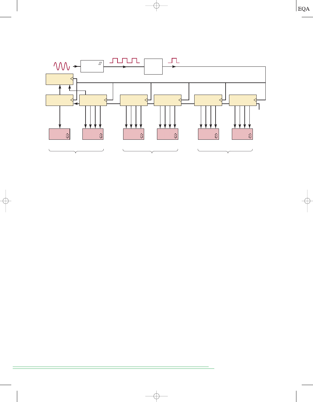
be divided to a frequency of 1 Hz or 1 pulse per second (pps). Figure 10-17
shows the basic block diagram for a digital clock operating from 60 Hz.
The
60-Hz signal is sent through a Schmitt-trigger circuit to produce
square pulses at the rate of 60 pps. This 60-pps waveform is fed into a MOD-
60 counter that is used to divide the 60 pps down to 1 pps. The 1-pps signal is
used as a synchronous clock for all of the counter stages, which are synchro-
nously cascaded. The first stage is the SECONDS section, which is used to
count and display seconds from 0 through 9. The
BCD counter advances one
count per second. When this stage reaches 9 seconds, the BCD counter acti-
vates its terminal count output (
tc), and on the next active clock edge, it re-
cycles to 0. The BCD terminal count enables the MOD-6 counter and causes
it to advance by one count at the same time that the BCD counter recycles.
This process continues for 59 seconds, at which point the MOD-6 counter is
at the 101 (5) count and the BCD counter is at 1001 (9) so that the display
reads 59 s and
tc of the MOD-6 is HIGH. The next pulse recycles the BCD
counter and the MOD-6 counter to zero (remember, the MOD-6 counts from
0 through 5).
The
tc output of the MOD-6 counter in the SECONDS section has a fre-
quency of 1 pulse per minute (i.e, the MOD-6 recycles every 60 s). This signal
is fed to the MINUTES section, which counts and displays minutes from 0
through 59. The MINUTES section is identical to the SECONDS section and
operates in exactly the same manner.
The
tc output of the MOD-6 counter in the MINUTES section has a fre-
quency of 1 pulse per hour (i.e., the MOD-6 recycles every 60 min). This sig-
nal is fed to the HOURS section, which counts and displays hours from 1
through 12. This HOURS section is different from the SECONDS and MIN-
UTES sections because it never goes to the 0 state. The circuitry in this sec-
tion is sufficiently unusual to warrant a closer investigation.
Figure 10-18 shows the detailed circuitry contained in the HOURS sec-
tion. It includes a BCD counter to count units of hours and a single FF (MOD-
2) to count tens of hours. The BCD counter is a 74160, which has two active-
HIGH inputs, ENT and ENP, that are ANDed together internally to enable the
694
C
HAPTER
10/
D
IGITAL
S
YSTEM
P
ROJECTS
U
SING
HDL
Decoder/
display
Decoder/
display
0-5
Tens
0-9
Units
''Seconds'' section
Decoder/
display
Decoder/
display
0-5
Tens
0-9
Units
''Minutes'' section
Decoder/
display
0-9
Units
''Hours'' section
60 Hz
Pulse
shaper
60 pps
CTR
DIV60
1 pps
MOD-2
(one FF)
0-1
Tens
AM/PM
(one FF)
En
TC
En
TC
En
TC
En
TC
En
1 pps
Display
1 pulse/hr
1 pulse/min
V
CC
BCD
counter
BCD
counter
BCD
counter
MOD-6
counter
MOD-6
counter
FIGURE 10-17
Block diagram for a digital clock.
TOCCMC10_0131725793.QXD 12/19/2005 2:13 PM Page 694

count. The ENT input also enables the active-HIGH ripple carry out (RCO)
that detects the BCD terminal count of 9. The ENT input and RCO output can
therefore be used for synchronous counter cascading. The ENP input is tied
HIGH so that the counter will increment whenever ENT is HIGH.
The hours counter is enabled by the minutes and seconds stages for only
one clock pulse every hour. When this condition occurs, ENT is HIGH, which
means that the minutes:seconds stages are at 59:59. For example, at 9:59:59, the
tens of hours flip-flop holds a 0, the 74160 holds
(9), and the RCO output
is HIGH, putting the tens of hours flip-flop in the SET mode. The two display
digits for the hours show 09. On the next rising clock edge, the BCD counter ad-
vances to its natural NEXT state of
, RCO goes LOW, and the tens of hours
flip-flop advances to 1 so that the hours display digits now show 10.
When it is 11:59:59, AND gate 1 detects that the tens of hours is 1 and the
enable input is active (previous stages are at 59:59). AND gate 3 combines
the conditions of AND gate 1 and the condition that the BCD counter is in the
state
The output of AND gate 3 will be HIGH only at 11:59:59 in the
hours count sequence. On the next clock pulse, the AM/PM flip-flop toggles,
indicating noon (HIGH) or midnight (LOW). At the same time, the BCD
counter advances to 2 and the minutes:seconds stages roll over to 00:00, re-
sulting in a BCD display of 12:00:00. At 12:59:59, AND gate 1 detects that the
tens digit is 1 and it is time to advance the hours. AND gate 2 detects that the
BCD counter is at 2. The output of AND gate 2 prepares to do two tasks on
the next clock edge: reset the tens of hours flip-flop, and load the 74160
counter with the value
After the next clock pulse, it is 01:00:00 o’clock.
The operation of counter circuits should make sense now, and you should
have a good grasp on how you can connect MSI chips to make this digital clock.
0001
2
.
0001
2
.
0000
2
1001
2
S
ECTION
10-4/
D
IGITAL
C
LOCK
P
ROJECT
695
QA
QB
QC
QD
Counter
74160
RCO
LDN
A
B
C
D
ENT
CLRN
ENP
CLK
units_hrs[0]
VCC
GND
clock
en_hrs
units_hrs[1]
units_hrs[2]
units_hrs[3]
Q
J
K
PRN
CLRN
AM/PM
Q
J
K
PRN
CLRN
Tens of Hours
Units of Hours
PM
tens_hrs
3
1
2
tens_hrs
en_hrs
FIGURE 10-18
Detailed circuitry for the HOURS section.
TOCCMC10_0131725793.QXD 12/19/2005 2:13 PM Page 695
Notice that it is really made up of several small and relatively simple circuits
that are strategically interconnected to make the clock. Recall that in Chapter
4, we mentioned briefly the concept of modular, hierarchical design and de-
velopment of digital systems. Now it is time to apply these principles to a proj-
ect that is within your scope of understanding using the
or
Quartus II development system from Altera. You must understand the opera-
tion of the circuits that have just been described before proceeding with the
design of this clock using HDL. Take some time to review this material.
Top-Down Hierarchical Design
Top-down design means that we want to start at the highest level of com-
plexity in the hierarchy, or that the entire project is considered to exist in a
closed, dark box with inputs and outputs. The details regarding what is in the
box are not yet known. We can only say at this point how we want it to be-
have. The digital clock was chosen because everyone is familiar with the end
result of the operation of this device. An important aspect of this stage of the
design process is establishing the scope of the project. For example, this dig-
ital clock is not going to have a way to set the time, set an alarm time, shut
off the alarm, snooze, or incorporate other features that you may find on the
clock beside your bed. To add all these features now would only clutter the ex-
ample with unnecessary complexity for our immediate purpose. We are also
not going to include the signal conditioning that transforms a 60-Hz sine
wave into a 60-pulse-per-second digital waveform, or the decoder/display cir-
cuits. The project we are tackling has the following specifications:
Inputs:
60 pps CMOS compatible waveform (accuracy dependent on
line frequency)
Outputs: BCD Hours:
1 bit TENS
4 bits UNITS
BCD Minutes: 3 bits TENS 4 bits UNITS
BCD Seconds: 3 bits TENS 4 bits UNITS
PM indicator
Minutes and Seconds sequence: BCD MOD 60
00–59 (decimal representation of BCD)
Hours sequence BCD MOD 12
01–12 (decimal representation of BCD)
Overall range of display
01:00:00–12:59:59
AM/PM indicator toggles at 12:00:00
A
hierarchy is a group of objects arranged in rank order of magnitude,
importance, or complexity. A block diagram of the overall project (highest
level of the hierarchy) is shown in Figure 10-19. Notice that there are four
bits for each of the BCD units outputs and only three bits for each of the
MAX + PLUS
II
696
C
HAPTER
10/
D
IGITAL
S
YSTEM
P
ROJECTS
U
SING
HDL
SEC_ONES[3 . . 0]
SEC_TENS[2 . . 0]
MIN_ONES[3 . . 0]
MIN_TENS[2 . . 0]
HR_ONES[3 . . 0]
HR_TENS
PM
clock
60_PPS
FIGURE 10-19
The top level
block of the hierarchy.
TOCCMC10_0131725793.QXD 12/19/2005 2:13 PM Page 696

minute and second BCD tens outputs. Because the most significant BCD
digit for the tens place is 5
only three bits are needed. Notice also
that the tens place for the hours (HR_TENS) is only one bit. It will never
have a value other than 0 or 1.
The next phase is to break this problem into more manageable sections.
First, we need to take the 60-pps input and transform it into a 1-pulse-per-
second timing signal. A circuit that divides a reference frequency to a rate
required by the system is called a
prescaler. Next, it makes sense to have in-
dividual sections for a seconds counter, minutes counter, and hours counter.
So far, the hierarchy diagram looks like Figure 10-20, which shows the proj-
ect broken into four subsections.
The entire purpose of the frequency prescaler section is to divide the 60-
pps input to a frequency of one pulse every second. This requires a MOD-60
counter, and the sequence of the count does not really matter. In this example,
the minutes and seconds sections both require MOD-60 counters that count
from 00–59 in BCD. Looking for similarities like this is very important in the de-
sign process. In this case, we can use the exact same circuit design to imple-
ment the frequency prescaler, the minutes counter, and the seconds counters.
A MOD-60 BCD counter can be made quite easily from a MOD-10
(decade) counter cascaded to a MOD-6 BCD counter, as we saw in the dia-
gram of Figure 10-17. This means that inside each of these MOD-60 blocks,
we would find a diagram similar to Figure 10-21. The hierarchy of the project
now appears as shown in Figure 10-22.
(101
2
),
S
ECTION
10-4/
D
IGITAL
C
LOCK
P
ROJECT
697
Digital clock
Hours
Minutes
Seconds
Frequency
prescaling
FIGURE 10-20
The
section level of the
hierarchy.
Q[3 . . 0]
CLKMOD10
TC
CLK
ENA
Q[2 . . 0]
CLKMOD6
TC
CLK
ENA
enable
ones[3..0]
tens[2..0]
TC
clk
FIGURE 10-21
The blocks inside the MOD-60 section.
Digital clock
Hours MOD 12
Minutes
Seconds
Frequency
prescaling
MOD-6
MOD-10
MOD-6
MOD-10
MOD-6
MOD-10
FIGURE 10-22
The complete hierarchy of the clock project.
TOCCMC10_0131725793.QXD 12/19/2005 2:13 PM Page 697
The final design decision is whether or not to break down the MOD-12
section for Hours into two stages, as shown in Figure 10-18. One option is to
connect the macrofunctions of these standard parts from the HDL library, as
we have discussed in previous chapters. Because this circuit is rather un-
usual, we have decided instead to describe the MOD-12 hours counter using
a single HDL module. We will also describe the MOD-6 and MOD-10 building
blocks using HDL. The entire clock circuit can then be built using these
three basic circuit descriptions. Of course, even these blocks can be broken
down into smaller flip-flop blocks and designed using the schematic entry,
but it will be much easier using HDL at this level.
Building the Blocks from the Bottom Up
Each of the basic blocks are presented here in both AHDL and VHDL. We
present the MOD-6 as a simple modification of the MOD-5 synchronous
counter descriptions presented earlier in Chapter 7 (see Figures 7-39 and
7-40). Then we modify this code further to create the MOD-10 counter and
finally design the MOD-12 Hours counter from the ground up. We construct
the entire clock from these three basic blocks.
698
C
HAPTER
10/
D
IGITAL
S
YSTEM
P
ROJECTS
U
SING
HDL
FIGURE 10-23
The MOD-6 design in AHDL.
SUBDESIGN fig10_23
(
clock, enable :INPUT; -- synch clock and enable.
q[2..0], tc :OUTPUT; -- 3-bit counter
)
VARIABLE
count[2..0] :DFF; -- declare a register of D flip-flops.
BEGIN
count[].clk = clock; -- connect all clocks to synchronous source
IF enable THEN
IF count[].q < 5 THEN
count[].d = count[].q + 1; -- increment current value by one
ELSE count[].d = 0; -- recycle,force unused states to 0
END IF;
ELSE count[].d = count[].q; -- not enabled: hold at this count
END IF;
tc = enable & count[].q == 5; -- detect maximum count if enabled
q[] = count[].q; -- connect register to outputs
END;
1
2
3
4
5
6
7
8
9
10
11
12
13
14
15
16
17
18
19
20
MOD-6 COUNTER AHDL
The only additional features that this design needs that are not covered in
Figure 7-39 are the count
enable input and terminal count (tc) output shown
in Figure 10-23. Notice that the extra input (
enable, line 3) and output (tc,
line 4) are included in the I/O definition. A new line (line 11) in the archi-
tecture description tests
enable before deciding how to update the value of
AHDL
TOCCMC10_0131725793.QXD 12/19/2005 2:13 PM Page 698
count (lines 12–15). If enable is LOW, the same value is held on count at every
clock edge by the ELSE branch (line 16). Remember always to match an IF
with an END IF, as we did on lines 15 and 17. Terminal count (
tc, line 18) will
be HIGH when it is
true that AND
enable is active. Notice the use
of double equal signs
to evaluate equality in AHDL.
( =
=
)
count
=
=
5
S
ECTION
10-4/
D
IGITAL
C
LOCK
P
ROJECT
699
FIGURE 10-24
The MOD-6 design in VHDL.
ENTITY fig10_24 IS
PORT( clock, enable :IN BIT ;
q :OUT INTEGER RANGE 0 TO 5;
tc :OUT BIT
);
END fig10_24;
ARCHITECTURE a OF fig10_24 IS
BEGIN
PROCESS (clock) -- respond to clock
VARIABLE count :INTEGER RANGE 0 TO 5;
BEGIN
IF (clock = ’1’ AND clock’event) THEN
IF enable = ’1’ THEN -- synchronous cascade input
IF count < 5 THEN -- < max (terminal) count?
count := count + 1;
ELSE
count := 0;
END IF;
END IF;
END IF;
IF (count = 5) AND (enable = ’1’) THEN -- synch cascade output
tc <= ’1’; -- indicate terminal ct
ELSE tc <= ’0’;
END IF;
q <= count; -- update outputs
END PROCESS;
END a;
1
2
3
4
5
6
7
8
9
10
11
12
13
14
15
16
17
18
19
20
21
22
23
24
25
26
27
28
29
MOD-6 COUNTER VHDL
The only additional features that this design needs that are not covered in
Figure 7-40 are the count
enable input and terminal count (tc) output
shown in Figure 10-24. Notice that the extra input (
enable, line 2) and out-
put (
tc, line 4) are included in the I/O definition. A new line (line 15) in the
architecture description tests
enable before deciding how to update the
value of
count (lines 16–20). In the case that enable is LOW, the current
value is held in the variable
count and does not count up. Remember al-
ways to match an IF with an END IF, as we did on lines 20–22. The termi-
nal count indicator (
tc, lines 23 and 24) will be HIGH when it is true that
AND
enable is active.
count = 5
VHDL
TOCCMC10_0131725793.QXD 12/19/2005 2:13 PM Page 699
The simulation testing of the MOD-6 counter in Figure 10-25 verifies that
it counts 0–5 and that it responds to the count enable input by ignoring the
clock pulses and freezing the count whenever
enable is LOW. It also gener-
ates the
tc output when it is enabled at its maximum count of 5.
700
C
HAPTER
10/
D
IGITAL
S
YSTEM
P
ROJECTS
U
SING
HDL
1
2
3
4
5
0
1
2
3
4
5
0
1
0
2
1
2
3
4
5
0
1
2
3
4
5
0
1
0
2
Name:
Value:
1.0 ms
2.0 ms
3.0 ms
4.0 ms
5.0 ms
6.0 ms
7.0 ms
8.0 ms
9.0 ms
10 ms
enable
0
clock
0
tc
0
q[2 . . 0]
H0
count[2. . .0]
H0
FIGURE 10-25
Simulation of the MOD-6 counter.
AHDL
FIGURE 10-26
The MOD-10 design in AHDL.
SUBDESIGN fig10_26
(
clock, enable :INPUT; -- synch clock and enable.
q[3..0], tc :OUTPUT; -- 4-bit Decade counter
)
VARIABLE
count[3..0] :DFF; -- declare a register of D flip flops.
BEGIN
count[].clk = clock; -- connect all clocks to synchronous source
IF enable THEN
IF count[].q < 9 THEN
count[].d = count[].q + 1; -- increment current value by one
ELSE count[].d = 0; -- recycle,force unused states to 0
END IF;
ELSE count[].d = count[].q; -- not enabled: hold at this count
END IF;
tc = enable & count[].q == 9; -- detect maximum count
q[] = count[].q; -- connect register to outputs
END;
1
2
3
4
5
6
7
8
9
10
11
12
13
14
15
16
17
18
19
20
VHDL
MOD-10 COUNTER VHDL
The MOD-10 counter varies only slightly from the MOD-6 counter that was
described in Figure 10-24. The only changes that are necessary involve
changing the number of bits in the output port and the variable
count (using
INTEGER RANGE) along with the maximum value that the counter should
reach before rolling over. Figure 10-27 presents the MOD-10 design.
MOD-10 COUNTER AHDL
The MOD-10 counter varies only slightly from the MOD-6 counter that was
described in Figure 10-23. The only changes that are necessary involve
changing the number of bits in the output port and the register (in the
VARIABLE section) along with the maximum value that the counter should
reach before rolling over. Figure 10-26 presents the MOD-10 design.
TOCCMC10_0131725793.QXD 12/19/2005 2:13 PM Page 700
MOD 12 Design
We have already decided that the hours counter is to be implemented as a
single design file using HDL. It must be a MOD-12 BCD counter that follows
the hours sequence of a clock (1–12) and provides the AM/PM indicator.
Recall from the initial design step that the BCD outputs need to be a four-bit
array for the low-order digit and a single bit for the high-order digit. To de-
sign this counter circuit, consider how it needs to operate. Its sequence is:
By observing this sequence, we can conclude that there are four critical ar-
eas that define the operations needed to produce the proper NEXT state:
1. When the value is 01 through 08, increment the low digit and keep the
high digit the same.
2. When the value is 09, reset the low digit to 0 and force the high digit to 1.
3. When the value is 10 or 11, increment the low digit and keep the high
digit the same.
4. When the value is 12, reset the low digit to 1 and the high digit to 0.
Because these conditions need to evaluate a range of values, it is most ap-
propriate to use an IF/ELSIF construct rather than a CASE construct. There
01
02
03
04
05
06
07
08
09
10
11
12
01 Á
S
ECTION
10-4/
D
IGITAL
C
LOCK
P
ROJECT
701
FIGURE 10-27
The MOD-10 design in VHDL.
ENTITY fig10_27 IS
PORT( clock, enable :IN BIT ;
q :OUT INTEGER RANGE 0 TO 9;
tc :OUT BIT
);
END fig10_27;
ARCHITECTURE a OF fig10_27 IS
BEGIN
PROCESS (clock) -- respond to clock
VARIABLE count :INTEGER RANGE 0 TO 9;
BEGIN
IF (clock = ’1’ AND clock’event) THEN
IF enable = ’1’ THEN -- synchronous cascade input
IF count < 9 THEN -- decade counter
count := count + 1;
ELSE
count := 0;
END IF;
END IF;
END IF;
IF (count = 9) AND (enable = ’1’) THEN -- synch cascade output
tc <= ’1’;
ELSE tc <= ’0’;
END IF;
q <= count; -- update outputs
END PROCESS;
END a;
1
2
3
4
5
6
7
8
9
10
11
12
13
14
15
16
17
18
19
20
21
22
23
24
25
26
27
28
29
TOCCMC10_0131725793.QXD 12/19/2005 2:13 PM Page 701
is also a need to identify when it is time to toggle the AM/PM indicator. This
time occurs when the hour state is 11 and the enable is HIGH, which means
that the lower-order counters are at their maximum (59:59).
702
C
HAPTER
10/
D
IGITAL
S
YSTEM
P
ROJECTS
U
SING
HDL
AHDL
FIGURE 10-28
The MOD-12 hours counter in AHDL.
SUBDESIGN fig10_28
(
clk, ena :INPUT;
low[3..0], hi, pm :OUTPUT;
)
VARIABLE
low[3..0] :DFF;
hi :DFF;
am_pm :JKFF;
time :NODE;
BEGIN
low[].clk = clk; -- synchronous clocking
hi.clk = clk;
am_pm.clk = clk;
IF ena THEN -- use enable to count
IF low[].q < 9 & hi.q == 0 THEN
low[].d = low[].q + 1; --inc lo digit
hi.d = hi.q; -- hold hi digit
ELSIF low[].q == 9 THEN
low[].d = 0;
hi.d = VCC;
ELSIF hi.q == 1 & low[].q < 2 THEN
low[].d = low[].q + 1;
hi.d = hi.q;
ELSIF hi.q == 1 & low[].q == 2 THEN
low[].d = 1;
hi.d = GND;
END IF;
ELSE
low[].d = low[].q;
hi.d = hi.q;
END IF;
time = hi.q == 1 & low[3..0].q == 1 & ena; -- detect 11:59:59
am_pm.j = time; -- toggle am/pm at noon and midnight
am_pm.k = time;
pm = am_pm.q;
END;
1
2
3
4
5
6
7
8
9
10
11
12
13
14
15
16
17
18
19
20
21
22
23
24
25
26
27
28
29
30
31
32
33
34
35
36
37
MOD-12 COUNTER IN AHDL
The AHDL counter needs a bank of four D flip-flops for the low-order BCD
digit and only a single D flip-flop for the high-order BCD digit because its
value will always be 0 or 1. A flip-flop is also needed to keep track of
A
.
M
. and
P
.
M
. These primitives are declared on lines 7–9 of Figure 10-28. Also note that
in this design, the same names are used for the output ports. This is a con-
venient feature of AHDL. When the enable input (
ena) is active, the circuit
evaluates the IF/ELSE statements of lines 16–28 and performs the proper
TOCCMC10_0131725793.QXD 12/19/2005 2:13 PM Page 702
operation on the high and low nibble of the BCD number. Whenever the en-
able input is LOW, the value remains the same, as shown on lines 30 and 31.
Line 33 detects when the count reaches 11 while the counter is enabled. This
signal is applied to the
J and K inputs of the am_pm flip-flop to cause it to
toggle at 11:59:59.
S
ECTION
10-4/
D
IGITAL
C
LOCK
P
ROJECT
703
FIGURE 10-29
The MOD-12 hours counter in VHDL.
VHDL
ENTITY fig10_29 IS
PORT( clk, ena :IN BIT ;
low :OUT INTEGER RANGE 0 TO 9;
hi :OUT INTEGER RANGE 0 TO 1;
pm :OUT BIT );
END fig10_29;
ARCHITECTURE a OF fig10_29 IS
BEGIN
PROCESS (clk) -- respond to clock
VARIABLE am_pm :BIT;
VARIABLE ones :INTEGER RANGE 0 TO 9; -- 4-bit units signal
VARIABLE tens :INTEGER RANGE 0 TO 1; -- 1-bit tens signal
BEGIN
IF (clk = '1' AND clk'EVENT) THEN
IF ena = '1' THEN -- synchronous cascade input
IF (ones = 1) AND (tens = 1) THEN -- at 11:59:59
am_pm := NOT am_pm; -- toggle am/pm
END IF;
IF (ones < 9) AND (tens = 0) THEN -- states 00-08
ones := ones + 1; -- increment units
ELSIF ones = 9 THEN -- state 09...set to 10:00
ones := 0; -- units reset to zero
tens := 1; -- tens bump up to 1
ELSIF (tens = 1) AND (ones < 2) THEN-- states 10, 11
ones := ones + 1; -- increment units
ELSIF (tens = 1) AND (ones = 2) THEN -- state 12
ones := 1; -- set to 01:00
tens := 0;
END IF;
-----------------------------------------------------------
-- This space is the alternate location for updating am/pm
-----------------------------------------------------------
END IF;
END IF;
pm <= am_pm;
low <= ones; -- update outputs
hi <= tens;
END PROCESS;
END a;
1
2
3
4
5
6
7
8
9
10
11
12
13
14
15
16
17
18
19
20
21
22
23
24
25
26
27
28
29
30
31
32
33
34
35
36
37
38
39
40
MOD-12 COUNTER IN VHDL
The VHDL counter of Figure 10-29 needs a four-bit output for the low-order
BCD digit and a single output bit for the high-order BCD digit because its
TOCCMC10_0131725793.QXD 12/19/2005 2:13 PM Page 703
value will always be 0 or 1. These outputs (lines 3 and 4) and also the vari-
ables that will produce the outputs (lines 12 and 13) are declared as integers
because this makes “counting” possible by simply adding 1 to the variable
value. On each active edge of the clock, when the enable input is active, the
circuit needs to decide what to do with the BCD units-of-hours counter, the sin-
gle bit tens-of-hours flip-flop, and also the AM/PM flip-flop.
This example is an excellent opportunity to point out some of the ad-
vanced features of VHDL that allow the designer to describe precisely the
operation of the final hardware circuit. In previous chapters, we discussed
the issue of statements within a PROCESS being evaluated sequentially.
Recall that statements outside the PROCESS are considered concurrent,
and the order in which they are written in the design file has no effect on the
operation of the final circuit. In this example, we must evaluate the current
state to decide whether to toggle the AM/PM indicator and also advance the
counter to the NEXT state. The issues involved include the following:
1. How do we “remember” the current count value in VHDL?
2. Do we evaluate the current count to see if it is 11 (to determine if we
need to toggle the AM/PM flip-flop) and then increment to 12, or do we
increment the counter’s state from 11 to 12 and then evaluate the count
to see if it is 12 (to know we need to toggle the AM/PM flip flop)?
Regarding the first issue, there are two ways to remember the current
state of a counter in VHDL. Both SIGNALs and VARIABLEs hold their value
until they are updated. Generally, SIGNALs are used to connect nodes in
the circuit like wires, and VARIABLEs are used like a register to store data
between updates. Consequently, VARIABLEs are generally used to imple-
ment counters. The major differences are that VARIABLEs are local to the
PROCESS in which they are declared and SIGNALs are global. Also,
VARIABLEs are considered to be updated immediately within a sequence of
statements in a PROCESS, whereas SIGNALs referred to in a PROCESS are
updated when the PROCESS suspends. In this example, we have chosen to
use VARIABLEs, which are local to the PROCESS that describes what should
happen when the active clock edge occurs.
For the second issue, either of these strategies will work, but how do we
describe them using VHDL? If we want the circuit to toggle
A
.
M
. and
P
.
M
. by
detecting 11 prior to the counter updating (like a synchronous cascade),
then the test must occur in the code before the VARIABLEs are updated.
This test is demonstrated in the design file of Figure 10-29 on lines 17–19. On
the other hand, if we want the circuit to toggle
A
.
M
. and
P
.
M
. by detecting
when the hour 12 has arrived after the clock edge (more like a ripple cas-
cade), then the VARIABLEs must be updated prior to testing for the value
12. To modify the design in Figure 10-29 to accomplish this task, the IF con-
struct of lines 17–19 can be moved to the blank area of lines 31–33 and edited
as shown in bold below:
704
C
HAPTER
10/
D
IGITAL
S
YSTEM
P
ROJECTS
U
SING
HDL
31
IF (ones = 2) AND (tens = 1) THEN -- at 12:00:00
32
am_pm := NOT am_pm;
-- toggle am/pm
33
END IF;
The order of the statements and the value that is decoded makes all the dif-
ference in how the circuit operates. On lines 36–38, the
am_pm VARIABLE is
connected to the
pm port, the units BCD digit is applied to the lower four bits
of the output (
low), and the tens digit (a single-bit variable) is applied to the
TOCCMC10_0131725793.QXD 12/19/2005 2:13 PM Page 704
S
ECTION
10-4/
D
IGITAL
C
LOCK
P
ROJECT
705
most significant digit (
hi) of the output port. Because all these VARIABLEs are
local, these statements must occur prior to END PROCESS on line 39.
After the design is compiled, it must be simulated to verify its operation,
especially at the critical areas. Figure 10-30 shows an example of a simula-
tion to test this counter. On the left side of the timing diagram, the counter
is disabled and is holding the hour 11 because the
hi digit is at 1 and the low[ ]
digit is at 1. On the rising edge of the clock, after the enable goes HIGH, the
hour goes from 11 to 12 and causes the PM indicator to go HIGH, which
means it is noon. The next active edge causes the count to roll over from 12
to 01. On the right half of the timing, the same sequence is simulated, show-
ing that there would actually be many clock pulses between the times the
hour increments. On the clock cycle before it must increment, the enable is
driven HIGH by the terminal count of the previous stage.
1
2
3
4
5
1
6
7
9
0
1
0
2
Name:
Value: 2.0 ms
3.0 ms
4.0 ms
5.0 ms
6.0 ms
7.0 ms
8.0 ms
ena
1
clk
0
PM
0
hi
1
low[3. . .0]
H 2
1
2
8
FIGURE 10-30
Simulation of the MOD-12 hours counter.
Q[2 . . 0]
FIG10_24
TC
CLOCK
ENABLE
MOD-6 from VHDL
(a)
Q[3 . . 0]
FIG10_26
TC
CLOCK
ENABLE
MOD-10 from AHDL
(b)
LOW[3 . . 0]
FIG10_29
PM
CLK
MOD-12 from VHDL
(c)
HI
ENA
FIGURE 10-31
Graphic block symbols generated from HDL design files: (a) MOD-6
from VHDL; (b) MOD-10 from AHDL; (c) MOD-12 from VHDL.
Combining Blocks Graphically
The building blocks of the project have been defined, created, and individu-
ally simulated to verify that they work correctly. Now it is time to combine the
blocks to make sections and to combine the sections to make the final product.
Altera’s software offers several ways to accomplish the integration of all the
pieces of a project. In Chapter 4, we mentioned that all different types of de-
sign files (AHDL, VHDL, VERILOG, Schematic) can be combined graphically.
This technique is made possible by a feature that allows us to create a “sym-
bol” to represent a particular design file. For example, the MOD-6 counter de-
sign file that was written in the VHDL design file fig10_24 can be represented
in the software as the circuit block, as shown in Figure 10-31(a). The
or Quartus II software creates this symbol at the click of a but-
ton. From that point, it will recognize the symbol as operating according to the
design specified in the HDL code. The symbol of Figure 10-31(b) was created
from the AHDL file for the MOD-10 counter of Figure 10-26, and the symbol of
Figure 10-31(c) was created from the VHDL file for the MOD-12 counter of
Figure 10-29. (The reason these blocks are named by figure number is simply
to make it easier to locate the design files on the enclosed CD. In a design en-
vironment [rather than in a textbook], they should be named according to
their purpose, with names like MOD6, MOD10, and CLOCK_HOURS.)
MAX + PLUS
II
TOCCMC10_0131725793.QXD 12/19/2005 2:13 PM Page 705
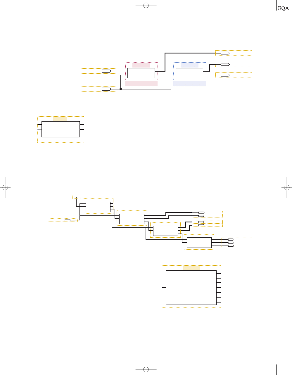
Following the design hierarchy that we established, the next step is
to combine the MOD-6 and MOD-10 counters to make a MOD-60 block.
software uses graphic design files (.gdf) to integrate the
block symbols by drawing lines that connect the input ports, symbols, and
output ports. Quartus II software provides the same feature but uses block
design files (.bdf). The result is shown in Figure 10-32, which represents a
GDF file in
or a BDF file in Quartus II. This graphic or block
design file can be compiled and used to simulate the operation of the MOD-
60 counter. When the design has been verified as working properly, the
or Quartus II system allows us to take this circuit and create
a block symbol for it, as shown in Figure 10-33.
The MOD-60 symbol can be used repeatedly along with the MOD-12 sym-
bol to create the system-level block symbol diagram shown in Figure 10-34.
Even this system-level diagram can be represented by a block symbol for the
entire project, as shown in Figure 10-35.
MAX + PLUS
II
MAX + PLUS
II
MAX + PLUS
II
706
C
HAPTER
10/
D
IGITAL
S
YSTEM
P
ROJECTS
U
SING
HDL
MOD-10 from AHDL
Q[3 . . 0]
FIG10_26
TC
CLK
ENABLE
Q[2 . . 0]
FIG10_24
TC
CLK
ENABLE
CLK
ENA
units[3..0]
tens[2..0]
TC
MOD-6 from VHDL
FIGURE 10-32
Graphically combining HDL blocks to make a MOD-60.
UNITS[3 . . 0]
TENS[2 . . 0]
TC
mod_60
CLK
ENA
FIGURE 10-33
The
MOD-60 counter.
UNITS[3 . . 0]
TENS[2 . . 0]
TC
MOD_60
CLK
ENA
UNITS[3 . . 0]
TENS[2 . . 0]
TC
MOD_60
CLK
ENA
UNITS[3 . . 0]
TENS[2 . . 0]
TC
MOD_60
CLK
ENA
LOW[3 . . 0]
HI
PM
FIG10_29
CLK
ENA
VCC
hr_ones[3..0]
hr_tens
pm
sec_ones[3..0]
sec_tens[2..0]
min_ones[3..0]
min_tens[2..0]
60_pps
FIGURE 10-34
The complete clock project connected using block symbols.
SEC_ONES[3 . . 0]
SEC_TENS[2 . . 0]
MIN_ONES[3 . . 0]
MIN_TENS[2 . . 0]
HR_ONES[3 . . 0]
HR_TENS
PM
FIG10_34
60_PPS
FIGURE 10-35
The entire clock
represented by one symbol.
Combining Blocks Using Only HDL
The graphic approach works well as long as it is available and adequate
for the purpose at hand. As we mentioned previously, HDL was developed
to provide a convenient way to document complex systems and to store the
TOCCMC10_0131725793.QXD 12/19/2005 2:13 PM Page 706
information in a more timeless and software-independent manner. It is reason-
able to assume that with AHDL, the option of graphic integration of subdesigns
will always be available with the tools from Altera; however, this assumption is
not reasonable for users of VHDL. Many VHDL development systems do not
offer any equivalent to the graphic block integration of Altera, which is why
it is important to address the same concept of modular, hierarchical devel-
opment and project integration using only text-based language tools. Our
coverage of AHDL integration will not be as in-depth as our coverage of
VHDL because the graphic method is generally preferred.
S
ECTION
10-4/
D
IGITAL
C
LOCK
P
ROJECT
707
AHDL
FIGURE 10-36
The MOD-60 made from MOD-10 and MOD-6 in AHDL.
INCLUDE “fig10_26.inc”; -- mod-10 counter module
INCLUDE “fig10_23.inc”; -- mod-6 counter module
SUBDESIGN fig10_36
(
clk, ena :INPUT;
ones[3..0], tens[2..0], tc :OUTPUT;
)
VARIABLE
mod10 :fig10_26; -- mod-10 for units
mod6 :fig10_23; -- mod-6 for tens
BEGIN
mod10.clock = clk; -- synchronous clocking
mod6.clock = clk;
mod10.enable = ena;
mod6.enable = mod10.tc; -- cascade
ones[3..0] = mod10.q[3..0]; -- 1s
tens[2..0] = mod6.q[2..0]; -- 10s
tc = mod6.tc; -- Make terminal count at 59
END;
1
2
3
4
5
6
7
8
9
10
11
12
13
14
15
16
17
18
19
20
AHDL MODULE INTEGRATION
Let’s go back to the two AHDL files for the MOD-6 and MOD-10 counters.
How do we combine these files into a MOD-60 counter using only text-based
AHDL? The method is really very similar to that of graphic integration.
Instead of creating a “symbol” representation of the MOD-6 and MOD-10
files, a new kind of file called an “INCLUDE” file is created. It contains all
the important information about the AHDL file it represents. To describe a
MOD-60 counter, a new TDF file, shown in Figure 10-36, is opened. The build-
ing block files are “included” at the top, as shown on lines 1 and 2. Next, the
names that were used for the building blocks are used like library compo-
nents or primitives to define the nature of a variable. On line 10, the variable
mod10 is now used to represent the MOD-10 counter in the other module
(fig10_26).
MOD10 now has all the attributes (inputs, outputs, functional op-
eration) described in fig10_26.tdf. Likewise, on line 11, the variable
mod6 is
given the attributes of the MOD-6 counter of fig10_23.tdf. Lines 13–19 ac-
complish the exact same task as drawing lines on the GDF or BDF file to con-
nect the components to one another and to the input/output ports.
TOCCMC10_0131725793.QXD 12/19/2005 2:13 PM Page 707
This file (FIG10_36.TDF) can be translated into an “include” file (fig10_
36.inc) by the compiler and then used in another tdf file that describes the in-
terconnection of major sections to make up the system. Each level of the hi-
erarchy refers back to the constituent modules of the lower levels.
708
C
HAPTER
10/
D
IGITAL
S
YSTEM
P
ROJECTS
U
SING
HDL
VHDL
FIGURE 10-37
The MOD-60 made from MOD-10 and MOD-6 in VHDL.
ENTITY fig10_37 IS
PORT( clk, ena :IN BIT ;
tens :OUT INTEGER RANGE 0 TO 5;
ones :OUT INTEGER RANGE 0 TO 9;
tc :OUT BIT );
END fig10_37;
ARCHITECTURE a OF fig10_37 IS
SIGNAL cascade_wire :BIT;
COMPONENT fig10_24 -- MOD-6 module
PORT( clock, enable :IN BIT ;
q :OUT INTEGER RANGE 0 TO 5;
tc :OUT BIT);
END COMPONENT;
COMPONENT fig10_27 -- MOD-10 module
PORT( clock, enable :IN BIT ;
q :OUT INTEGER RANGE 0 TO 9;
tc :OUT BIT);
END COMPONENT;
BEGIN
mod10:fig10_27
PORT MAP( clock => clk,
enable => ena,
q => ones,
tc => cascade_wire);
mod6:fig10_24
PORT MAP( clock => clk,
enable => cascade_wire,
q => tens,
tc => tc);
END a;
1
2
3
4
5
6
7
8
9
10
11
12
13
14
15
16
17
18
19
20
21
22
23
24
25
26
27
28
29
30
31
32
33
VHDL MODULE INTEGRATION
Let’s go back to the two VHDL files for the MOD-6 and MOD-10 counters,
which were shown in Figures 10-24 and 10-27, respectively. How do we com-
bine these files into a MOD-60 counter using only text-based VHDL? The
method is really very similar to that of graphic integration. Instead of creat-
ing a “symbol” representation of the MOD-6 and MOD-10 files, these design
files are described as a COMPONENT, like we studied in Chapter 5. It con-
tains all the important information about the VHDL file it represents. To de-
scribe a MOD-60 counter, a new VHDL file, shown in Figure 10-37, is opened.
The building block files are described as “components,” as shown on lines
TOCCMC10_0131725793.QXD 12/19/2005 2:13 PM Page 708
S
ECTION
10-4/
D
IGITAL
C
LOCK
P
ROJECT
709
FIGURE 10-38
The complete clock in VHDL.
ENTITY fig10_38 IS
PORT( pps_60 :IN BIT ;
hour_tens :OUT INTEGER RANGE 0 TO 1;
hour_ones, min_ones, sec_ones :OUT INTEGER RANGE 0 TO 9;
min_tens, sec_tens :OUT INTEGER RANGE 0 to 5;
pm :OUT BIT );
END fig10_38;
ARCHITECTURE a OF fig10_38 IS
SIGNAL cascade_wire1, cascade_wire2, cascade_wire3 :BIT;
SIGNAL enabled :BIT;
COMPONENT fig10_37 -- MOD-60
PORT( clk, ena :IN BIT ;
tens :OUT INTEGER RANGE 0 TO 5;
ones :OUT INTEGER RANGE 0 TO 9;
tc :OUT BIT );
END COMPONENT;
COMPONENT fig10_29 -- MOD-12
PORT( clk, ena :IN BIT ;
low :OUT INTEGER RANGE 0 TO 9;
hi :OUT INTEGER RANGE 0 TO 1;
pm :OUT BIT );
END COMPONENT;
BEGIN
enabled <= ’1’;
prescale:fig10_37 -- MOD-60 prescaler
PORT MAP( clk => pps_60,
ena => enabled,
tc => cascade_wire1);
second:fig10_37 -- MOD-60 seconds counter
PORT MAP( clk => pps_60,
ena => cascade_wire1,
ones => sec_ones,
tens => sec_tens,
tc => cascade_wire2);
minute:fig10_37 -- MOD-60 minutes counter
PORT MAP( clk => pps_60,
ena => cascade_wire2,
ones => min_ones,
tens => min_tens,
tc => cascade_wire3);
hour:fig10_29 -- MOD12 Hours Counter
PORT MAP( clk => pps_60,
ena => cascade_wire3,
low => hour_ones,
hi => hour_tens,
pm => pm);
END a;
1
2
3
4
5
6
7
8
9
10
11
12
13
14
15
16
17
18
19
20
21
22
23
24
25
26
27
28
29
30
31
32
33
34
35
36
37
38
39
40
41
42
43
44
45
46
47
48
49
50
51
52
TOCCMC10_0131725793.QXD 12/19/2005 2:13 PM Page 709
10–14 and lines 15–19 in the architecture description. Next, the names that
were used for the building blocks (components) are used along with the
PORT MAP keywords to describe the interconnection of these components.
The information in the PORT MAP sections describes the exact same opera-
tions as drawing wires on a schematic diagram in a GDF file or BDF file.
Finally, the VHDL file that represents the block at the top of the hierarchy
is created using components from Figure 10-37 (MOD-60) and Figure 10-29
(MOD-12). This file is shown in Figure 10-38. Notice that the general form is
as follows:
Define I/O: lines 1–7
Define signals: lines 10–11
Define components: lines 12–23
Instantiate components and connect them together: lines 27–52
710
C
HAPTER
10/
D
IGITAL
S
YSTEM
P
ROJECTS
U
SING
HDL
REVIEW QUESTIONS
1. What is being defined at the top level of a hierarchical design?
2. Where does the design process start?
3. Where does the building process start?
4. At which stage(s) should simulation testing be done?
10-5
FREQUENCY COUNTER PROJECT
The project in this section demonstrates the use of counters and other stan-
dard logic functions to implement a system called a frequency counter,
which is similar to the piece of test equipment that you have probably used
in the laboratory. The theory of operation will be described in terms of con-
ventional MSI logic devices and then related to the building blocks that can
be developed using HDL. As with most projects, this example consists of sev-
eral circuits that we have studied in earlier chapters. They are combined
here to form a digital system with a unique purpose. First, let us define a fre-
quency counter.
A
frequency counter is a circuit that can measure and display the fre-
quency of a signal. As you know, the frequency of a periodic waveform is
simply the number of cycles per second. Shaping each cycle of the unknown
frequency into a digital pulse allows us to use a digital circuit to count the
cycles. The general idea behind measuring frequency involves enabling a
counter to count the number of cycles (pulses) of the incoming waveform
during a precisely specified period of time called the
sampling interval. The
length of the sampling interval determines the range of frequencies that can
be measured. A longer interval provides improved precision for low frequen-
cies but will overflow the counter at high frequencies. A shorter sample in-
terval provides a less precise measurement of low frequencies but can measure
a much higher maximum frequency without exceeding the upper limit of the
counter.
EXAMPLE 10-1
Assume that a frequency counter uses a four-digit BCD counter. Determine
the maximum frequency that can be measured using each of the following
sample intervals:
(a) 1 second
(b) 0.1 second
(c) 0.01 second
TOCCMC10_0131725793.QXD 12/19/2005 2:13 PM Page 710
Solution
(a) With a sampling interval of 1 second, the four-digit counter can count up
to 9999 pulses. The frequency is 9999 pulses per second or 9.999 kHz.
(b) The counter can count up to 9999 pulses within the sampling interval of
0.1 second. This translates into a frequency of 99,990 pulses per second
or 99.99 kHz.
(c) The counter can count up to 9999 pulses within the sampling interval of
0.01 second. This translates into a frequency of 999,900 pulses per sec-
ond or 999.9 kHz.
S
ECTION
10-5/
F
REQUENCY
C
OUNTER
P
ROJECT
711
EXAMPLE 10-2
If a frequency of 3792 pps is applied to the input of the frequency counter,
what will the counter read under each of the following sample intervals?
(a) 1 second
(b) 0.1 second
(c) 10 ms
Solution
(a) During a sampling interval of 1 second, the counter will count 3792 cy-
cles. The frequency will read 3.792 kpps.
(b) During a sampling interval of 0.1 second, the number of pulses that will
be counted is 379 or 380 cycles, depending on where the sample interval
begins. The frequency will read 03.79 kpps or 03.80 kpps.
(c) During a sampling interval of 0.01 second, the number of pulses that will
be counted is 37 or 38 cycles, depending on where the sample interval
begins. The frequency will read 003.7 kpps or 003.8 kpps.
One of the most straightforward methods for constructing a frequency
counter is shown as a block diagram in Figure 10-39. The major blocks are
the counter, the display register, the decoder/display, and the timing and
control unit. The counter block contains several cascaded BCD counters
that are used to count the number of pulses produced by the unknown sig-
nal applied to the clock input. The counter block has count enable and clear
controls. The time period for counting (sample interval) is controlled by an
enable signal that is produced by the timing and control block. The length
Range
select
Clock
generator
Timing and
control
Decoder and
display
Display
register
Cascaded BCD
counters
Pulse
shaper
System
clock
Unknown signal
(frequency = f
x
)
f
x
converted to
digital impulses
Store
Clear
Enable
FIGURE 10-39
Basic
frequency counter block
diagram.
TOCCMC10_0131725793.QXD 12/19/2005 2:13 PM Page 711
of time for the BCD counters to be enabled can be selected with the range
select input to the timing and control block. This allows the user to select
the desired frequency range to be measured and effectively determines the
location of the decimal point in the digital readout. The pulse width of the
enable signal (sample interval) is critical for taking an accurate frequency
measurement. The counter must be cleared before it is enabled for a new
frequency measurement of the unknown signal. After a new count has been
taken, the counter is disabled, and the most recent frequency measurement
is stored in the display register. The output of the display register is input to
the decoder and display block, where the BCD values are converted into
decimal for the display readout. Using a separate display register allows the
frequency counter to take a new measurement in the background so that
the user does not watch the counter while it is totaling the number of pulses
for a new reading. The display is instead updated periodically with the last
frequency reading.
The accuracy of this frequency counter depends almost entirely on the
accuracy of the system clock frequency, which is used to create the proper
pulse width for the counter enable signal. A crystal-controlled clock genera-
tor is used in Figure 10-39 to produce an accurate system clock for the tim-
ing and control block.
A pulse shaper block is needed to ensure that the unknown signal whose
frequency is to be measured will be compatible with the clock input for the
counter block. A Schmitt-trigger circuit may be used to convert “nonsquare”
waveforms (sine, triangle, etc.) as long as the unknown input signal is of sat-
isfactory amplitude. If the unknown signal might have a larger or smaller
amplitude than is compatible with a given Schmitt trigger, then additional
analog signal conditioning circuitry, such as an automatic gain control, will
be required for the pulse shaper block.
The timing diagram for the control of the frequency counter is shown in
Figure 10-40. The control clock is derived from the system clock signal by
frequency dividers contained in the control and timing block. The period of
the control clock signal is used to create the desired enable pulse width. A
recycling control counter inside the control and timing block is clocked by the
control clock signal. It has selected states decoded to produce the repeating
712
C
HAPTER
10/
D
IGITAL
S
YSTEM
P
ROJECTS
U
SING
HDL
Unknown
signal
Control
clock
Control
counter
Clear
Enable
Store
Digital
pulses
Control
events
state5
state0
state1
state2
state3
state4
state5
Clear counter
Counts pulses during this time interval
Store count in display register
Repeats
FIGURE 10-40
Frequency counter timing diagram.
TOCCMC10_0131725793.QXD 12/19/2005 2:13 PM Page 712
control signal sequence (clear, enable, and store). The counter (cascaded
BCD stages) is first cleared. Then the counter is enabled for the proper
sample interval to count the digital pulses, which have the same frequency
as the unknown signal. After disabling the counter, the new count is stored
in the display register.
The counter, display register, and decoder/display sections are straight-
forward and are not described any further here. The timing and control block
provides the “brains” for our frequency counter and deserves a little more
discussion to explain its operation. Figure 10-41 shows the sub-blocks within
the timing and control block. For our example design, we will assume that
the clock generator produces a 100-kHz system clock signal. The system
clock frequency is divided by a set of five decade counters (MOD-10). This
gives the user six different frequencies that can be selected by the multi-
plexer for the control clock frequency using the range select control.
Because the period of the control clock is the same as the pulse width of the
counter enable, this setup allows the frequency counter to have six different
frequency measurement ranges. The control counter is a MOD-6 counter that
has three selected states decoded by the control signal generator to produce
the clear, enable, and store control signals.
S
ECTION
10-5/
F
REQUENCY
C
OUNTER
P
ROJECT
713
Store
Clear
Decade
counter
DIV10
10 Hz
Decade
counter
DIV10
100 Hz
Decade
counter
DIV10
1 kHz
Decade
counter
DIV10
10 kHz
System clock
100kHz
Decade
counter
DIV10
Control
clock
Range select
MUX
1 Hz
1 s
100 ms
10 ms
1 ms
0.1 ms
0.01 ms
Control
counter
MOD-6
Control signal
generator
(decoder)
Enable
FIGURE 10-41
Timing and control block for frequency counter.
EXAMPLE 10-3
Assume that the BCD counter in Figure 10-39 consists of three cascaded BCD
stages and their associated displays. If the unknown frequency is between 1
kpps and 9.99 kpps, which range (sample interval) should be selected using
the MUX of Figure 10-41?
TOCCMC10_0131725793.QXD 12/19/2005 2:13 PM Page 713
Solution
With three BCD counters, the total capacity of the counter is 999. A 9.99-kpps
frequency produces a count of 999 if a 0.1-s sample interval were used. Thus,
in order to use the full capacity of the counter, the MUX should select the
0.1-s clock period (10 Hz). If a 1-s sampling interval were used, the counter
capacity would always be exceeded for frequencies in the specified range. If
a shorter sample interval were used, the counter would count only between
1 and 99, which would give a reading to only two significant figures and
would be a waste of the counter’s capacity.
714
C
HAPTER
10/
D
IGITAL
S
YSTEM
P
ROJECTS
U
SING
HDL
REVIEW QUESTIONS
1. What is the purpose of running the unknown signal through a pulse
shaper?
2. What are the units of a frequency measurement?
3. What does the display show during the sample interval?
SUMMARY
1. Successful project management can be accomplished by the following
steps: overall project definition; breaking the project into small, strate-
gic pieces; synthesis and testing of each piece; and system integration.
2. Small projects like the stepper motor driver can be completed in a single
design file, even though these projects are developed modularly.
3. Projects that consist of several simple building blocks, like the keypad
encoder, can produce very useful systems.
4. Larger projects like the digital clock can often take advantage of stan-
dard common modules that can be used repeatedly in the overall design.
5. Projects should be built and tested in modules starting at the lowest lev-
els of hierarchy.
6. Preexisting modules can easily be combined with new custom modules
using both graphical and text-based description methods.
7. Modules can be combined and represented as a single block in the next
higher level of the hierarchy using the Altera design tools.
IMPORTANT TERMS
nesting
hierarchy
prescaler
frequency counter
sampling interval
PROBLEMS
SECTION 10-1
10-1. The security monitoring system of Section 9-8 in Chapter 9 can be de-
veloped as a project.
(a) Write a project definition with specifications for this system.
(b) Define three major blocks of this project.
(c) Identify the signals that interconnect the blocks.
B
TOCCMC10_0131725793.QXD 12/19/2005 2:13 PM Page 714

(d)*At what frequency must the oscillator run for a 2.5-Hz flash rate?
(e)*Why is it reasonable to use only one current limiting resistor for
all eight LEDs?
SECTION 10-2
Problems 10-2 through 10-7 refer to stepper motors described in Section 10-2.
10-2.*How many full steps must occur for a complete revolution?
10-3.*How many degrees of rotation result from one compete cycle through
the full-step sequence in Table 10-1?
10-4. How many degrees of rotation result from one complete cycle through
the half-step sequence in Table 10-1?
10-5. The
cout lines of Figure 10-1 started at 1010 and have just progressed
through the following sequence: 1010, 1001, 0101, 0110.
(a)*How many degrees has the shaft rotated?
(b) What sequence will reverse the rotation and return the shaft to its
original position?
10-6. Describe a method to test the stepper driver in:
(a) Full-step mode
(b) Half-step mode
(c) Wave-drive mode
(d) Direct-drive mode
10-7. Rewrite the stepper driver design file of Figure 10-8 or 10-9 without
using a CASE statement. Use your favorite HDL.
10-8. Modify the stepper design file of Figure 10-8 or 10-9 to add an enable
input that puts the outputs in the Hi-Z state (tristate) when enable
SECTION 10-3
10-9. Write the state table for the ring counter shown in Figure 10-11 and
described in Figure 10-13.
10-10.*With no keys pressed, what is the value on c[3..0]?
10-11. Assume that the ring counter is in state 0111 when someone presses
the 7 key. Will the ring counter advance to the NEXT state?
10-12. Assume the 9 key is pressed and held until
(a)*What is the value on the ring counter?
(b) What is the value encoded by the row encoder?
(c) What is the value encoded by the column encoder?
(d) What binary number is on the D[3..0] lines?
10-13.*In Problem 10-12, will the data be valid on the falling edge of DAV?
10-14. If you wanted to latch data from the keypad into a 74174 register,
which signal from the keypad would you connect to the clock of the
register? Draw the circuit.
10-15.*The keypad is connected to a 74373 octal transparent latch as shown
in Figure 10-42. The output is correct as long as a key is held. However,
it is unable to latch data between key presses. Why will this circuit
not
work correctly?
DAV = 1.
=
0.
P
ROBLEMS
715
*Answers to problems marked with an asterisk can be found in the back of the text.
B
B
B
B
B
D, H
D, H
B
B
B
B
B
B, D
T
TOCCMC10_0131725793.QXD 12/19/2005 2:13 PM Page 715
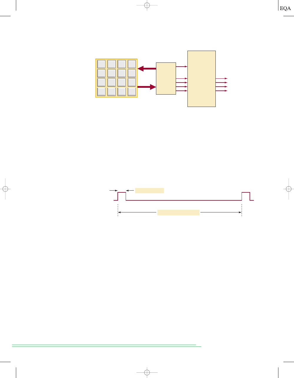
SECTION 10-4
10-16. Assume a 1-Hz clock is applied to the seconds stage of the clock in
Figure 10–17. The MOD-10
units of seconds counter’s terminal count
(
tc) output is shown in Figure 10-43. Draw a similar diagram showing
the number of clock cycles between the
tc output pulses of each of the
following:
(a)*Tens of seconds counter
(b) Units of minutes counter
(c) Tens of minutes counter
716
C
HAPTER
10/
D
IGITAL
S
YSTEM
P
ROJECTS
U
SING
HDL
Terminal count (tc)
1 clock cycle (1 s)
10 clock cycles (T
clk
= 1 s)
FIGURE 10-43
Problem 10-16.
F
B
7
3
E
A
2
D
9
5
1
C
8
4
0
6
Latch
DAV
D
3
D
2
D
1
D
0
Q
3
Q
2
Q
1
Q
0
D
3
D
2
D
1
D
0
En
Outputs
Encoder
Keypad
FIGURE 10-42
Problem 10-15.
10-17.*How many cycles of the 60-Hz power line will occur in a 24-hour pe-
riod? What problem do you think will result if we attempt to simulate
the operation of the entire clock circuit?
10-18.*Many digital clocks are set by simply making them count faster while
a push button is held down. Modify the design to add this feature.
10-19. Modify the hours stage of Figure 10-18 to keep military time (00–23
hours).
SECTION 10-5
10-20. Draw the hierarchy diagram for the frequency counter project.
10-21. Write the HDL code for the MOD-6 control counter and control signal
generator in Figure 10-41.
10-22.*Write the HDL code for the MUX of Figure 10-41.
10-23. Use graphic design techniques and the BCD counter described in Figure
10-31, the MUX, and the control signal generator design to create the
entire timing and control block for the frequency counter project.
10-24. Write the HDL code for the timing and control section of the fre-
quency counter.
B
B
D
D, H
B
D, H
D, H
D
D, H
TOCCMC10_0131725793.QXD 12/19/2005 2:13 PM Page 716
ANSWERS TO SECTION REVIEW QUESTIONS
SECTION 10-1
1. Definition, strategic planning, synthesis and testing, system integration and
testing
2. The definition stage
SECTION 10-2
1. Full-step, half-step, wave-drive, and direct-drive
2.
[mode selector
switches set to (1,1)]
3. Step, direction [mode selector switches set to (0,1)]
4. Eight states
SECTION 10-3
1. Only one
2. The first one scanned after being pressed (usually the first one
pressed)
3. To make DAV go HIGH after the data stabilizes
4. No, it goes
HIGH on the next clock after the key is pressed.
5. Whenever OE is LOW or
when no keys are pressed
SECTION 10-4
1. The overall operating specifications and the system inputs and outputs.
2. At the top of the hierarchy
3. At the bottom, building the simplest blocks first
4. At each stage of modular implementation
SECTION 10-5
1. To change the shape of the analog signal into a digital signal of the same
frequency
2. Cycles per second (Hz) or pulses per second (pps)
3. The
display shows the frequency measured during the previous sample interval.
cin
0
-cin
3
A
NSWERS TO
S
ECTION
R
EVIEW
Q
UESTIONS
717
TOCCMC10_0131725793.QXD 12/19/2005 2:13 PM Page 717
Wyszukiwarka
Podobne podstrony:
Digital Systems Chapter06
Digital Systems Chapter03
Digital Systems Chapter02
Digital Systems Chapter01
Digital Systems Chapter13
digital systems
Digital Systems Cover
Digital Systems Glossary
Digital Systems IndexOfICs
Digital Systems Answers
Digital Systems Index
Digital Systems Theoremspdf
Essentials of Management Information Systems 8e Chapter08
Essentials of Management Information Systems 8e Chapter01
Essentials of Management Information Systems 8e Chapter04
Essentials of Management Information Systems 8e Chapter09
Essentials of Management Information Systems 8e Chapter07
więcej podobnych podstron