AN-948 (v.Int)
Linear Power Amplifier Using Complementary HEXFETs
®
(HEXFET is the trademark for International Rectifier Power MOSFETs)
Topics covered:
A description of the circuit
Performance
Power supply requirements
Set-up and troubleshooting
Performance summary
Related topics
The class AB amplifier described in this application note uses a complementary pair of HEXFET Power MOSFET devices as the
output stage. This feature offers performance improvements over the equivalent bipolar output stage and allows a reduction in the
complexity of the driver circuit, the output devices being driven by a single class A driver. At the time the work was done, logic
level HEXFET Power MOSFETs were not available and standard devices were used. The use of low-threshold devices would
simplify the bias circuit and reduce the quiescent power dissipation The design described will deliver 60W rms into a 4 ohm load
when working from +30V supplies. The bandwidth is in, excess of l00kHz, but may be tailored to the user requirements by
making component value changes.
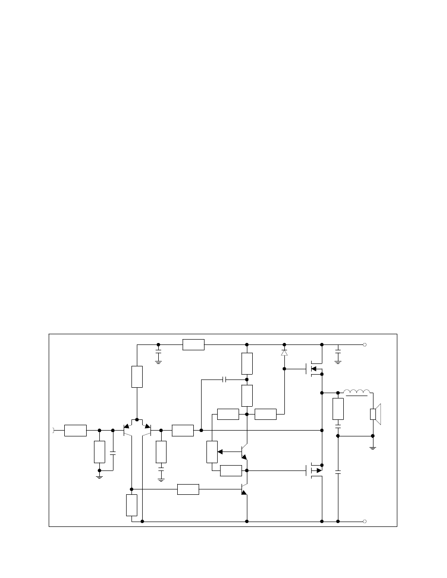
1. CIRCUIT DESCRIPTION
The amplifier circuit diagram is shown in Figure 1, and the components listing in Table 1. Split power supply rails (
±
V
DD
) are
used, giving improved rejection of power supply ripple and allowing the load, R
load
, to be direct coupled. The output devices Q
5
,
Q
6
, operate in source follower configuration. This offers a twofold advantage; a) the possibility of oscillation in the power output
stage is reduced as the voltage gain is less than unity and b) signal feedback through the heatsink on which the devices are
assembled is eliminated as the drain terminal, which is electrically connected to the tab on the TO220 package, is at dc voltage.
Symmetrical output is achieved by providing "bootstrapped" drive to the gate of the n-channel device, Q
5
, from the output. The
use of the bootstrap circuit, C
4
, R
8
, R
9
also allows the driver transistor, Q
4
, to operate at near constant current which improves
the linearity of the driver stage. The diode D
1
acts as a clamp for the bootstrap circuit, restricting the positive voltage at the gate
of Q
5
to +V
DD
. This allows symmetry to be maintained under overload conditions.
Figure 1. Class AB Amplifier Circuit Diagram
R1
R2
C1
R5
Q1
Q2
R7
R6
C2
+
R3
C3
+
R4
R11
R8
R9
R10
C4
+
R12
R13
Q3
R14
Q4
Q5
Q6
D1
C5
+
R15
C7
C6
+
L1
R
LOAD
INPUT
- V
DD
- V
DD
AN-948 (v.Int)
Transistor Q
3
and resistors R
11
, R
12
, R
13
provide gate-source offset voltage for the output devices. R
12
is variable, allowing
adjustment of the output quiescent current for variation in HEXFET Power MOSFET threshold voltage. A degree of temperature
compensation is built into the circuit as both the bipolar transistor, Q
3
, emitter base voltage and the combined threshold voltages
of the HEXFET Power MOSFETs, Q
5
, Q
6
have a temperature coefficient of -0.3%/°C.
Components List
R
1
4.7K
Ω
R
9
2.7K
Ω
C
1
220 pF
Q
1
, Q
2
,
2N4356, 2N5086
R
2
47K
Ω
R
10
680
Ω
C
2
100
µ
F 10V
or equivalent
R
3
15K
Ω
R
11
10K
Ω
C
3
47
µ
F 40V
Q
3
, Q
4
,
2N4410, 2N5088
R
4
1.2K
Ω
R
12
1K
Ω
Pot.
C
4
47
µ
F 40V
or equivalent
R
5
560
Ω
R
13
820
Ω
C
5
2200
µ
F 40V
Q
5
IRF532
R
6
47K
Ω
R
14
4.7K
Ω
C
6
2200
µ
F 40V
Q
6
IRF9532
R
7
4.70
Ω
R
15
10
Ω
1 W
C
7
68 nF
D
1
IN4002
R
8
2.7K
Ω
R
load
8/4
Ω
L
1
3
µΗ
aircored
Table 1. Components List
The class A driver transistor, Q
4
, operates at a bias current determined by resistors R
8
, R
9
, nominally 5mA. Q
4
is driven by a PNP differential
input pair, Q
1
, Q
2
. The bias current in
the input stage is set to 2mA by
resistor R
3
. Negative feedback from
the output of the amplifier is fed to
the base of Q
2
by resistor R
6
. Com-
ponents R
7
, C
2
set the closed loop
gain of the amplifier (R
6
/R
7
) and
provide low frequency gain
boosting. The additional
components R
15
, C
7
connected
between the output node and ground
suppress the high frequency
response of the output stage,
allowing the h.f. performance of the
amplifier to be determined by the
input circuit. Components R
1
, R
2
,
C
1
at the input of the amplifier
define the input impedance
(47Kohm) and suppress noise.
The amplifier input stage requires
additional power supply ripple sup-
pression which is provided by com-
ponents R
4
, C
3
.
Additional circuit components have
been added to ensure high fre-
quency stability of the complete
amplifier. Placement of the compo-
nents and component values will
depend to some extent on the
printed circuit board layout. The
following rules should be followed
when designing the printed circuit
board:
(a) A 'common ground'
principle should be
C5
Q5
R8
R9
C4
R5
R3
R12
C3
R15
C2
C6
Q6
D1
R10
R11
Q3
R13
C7
R6
R14
Q4
R4
Q3
Q2
R7
R2
C1
R1
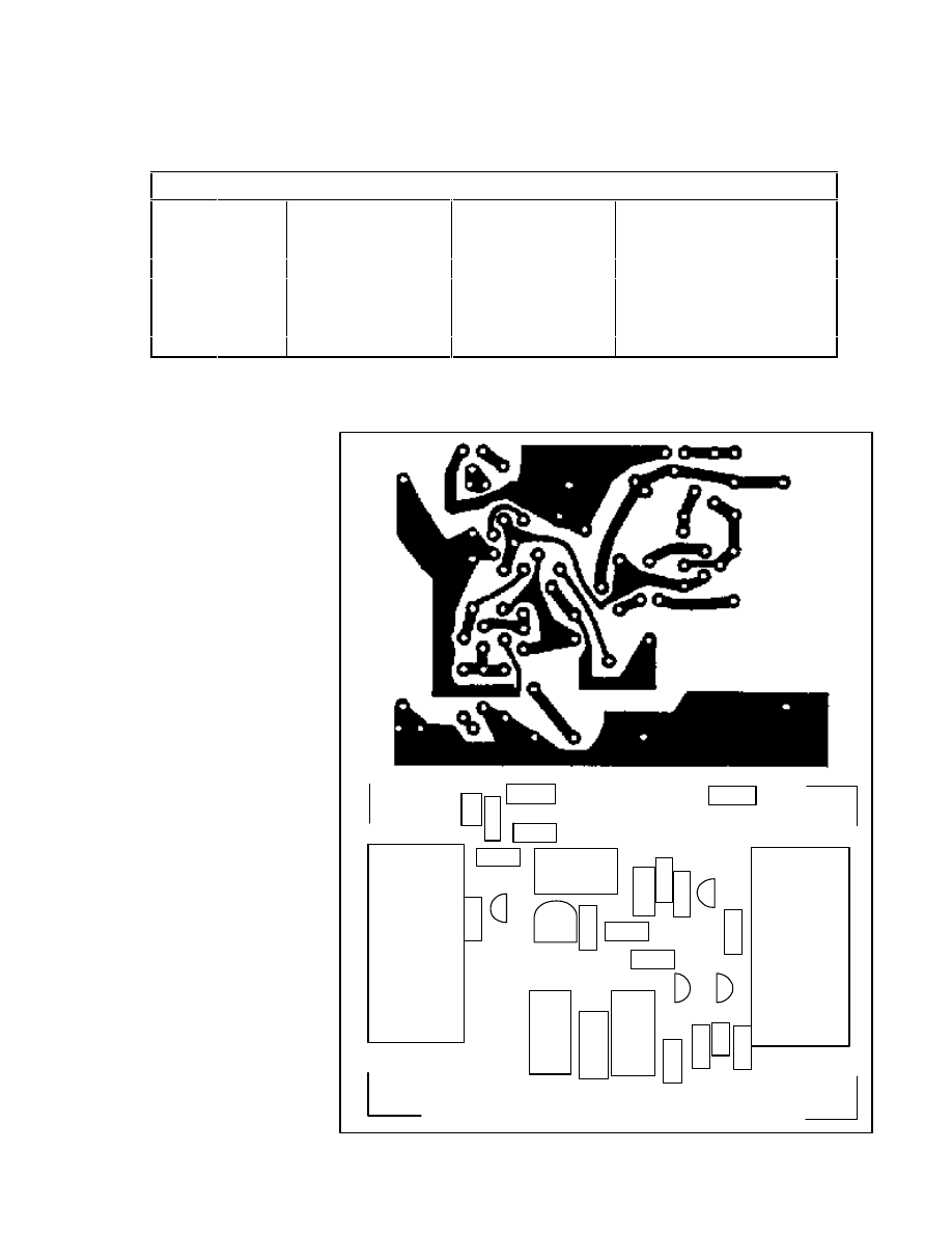
Figure 2. Amplifier Printed Circuit Board Layout
AN-948 (v.Int)
adopted, i.e., power supply decoupling capacitors, load and input stage biasing components should all be taken to
ground in close proximity, eliminating the effects of common node ground current. Similarly, a "common output
node" should be used, the load, feedback resistor and h.f. suppression components being taken from a common
point on the pcb.
(b) The length of connecting lead to the gate terminals of HEXFET Power MOSFETs Q
5
, Q
6
should be an absolute
minimum to avoid oscillation of the power output stage. A series gate resistor, R
10
, may be used to suppress
oscillation, but too high a resistor value will limit the slew rate. Oscillation of the amplifier caused by capacitive
coupling to the base of the driver transistor, Q
4
, is suppressed by the addition of a series resistor, R
14
.
(c) Phase shift in the amplifier when driving a reactive load can lead to high frequency instability. With a capacitive
load, the addition of a small, air-cored choke (3
µ
H with an 8 ohm, 2
µ
F load) will restore stability. The final value
of the choke is defined by experiment.
Figure 2 shows a printed circuit layout which can be used for the circuit shown in Figure 1. The preceding design rules have been
followed.
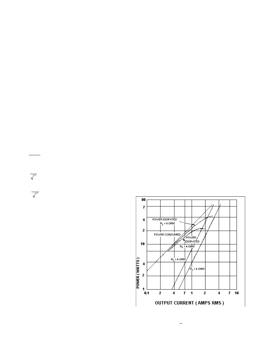
2. AMPLIFIER PERFORMANCE
(a) Output Power: To achieve 60W rms into a 4 ohm load, the current in the load is 3.9A rms or 5.5A pk. This information is
derived from equations (1) and (2):
P
I
R
V
R
O
rms
load
rms
load
=
=
2
2
(1)
I
I
rms
pk
=
2
(2)
V
V
rms
pk
=
2
(3)
Also from equation (1), the voltage developed across the load
at 60W output is 15.5V rms or 22V pk. To sustain a source
current of 5.5A, the n-channel HEXFET Power MOSFET,
IRF530, requires a gate-source voltage of 5V. One can
conclude that the gate bias voltage to achieve peak power in
the positive sense is V
pk
+ V
p
= 27V. A similar calculation
for the negative peak, using the P channel HEXFET Power
MOSFET IRF9530, shows that a negative gate bias supply of
-28V is required.
Consequently, a
±
30V supply will be adequate for a 60W
output, provided that the supply voltage does not fall below
±
28V when loaded, i.e., the power supply impedance should
be better than 1 ohm. The relationship between the power
delivered to the load and the power absorbed from the supply
is shown in Figure 3, assuming a sinusoidal waveform and a
±
30V supply. The curve representing the power delivered to
the load can be easily plotted with the help of equation (1)
for different values of load current.
Figure 3. Power Curves for the Amplifier with 4 and 8 Ohm
Loads and + 30V Power Suuplies
AN-948 (v.Int)
The power absorbed from the supply has been plotted with the help of the following relationship:
( )( )
(
)
P
V
I
V
I
S
avg
avg
DC
rms
=
=
2
2
π
(4)
The difference between the two is the power dissipated in the HEXFET Power MOSFETs and as it can be seen from Figure 3, it
has a peak of approximately 46W. Assuming a maximum ambient temperature of 55°C, the total thermal resistance between the
junction of the two HEXFET Power MOSFETs and the ambient will have to be less than 2°C/W. Considering that the IRF530
and IRF9530 have a thermal resistance between junction and case of 1.7°C/W each, the maximum case temperature will have to
be less than 110°C and the thermal resistance of the heatsink will have to be less than 1.15°C/W to ambient.
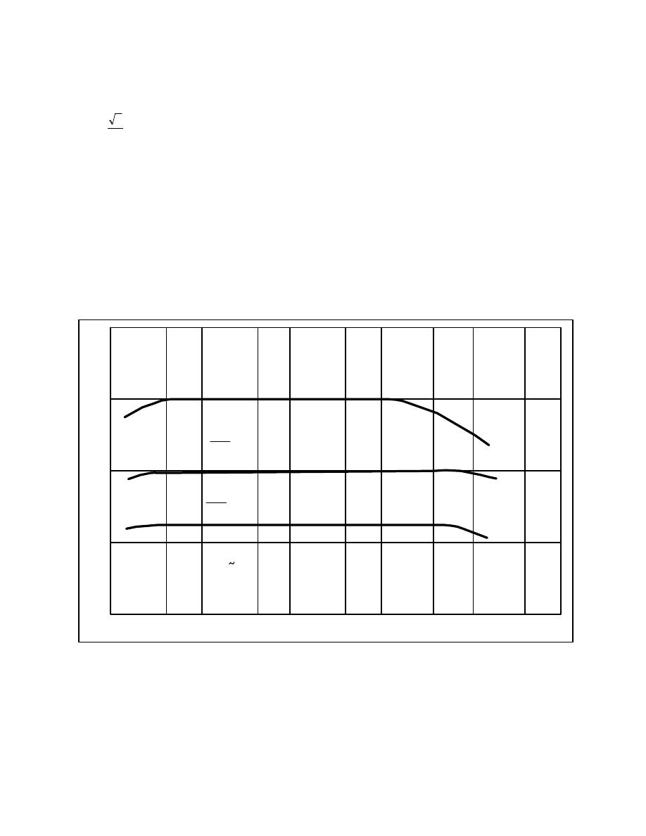
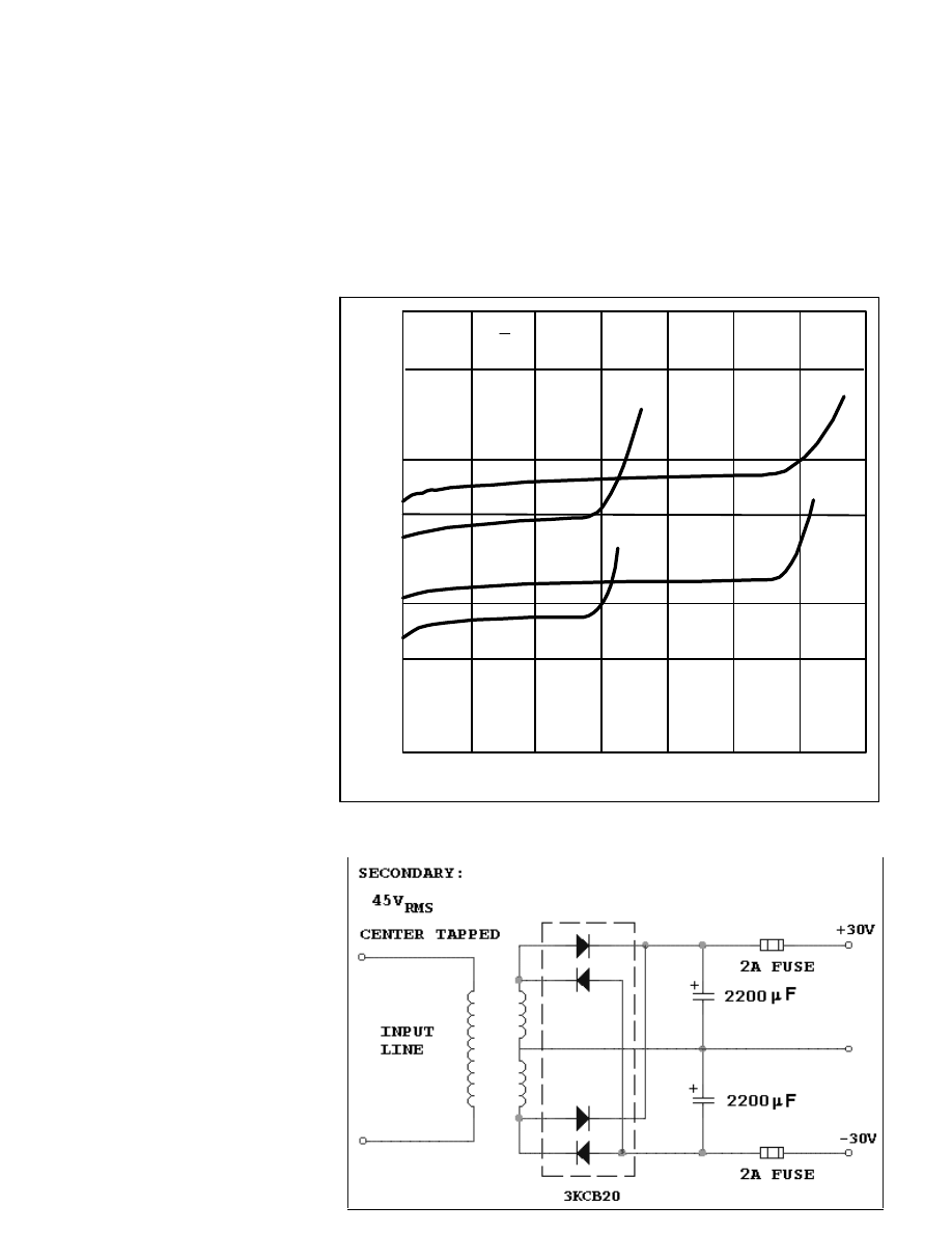
(b) Frequency Response: Open shown in Figure 4. The open loop gain, measured with gate and source connections
to the HEXFET Power MOSFETs broken, is 30db, -3db points occurring at 15 Hz and 60kHz. Closed loop curves are shown for
amplifier gains of 100 (R
7
= 470 ohm) and 20 (R
7
= 2.2K ohm). In both instances the curves remain flat to within +1db between
15 Hz and 100kHz with an 8 ohm load. The slew rate of the amplifier, measured with a 2V pk-pk square wave input is 13V/
µ
s
positive going and 16V/
µ
s negative going. The discrepancy could be balanced out by addition of a series gate resistor for Q
6
.
(c) Total Harmonic Distortion: The fidelity of the amplifier is shown in the distortion curves, Figure 5, and is limited by the loop
gain. Reduction of the closed loop gain from 100 to 20 produces a significant improvement in distortion figure. The output stage
quiescent current was adjusted to 100mA and can influence the distortion measurement significantly if allowed to fall below
50mA.
(d) Quiescent Operating: The dependence of the quiescent current in the output stage and of the offset voltage on power supply
voltage are illustrated in Table 2. The quiescent current is set by first adjusting the potentiometer, R
12
, for minimum offset
voltage-turned fully anticlockwise if the pcb layout in Figure 2 is used - and applying the power supply voltage, the positive
Figure 4. Amplifier Open and Closed Loop Frequency Response Curves
10
1
4
10
2
4
10
3
4
10
4
4
10
5
4
10
6
0
10
20
30
40
FREQUENCY (Hz)
VOLTAGE GAIN (dB)
OPEN
LOOP
R
7
= 100
R
6
R
7
= 100
R
6
V
DD
= = 30V
R
L
= 8OHM
AN-948 (v.Int)
supply passing through an ammeter with 1A f.s.d. R
12
is then adjusted until the meter reading is 100mA with
±
30V supplies.
The meter should be removed from circuit before applying an input signal to the amplifier.
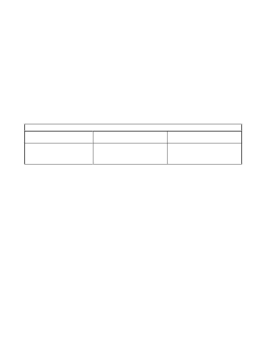
3. POWER SUPPLY REGULATION REQUIREMENTS
A simple line derived power suitable for the class AB amplifier is illustrated in Figure 6. The
±
30V supplies are
taken from the centertapped secondary of the line transformer. The 2200
µ
F decoupling capacitors, (Figure 1) which
should be mounted as close as possible to the amplifier output stage, reduce the supply frequency ripple to 5.5V pk-pk at full
load.
4. SET-UP PROCEDURE AND TROUBLESHOOTING
It is unlikely that any experienced
experimenter will have difficulty in
achieving satisfactory results when
building an amplifier to this design.
The printed circuit board shown in
Figure 2 is intended to assist in this
respect. The major problems antici-
pated are those associated with the
faulty assembly of components and
damage to the HEXFET Power
MOSFETs through handling or
circuit oscillation.
The following troubleshooting
checklist is offered as a guide to the
experimenter:
1. When assembling the printed
circuit board, mount the passive
components first, ensuring the cor-
rect polarity of electrolytic capaci-
tors. Then solder in the transistors
Q
1
- Q
4
checking for correct pin
identification. Finally, mount the
HEXFET Power MOSFETs,
avoiding static discharge by
shorting the pins together to ground
and using a grounded soldering
iron. Check the assembled board for correct component placement. A component side overlay as shown in Figure 2 is useful for
this purpose. Check the copper side of the
board for solder bridges between tracks,
and remove them. Check for dry solder
joints visually and electrically using a
resistance meter and rework, if necessary.
2. Power can now be applied to the
amplifier and the output stage quiescent
current set to between 50 and 100mA.
The potentiometer, R
12
is first adjusted
for minimum offset (fully anticlockwise
on the pcb layout in Figure 2). An
ammeter is connected in series with the
positive supply and selected to read 1A
f.s.d R
12
is adjusted until the ammeter
reads between 50mA and 100mA.
10
1
4
10
0
4
10
-1
4
10
-2
0
10
20
30
40
50
60
GAIN = 20
R
L
= 8 OHM
GAIN = 20
R
L
= 4 OHM
GAIN=100
R
L
= 8 OHM
GAIN = 100 R
L
=4 OHM
V
DD
+ 30V
F
= 1 KHz
OUTPUT POWER (WATTS)
TOTAL HARMONIC DISTORTION %
Figure 5. Amplifier Total Harmonic Distortion Curves
Figure 6. Off-line power supply
AN-948 (v.Int)
Quiescent current setting can be performed without the load connected.
If, however, a loudspeaker load is connected in circuit, it can be protected by a fuse from dc overload. With the quiescent current
set, the output offset voltage can be confirmed to be less than 100mV. Excessive and erratic variation in quiescent current as R
12
is adjusted are indicative of circuit oscillation or faulty wiring. The solutions described in "Circuit Description" (series gate res-
istors, minimized gate wiring and common earthing) should be adopted. Also, supply decoupling capacitors should be mounted
in close proximity to the amplifier output stage and load ground point. Quiescent current setting should be performed with the
HEXFET Power MOSFETs mounted on their heatsink to avoid overdissipation.
3. With the quiescent current set, the ammeter should be removed from the positive supply and a signal can be applied to the
amplifier input. Signal requirements for full rated output are:
gain = 100:
R
L
= 4
Ω
, V
in
= 150mV rms
R
L
= 8
Ω
, V
in
= 160mV rms
gain = 20:
R
L
= 4
Ω
, V
in
= 770mV rms
R
L
= 8
Ω
, V
in
= 800mV rms
Variation in Output Offset Voltage and Output Quiescent Current with Supply Voltage
Supply Voltage
+ V
DD
V
Output Offset
V
OS
mV
Output Quiescent Current
Iq mA
35
30
25
20
-40
-20
+4
+30
135
100
75
54
Table 2. Variation in Output offset voltage and Output quiescent current with supply voltage
"Clipping" of the output waveform when operating at rated power indicates poor supply regulation and can be remedied by
reducing the input signal amplitude and derating the amplifier. Alternatively, a lower impedance supply should be used. The
frequency response of the amplifier can be checked over the frequency range 15 Hz - 100kHz with the aid of an audio test set or
signal generator and oscilloscope. Distortion of the output waveform at high frequency is indicative of a reactive load and
adjustment of the output choke will be required to restore the waveform. The high frequency response may be tailored with a
compensation capacitor in parallel with R
6
. The low frequency response is controlled by components R
7
, C
2
.
4. Hum pickup will be more likely to occur in a high gain circuit. Pickup at the high impedance input is minimized by use of a
shielded cable, grounded at the signal source. Supply frequency ripple injected through the supply to the input stage of the
amplifier can be detected across capacitor, C
3
. This is attenuated by the common mode rejection ratio of Q
1
, Q
2
before being
amplified. However, if this is the source of hum, adjustment to the values of C
3
, R
5
can be made to suppress the signal amplitude.
5. In the event of the output stage being destroyed, either through short circuit load or h.f. oscillation, both HEXFET Power
MOSFETs should be replaced. It is unlikely, however, that other circuit components will have been affected. The setup procedure
should, of course, be repeated with the new devices in circuit.
5. PERFORMANCE SUMMARY
Using a complementary pair of HEXFET Power MOSFETs, IRF530 and IRF9530 and with a
±
30V supply, the following
performance can be achieved:
Maximum rms output power:
60W into 4
Ω
32W into 8
Ω
AN-948 (v.Int)
Bandwidth:
15 Hz to 100kHz
±
1db
Total harmonic distortion (1kHz):
0.15% at 60W into 4
Ω
0.08% at 32W into 8
Ω
Voltage gain:
Adjustable, X100 to X20
Input impedance: 47K
Ω
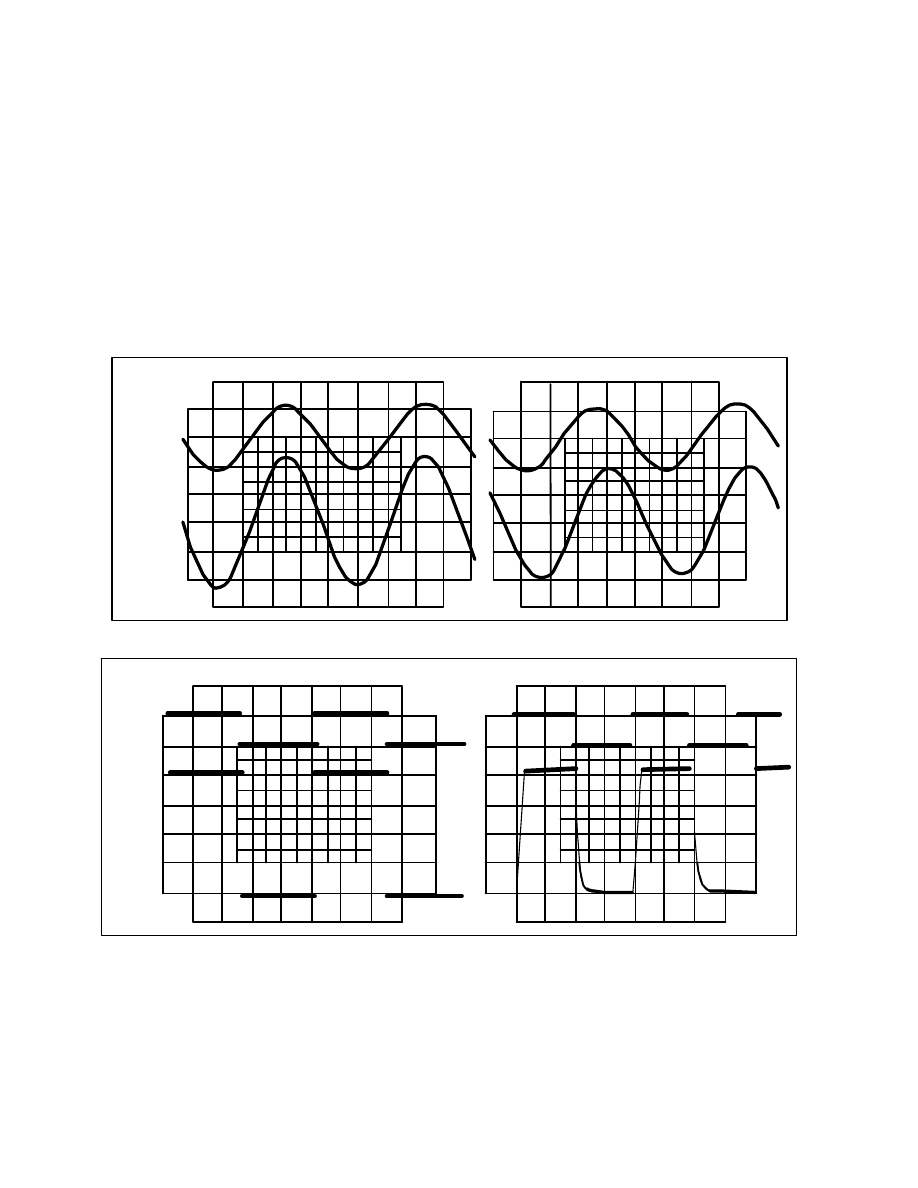
Figure 7a & 7b: Amplifier Waveforms illustrating Frequency Response
Figure 7 illustrates the amplifier response to 1kHz and 100kHz sinewave input signals and also the square wave response at 1kHz
and 25kHz.
Related topics:
P-Channel HEXFET Power MOSFETs
Gate drive requirements
Figure 7a: Sinewave Frequency Response
200
µ
µ
S
1 V
10V
INPUT
OUTPUT
1 KHz
100 KHz
1 V
2
µ
µ
S
10V
10V
2V
10
µ
µ
S
25 KHz
200
µ
µ
S
2V
10V
1 KHz
INPUT
OUTPUT
Figure 7b: Square Wave Response

AN-948 (v.Int)
Thermal design
WORLD HEADQUARTERS: 233 Kansas St., El Segundo California 90245, Tel: (310) 322 3331
EUROPEAN HEADQUARTERS: Hurst Green, Oxted, Surrey RH8 9BB, UK Tel: ++ 44 1883 732020
IR CANADA: 7321 Victoria Park Ave., Suite 201, Markham, Ontario L3R 2Z8, Tel: (905) 475 1897
IR GERMANY: Saalburgstrasse 157, 61350 Bad Homburg Tel: ++ 49 6172 96590
IR ITALY: Via Liguria 49, 10071 Borgaro, Torino Tel: ++39 11 451 0111

AN-948 (v.Int)
IR FAR EAST: K&H Bldg., 2F, 3-30-4 Nishi-Ikeburo 3-Chrome, Toshima-Ki, Tokyo Japan 171 Tel: 81 3 3983
0086
IR SOUTHEAST ASIA: 315 Outram Road, #10-02 Tan Boon Liat Building, Singapore 0316 Tel: 65 221 8371
Data and specification subject to change without notice.
Wyszukiwarka
Podobne podstrony:
BP4078 Class D Audio Power Amplifier
Power 400 Watts Hi Fi High End Audio Power Amplifier
Designing Audio Power Amplifiers
Guidelines For Measuring Audio Power Amplifier Performance (Texas Instruments)
Audio Power Amplifiers ICs 1996
Daniel H Cheever A New Methodology for Audio Frequency Power Amplifier Testing Based On Psychoacoust
McMartin LT2000D Power Amplifier
AGH Analog electronics Chapter III 5 Power amplifiers
Pioneer DEHP825 Power Amplifier Section
20 Watt Channel Stereo Power Amplifier
60 100W Hi Fi Power Amplifier
500W Subwoofer Power Amplifier (Updated)
Power Amplifiers With Valves An Approach And A Practical Circuit (Claus Byrith)
Directory of integrated power amplifiers TDA
JBL Power Amplifier GTS50A
60 Watt Into 8 Ohms Power Amplifier
McMartin LT2000D Power Amplifier
McMartin LT2000D Power Amplifier
Subwoofer Power Amplifier
więcej podobnych podstron